JP5460442B2 - Power supply control device and image forming apparatus - Google Patents
Power supply control device and image forming apparatus Download PDFInfo
- Publication number
- JP5460442B2 JP5460442B2 JP2010098801A JP2010098801A JP5460442B2 JP 5460442 B2 JP5460442 B2 JP 5460442B2 JP 2010098801 A JP2010098801 A JP 2010098801A JP 2010098801 A JP2010098801 A JP 2010098801A JP 5460442 B2 JP5460442 B2 JP 5460442B2
- Authority
- JP
- Japan
- Prior art keywords
- switch
- power supply
- power
- image forming
- forming apparatus
- Prior art date
- Legal status (The legal status is an assumption and is not a legal conclusion. Google has not performed a legal analysis and makes no representation as to the accuracy of the status listed.)
- Expired - Fee Related
Links
Images


Landscapes
- Accessory Devices And Overall Control Thereof (AREA)
- Electrophotography Configuration And Component (AREA)
- Control Or Security For Electrophotography (AREA)
- Facsimiles In General (AREA)
Description
本発明は、電源スイッチの操作に応じて、機器への電源供給を制御する電源供給制御装置、及び画像形成装置に関する。 The present invention relates to a power supply control device that controls power supply to a device in accordance with an operation of a power switch, and an image forming apparatus.
画像形成装置において、電源スイッチがオフ操作された場合に、画像形成装置への給電を即座に遮断してしまうと不都合な場合がある。 In the image forming apparatus, when the power switch is turned off, it may be inconvenient if the power supply to the image forming apparatus is immediately cut off.
例えば、画像データ等を格納するハードディスクを備えた画像形成装置において、ハードディスクへのアクセス中に電源スイッチがオフ操作され、即座に給電が遮断されてしまうと、格納されていたデータが破壊され、その後読み出せなくなる虞がある。 For example, in an image forming apparatus equipped with a hard disk for storing image data or the like, if the power switch is turned off while the hard disk is being accessed and power supply is interrupted immediately, the stored data is destroyed, and then There is a possibility that it cannot be read.
そのため、例えば、特許文献1では、電源スイッチがオフ操作されても、画像形成装置への給電を即座に遮断せずに、所定時間だけ給電を保持する回路を備えた画像形成装置が提案されている。この画像形成装置では、商用電源から画像形成装置への給電ラインを接続するための電源スイッチがオフ操作された場合でも、この電源スイッチと並列に接続されたリレーによって画像形成装置への給電が保持されるように、回路が構成されている。
Therefore, for example,
また、電源スイッチとは別に、電源スイッチに連動して、電源スイッチのオン/オフ状態を検知するスイッチが備えられ、その検知用スイッチは画像形成装置の制御部に接続されている。制御部は検知用スイッチがオフされたことを検知した場合には、画像形成装置で実行中の処理を中止して、電源供給を遮断できる状態へ遷移させる。そして、電源供給を遮断できる状態となった後に、給電を保持していたリレーをオフして、画像形成装置への電源供給を遮断する。 In addition to the power switch, a switch for detecting the on / off state of the power switch is provided in conjunction with the power switch, and the detection switch is connected to the control unit of the image forming apparatus. When the control unit detects that the detection switch is turned off, the control unit stops the process being executed in the image forming apparatus and makes a transition to a state where the power supply can be shut off. Then, after the power supply can be cut off, the relay holding the power supply is turned off to cut off the power supply to the image forming apparatus.
このようにして、特許文献1の画像形成装置においては、電源スイッチがオフ操作されても、画像形成装置への給電を即座に遮断せずに、所定時間だけ給電を保持することを実現させている。
As described above, the image forming apparatus disclosed in
ところで、画像形成装置の電源部への給電経路を接続する電源スイッチには、画像形成装置を動作させるための大電流を流しても耐えられる接点、例えば、銀、又は銀合金を使用した大電流用接点を使用することが要求される。 By the way, the power switch that connects the power supply path to the power supply unit of the image forming apparatus has a contact point that can withstand a large current for operating the image forming apparatus, for example, a large current using silver or a silver alloy. It is required to use a contact for the service.
その一方、電源スイッチのオン/オフ状態を検知する検知用スイッチは給電経路ではないため、大電流を流す必要はない。従って、検知用スイッチに流れる電流は微小な電流に抑え、画像形成装置における消費電力を削減することが望ましい。この検知用スイッチには、微小電流に対応した接点、例えばAu(金)めっき等を施した微小電流用接点を使用することが要求される。 On the other hand, since the detection switch for detecting the on / off state of the power switch is not a power supply path, it is not necessary to flow a large current. Therefore, it is desirable to suppress the current flowing through the detection switch to a very small current and reduce the power consumption in the image forming apparatus. The detection switch is required to use a contact corresponding to a minute current, for example, a contact for minute current subjected to Au (gold) plating.
そのため、大電流用接点を備えた電源スイッチと、微小電流用接点を備えた検知用スイッチの両方を必要とする画像形成装置においては、次のような課題を有していた。 For this reason, an image forming apparatus that requires both a power switch having a large current contact and a detection switch having a minute current contact has the following problems.
例えば、電源スイッチと検知用スイッチが同一のパッケージに実装された専用電源スイッチを用いた場合には、汎用の大電流専用の電源スイッチや、微小電流専用の検知用スイッチに比べ高価であるため、画像形成装置のコストアップを招いてしまう。 For example, when a dedicated power switch in which the power switch and the detection switch are mounted in the same package is used, it is more expensive than a general-purpose large-current dedicated power switch or a micro-current dedicated detection switch. The cost of the image forming apparatus is increased.
また、電源スイッチと検知用スイッチを画像形成装置内に個別に配置し、これら2つのスイッチが同期して動作するように機械的なリンク機構を設けた場合には、リンク機構自体によるコストアップや、リンク機構の配置により装置の小型化が妨げられる。 In addition, when the power switch and the detection switch are individually arranged in the image forming apparatus and a mechanical link mechanism is provided so that these two switches operate in synchronization, the cost increases due to the link mechanism itself. The arrangement of the link mechanism prevents the device from being downsized.
本発明はこのような状況に鑑み、大電流用接点を備えた電源スイッチを用いて、画像形成装置の電源への給電及び給電遮断を行うとともに、電源スイッチのオン/オフ操作を微小電流にて検知することを目的とする。 In view of such a situation, the present invention uses a power switch having a contact point for large current to supply power to the power source of the image forming apparatus and shut off the power supply, and to turn on / off the power switch with a small current. an object of the present invention and the detection child.
前記課題を解決するため、本発明では、次のとおりに構成する。 To solve the above problems, the present invention is configured as follows.
(1)商用電源から電源装置までの給電経路を接続するオン状態と、前記商用電源から前記電源装置までの給電経路を遮断するオフ状態とに切り替わる電源スイッチと、前記電源スイッチと並列に設けられ、短絡又は開放状態に制御されるリレーと、前記電源スイッチのオン/オフ状態を検知する検知回路と、前記検知回路で生成された検知信号に基づいて、前記リレーを短絡又は開放状態に制御する制御手段と、を備え、前記電源スイッチは、第1のスイッチ及び前記第1のスイッチに連動する第2のスイッチを有し、前記第1のスイッチと前記第2のスイッチとが直列に接続され、前記第1のスイッチの他端は前記商用電源に接続され、前記第2のスイッチの他端は前記電源装置に接続され、前記第1のスイッチと前記第2のスイッチとの接続点が、前記検知回路に接続されていることを特徴とする電源供給制御装置。
(2)転写材に画像形成する手段を有する画像形成装置であって、前記画像形成装置の電源供給を制御する手段として、前記(1)項に記載の電源供給制御装置を備えたことを特徴とする画像形成装置。
(1) A power switch that switches between an on state in which a power supply path from a commercial power source to a power supply device is connected and an off state in which the power supply path from the commercial power source to the power supply device is cut off, and the power switch are provided in parallel. The relay is controlled to be short-circuited or opened based on a detection circuit that detects the ON / OFF state of the power switch, and a detection signal generated by the detection circuit. Control means, and the power switch includes a first switch and a second switch that is linked to the first switch, and the first switch and the second switch are connected in series. The other end of the first switch is connected to the commercial power supply, the other end of the second switch is connected to the power supply device, and the first switch and the second switch Connection point, the power supply control apparatus characterized by being connected to the detection circuit.
(2) An image forming apparatus having means for forming an image on a transfer material, wherein the power supply control device according to (1) is provided as means for controlling power supply of the image forming apparatus. An image forming apparatus.
本発明によれば、電源供給制御装置は、廉価な大電流用の電源スイッチを用いて、画像形成装置の電源への給電及び給電遮断を行うとともに、電源スイッチがオン/オフ操作されたことを微小電流にて検知することが可能となる。その結果、画像形成装置の消費電力の低減と、電源スイッチのコスト低減とを図ることができる。 According to the present invention, the power supply control device uses an inexpensive high-current power switch to supply power to the power supply of the image forming apparatus and shut off the power supply, and that the power switch is turned on / off. It is possible to detect with a minute current. As a result, it is possible to reduce the power consumption of the image forming apparatus and the cost of the power switch.
以下、本発明を実施するための形態を、実施形態例により詳しく説明する。 DESCRIPTION OF EMBODIMENTS Hereinafter, embodiments for carrying out the present invention will be described in detail with reference to embodiments.
[第1の実施形態]
以下、本発明に関わる画像形成装置を図面に則して詳しく説明する。
[First Embodiment]
Hereinafter, an image forming apparatus according to the present invention will be described in detail with reference to the drawings.
図1は、本実施形態例の画像形成装置の全体構成を示す概略断面図である。本実施形態例の画像形成装置は、複数の画像形成部を並列に配し、且つ中間転写方式を採用した電子写真カラー複写機である。 FIG. 1 is a schematic cross-sectional view illustrating the overall configuration of the image forming apparatus according to the present exemplary embodiment. The image forming apparatus according to this embodiment is an electrophotographic color copying machine in which a plurality of image forming units are arranged in parallel and an intermediate transfer method is adopted.
図1において、本画像形成装置は、画像読取部1Rと、画像出力部1Pとを有する。画像読取部1Rは、原稿画像を光学的に読み取り、電気信号に変換して画像出力部1Pに送信する。画像出力部1Pは、4つの並設された画像形成部10(10a〜10d)、給紙ユニット20、中間転写ユニット30、定着ユニット40、クリーニングユニット50、70、フォトセンサ60、制御ユニット80を有する。
In FIG. 1, the image forming apparatus includes an
以下では、個々のユニットについて詳しく説明する。 Hereinafter, each unit will be described in detail.
各画像形成部10(10a〜10d)は、イエロー、シアン、マゼンタ、ブラックの色毎に分けられているが、その内部は同一構成となっている。各画像形成部10では、第1の像担持体であるドラム状の電子写真感光体の感光体ドラム11が回転自在に軸支され、矢印方向に回転駆動される。各画像形成部10では、感光体ドラム11の外周面に対向して、その回転方向に1次帯電器12、光学系13、折り返しミラー16、現像装置14、及びクリーニング装置15が配置されている。
Each image forming unit 10 (10a to 10d) is divided into yellow, cyan, magenta, and black colors, and the inside thereof has the same configuration. In each
1次帯電器12は、感光体ドラム11の表面に均一な帯電量の電荷を与える。そして、光学系13により、画像読取部1Rからの記録画像信号に応じて変調した光線(例えばレーザビーム)を、折り返しミラー16を介して感光体ドラム11上に露光することによって、感光体ドラム11上に静電潜像が形成される。
The primary charger 12 applies a uniform charge amount to the surface of the photosensitive drum 11. Then, the light beam (for example, a laser beam) modulated by the optical system 13 in accordance with the recording image signal from the
次に、イエロー、シアン、マゼンタ、ブラックといった4色の現像剤(以下、「トナー」と記す)をそれぞれ収納した現像装置14(14a〜14d)によって、上記静電潜像が顕像化される。顕像化された可視画像は、画像転写領域Ta〜Tdにて、矢印B方向に回転し、第2の像担持体であるベルト状の中間転写体の中間転写ベルト31に転写される。
Next, the electrostatic latent image is visualized by the developing devices 14 (14a to 14d) each containing developer of four colors such as yellow, cyan, magenta, and black (hereinafter referred to as “toner”). . The visualized visible image rotates in the direction of arrow B in the image transfer areas Ta to Td, and is transferred to the
画像転写領域Ta〜Tdの下流側では、クリーニング装置15が、中間転写ベルト31に転写されずに感光体ドラム11上に残されたトナーを掻き落として、ドラム表面の清掃を行う。以上説明したプロセスによって、各トナーによる画像形成が順次行われる。
On the downstream side of the image transfer areas Ta to Td, the cleaning device 15 cleans the drum surface by scraping off the toner that is not transferred to the
給紙ユニット20は、転写材Pを収納するためのカセット21、カセット21より転写材Pを1枚ずつ送り出すためのピックアップローラ22、ピックアップローラ22から送り出された転写材Pをさらに搬送するための給紙ローラ対23、給紙ガイド24を有する。そして、レジストローラ25は、各画像形成部の画像形成タイミングに合わせて、転写材Pを2次転写領域Teへ送り出す。
The
次に、中間転写ユニット30について説明する。
Next, the
中間転写ベルト31は、パルスモータ(不図示)によって回転駆動され、中間転写ベルト31に駆動を伝達する駆動ローラ32と、中間転写ベルト31の回動に従動する従動ローラ33と、2次転写対向ローラ34との間に張設巻回されている。これにより、駆動ローラ32と従動ローラ33の間に、1次転写平面Aが形成される。また、従動ローラ33は、ばね(不図示)の付勢によって中間転写ベルト31に適度なテンションを与えるテンションローラとしての機能も有している。
The
各感光体ドラム11と中間転写ベルト31が対向する1次転写領域Ta〜Tdには、中間転写ベルト31の裏側に1次転写用帯電器35が配置されている。2次転写対向ローラ34に対向して、2次転写ローラ36が配置され、中間転写ベルト31とのニップによって2次転写領域Teが形成される。そして、2次転写ローラ36は、中間転写ベルト31に対して適度な圧力で加圧されている。
A primary transfer charger 35 is disposed on the back side of the
また、中間転写ベルト31の2次転写領域Teの下流には、中間転写ベルト31の画像形成面をクリーニングするためのクリーニングユニット50が配置されている。クリーニングユニット50は、中間転写ベルト31上のトナーを除去するためのクリーニングブレード51と、廃トナーを収納する廃トナーボックス52とを備えている。中間転写ベルト31の裏側には、クリーニングブレード70とクリーニングブレード70を中間転写ベルト31から着脱するためのパルスモータ(不図示)が備えられている。このクリーニングブレード70も、中間転写ベルト31上のトナーを除去するためのものである。
A cleaning unit 50 for cleaning the image forming surface of the
定着ユニット40は、不図示のIHコイルなどの加熱手段を備えた定着ベルト41aと、定着ベルト41aを加圧する加圧ベルト41b(このベルトにも熱源を備える場合もある)とを有する。定着ベルト41aと加圧ベルト41bは、不図示の圧解除ユニットにより離間させることが可能である。
The fixing unit 40 includes a fixing
さらに、定着ユニット40は、定着ベルト41aと加圧ベルト41bとのニップ部へ転写材Pを導くための搬送ガイド43、定着ユニットの熱を内部に閉じ込めるための定着断熱カバー46、47を備えている。
Further, the fixing unit 40 includes a
そして、ニップ部から排出されてきた転写材Pは、内排紙ローラ44、外排紙ローラ45によって装置外部に導き出され、排紙トレイ48上に積載される。
The transfer material P discharged from the nip portion is led out of the apparatus by the inner discharge roller 44 and the
次に、上記構成の画像形成装置の動作について説明する。 Next, the operation of the image forming apparatus having the above configuration will be described.
後述するCPU101aから画像形成動作開始信号が発せられると、画像形成装置は給紙段から給紙動作を開始する。
When an image forming operation start signal is issued from a
図1にて、まず、ピックアップローラ22により、カセット21から転写材Pが1枚ずつ送り出される。そして、給紙ローラ対23によって、転写材Pは給紙ガイド24の間を案内されてレジストローラ25まで搬送される。その時、レジストローラ25は停止しており、転写材Pの先端はニップ部に突き当たる。その後、画像形成部が画像の形成を開始するタイミングに合わせてレジストローラ25は回転を始める。この回転時期は、転写材Pの先端部と、画像形成部より中間転写ベルト31上に転写されたトナー画像の先端部とが、2次転写領域Teにおいて一致するようにそのタイミングが設定されている。
In FIG. 1, first, the transfer material P is sent out one by one from the
また、画像形成動作開始信号が発せられると、中間転写ベルト31の最上流にある画像形成部10dでは、感光体ドラム11d上に形成されたトナー画像が、1次転写用帯電器35dにより、1次転写領域Tdにおいて中間転写ベルト31に転写される。転写されたトナー像は、次の1次転写領域Tcまで搬送される。そこでは、各画像形成部間をトナー像が搬送される時間だけ遅延して画像形成が行われており、前画像の上にレジストを合わせて、その次のトナー像が転写される。以下、同様の工程が繰り返され、その結果、4色のトナー像が中間転写ベルト31上に転写される。
When the image forming operation start signal is issued, the toner image formed on the
そして、転写材Pが2次転写領域Teに送り出され、中間転写ベルト31に接触すると、転写材Pの通過タイミングに合わせて、2次転写ローラ36に高電圧が印加され、中間転写ベルト31上に形成された4色のトナー画像が転写材Pの表面に転写される。その後、転写材Pは搬送ガイド43によって定着ベルトのニップ部まで正確に送り出される。そして、定着ベルト41a、加圧ベルト41bの熱、及びニップ部の圧力によってトナー画像が転写材Pの表面に定着される。その後、内排紙ローラ44、外排紙ローラ45により搬送され、転写材Pは機外に排出され、排紙トレイ48に積載される。
When the transfer material P is sent to the secondary transfer region Te and comes into contact with the
次に、画像形成装置の制御系について説明する。 Next, a control system of the image forming apparatus will be described.
図2は、本実施形態例の画像形成装置の制御系のブロック図を示す。本画像形成装置は、システムコントローラ101によって統括的にコントロールされている。システムコントローラ101は、主に画像形成装置装置内の各負荷の駆動、センサ類の情報収集解析、そして、ユーザインターフェースである操作部102とのデータの交換の役割を担っている。システムコントローラ101には、CPU101aが実装されている。CPU101aは、システムコントローラ101内に実装されたROM101b内に格納されたプログラムに基づいて、予め決められた画像形成シーケンスに関する様々な処理を実行する。また、システムコントローラ101には、CPU101aが処理を行う際に、一次的、又は恒久的にデータを保存するためのRAM101cも実装されている。RAM101cには、例えば、高圧制御部105への高圧設定値や各種データ、操作部102からの画像形成指令情報などが保存される。
FIG. 2 is a block diagram of a control system of the image forming apparatus according to this embodiment. The image forming apparatus is comprehensively controlled by the
操作部102は、ユーザによって入力された複写倍率、濃度設定値などの情報を取得することに加えて、ユーザに対して、画像形成装置の状態、例えば画像形成枚数や画像形成中か否かの情報、ジャムの発生やその箇所等を表示することにも用いられる。
In addition to acquiring information such as a copy magnification and a density setting value input by the user, the
画像形成装置内部の各所には、モータ、クラッチ/ソレノイド等のDC負荷や、フォトインターラプターやマイクロ電源スイッチ等のセンサが配置されている。すなわち、モータの駆動や各DC負荷を適宜駆動させることにより、転写材の搬送や各ユニットの駆動を行っており、その動作を監視しているのが各種センサである。そこで、システムコントローラ101は、各種センサ類109からの信号を基に、モータ制御部107に各モータをコントロールさせると同時に、DC負荷制御部108にクラッチ/ソレノイドを動作させて画像形成動作を円滑に進ませる。また、システムコントローラ101は、高圧制御部105に各種高圧制御信号を送出することにより、高圧ユニット106を構成する各種帯電器に適切な高圧が印加される。
At various locations inside the image forming apparatus, DC loads such as a motor and a clutch / solenoid, and sensors such as a photo interrupter and a micro power switch are arranged. In other words, the transfer material is conveyed and each unit is driven by appropriately driving the motor and each DC load, and various sensors monitor the operation. Therefore, the
定着ユニット40には、定着ベルト41aを加熱するための定着ヒータ111が内蔵されており、そのヒータはACドライバ110によってオン/オフ制御されている。また、定着ベルト41aにはその温度を測定するためのサーミスタ104が設けられている。定着ベルト41aの温度変化に対応したサーミスタ104の抵抗値変化を、A/D103によって電圧値に変換した後、定着ベルト41aの温度データの換算値を示すデジタル値として、システムコントローラ101に入力される。この温度データを基に、システムコントローラ101は、前述のACドライバ110を制御して、定着ヒータ111の温度調整を行う。
The fixing unit 40 incorporates a fixing
また、システムコントローラ101には、ハードディスク112が接続されている。システムコントローラ101は、このハードディスク112に、画像読取部1Rから送信された画像データの保存をしたり、操作部102からのユーザ指示により、ハードディスク112に保存されたデータを読み出して印刷等を行う。
A
続いて、図3を用いて、画像形成装置の電源部について説明する。 Next, the power supply unit of the image forming apparatus will be described with reference to FIG.
図3は、本実施形態例における画像形成装置の電源部のブロック図である。図3において、201は画像形成装置に実装された電源である。電源201に商用電源が入力されると、電圧12Vが生成され、この電圧12Vがシステムコントローラ101に供給されて、システムコントローラが起動される。
FIG. 3 is a block diagram of the power supply unit of the image forming apparatus according to the present exemplary embodiment. In FIG. 3,
システムコントローラ101は起動されると、電源201へリモート信号Sig1を出力する。電源201はこのリモート信号Sig1が入力されると電圧24Vを出力する。この電圧24Vは、システムコントローラ101の他、図2に示す高圧制御部105やモータ制御部107等の各種制御部に給電され、装置内のDC負荷が駆動可能な状態となる。
When activated, the
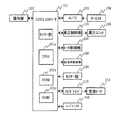
次に、画像形成装置の電源への給電経路を接続する電源スイッチ、及び電源スイッチのオン/オフ状態の検知について、図4を用いて説明する。 Next, the power switch for connecting the power supply path to the power source of the image forming apparatus and the detection of the on / off state of the power switch will be described with reference to FIG.
図4は、画像形成装置の電源制御関係の概略ブロック図である。図4において、301は電源スイッチであり、ユーザによってオン/オフ操作が行われる。また、302はリレーであり、電源スイッチ301と並列接続になるように構成され、システムコントローラ101によって、短絡又は開放状態に制御される。
FIG. 4 is a schematic block diagram of the power supply control relationship of the image forming apparatus. In FIG. 4,
そして、画像形成装置は、電源スイッチ301がユーザによってオフ操作された場合でも、リレー302を短絡させることにより商用電源からの給電を持続させ、画像形成装置への給電が即時遮断されないように、電源供給制御を行っている。例えば、図2に示したハードディスク112へのアクセス中に、突然電源が遮断されてしまうと、ハードディスクの内容が破損されてしまう虞があるため、ハードディスクのアクセスが終了するまでの所定時間だけ給電が保持されている。
Then, even when the
画像形成装置への電源の給電を保持する回路構成について、図4を用いて説明する。 A circuit configuration for holding power supply to the image forming apparatus will be described with reference to FIG.
画像形成装置は、電源スイッチがオフ操作された場合でも、システムコントローラ101からの制御信号Sig2に基づいて、リレー302を短絡状態にすることにより、画像形成装置の電源201への給電を維持する。
Even when the power switch is turned off, the image forming apparatus maintains power supply to the
そして、電源スイッチ301のオン/オフ状態は検知回路202によって検知され、システムコントローラ101は、検知回路202から送信され、電源スイッチ301のオン/オフ状態を通知する検知信号Sig3を常に監視している。
The on / off state of the
システムコントローラ101は、検知信号Sig3により、電源スイッチ301がオフ操作されたことを検知すると、ハードディスク112へのアクセス処理を終了させて、電源をオフできる状態に移行させる。電源をオフできる状態に移行させた後に、システムコントローラ101は、リレー302を開放するように制御信号Sig2を変化させ、画像形成装置への給電を遮断させる。
When the
電源スイッチ301は、端子1と端子2との間を接続、又は遮断する第1のスイッチ301a、及び、端子3と端子4との間を接続、又は遮断する第2のスイッチ301bの2つのスイッチを有する電源スイッチである。この2つのスイッチは同一パッケージに実装され、ユーザが操作できるのはスイッチ301aであり、スイッチ301bはユーザがスイッチ301aを操作することに連動してほぼ同時にオン/オフされる。また、この電源スイッチ301は、大電流用接点のみを備えたものである。大電流用接点には、一般的に銀、又は銀合金が使用され、本実施形態例の接点においても、銀が用いられている。銀、又は銀合金を使用した接点は、経時変化や周囲環境によっては、空気中の硫黄と化合して接点表面に硫化銀のような硫化皮膜ができやすく、その結果、接触抵抗が大きくなり、接触不良につながる不具合が生じる。しかし、接点表面の硫化皮膜は、接点が閉じる際に流れる大電流のラッシュ電流によって破壊することができる。
The
しかし、接点に流れる電流値が微小な場合には、その破壊効果は期待できない。そのため、電源スイッチ301がオン状態に操作されても、接点表面の硫化皮膜が破壊されず、接点部においては接触不良により非導通状態のままとなり、電源201への給電がされなくなる虞がある。従って、大電流用接点を備えた電源スイッチに、微小な電流しか流さないことは望ましくない。
However, when the value of the current flowing through the contact is very small, the destruction effect cannot be expected. Therefore, even if the
その一方、電源スイッチのオン/オフ状態を検出する検知回路202に、大電流を流すことは好ましくない。なぜなら、電源スイッチのオン/オフ状態は微小電流で検知可能であり、検知回路202に大電流を流すほど、無駄な消費電流を発生させてしまうことになり、装置の低電力化を妨げることになるからである。
On the other hand, it is not preferable to flow a large current through the
そこで、本実施形態例では、検知回路202に流す電流値を微小に留めながら、電源スイッチ301の接点表面に硫化膜が形成されても、それを破壊できる電源スイッチ回路を、以下のように構成している。
Therefore, in this embodiment, a power switch circuit that can destroy a sulfide film formed on the contact surface of the
まず、回路構成について説明する。 First, the circuit configuration will be described.
図4において、スイッチ301aの一端(端子2側)とスイッチ301bの一端(端子3側)とを直列に接続する。そして、スイッチ301aの他端(端子1側)を商用電源に接続し、スイッチ301bの他端(端子4側)を画像形成装置の電源201に接続する。さらに、スイッチ301aとスイッチ301bの接続点(端子2と端子3の接続点)を、検知回路202に接続する。
In FIG. 4, one end (terminal 2 side) of the
次に、回路動作について説明する。 Next, circuit operation will be described.
電源スイッチ301がオフの状態では、電源201を始め、検知回路202、システムコントローラ101等が全て非通電状態であるため、リレー302もオフ状態(開放状態)である。そして、電源スイッチ301をオン操作すると、2つのスイッチ301a、301bがオンされ、スイッチ301a,301bを経由して、商用電源から電源201へ電流が流れ込む。この電源スイッチ301のオン操作により流れ込む電流は、後述するように、電源スイッチ301の接点に硫化皮膜が発生していても、それを破壊するのに十分なものである。
When the
図5は、本実施形態例の画像形成装置の電源部における商用電源入力部の概略構成図である。図5に示すように、電源201の商用電源入力部は、商用電源を全波整流するダイオードブリッジ801と、その後段に平滑コンデンサ802とを備えており、本実施形態例では、平滑コンデンサ802の容量は680μFである。そして、電源スイッチ301のオン操作時には、商用電源から電源スイッチ301を経由して平滑コンデンサ802が充電されるので、充電のための大電流が電源スイッチ301の接点に流れる。
FIG. 5 is a schematic configuration diagram of a commercial power input unit in the power unit of the image forming apparatus according to the present exemplary embodiment. As shown in FIG. 5, the commercial power input unit of the
図6は、本実施形態例において、電源スイッチ301がオン操作された時に、電源スイッチ301を流れる電流波形の一例を示す図である。図6より、電源スイッチ301の接点には、ピーク値で80A(アンペア)程度の電流が流れていることが分かる。なお、電源スイッチ301の大電流用接点材料である銀の硫化皮膜を破壊するためには、数A程度の電流を流せば十分である。
FIG. 6 is a diagram illustrating an example of a waveform of a current flowing through the
以上説明したように、電源スイッチ301及び電源201の接続を図4に示す回路構成にすることで、電源スイッチ301の接点表面に硫化皮膜が形成されても、それを破壊することを可能にしている。
As described above, by connecting the
また、本実施形態例においては、検知回路202は図7に示すように構成されている。図7において、抵抗501は、検知回路202に流れる電流を制限する抵抗であり、本実施形態例では、その抵抗値を100kΩとしている。
In this embodiment, the
従って、スイッチ301aとスイッチ301bの接続点から検知回路202へと流れる電流I、及び検知回路202における電力損失の概算値は、商用電源を100Vとすると以下のとおりである。
電流I=V(電圧)/R(抵抗)
=100(V)/100(kΩ)
=1(mA)
電力損失Pw=V(電圧)×I(電流)
=100(V)×1(mA)
=0.1W
本実施形態例では、フォトカプラ502の動作に必要な電流が約1mAであるので、抵抗501は上記のような抵抗値としている。
Therefore, the current I flowing from the connection point of the
Current I = V (voltage) / R (resistance)
= 100 (V) / 100 (kΩ)
= 1 (mA)
Power loss Pw = V (voltage) x I (current)
= 100 (V) x 1 (mA)
= 0.1W
In this embodiment, since the current required for the operation of the
スイッチ301aとスイッチ301bの接続点から検知回路202へと流れる電流は1mAしかないため、この微小電流だけでは電源スイッチ301の接点上に形成された硫化皮膜を破壊する能力を有していない。即ち、検知回路202へは酸化皮膜を破壊できるような大電流は流れない。
Since the current flowing from the connection point of the
なお、上記電力損失は電源スイッチ301がオン状態では常に発生するため、このような電力損失は可能な限り小さくすることが望ましい。例えば、検知回路202に流れる電流によっても、電源スイッチ301の接点上に形成された硫化皮膜を破壊させようとして、検知回路202に流れる電流値を1Aに設定した場合の電力損失Pw2は
電力損失Pw2=100(V)×1(A)=100W
となり、非常に大きな電力損失が発生してしまうため、なおさら望ましくない。
Since the power loss always occurs when the
And a very large power loss occurs, which is even more undesirable.
また、検知回路202からシステムコントローラに送信される検知信号Sig3については、電源スイッチ301の状態に応じて、次のように変化する。
The detection signal Sig3 transmitted from the
電源スイッチ301がオン状態の場合には、スイッチ301aとスイッチ301bの接続点を経由して、検知回路202内のフォトカプラ502に電流が流れる。その結果、検知信号Sig3は、図8(a)に示すように、商用電源の交流電圧が0V(ボルト)になるゼロクロス付近を除いて、Lowレベルの信号となる。一方、ゼロクロスでは、交流電圧が0Vになるため、フォトカプラ502には電流が流れず、検知信号Sig3はHighレベルとなる。
When the
また、電源スイッチ301がオフ状態の場合には、フォトカプラ502に電流が流れないために、検知信号Sig3は図8(b)に示すように、常時Highレベルの信号となる。システムコントローラ101は、このように変化する検知信号Sig3を受信することによって、電源スイッチ301のオン/オフ状態を判別している。
When the
以上説明したように、本実施形態例においては、検知回路202に流れる電流の電流値を微小に留めながら、電源スイッチ301の接点表面に硫化皮膜が形成されても、それを破壊できる回路構成を実現している。
As described above, the present embodiment has a circuit configuration that can destroy the sulfide film even if a sulfide film is formed on the contact surface of the
図9は、本実施形態例における画像形成装置の電源への給電の保持、遮断の制御シーケンスを示すフローチャートである。以下の制御シーケンスは、システムコントローラ101に実装されたROM101b内に格納されたプログラムに基づいて、システムコントローラ101に実装されたCPU101aによって実行される。
FIG. 9 is a flowchart illustrating a control sequence for holding and shutting off the power supply to the power source of the image forming apparatus according to the present exemplary embodiment. The following control sequence is executed by the
電源スイッチ301がオン操作されると、システムコントローラ101が起動され(S701)、画像形成動作に必要な各種の設定、動作を順次、開始する。
When the
これら画像形成に必要な動作に先行して、システムコントローラ101は、制御信号Sig2を出力し、商用電源から画像形成装置の電源への給電ラインを保持するリレー302を短絡する(S702)。
Prior to these operations necessary for image formation, the
これにより、電源スイッチ301がオフ操作されても、システムコントローラ101によって画像形成装置の電源のオフできる状態になるまで、商用電源からの電源供給を維持することができる。
Thus, even if the
そして、画像形成装置のシステムコントローラ101は、一定周期のポーリングにより、電源スイッチ301のオン/オフ状態を示す検知信号Sig3を監視する(S703)。
Then, the
検知信号Sig3がHighレベルになり、電源がオフされたことが検知された場合には、システムコントローラ101は、画像形成装置の電源を直ちに遮断してもよい状態か否かを判断する(S704)。例えば、システムコントローラ101がハードディスクへアクセスしている最中であれば、即座に電源を遮断することができないため、ハードディスクへのアクセスを中止し、電源をオフするための準備を行う(S705)。
When the detection signal Sig3 becomes High level and it is detected that the power is turned off, the
例えば、ハードディスクへのアクセスが完了し、電源を遮断してもよい状態であれば(S704)、リレー302を開放状態にする(S706)。これによって、画像形成装置は電源がオフされた状態となる。
For example, if the access to the hard disk is completed and the power supply can be shut off (S704), the
以上説明したようにして、本発明によれば、廉価な大電流用の電源スイッチを用いて、画像形成装置の電源への給電及び遮断を行うと同時に、電源スイッチがオン又はオフされたことを微小電流にて検知するようにすることができる。これにより、画像形成装置の消費電力の低減と、電源スイッチのコスト低減とを実現させることができる。 As described above, according to the present invention, a power switch for an image forming apparatus is powered on and off using an inexpensive high-current power switch, and at the same time, the power switch is turned on or off. Detection can be performed with a minute current. Thereby, it is possible to reduce the power consumption of the image forming apparatus and reduce the cost of the power switch.
101 システムコントローラ
201 電源
202 検知回路
301 電源スイッチ
302 リレー
101
Claims (8)
前記電源スイッチと並列に設けられ、短絡又は開放状態に制御されるリレーと、
前記電源スイッチのオン/オフ状態を検知する検知回路と、
前記検知回路で生成された検知信号に基づいて、前記リレーを短絡又は開放状態に制御する制御手段と、
を備え、
前記電源スイッチは、第1のスイッチ及び前記第1のスイッチに連動する第2のスイッチを有し、前記第1のスイッチと前記第2のスイッチとが直列に接続され、前記第1のスイッチの他端は前記商用電源に接続され、前記第2のスイッチの他端は前記電源装置に接続され、前記第1のスイッチと前記第2のスイッチとの接続点が、前記検知回路に接続されていることを特徴とする電源供給制御装置。 A power switch that switches between an on state that connects a power supply path from a commercial power source to a power supply device and an off state that blocks a power supply path from the commercial power source to the power supply device;
A relay provided in parallel with the power switch and controlled to a short circuit or an open state;
A detection circuit for detecting an on / off state of the power switch;
Based on the detection signal generated by the detection circuit, the control means for controlling the relay to a short circuit or an open state;
With
The power switch includes a first switch and a second switch interlocked with the first switch, and the first switch and the second switch are connected in series, and the first switch The other end is connected to the commercial power supply, the other end of the second switch is connected to the power supply device, and a connection point between the first switch and the second switch is connected to the detection circuit. A power supply control device characterized by comprising:
前記検知回路は、前記商用電源から前記第1のスイッチと前記第2のスイッチとの接続点を経由して電流が流れる抵抗を有し、前記接続点から前記検知回路へ流れる電流が前記硫化皮膜を破壊しない電流値となるように前記抵抗の抵抗値が設定されていることを特徴とする請求項1に記載の電源供給制御装置。 The current flowing from the commercial power source to the power supply device via the first switch and the second switch is a current having a current value that destroys the sulfide film formed on the contact surface of the power switch,
The detection circuit includes a resistor through which a current flows from the commercial power source via a connection point between the first switch and the second switch, and a current flowing from the connection point to the detection circuit is the sulfide film. The power supply control device according to claim 1 , wherein a resistance value of the resistor is set so as to have a current value that does not destroy the power supply.
前記検知回路から前記電源スイッチがオフ状態であることを示す検知信号を受信した場合には、電源をオフするための処理を行った後、前記リレーを開放し、前記商用電源と前記電源装置との給電経路の接続を遮断することを特徴とする請求項1ないし3のいずれか1項に記載の電源供給制御装置。 When the control means receives a detection signal indicating that the power switch is in an ON state from the detection circuit, the control means short-circuits the relay and maintains a power supply path connection between the commercial power supply and the power supply device. And
Wherein when the power supply switch from the detection circuit receives a detection signal indicating the OFF state, after the processing for turning off the power, opening the relay, the commercial power source and the power supply device 4. The power supply control device according to claim 1, wherein the power supply path is disconnected from the power supply path.
前記電源をオフするための処理は、前記制御手段が前記ハードディスクに対するアクセスを完了させる処理であることを特徴とする請求項4に記載の電源供給制御装置。 Have a hard disk to record information,
The power supply control apparatus according to claim 4, wherein the process for turning off the power is a process in which the control unit completes access to the hard disk.
Priority Applications (1)
| Application Number | Priority Date | Filing Date | Title |
|---|---|---|---|
| JP2010098801A JP5460442B2 (en) | 2010-04-22 | 2010-04-22 | Power supply control device and image forming apparatus |
Applications Claiming Priority (1)
| Application Number | Priority Date | Filing Date | Title |
|---|---|---|---|
| JP2010098801A JP5460442B2 (en) | 2010-04-22 | 2010-04-22 | Power supply control device and image forming apparatus |
Publications (3)
| Publication Number | Publication Date |
|---|---|
| JP2011227378A JP2011227378A (en) | 2011-11-10 |
| JP2011227378A5 JP2011227378A5 (en) | 2013-05-23 |
| JP5460442B2 true JP5460442B2 (en) | 2014-04-02 |
Family
ID=45042755
Family Applications (1)
| Application Number | Title | Priority Date | Filing Date |
|---|---|---|---|
| JP2010098801A Expired - Fee Related JP5460442B2 (en) | 2010-04-22 | 2010-04-22 | Power supply control device and image forming apparatus |
Country Status (1)
| Country | Link |
|---|---|
| JP (1) | JP5460442B2 (en) |
Families Citing this family (5)
| Publication number | Priority date | Publication date | Assignee | Title |
|---|---|---|---|---|
| JP5880023B2 (en) * | 2011-12-22 | 2016-03-08 | 株式会社リコー | Power supply circuit, image forming apparatus |
| JP6026452B2 (en) * | 2014-02-28 | 2016-11-16 | 京セラドキュメントソリューションズ株式会社 | Image forming apparatus |
| JP6092137B2 (en) * | 2014-02-28 | 2017-03-08 | 京セラドキュメントソリューションズ株式会社 | Image forming apparatus |
| JP2020148951A (en) * | 2019-03-14 | 2020-09-17 | 株式会社沖データ | Power supply device and image forming device |
| JP7452075B2 (en) | 2020-02-19 | 2024-03-19 | 京セラドキュメントソリューションズ株式会社 | Switch status detection device, image forming device |
Family Cites Families (8)
| Publication number | Priority date | Publication date | Assignee | Title |
|---|---|---|---|---|
| JPH0564352A (en) * | 1991-09-05 | 1993-03-12 | Ricoh Co Ltd | Safety protection circuit |
| JPH0667486A (en) * | 1992-08-24 | 1994-03-11 | Canon Inc | Image forming device |
| JPH07226815A (en) * | 1994-02-15 | 1995-08-22 | Ricoh Co Ltd | Communication equipment and image-forming device with this equipment |
| JPH08202233A (en) * | 1995-01-23 | 1996-08-09 | Canon Inc | Image forming device |
| JPH0951991A (en) * | 1995-08-14 | 1997-02-25 | Elna Co Ltd | Electric razor |
| JP2002116668A (en) * | 2000-10-04 | 2002-04-19 | Ricoh Co Ltd | Door switch unit |
| JP2006044228A (en) * | 2004-07-09 | 2006-02-16 | Ricoh Co Ltd | Image forming device |
| JP4520275B2 (en) * | 2004-10-25 | 2010-08-04 | Hoya株式会社 | Laser light source device |
-
2010
- 2010-04-22 JP JP2010098801A patent/JP5460442B2/en not_active Expired - Fee Related
Also Published As
| Publication number | Publication date |
|---|---|
| JP2011227378A (en) | 2011-11-10 |
Similar Documents
| Publication | Publication Date | Title |
|---|---|---|
| US8983314B2 (en) | Image forming apparatus capable of detecting contact fusion, and relay control apparatus | |
| US9081340B2 (en) | Image forming apparatus having first and second cooling portions or fans cooling end regions of a fixing portion with respect to a direction perpendicular to a recording material conveyance direction | |
| CN100568119C (en) | Fixing device | |
| JP2006085138A (en) | Color image forming apparatus and image forming method | |
| JP5460442B2 (en) | Power supply control device and image forming apparatus | |
| US7965951B2 (en) | Image recording apparatus having a lower fixing temperature | |
| US9348285B2 (en) | Image forming apparatus | |
| US6957022B2 (en) | Image forming apparatus | |
| JP2010054688A (en) | Temperature control device and control method | |
| US20060245768A1 (en) | Image forming apparatus | |
| US6907217B2 (en) | Image forming device capable of suppressing distortion in output image | |
| JP2000330426A (en) | Electrophotographic device | |
| JP2004354983A (en) | Image heating device with mechanism for preventing winding of recording medium around fixing rotor | |
| JP5037918B2 (en) | Image forming apparatus | |
| JP2004148724A (en) | Mechanism for detecting opening/closing of cover | |
| JP2009300518A (en) | Electronic device | |
| JP2007309982A (en) | Image fixing device | |
| JP2012226048A (en) | Image forming apparatus | |
| US11841665B2 (en) | Image forming apparatus | |
| JP2007309988A (en) | Fixing device | |
| JP2011033808A (en) | Image forming apparatus | |
| JP5558947B2 (en) | Image forming apparatus | |
| US20240201627A1 (en) | Image forming apparatus | |
| JPH11184184A (en) | Image forming device | |
| JP2021004938A (en) | Image forming apparatus |
Legal Events
| Date | Code | Title | Description |
|---|---|---|---|
| RD03 | Notification of appointment of power of attorney |
Free format text: JAPANESE INTERMEDIATE CODE: A7423 Effective date: 20120208 |
|
| A521 | Request for written amendment filed |
Free format text: JAPANESE INTERMEDIATE CODE: A523 Effective date: 20130416 |
|
| A621 | Written request for application examination |
Free format text: JAPANESE INTERMEDIATE CODE: A621 Effective date: 20130416 |
|
| A977 | Report on retrieval |
Free format text: JAPANESE INTERMEDIATE CODE: A971007 Effective date: 20131213 |
|
| TRDD | Decision of grant or rejection written | ||
| A01 | Written decision to grant a patent or to grant a registration (utility model) |
Free format text: JAPANESE INTERMEDIATE CODE: A01 Effective date: 20131217 |
|
| A61 | First payment of annual fees (during grant procedure) |
Free format text: JAPANESE INTERMEDIATE CODE: A61 Effective date: 20140114 |
|
| LAPS | Cancellation because of no payment of annual fees |