JP5452040B2 - Optical information reproducing method, optical head, and optical disc apparatus - Google Patents
Optical information reproducing method, optical head, and optical disc apparatus Download PDFInfo
- Publication number
- JP5452040B2 JP5452040B2 JP2009060420A JP2009060420A JP5452040B2 JP 5452040 B2 JP5452040 B2 JP 5452040B2 JP 2009060420 A JP2009060420 A JP 2009060420A JP 2009060420 A JP2009060420 A JP 2009060420A JP 5452040 B2 JP5452040 B2 JP 5452040B2
- Authority
- JP
- Japan
- Prior art keywords
- light
- optical
- path length
- optical path
- signal
- Prior art date
- Legal status (The legal status is an assumption and is not a legal conclusion. Google has not performed a legal analysis and makes no representation as to the accuracy of the status listed.)
- Expired - Fee Related
Links
Images


Classifications
-
- G—PHYSICS
- G11—INFORMATION STORAGE
- G11B—INFORMATION STORAGE BASED ON RELATIVE MOVEMENT BETWEEN RECORD CARRIER AND TRANSDUCER
- G11B7/00—Recording or reproducing by optical means, e.g. recording using a thermal beam of optical radiation by modifying optical properties or the physical structure, reproducing using an optical beam at lower power by sensing optical properties; Record carriers therefor
- G11B7/004—Recording, reproducing or erasing methods; Read, write or erase circuits therefor
- G11B7/005—Reproducing
-
- G—PHYSICS
- G11—INFORMATION STORAGE
- G11B—INFORMATION STORAGE BASED ON RELATIVE MOVEMENT BETWEEN RECORD CARRIER AND TRANSDUCER
- G11B7/00—Recording or reproducing by optical means, e.g. recording using a thermal beam of optical radiation by modifying optical properties or the physical structure, reproducing using an optical beam at lower power by sensing optical properties; Record carriers therefor
- G11B7/08—Disposition or mounting of heads or light sources relatively to record carriers
- G11B7/09—Disposition or mounting of heads or light sources relatively to record carriers with provision for moving the light beam or focus plane for the purpose of maintaining alignment of the light beam relative to the record carrier during transducing operation, e.g. to compensate for surface irregularities of the latter or for track following
- G11B7/0941—Methods and circuits for servo gain or phase compensation during operation
-
- G—PHYSICS
- G11—INFORMATION STORAGE
- G11B—INFORMATION STORAGE BASED ON RELATIVE MOVEMENT BETWEEN RECORD CARRIER AND TRANSDUCER
- G11B7/00—Recording or reproducing by optical means, e.g. recording using a thermal beam of optical radiation by modifying optical properties or the physical structure, reproducing using an optical beam at lower power by sensing optical properties; Record carriers therefor
- G11B7/12—Heads, e.g. forming of the optical beam spot or modulation of the optical beam
- G11B7/135—Means for guiding the beam from the source to the record carrier or from the record carrier to the detector
- G11B7/1359—Single prisms
-
- G—PHYSICS
- G11—INFORMATION STORAGE
- G11B—INFORMATION STORAGE BASED ON RELATIVE MOVEMENT BETWEEN RECORD CARRIER AND TRANSDUCER
- G11B7/00—Recording or reproducing by optical means, e.g. recording using a thermal beam of optical radiation by modifying optical properties or the physical structure, reproducing using an optical beam at lower power by sensing optical properties; Record carriers therefor
- G11B2007/0003—Recording, reproducing or erasing systems characterised by the structure or type of the carrier
- G11B2007/0009—Recording, reproducing or erasing systems characterised by the structure or type of the carrier for carriers having data stored in three dimensions, e.g. volume storage
- G11B2007/0013—Recording, reproducing or erasing systems characterised by the structure or type of the carrier for carriers having data stored in three dimensions, e.g. volume storage for carriers having multiple discrete layers
Description
本発明は、光ディスク装置の再生信号の高S/N化に関する。 The present invention relates to a high S / N ratio of a reproduction signal of an optical disc apparatus.
光ディスクは、青色半導体レーザと、高NA対物レンズを用いるブルーレイディスクの製品化に至って、光学系の分解能としてはほぼ限界に達し、さらなる大容量化に向けては、今後、記録層の多層化が有力となると考えられる。このような多層光ディスクにおいては各記録層からの検出光量がほぼ同等となる必要性から、特定の記録層からの反射率は小さくせざるを得ない。ところが光ディスクは大容量化とともにビデオなどのダビング速度の高速化の必要性から、データ転送速度の高速化も続いており、そのままでは再生信号のS/N比が十分確保できなくなりつつある。したがって今後の記録層の多層化と高速化を同時に進めていくためには、検出信号の高S/N化が必須となる。 Optical discs have reached the limit of optical system resolution, resulting in the production of Blu-ray Discs that use blue semiconductor lasers and high NA objective lenses. To further increase the capacity, the number of recording layers will increase in the future. It is thought to be influential. In such a multi-layer optical disc, the reflectance from a specific recording layer must be reduced because the amount of light detected from each recording layer needs to be substantially equal. However, since the optical disk needs to have a large capacity and a high dubbing speed for video and the like, the data transfer speed is also increasing, and the S / N ratio of the reproduced signal cannot be secured sufficiently. Therefore, in order to proceed with the multilayering and speeding up of the recording layer in the future at the same time, it is essential to increase the S / N of the detection signal.
光ディスクの再生信号の高S/N化に関する技術は、たとえば特許文献1、特許文献2,特許文献3などに述べられている。特許文献1、特許文献2は光磁気ディスクの再生信号の高S/N化に関して、半導体レーザからの光を光ディスクに照射する前に分岐して、光ディスクに照射しない光を、光ディスクからの反射光と合波して干渉させることにより、微弱な信号の振幅を、光ディスクに照射しない光の光量を大きくすることによって増幅することを狙ったものである。光磁気ディスクの信号検出で従来用いられている偏光ビームスプリッタの透過光と反射光の差動検出では、本質的にはもとの入射偏光成分と光磁気ディスクによる偏光回転によって生じる入射偏光方向と直交する偏光成分を干渉させて、入射偏光で直交偏光成分を増幅して検出を行なうことになっている。したがって、もとの入射偏光成分を増大させれば信号を増大させることができるが、光ディスクに入射させる光強度は、データを消去したり上書きしたりしないようにするために、ある程度以下に抑える必要がある。
For example,
これに対して上記従来の技術では、予め信号光と干渉させる光を分離しておいて、これをディスクに集光せずに信号光と干渉させ、信号増幅のため干渉させる光の強度を、ディスク表面の光強度と関係なく強くできるようにしているのである。これにより原理的には光強度の許す範囲で、強度を強くすればするほど、光検出器からの光電流を電圧変換するアンプのノイズに比べたS/N比を高めることができる。特許文献3ではフォトクロミック媒体を用いた光ディスクの再生信号の高S/N化に関し,参考文献1,参考文献2と同様に,光ディスクに照射しない光を,光ディスクからの反射光と干渉させることによって信号増幅を狙っている。フォトクロミック媒体を用いた光ディスクについても,信号再生のため入射光強度が高い程媒体の劣化を早めるため,上記光磁気ディスクと同様に記録媒体に照射する光の強度に制限を伴う。
On the other hand, in the above conventional technique, the light to be interfered with the signal light is separated in advance, and this is interfered with the signal light without condensing it on the disk, and the intensity of the light to be interfered for signal amplification is This makes it possible to increase the intensity regardless of the light intensity on the disk surface. As a result, in principle, the S / N ratio compared to the noise of the amplifier that converts the photocurrent from the photodetector into a voltage can be increased as the intensity is increased within the allowable range of the light intensity.
特許文献1では、2つの光を干渉させて干渉光強度を検出している。この際、干渉させるディスク反射光の光路長を可変とし、干渉信号振幅の確保を狙っている。特許文献2,特許文献3,特許文献4では干渉光強度検出に加えて、差動検出も行っている。これにより信号に寄与しない各光の強度成分をキャンセルし、信号振幅を2倍にすることで高S/N化を図っている。
In
一般に、2つの光の干渉により得られる干渉信号は、干渉させる二つの光の間の位相差(光路長差)に依存する。これに対し、特許文献1では光路中に挿入された三角プリズムを入射光軸方向に可動とすることで光路長差の安定化を図っている。同様に、特許文献4では干渉光学系全体を光ディスクに追従させることで、光ディスクの回転に伴う面ぶれにより発生する光路長差をキャンセルすることを図っている。また、光ディスクに当てない光を反射するミラーの位置を光軸方向に可動とすることで光路長差の安定化を図っている。光路長差を特許文献5では互いに干渉状態の異なる複数の干渉信号を生成し、それらの演算により信号を生成することで、上記位相差に依存しない増幅信号を出力することを図っている。
In general, an interference signal obtained by interference between two lights depends on a phase difference (optical path length difference) between the two lights to be interfered. On the other hand,
上記従来技術において、干渉信号を安定に保つには、現在の光ディスクの面ぶれ約600μmに対し、可動とする対象物を追従させ、更に信号光と参照光の位相差を固定する、すなわち光源の波長よりも十分小さい数nm程度の精度で位置決めを行う必要がある。しかし現在のアクチュエータでこの要求に見合うストロークと位置決め精度を達成することは非常に難しい。更に、光ディスクに設けられたカバー層の厚みのむらも光路長差を乱す原因となるが、上記従来技術においてこの厚みのむさらに対応する光路長の制御方法については特に述べられていない。 In the above-described prior art, in order to keep the interference signal stable, the movable object is made to follow the current optical disc surface shake of about 600 μm, and the phase difference between the signal light and the reference light is fixed. It is necessary to perform positioning with an accuracy of about several nanometers sufficiently smaller than the wavelength. However, it is very difficult to achieve a stroke and positioning accuracy that meet this requirement with current actuators. Furthermore, unevenness in the thickness of the cover layer provided on the optical disk also causes the optical path length difference to be disturbed. However, in the above-described prior art, a method for controlling the optical path length corresponding to this uneven thickness is not particularly described.
これに対し、特許文献5では光路長差に依存しない出力を得る方法を採っているため上記の問題は発生しないが、光路長差に依存しない出力を得るための信号処理過程において非線形演算などの複雑な演算処理が要求されるため、信号処理回路への負担が大きくなる。また、複数の干渉信号から光路長差に依存しない出力するため、各干渉信号に混入する熱雑音が加算されてノイズが増加したり、演算処理の不完全性によりノイズが混入したりすることにより、上記演算処理が信号品質を劣化させる要因になる。更に、光路長差に依存しない出力を得るためには、光学系の各種パラメータに高い精度が要求され、光学系の構築が非常に困難になる。
On the other hand,
上記課題に鑑み、本発明の第1の目的は、2つの光の光路差の調整が容易で、信号増幅効果が高く、光学系の小型化に適した、干渉型の光情報信号の再生方法を提供することにある。 In view of the above problems, a first object of the present invention is to provide an interference-type optical information signal reproduction method that can easily adjust the optical path difference between two lights, has a high signal amplification effect, and is suitable for downsizing an optical system. Is to provide.
本発明の第2の目的は、2つの光の光路差の調整が容易で、信号増幅効果が高く、光学系の小型化に適した、干渉型の光情報信号の検出系を備えた光ヘッドを提供することである。 A second object of the present invention is to provide an optical head equipped with an interference type optical information signal detection system that can easily adjust an optical path difference between two lights, has a high signal amplification effect, and is suitable for downsizing of an optical system. Is to provide.
本発明の第3の目的は、2つの光の光路差の調整が容易で、信号増幅効果が高く、光学系の小型化に適した、干渉型の光情報信号の検出系を備えた光ディスク装置を提供することである。 A third object of the present invention is to provide an optical disc apparatus equipped with an interference type optical information signal detection system that can easily adjust an optical path difference between two lights, has a high signal amplification effect, and is suitable for downsizing of an optical system. Is to provide.
本発明では、信号光と参照光の干渉光を複数の検出器で検出することにより再生信号を取得する方式の光ディスク装置、光ヘッドあるいは光学的情報再生方法において、光ヘッド内に形成される光路長の調整を、光路長差の粗調整、微調整および光路長差固定位置調整の3つに分けて実行することにより前述の課題を解決する。光路長差の粗調整とは、光ヘッドと光情報記録媒体との相対間隔の変動(例えば光ディスクの面ぶれなど)に基づき発生する信号光と参照光との光路差をキャンセルするための調整のことを指す。光路差の微調整および光路長差固定位置調整の定義については後述する。 According to the present invention, an optical path formed in an optical head in an optical disk apparatus, an optical head, or an optical information reproducing method of a type in which a reproduction signal is obtained by detecting interference light of signal light and reference light with a plurality of detectors. The above-described problem is solved by performing the length adjustment in three parts: coarse adjustment of the optical path length difference, fine adjustment, and optical path length difference fixed position adjustment. The rough adjustment of the optical path length difference is an adjustment for canceling the optical path difference between the signal light and the reference light, which is generated based on fluctuations in the relative distance between the optical head and the optical information recording medium (for example, optical disc surface shake). Refers to that. The definition of the fine adjustment of the optical path difference and the adjustment of the optical path length difference fixed position will be described later.
なお、以上述べた光路長の微調整、光路長差固定位置調整および光路差粗調整は、概念としては区別されるが、各調整が同一の機構で実施される形態もある。 Note that the fine adjustment of the optical path length, the optical path length difference fixed position adjustment, and the optical path difference coarse adjustment described above are distinguished in concept, but there is a form in which each adjustment is implemented by the same mechanism.
従来のディスク装置と同等のサイズで作製可能で、信号増幅効果が高く、安価な干渉型の光ディスク装置、光ヘッドおよび信号再生方法が実現される。 An interference type optical disc device, an optical head, and a signal reproducing method that can be manufactured in the same size as a conventional disc device, have a high signal amplification effect, and are inexpensive are realized.
以下、図1を用いて本発明の実施形態を説明する。 Hereinafter, an embodiment of the present invention will be described with reference to FIG.
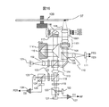
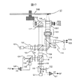
図1は本実施例の光ディスク装置の全体構成例を示す。図1に示す光ディスク装置は、大まかには、光ディスク109を保持するスピンドルモータ77を含むディスク支持手段、光ディスク109へ各種のデータを入出力する光ヘッド(光ピックアップ)2001、光ディスク装置全体の動作を制御するファームウェアが動作するマイクロプロセッサ27、光ヘッドの再生信号に各種の処理を行う再生信号処理ブロック2、各種制御用パラメータや制御用のテーブルなどが格納されるメモリ29、光ヘッド2001に搭載されたレーザを駆動するレーザドライバ28、光ヘッドから光ディスクに照射される光スポット37の位置制御を行うサーボ回路79、光ヘッド2001の位置を制御することなどにより光ディスク109の所定の位置に光スポット37を移動させる自動位置制御手段76などにより構成される。
次に、光ヘッド2001の内部構成およびその機能について説明する。以下に説明する光ヘッド系を構成する各光学素子は、光学モジュールとして一体形成されている。本実施例の光ヘッド光学系は、レーザ光から放出された光を光ディスクに導き反射させ、当該反射光と参照信号とを干渉させて干渉光を生成するための干渉光学系と、生成された干渉光を分離し、分離された各々の干渉光に位相差を付与して複数の検出器で検出するための検出光学系とにより構成される。
FIG. 1 shows an example of the overall configuration of the optical disk apparatus of the present embodiment. The optical disk apparatus shown in FIG. 1 roughly includes disk support means including a
Next, the internal configuration and function of the
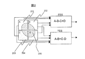
まず、干渉光学系の詳細について説明する。半導体レーザ101からの光をコリメートレンズ102によって平行光として、λ/2板103を透過させて偏光ビームスプリッタ104に入射させる。偏光ビームスプリッタ104は分離面に入射するp偏光(以後、水平偏光と呼ぶ)をほぼ100%透過し、s偏光(以後、垂直偏光と呼ぶ)をほぼ100%反射させる機能、すなわち透過光と反射光とを分離する機能を有している。このとき、λ/2板103の光軸のまわりの回転角度を調整することにより、透過光と反射光の強度比を調整することができる。透過する光は特殊偏光ビームスプリッタ105に入射する。特殊偏光ビームスプリッタ105は水平偏光を100%透過し、垂直偏光の一部を反射、一部を透過するという性質を持っている。このため入射した光は100%透過し、λ/4板106を透過して円偏光に変換され、球面収差を補正するビームエキスパンダ1101を通過し、2次元アクチュエータ107に搭載された対物レンズ108により、光ディスク109上の記録層に集光される。光ディスクからの反射光(以後、信号光と呼ぶ)は同じ光路を戻り、対物レンズ108によって平行光とされ、λ/4板106を再び通過することにより最初に入射したときとは90°偏光方向が回転した直線偏光となる。次に特殊偏光ビームスプリッタ105に入射し、上記の性質により一部が透過、一部が反射する。反射光はシリンドリカルレンズ110によって検出器111に入射する。ここで検出器111は図2のように検出器201,202,203,204の4つに分割されており、図のようにそれぞれの出力信号をA,B,C,Dとおくと、演算A-B-C+Dが焦点ずれ信号(FES)、演算A-B+C-Dがトラックずれ信号(TES)、としてそれぞれ出力され、2次元アクチュエータ107のボイスコイルモータに電流としてフィードバックされる。このため、図2に示す検出器111は、演算A-B-C+Dおよび演算A-B+C-Dを実行するための論理演算回路を備えている。
First, details of the interference optical system will be described. Light from the
一方、特殊偏光ビームスプリッタ105を透過した光は偏光ビームスプリッタ104に入射する。すると偏光が90度回転しているため、反射して集光レンズ113に入射する(以後、本反射光を参照光と呼ぶ)。一方、半導体レーザ101から出射し、偏光ビームスプリッタ104で反射された光は可動部114に搭載された反射プリズム115において反射し、2次元アクチュエータ107上に搭載されたコーナーキューブプリズム116に入射する。コーナーキューブプリズム116は入射した光を正反対の向きに反射させる素子である。ここで、入射光は光軸がコーナーキューブプリズム116の3つの反射面のなす頂点に入射されるようにする。これにより反射された光は同じ光路を戻り、偏光ビームスプリッタ104に入射する。ここでコーナーキューブプリズム116によって光の偏光、波面が擾乱を受けるため、光路の途中に挿入された偏光補償素子117によってそれらの擾乱が補償され、かつ往路の光に対して復路の光の偏光が90度回転するようにしている。そのためコーナーキューブプリズム116からの反射光は偏光ビームスプリッタ104を透過し、光ディスクからの反射光と互いに偏光が直交した状態で同軸となって集光レンズ113に入射する。すなわち、参照光と信号光との干渉光が偏光ビームスプリッタ104にて形成される。なお、この時点においては信号光と参照光が直交しており、信号光と参照光の位相関係によって正味の偏光状態が異なるという意味において干渉光と呼んでいるが、厳密な意味での(光の強度変化として現れる)干渉は、以下に説明する干渉光学系において偏光ビームスプリッタ120,124によって分離された後にはじめて発生する。
On the other hand, the light transmitted through the special
次に、検出光学系の詳細について説明する。集光レンズに入射した二つの光は、無偏光ビームスプリッタ118によってそれぞれ1対1の割合で反射、透過する。透過した光はλ/2板119を透過することにより偏光が45度回転した後、偏光ビームスプリッタ120によって水平偏光成分と垂直偏光成分に分離され、分離されたそれぞれの光は検出器121,122によって検出される。無偏光ビームスプリッタ118を反射した光は光軸方向が水平方向に対して45度に設定されたλ/4板123を通過した後、偏光ビームスプリッタ124によって水平偏光成分と垂直偏光成分に分離され、分離されたそれぞれの光は検出器125,126によって検出される。検出器121,122の出力信号は差動回路127に入力され、差動信号D1が出力される。これが再生信号(RF)となる。同様に、検出器125,126の出力信号は差動回路128に入力され、差動信号D2が出力される。検出器125,126は再生信号よりも十分帯域が狭く、この差動信号は再生信号成分が除かれた状態で出力される。
Next, details of the detection optical system will be described. The two lights incident on the condenser lens are reflected and transmitted by the
検出光学系に設けられた検出器の一方の検出信号は、位相誤差信号(PES)として、サーボ回路79を介してピエゾ素子129の駆動電圧にフィードバックされる。ピエゾ素子129は、駆動電圧に応じで伸縮し、干渉光学系の信号光用の光路上に取り付けられたミラー130を前後に動かし、信号光の光路長を調整することにより信号光と参照光の位相差(以後、干渉位相と呼ぶ)の調整を行う機能を有する(干渉位相の調整を以後、光路長差微調整と呼ぶ)。すなわち本実施例において、ピエゾ素子129とミラー130とは光路長差微調整手段を構成する。
One detection signal of the detector provided in the detection optical system is fed back to the drive voltage of the
本光学系において、干渉信号出力を十分に得るためには、信号光と参照光の光路長差は光源のコヒーレンス長以内程度に設定する必要がある。このため可動部114は、多層光ディスクの読み取る層やディスクの種類などに応じて反射プリズム115を入射光の光軸方向に移動させ、後に述べる光路長差粗調整、微調整を行った後に光路長差が光源のコヒーレンス長より十分小さく、かつ波長の整数倍となるように調整する(以下、本調整を光路長差固定位置調整と呼ぶ。)。すなわち本実施例において、反射プリズム115と可動部114とは光路長差固定位置調整手段を構成する。可動部114の移動量はマイクロプロセッサ27により決定され、多層光ディスクの読み取る層やディスクの種類などに応じて予め決められた所定の移動量が可動部に指示される。あるいは、マイクロプロセッサ114が、再生信号振幅の大きさが最大となるような移動量を学習する機能を有し、これにより設定された移動量を用いても構わない。
In this optical system, in order to obtain a sufficient interference signal output, the optical path length difference between the signal light and the reference light needs to be set within about the coherence length of the light source. For this reason, the
なお、光ディスクと光ヘッドとの間の光路長は、面ぶれなど、光ディスクとの相対距離の変化によっても変化するが、光ディスクとの相対距離の変化に基づき発生する光路長差の変化は光ヘッド光学系の揺らぎに起因して発生する光路長差の変化よりも遙かに大きい。このような光路長差の大きな変化は、コーナーキューブプリズム116が対物レンズ108とともにアクチュエータ107に一体に搭載されていることにより相殺される。より具体的には、焦点ずれ信号により2次元アクチュエータ107が、対物レンズ108と光ディスクとの間の距離が一定になるように閉ループ制御され(以後、フォーカスサーボと呼ぶ)、コーナーキューブプリズム116が一体となって動くために、信号光の光路長変化と、参照光の光路長変化が等しくなって、光路長差が相殺される、ということである。すなわち、本機構により、フォーカスサーボを駆動することで、同時に光路長差の粗調整を行っていることになる(以後、光ディスクの面ぶれによる光路長差変化を補償する調整を光路長差粗調整と呼ぶ)。
Note that the optical path length between the optical disk and the optical head also changes due to a change in the relative distance from the optical disk, such as surface deflection, but the change in the optical path length difference that occurs due to the change in the relative distance from the optical disk This is much larger than the change in optical path length difference caused by fluctuations in the optical system. Such a large change in the optical path length difference is offset by the
ここで、光路長差の固定位置調整、粗調整、微調整は基本的にこの順に行う。より具体的には、まず最初にディスクの種類や、多層光ディスクの読み取る層に応じて、固定位置調整を行う。次にフォーカスサーボを駆動し(この動作が光路長差粗調整になっている)、最後に光路長差微調整を行えばよい。 Here, the fixed position adjustment, coarse adjustment, and fine adjustment of the optical path length difference are basically performed in this order. More specifically, first, the fixed position is adjusted according to the type of the disc and the layer to be read of the multilayer optical disc. Next, the focus servo is driven (this operation is the optical path length difference coarse adjustment), and finally the optical path length difference fine adjustment is performed.
ここで、光路長差の調整を本発明のごとく3段階に分けず、単一の調整によって行う場合を考える。この場合、光路長差調整手段は、光ディスクの面ぶれに追従するためのストローク(典型的には1mm程度)と、干渉位相を一定に保つための位置決め精度(数nm程度)が同時に必要とされるが、一般的にこの二つの条件を満たすことは難しい。これに対して本発明においては、ストロークは粗調整、位置決め精度は微調整に委ねることにより、調整機構への負担が大幅に改善する。更に、光路長差の微調整は厳密な光路長差ゼロに固定するものではなく、光路長差を波長の整数倍の位置に固定するものである。従ってゼロ点調整を行わないと、干渉位相はゼロに固定されているが、光路長差がコヒーレンス長程度かそれ以上離れてしまい、十分な信号振幅が得られない状況が生じる。このために光ディスクの種類などにより光路長差のゼロ点調整を行うことで、微調整時に常に光路長ゼロ付近(コヒーレンス長よりも十分小さい範囲)に光路長を固定することができるため、常に十分な干渉信号振幅を得ることができる。すなわち、これら3種類の光路長差調整を別々に行うことにより、簡易な素子で光路長差調整を実現することができ、かつ様々な種類の光ディスクに対応することが可能となる。 Here, let us consider a case where the adjustment of the optical path length difference is performed by a single adjustment without dividing into three stages as in the present invention. In this case, the optical path length difference adjusting means requires a stroke (typically about 1 mm) for following the surface blur of the optical disc and a positioning accuracy (about several nm) for keeping the interference phase constant. However, it is generally difficult to satisfy these two conditions. On the other hand, in the present invention, the burden on the adjusting mechanism is greatly improved by entrusting coarse adjustment of the stroke and fine adjustment of the positioning accuracy. Further, the fine adjustment of the optical path length difference is not to fix the optical path length difference strictly to zero, but to fix the optical path length difference at a position that is an integral multiple of the wavelength. Therefore, if the zero point adjustment is not performed, the interference phase is fixed to zero, but the optical path length difference is about the coherence length or more, and a situation in which sufficient signal amplitude cannot be obtained occurs. For this reason, by adjusting the zero point of the optical path length difference depending on the type of optical disk, etc., the optical path length can always be fixed near zero (range sufficiently smaller than the coherence length) at the time of fine adjustment. An interference signal amplitude can be obtained. That is, by separately performing these three types of optical path length difference adjustments, optical path length difference adjustments can be realized with simple elements, and various types of optical disks can be handled.
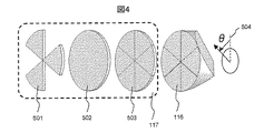
コーナーキューブプリズム116の偏光補償について詳細に説明する。コーナーキューブプリズム116は図4(a)に示すように、ガラスなどの媒質を切り出して立方体の3面を構成したものである。コーナーキューブプリズム116への入射光は、この3面によって反射され、入射光と正反対の方向に戻り光として出射される。ここで、各反射面での反射は全反射条件を満たすため、所定の入射角に応じた位相差が、入射面に対するp偏光とs偏光の間に発生する。このため戻り光は偏光と波面が乱れる。しかも光の入射する位置によって3つの反射面を反射する順番が異なることにより、偏光の乱れ方が異なる。図4(b)はコーナーキューブプリズム116を入射光の方向から見たときの図であり、ここに示す(1)(2)(3)(4)(5)(6)の領域においてそれぞれ異なる偏光擾乱が発生する。但し図の太線は反射面どうしの境界線を表している。これを補正するには、図5のように3分割位相板501と、λ/4板502と、6分割λ/2板503からなる偏光補償素子117を挿入すればよい。λ/4板,6分割λ/2板は偏光の補償だけでなく,入射光に対して戻り光の偏光を90度回転させる機能も兼ねている。また,3分割位相板は特定領域の水平偏光と垂直偏光の間に所定の位相差 φp-φs (φp,φsはそれぞれ水平偏光,垂直偏光に発生する位相)を発生させるもので,入射時に本素子を通過する領域と通過しない領域の間の位相差を補償し、戻り光の波面をそろえる役割を持つ。例として、光の波長が405nm、コーナーキューブプリズム116の媒質がBK7であるときの3分割位相板、λ/4板と、6分割λ/2板の設定値を表1に示す。角度の定義は図4に示すように、垂直偏光方向405を0度とし、入射光方向から見て反時計回りを正としている。

次に、光の干渉によって増幅信号と位相誤差信号を得る過程を詳細に説明する。まず、光学系が理想的な状態にある場合を考える。集光レンズ113に入射する光は、水平偏光であるコーナーキューブプリズム116からの戻り光と、垂直偏光である光ディスク109からの戻り光が同軸になったものである。従って光の偏光状態をジョーンズベクトルで表すと
Next, a process for obtaining an amplified signal and a phase error signal by light interference will be described in detail. First, consider a case where the optical system is in an ideal state. The light incident on the
となる。ここでEsは信号光の電場、Erは参照光の電場である。また、このベクトルの第一成分は水平偏光を、第二成分は垂直偏光を表す。この光は無偏光ビームスプリッタ118によって透過光、反射光に2分割され、透過光は軸方向が水平偏光方向から見て22.5度の方向にfast軸を持つλ/2板119を通過する。このときジョーンズベクトルは
It becomes. Here, Es is an electric field of signal light, and Er is an electric field of reference light. The first component of the vector represents horizontal polarization, and the second component represents vertical polarization. This light is divided into two by transmitted light and reflected light by the
となる。次に偏光ビームスプリッタ120によって水平偏光成分が透過し、垂直偏光成分が反射するため、透過する光と反射する光の電場はそれぞれ
It becomes. Next, since the horizontal polarization component is transmitted by the
となる。一方、無偏光ビームスプリッタ118を反射した光は、軸方向が水平偏光方向から見て45度の方向にfast軸を持つλ/4板123を通過する。このときジョーンズベクトルは
It becomes. On the other hand, the light reflected by the
となる。次に偏光ビームスプリッタ124によって水平偏光成分が透過し、垂直偏光成分が反射するため、透過する光と反射する光の電場はそれぞれ
It becomes. Next, since the horizontal polarization component is transmitted by the
となる。従って4つの検出器121,122,125,126の検出信号はそれぞれ、
It becomes. Therefore, the detection signals of the four
となる。ηは検出器の変換効率である。Δφは信号光の位相と参照光の位相の差、すなわち干渉位相である。これらをそれぞれA1,A2,A3,A4とおくと、差動信号D1,D2はそれぞれ It becomes. η is the conversion efficiency of the detector. Δφ is the difference between the phase of the signal light and the phase of the reference light, that is, the interference phase. If these are A1, A2, A3, A4 respectively, the differential signals D1, D2 are respectively
と表される。出力D1はΔφ=0のとき、 It is expressed. When output D1 is Δφ = 0,
となり、信号光の電場Esが参照光の電場Erによって増幅された形をしている。したがって光ディスクの反射率が低い等の理由によってEsが小さく、直接信号光を検出しても正しく信号が再生できない場合であっても、信号を増幅して正しく再生することが可能になる。 Thus, the electric field Es of the signal light is amplified by the electric field Er of the reference light. Therefore, even if the Es is small due to the low reflectivity of the optical disk and the signal cannot be reproduced correctly even if the signal light is detected directly, the signal can be amplified and reproduced correctly.
一方、干渉位相Δφは時間とともに変動する。干渉位相Δφは光路長差ΔL、光源の波長λとの間に On the other hand, the interference phase Δφ varies with time. The interference phase Δφ is between the optical path length difference ΔL and the wavelength λ of the light source.
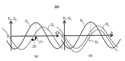
の関係がある。干渉位相を一定に保つには光路長差を光源の波長より十分小さな精度、すなわち10ナノメートル程度以内に抑える必要がある。前述のように光路長差はアクチュエータ107と可動部114によりゼロになるように調整されるが、通常の焦点ずれ信号によるアクチュエータの制御においては、残差として焦点位置に数10ナノメートルの誤差が残る(通常の再生信号を取得する場合は問題ない)だけでなく、制御時のアクチュエータのわずかな傾きにより余分な光路長差が発生したり、光ディスクのカバー層の厚み誤差による光路長差誤差が発生したりするため、通常は数μm程度の誤差が残ってしまう。ここで出力D2を、本誤差をキャンセルするために利用する。光路長差に対するD1,D2の変化を図5に示す。D1(RF信号)が最大となるΔL=0においてD2はゼロとなり、ちょうどフォーカス誤差信号やトラック誤差信号のようなS字カーブの形になっている。従って本信号を位相誤差信号とし、常にゼロになるように閉ループ制御(以後、位相サーボと呼ぶ)することにより干渉位相の制御が可能となる。本実施例では本誤差信号をピエゾ素子の駆動電圧129にフィードバックしてミラー130を前後方向に動かすことによって光路長(干渉位相)の制御を行っている。この場合、例えば光路長差が正の値にずれた時、ピエゾ素子の駆動電圧が増加し、ミラーが前に押し出されて信号光の光路長が短くなり、光路長差が負の方向に向かう。光路長差が負の方向に動いた場合は逆に光路長差が正の方向に向かう。このようにして干渉位相をゼロに保つことができ、安定な増幅信号を得ることができる。
There is a relationship. In order to keep the interference phase constant, it is necessary to suppress the optical path length difference to an accuracy sufficiently smaller than the wavelength of the light source, that is, within about 10 nanometers. As described above, the optical path length difference is adjusted to be zero by the
次に、干渉信号出力が不完全な場合について説明する。実際の光ヘッドにおいては、光ヘッド組み立て誤差や部品の加工精度などに起因して、光学系の各種パラメータ、例えばハーフビームスプリッタ118の反射率、透過率、遅延量や、λ/2板119,λ/4板123の遅延量、設定角、あるいは検出器121,122,125,126の変換効率、オフセットなどには、理想的な値からの誤差が重畳する。これらの誤差がある場合、D1,D2は一般に
Next, a case where the interference signal output is incomplete will be described. In an actual optical head, various parameters of the optical system, such as reflectivity, transmittance, delay amount of the
の形で表される。ここで、 aが差動信号D1における信号増幅率、r,b1,b2,δは、光ヘッド光学系自身の持つ特性誤差量を示す定数であり、rが差動信号D1と差動信号D2とに含まれるそれぞれの変動成分の最大振幅の比、b1が差動信号D1に含まれる直流信号成分、b2が差動信号D2に含まれる直流信号成分、δが差動信号D1とD2の位相差である。 It is expressed in the form of Here, a is the signal amplification factor in the differential signal D1, r, b1, b2, and δ are constants indicating the characteristic error amount of the optical head optical system itself, and r is the differential signal D1 and the differential signal D2. Ratio of the maximum amplitude of each fluctuation component included in 1 and 2, b1 is a DC signal component included in the differential signal D1, b2 is a DC signal component included in the differential signal D2, and δ is the order of the differential signals D1 and D2. It is a phase difference.
上記の誤差量を含んだ光ヘッドの差動信号出力D1,D2は、図6(a)のように表される。ここで、図中の(1)はオフセット誤差(b2)、(2)は位相誤差(δ)を表す。これらの誤差が存在する場合、D1が最大値を取る位相において、D2がゼロでない値を取るため、このまま位相サーボを駆動すると適切な位相にロックされず、再生信号の増幅率が低下してしまう。このような場合は、図6(b)の白矢印で表されるように、D2にオフセットを与えることにより、位相差ゼロの位置でD2がゼロになるようにすればよい。なお、D1にもオフセットやゲインの誤差が生じるが、従来と同等の信号処理系で十分取り除くことが可能である。
なお、本方式の出力(式14)の二乗を再生信号として扱っても良い。これにより、DVDやブルーレイディスクのような従来の光ディスク信号と同じく、信号光強度に比例した再生信号出力となるため、従来の信号処理系を用いることができる。
The differential signal outputs D1 and D2 of the optical head including the above error amount are expressed as shown in FIG. Here, (1) in the figure represents the offset error (b2), and (2) represents the phase error (δ). If these errors exist, D2 takes a non-zero value in the phase where D1 takes the maximum value, so if the phase servo is driven as it is, it will not be locked to an appropriate phase, and the amplification factor of the reproduction signal will decrease . In such a case, as indicated by the white arrow in FIG. 6B, an offset is given to D2, so that D2 becomes zero at the position where the phase difference is zero. Note that offset and gain errors also occur in D1, but can be sufficiently removed by a signal processing system equivalent to the conventional one.
Note that the square of the output of this method (Equation 14) may be treated as a reproduction signal. As a result, the reproduction signal output is proportional to the signal light intensity, as in the case of conventional optical disc signals such as DVD and Blu-ray disc, so that a conventional signal processing system can be used.
図1に示した光ヘッドと同等の機能は他の構成でも実現可能であり、原理的には3つ以上の検出器で、各検出器上での信号光と参照光の位相差が互いに異なるように検出を行えばよい。例として、図7に、光ヘッドの検出光学系を3つの検出器を用いて構成した場合の光ディスク装置の構成例を示す。なお、図7において、信号処理回路やプロセッサなど、他の構成要素は図1に示す光ディスク装置の構成と同一であるものとする。図7に示す光学系では、信号光と参照光の位相差が各検出器上でそれぞれ0度、120度、240度となる。集光レンズ113を通過した光は、無偏光ビームスプリッタ701、702によって3つの光束に分割され、それぞれ45度偏光を透過する偏光子703、704、705を通過したのちに検出器706、707、708によって検出される。この3つの光束のうち、ひとつには信号光と参照光の間に第1の位相差を発生させる位相板709が、もうひとつには信号光と参照光との間に第2の位相差を発生させる位相板710がそれぞれ挿入されている。なお、本実施例では、第1の位相差を60度、第2の位相差を−60度となるように位相板を設定した。
なお、ここで位相差とは、位相板において発生する水平偏光成分の位相に対する、垂直偏光成分の位相の符号付き大きさである。また、各検出器上での光量が等しくなるように、無偏光ビームスプリッタ701は透過率と反射率の比が1対2に、無偏光ビームスプリッタ702は透過率と反射率が等しくなるようなものを使用する。
Functions equivalent to those of the optical head shown in FIG. 1 can be realized by other configurations. In principle, the phase difference between the signal light and the reference light on each detector is different between three or more detectors. Detection may be performed as follows. As an example, FIG. 7 shows an example of the configuration of an optical disc apparatus when the detection optical system of the optical head is configured using three detectors. In FIG. 7, other components such as a signal processing circuit and a processor are the same as those of the optical disc apparatus shown in FIG. In the optical system shown in FIG. 7, the phase difference between the signal light and the reference light is 0 degrees, 120 degrees, and 240 degrees on each detector, respectively. The light that has passed through the
Here, the phase difference is a signed magnitude of the phase of the vertical polarization component with respect to the phase of the horizontal polarization component generated in the phase plate. Further, the
以上をまとめると、検出器708には、信号光と参照光とで位相差の無い干渉光が、検出器706には、第1の位相差を持った干渉光が、検出器710には、第2の位相差を持った干渉光がそれぞれ入力される。このとき、位相差の無い干渉光の光の強度をI1、第1の位相差を持った干渉光の強度をI2、第2の位相差を持った干渉光の強度をI3とすると、I1,I2,I3は次式のように表せる。
In summary, the
次に、これらの出力信号を演算回路711に入力し、以下の出力D1,D2を生成する。
Next, these output signals are input to the
式21で表される差動信号は、第1の位相差を有する干渉光と第2の位相差を有する干渉光強度出力の平均値から位相差180度の干渉光強度出力を引いた信号であり、式22で表される差動信号は、第1の位相差を有する干渉光強度出力と第2の位相差を有する干渉光強度出力との差分信号に√3/2を乗算したものである。 The differential signal represented by Equation 21 is a signal obtained by subtracting the interference light intensity output with a phase difference of 180 degrees from the average value of the interference light having the first phase difference and the interference light intensity output having the second phase difference. Yes, the differential signal represented by Equation 22 is obtained by multiplying the difference signal between the interference light intensity output having the first phase difference and the interference light intensity output having the second phase difference by √3 / 2. is there.
これらは図1に示す4つの検出器の例における差動信号D1,D2と同じ形をしている。従って上記のようにD1を再生信号、D2を位相誤差信号として用いることで同様の効果を得ることができる。このように、より少ない検出器点数でも同様の効果を得ることができる。実際の光学系で検出される差動信号には、光ヘッドの組み立て誤差などに起因する誤差が重畳するため、図6で説明したようなオフセット処理などを施して、信号処理を行えばよい。 These have the same shape as the differential signals D1, D2 in the example of the four detectors shown in FIG. Therefore, the same effect can be obtained by using D1 as a reproduction signal and D2 as a phase error signal as described above. Thus, the same effect can be obtained even with a smaller number of detector points. Since an error caused by an optical head assembly error or the like is superimposed on the differential signal detected by the actual optical system, the signal processing may be performed by performing the offset processing described with reference to FIG.
図8には、干渉光学系と検出光学系の更に別の構成例を示す。図8においても、光ヘッド以外の構成要素は図1に示す光ディスク装置の構成と同一であり、従って説明は省略する。図8に示す光ヘッド光学系の干渉光学系では、参照光反射手段として、コーナーキューブプリズム116と偏光補償素子117の代わりに、ミラー801と当該ミラーに入射光束を集光する集光レンズ802が搭載されている。このような構成でもコーナーキューブプリズム116と同様に素子の傾きによる干渉信号振幅の劣化を抑えることができる。また、干渉信号を得るための光学系は、干渉光学素子803と検出器804によって構成されている。干渉光学素子803と検出器804の詳細を図9(a)に示す。干渉光学素子803は、無偏光回折素子901と、異方性媒質902と、ウォラストンプリズム903とからなる。入射する信号光を垂直偏光、参照光を水平偏光とすると、入射光はまず無偏光回折格子901によって0次光と1次光に分割され、それぞれ異方性媒質902に入射する。1次回折光は入射光に対して水平方向に方向を変えて出射される。ここで、異方性媒質の光学軸は、0次光の進行方向を向いているため、1次回折光のみ信号光と参照光との間に遅延が生じ、遅延がπ/2(光路長差λ/4)となるように媒質の厚みが設定されている。その後これらの光束はウォラストンプリズム903に入射し、それぞれ2分割されて検出器904上に配置された4つの受光部により検出される。ウォラストンプリズム903の光線分離方向は、0次光から見て水平方向に対して±45度の方向である。このような構成において、無偏光回折格子901、異方性媒質902、ウォラストンプリズム903はそれぞれ、ハーフビームスプリッタ118、λ/4板123、偏光ビームスプリッタ120と同等の機能を持ち、図1の構成と同じように再生信号と位相誤差信号を得ることが可能である。検出器の詳細は図9(b)に示すとおりである。受光部905,906、907,908は、図1に示す検出器121,122,125,126にそれぞれ対応し、差動回路907,910によりそれぞれ再生信号、位相誤差信号が得られる。差動回路907,910は検出器904に組み込まれており、受光部の検出電流の差分を差動回路によって出力したものをトランスインピーダンスアンプによって電圧信号に変換している。
FIG. 8 shows still another configuration example of the interference optical system and the detection optical system. Also in FIG. 8, the components other than the optical head are the same as those of the optical disk apparatus shown in FIG. In the interference optical system of the optical head optical system shown in FIG. 8, a
光路長差固定位置調整を実行するための光路長差の制御機構は、図1のように干渉光学系の反射光光路上ではなく、参照光光路上に配置しても良い。図10には、光路長差の制御機構として、一対のくさび型プリズム1001,1002を2次元アクチュエータ107上に搭載された収差補正素子117と偏光ビームスプリッタ104との間に配置した構成例を示す。位相誤差信号は、図7,図8に示される構成例と同様に、図示されないサーボ回路79を介して介してくさび型プリズム1001,1002の組にフィードバックされ、位相制御が実行される。図11には、一対のくさび型プリズム1001,1002の相対的な配置関係を示す。片方のプリズム(本実施例ではプリズム1002)はアクチュエータ1003に搭載されており、アクチュエータを光軸方向に動かすことにより光路長の制御が可能である。光路長は、アクチュエータを光軸と垂直方向(紙面に対して左右の方向)に動かしても制御可能である。
例としてくさび型プリズム1001,1002の傾斜角(定義は図11参照)θ=15度、媒質BK7、光源波長λ=405nmとしたとき、位相誤差信号の最大値と最小値の間に対応する光路長差λ/2発生させるのに必要なくさび型プリズムの移動距離は10μmとなる(図12参照)。これは通常の焦点ずれ信号のS字信号の最大値、最小値間の対物レンズの移動量と同程度である。
The optical path length difference control mechanism for executing the optical path length difference fixed position adjustment may be arranged on the reference light optical path instead of the reflected light optical path of the interference optical system as shown in FIG. FIG. 10 shows a configuration example in which a pair of wedge-shaped
As an example, when the inclination angles of the
図13,図14には、光路長差の粗調整機構の別の構成例について示す。図1、図7および図8に示す構成例では、光路長差の粗調整機構として、コーナーキューブプリズム116が対物レンズ108と同一のアクチュエータに搭載されている構成となっていたが、図13のようにこれらが別々のアクチュエータに搭載されていても同様の制御を行うことが可能である。この場合、検出器111で検出された焦点ずれ信号FESが、サーボ回路79を介して、2次元アクチュエータ107とコーナーキューブプリズム116が搭載されているアクチュエータ1301の両方に入力されることにより、光路長差の粗調整が実現できる。図13に示す構成は、図1、図7、図8に示す構成と比較して、アクチュエータ単体への重量負荷が軽減されるため、高速な光路長の調整動作が可能となる。図14には、図13に示す構成において、可動部114やプリズムミラー115を省略した構成を示す。この場合、光路長差固定位置調整はアクチュエータ1301で実行される。この場合、アクチュエータ1301への駆動電流として、焦点ずれ信号にDC成分を加えたものを入力し、DC成分の大きさを変化させることにより光路長差固定位置の調整を行えばよい。
FIG. 13 and FIG. 14 show another configuration example of the optical path length difference coarse adjustment mechanism. In the configuration example shown in FIGS. 1, 7, and 8, the
以上説明した各種の信号処理や制御処理は、信号処理回路25やマイクロプロセッサ27などにより実行される。図20には、信号処理回路25の回路ブロックの構成の具体例を示す。再生信号RFはAD変換回路2101によってデジタル化され、デジタル信号出力Sが得られる。AD変換器のサンプリングのタイミングは、デジタル信号出力Sと電圧制御可変周波数発信器(VCO)2102の出力を位相比較器2103によって位相比較し、位相比較器の出力をローパスフィルタ(LPF)2104によって平均化して、VCOの制御入力へとフィードバックすることによって生成している。すなわち、位相比較器2103、VCO2102、LPF2104によって構成されたPLL(Phase-locked loop)回路によって位相制御されたクロック出力(CK)を得て、AD変換のタイミングを制御している。
デジタル再生信号Sは、適当なデジタル等化処理の後、復調回路24やアドレス検出回路23に入力され、復号回路26によって、ユーザデータとして、メモリ29やマイクロプロセッサ27に送られる。マイクロプロセッサは、上位装置99からの指示によって、サーボ回路79や自動位置制御手段76を制御し、任意のアドレスに光スポット37を位置づける。マイクロプロセッサ27は上位装置からの指示が再生か記録かによって、レーザドライバ28を制御し、レーザ101を適当なパワー/波形で発光させる。また、ビームエキスパンダ1101,可動部114を光軸方向に動かし、信号品質が最も良くなる位置に固定する。サーボ回路79は、焦点ずれ信号、トラックずれ信号に基づき2次元アクチュエータ107を制御し、光ディスク109の記録面に集光され、記録トラックを追従するようにする。また、差動回路128より生成される位相誤差信号に基づきピエゾ素子801を制御し、干渉位相がゼロになるようにする。
The various signal processing and control processing described above are executed by the
The digital reproduction signal S is input to the
図21は可動部やアクチュエータの制御の手順の一例を示したフローチャートである。まず、焦点ずれ信号、トラックずれ信号、光路長差固定位置、球面収差補正量の粗調整を行う(順番は任意)。焦点ずれ信号、トラックずれ信号に関しては電気的なオフセットを除去すればよく、光路長差固定位置、球面収差補正量に関してはディスクの種類や再生する層番号などに応じて特定の値を設定すればよい。次に焦点ずれ信号、トラックずれ信号に基づいてフォーカスサーボ、トラックサーボをこの順に駆動する。次に位相誤差信号の振幅が最大となるよう、可動部114を駆動して光路長差の調整を行う(光路長差固定位置粗調整)。次に位相誤差信号に基づき位相サーボを駆動する。この時点で安定化された再生信号が取得できるため、最後に再生信号品質をモニタしながら、焦点ずれ信号のオフセット、トラックずれ信号のオフセット、光路長差固定位置、球面収差補正量のそれぞれについて、再生信号品質が最も良くなる位置を探索、学習して設定する(FESオフセット微調整、TESオフセット微調整、光路長固定位置微調整、球面収差補正微調整)。
FIG. 21 is a flowchart showing an example of a procedure for controlling the movable part and the actuator. First, coarse adjustment is performed for the defocus signal, the track shift signal, the optical path length difference fixed position, and the spherical aberration correction amount (the order is arbitrary). It is only necessary to remove the electrical offset for the focus error signal and the track error signal, and the optical path length difference fixed position and the spherical aberration correction amount should be set to specific values according to the type of disk, the layer number to be reproduced, and the like. Good. Next, the focus servo and the track servo are driven in this order based on the focus error signal and the track error signal. Next, the optical path length difference is adjusted by driving the
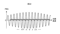
光路長差固定位置微調整の具体的方法の一例を説明する。まず、位相誤差信号に付加するオフセット値を調整することで、干渉信号品質が最も良くなる位置を探索する。次に、以下に説明するような位相ジャンプを行う。光路長差が変化したときの位相誤差信号は図22のようになる。図の黒丸が位相ゼロの位置であり、位相サーボ駆動時はこのうちのいずれかに固定される。このとき、隣接する黒丸の位置には、光路長差を位置誤差信号PESの周期に対応する量だけ変化させる(以下、位相ジャンプと呼ぶ)ことにより移動させることができる。制御上は、光路長差の微調整手段(例えば、図1のミラー130とピエゾ素子129)に対して、位相ジャンプを発生させるための位相ジャンプ信号を供給することにより実現される。位相ジャンプ信号は目標位置に移動させるための移動パルスと、目標位置付近で移動を止める制動パルスからなり、サーボ信号回路により生成される。従って、位相ジャンプによって任意の位相ゼロの位置に移動することができるため、再生信号品質が最も良くなる場所を探索、学習して設定すればよい。
An example of a specific method for fine adjustment of the optical path length difference fixed position will be described. First, the position where the interference signal quality is the best is searched by adjusting the offset value added to the phase error signal. Next, a phase jump as described below is performed. The phase error signal when the optical path length difference changes is as shown in FIG. The black circle in the figure is the position of phase zero, and is fixed to one of these during phase servo driving. At this time, the position of the adjacent black circle can be moved by changing the optical path length difference by an amount corresponding to the period of the position error signal PES (hereinafter referred to as phase jump). The control is realized by supplying a phase jump signal for generating a phase jump to a means for finely adjusting the optical path length difference (for example, the
このような探索動作あるいは学習動作は、メモリ28、マイクロプロセッサ27およびサーボ回路79により実行される。サーボ回路79は、光路長固定位置調整手段ないし光路長差微調整手段に対し位相ジャンプ信号を供給し、光路長固定位置調整手段ないし光路長差微調整手段は位相ジャンプ信号に従って光ヘッド光学系の光路長を所定量だけ変化させる。ここで、位相ジャンプ信号は光路長差がおよそ光源の波長程度ジャンプするように予め位相サーボ回路79に設定されている。このため位相ジャンプが終了した直後に再び位相サーボが駆動され、光路長差はちょうど1波長分ずれた位置に固定される。なお、位相ジャンプは1波長分とは限らず、2波長分など、波長の整数倍だけジャンプするような位相ジャンプ信号を用いてもよい。
Such search operation or learning operation is executed by the memory 28, the
本実施例はDVDやブルーレイディスクのような、通常の光ディスクの再生を前提としているが、入射光と変調された信号光がコヒーレントで同一の波長であれば、特に形態は問わない。例えばホログラムメモリや、近接場メモリなどの大容量メモリにおいても本発明は適用可能である。 The present embodiment is premised on reproduction of a normal optical disc such as a DVD or a Blu-ray disc, but the form is not particularly limited as long as the incident light and the modulated signal light are coherent and have the same wavelength. For example, the present invention can be applied to a large capacity memory such as a hologram memory or a near field memory.
以上、本実施例の光ディスク装置により、光ピックアップ光学系の持つ光路長の揺らぎを調整する機能を備えた光ディスク装置およびその機能を実現するために必要な機構を備え、このために安定した増幅信号を得ることが可能な光ピックアップが実現される。 As described above, the optical disk apparatus according to the present embodiment includes the optical disk apparatus having the function of adjusting the fluctuation of the optical path length of the optical pickup optical system and the mechanism necessary for realizing the function, and a stable amplified signal for this purpose. An optical pickup capable of obtaining the above is realized.
図15には、光路長差固定位置調整と位相サーボを同一の可動部によって行う形態の光ディスク装置の構成例を示す。図15では、光ディスクの構成要素のうち、光ヘッドの光学系およびアクチュエータ、光ディスクおよび光ディスク支持機構のみを示し、図1と共通な構成要素については図示を省略している。しかし実際には、再生信号処理ブロック2やマイクロプロセッサ27、あるいはサーボ回路79など、図1と同様な構成例を含んでいる。図15に示す光ディスク装置では、図1に示されるプリズムミラー115をアクチュエータ1501に搭載し、アクチュエータ1501の駆動電流として、位相誤差信号にマイクロプロセッサ27からサーボ回路79へ指示された所定のDC成分を付加したものを入力する。ここでDC成分の値を調整することにより光路長差固定位置の調整を行い、位相誤差信号成分を用いて位相サーボを駆動する。DC成分の大きさは、アクチュエータ1501の移動量が実施例1の可動部114に与えられる移動量と同様に、多層光ディスクの異なる層や光ディスクの種類などに応じて所定の値に決定さる。すなわち、DC成分の値を調整することが、実施例1における可動部114の移動量調整と同じく、光路長差固定位置を調整する役割を担っている。
FIG. 15 shows a configuration example of an optical disc apparatus in which the optical path length difference fixed position adjustment and the phase servo are performed by the same movable part. FIG. 15 shows only the optical system and actuator of the optical head, the optical disc, and the optical disc support mechanism among the components of the optical disc, and the components common to FIG. 1 are not shown. However, actually, the reproduction
このような構成とすることで、部品点数を削減し、光学系を小型に構成することが可能である。 With such a configuration, the number of parts can be reduced and the optical system can be made compact.
図16には、3次元アクチュエータ1601によって位相サーボを行う機能を備えた光ディスク装置の構成例を示す。図16も、図15同様、図1と共通な構成要素については図示を省略しているが、実際の制御動作を実行するための構成要素を含む。3次元アクチュエータ1601とは、通常の2次元アクチュエータに加え、光軸方向の傾きの制御が可能なアクチュエータである。この光軸方向の傾きにより、信号光と参照光の光路長差が変化する為、位相誤差信号PESを光軸方向の傾きにフィードバックして位相サーボを駆動する。なお、位相誤差信号PESを生成するための光学系の構成・機能などは、図1と同様であるので説明は省略する。
FIG. 16 shows a configuration example of an optical disc apparatus having a function of performing phase servo by a three-
このような構成とすることで実施例2と同様に、光路長差調整に必要な部品点数の削減を行うことができ、光学系を小型に構成することが可能である。 By adopting such a configuration, similarly to the second embodiment, it is possible to reduce the number of parts necessary for adjusting the optical path length difference, and it is possible to make the optical system compact.
図17には、光路長差の粗調整、固定位置調整、微調整を同一の素子で行う機能を備えた光ディスク装置の構成例を示す。図17も、図15および図16と同様、図1と共通な構成要素については図示を省略している。図17に示す光ディスク装置では、対物レンズ108やコーナーキューブプリズム116を搭載するアクチュエータが3次元アクチュエータ1601により構成されており、XYZ方向への駆動の他、搭載される光学素子を光軸に対して傾けるように可動できる。光路長の粗調整動作は3次元アクチュエータ1601のZ方向への移動により実行され、固定位置調整および微調整動作は、X方向あるいはY方向を回転軸とする回転動作により、対物レンズ108やコーナーキューブプリズム116の光軸に対する傾きを変えて実行される。3次元アクチュエータ1601は、サーボ回路79で制御される。光軸方向の傾きを調整するための制御信号としては、光路長差固定位置の調整のためのDC電流をオフセットとして加えられた位相誤差信号電流が入力される。
FIG. 17 shows a configuration example of an optical disc apparatus having a function of performing coarse adjustment, fixed position adjustment, and fine adjustment of the optical path length difference with the same element. In FIG. 17, as in FIGS. 15 and 16, the components common to FIG. 1 are not shown. In the optical disk apparatus shown in FIG. 17, the actuator on which the
このような構成とすることで実施例2、実施例3と同様に、光路長差調整に必要な部品点数の削減を行うことができ、光学系を小型に構成することが可能である。 By adopting such a configuration, it is possible to reduce the number of parts necessary for adjusting the optical path length difference and to make the optical system compact as in the second and third embodiments.
本実施例は、実施例1の光ディスク装置の無偏光ビームスプリッタ118の反射率および透過率が異なる場合の構成例である。実施例1における無偏光ビームスプリッタ118は一般的な、反射率と透過率が等しいもの(ハーフビームスプリッタ)であった。差動信号D1には再生信号成分が含まれるため、検出器121、122は再生信号を取得するのに十分な帯域が必要である。一方差動信号D2は再生信号成分がカットされている必要があるため、検出器124,125は検出器121、122に比べて要求される帯域が狭い。一般に、検出器のアンプゲインとカットオフ周波数はトレードオフの関係にあるため、検出器124,125は相対的に検出器のアンプゲインを高く設定することができ、その結果必要とされる光信号の大きさは相対的に小さくなる。すなわち、無偏光ビームスプリッタ118の透過率を反射率よりも大きく設定することにより、再生信号の振幅を大きくすることができる。たとえばブルーレイディスクを4倍速で再生すると仮定した場合、再生信号には100MHz、位相誤差信号には200kHz程度の帯域が必要であるため、無偏光ビームスプリッタの反射率は透過率の1%程度に設定すれば十分である。
This embodiment is a configuration example in the case where the reflectance and transmittance of the
本構成により、信号増幅効果をより大きくすることができ、光ディスク装置の性能を一段と向上させることが可能となる。 With this configuration, the signal amplification effect can be further increased, and the performance of the optical disc apparatus can be further improved.
本実施例では、位相誤差信号のゲインを自動調整する機能を備えた光ディスク装置について説明する。図18には、本実施例の機能を有する光ディスク装置の構成例を示す。位相誤差信号は、検出信号から再生信号成分を落としたものであるため、光源の発光パワーが一定であっても、記録部か未記録部か、あるいは変調の深さなどによって振幅が変動する。このため本実施例では信号光の一部を、信号光を生成するための光路上に配置された特殊偏光ビームスプリッタ1801(特殊偏光ビームスプリッタ105と同等のもの)で反射させることによって取り出し、集光レンズ1802を用いて検出器1803に導き、平均パワー信号Gを出力する。出力された平均パワー信号Gは、差動検出器128の後段に配置された除算回路1804に入力される。実施例1で説明したように、差動検出器128の出力D2は位相誤差信号に相当する。当該除算回路1804により、位相誤差信号を平均パワー信号で除算(規格化)する演算処理が実行される。これにより、光ディスクの状態によらない一定振幅の位相誤差信号を得ることができ、安定な位相サーボ駆動が可能となる。
In this embodiment, an optical disk apparatus having a function of automatically adjusting the gain of a phase error signal will be described. FIG. 18 shows a configuration example of an optical disc apparatus having the functions of this embodiment. Since the phase error signal is obtained by removing the reproduction signal component from the detection signal, even if the light emission power of the light source is constant, the amplitude varies depending on whether it is a recorded portion or an unrecorded portion, or the depth of modulation. For this reason, in this embodiment, a part of the signal light is extracted by being reflected by a special polarization beam splitter 1801 (equivalent to the special polarization beam splitter 105) disposed on the optical path for generating the signal light, and collected. An
図18では、平均パワー信号Gを取得するための光学的な分岐と検出器を新たに設けた構成例について説明したが、図19のように検出器111の出力信号を用いて取得してもよい。この場合、図2に示される受光部201,202,203,204の出力の総和A+B+C+D(但し、帯域制限により再生信号成分を落としたもの)が平均パワー信号Gとなる。従って、図19では、図2の構成に加えて、受光部201,202,203,204の出力の総和A+B+C+Dを算出するための論理回路素子を備えた四分割検出器が、平均パワー信号Gの取得手段として搭載される。
In FIG. 18, the configuration example in which the optical branch and the detector for obtaining the average power signal G are newly provided has been described. However, even if the output is obtained using the output signal of the
以上、本実施例の構成により、実施例1から5に示す構成と比較して、安定な位相サーボ駆動が可能な光ディスク装置および光ヘッドが実現できる。
As described above, with the configuration of this embodiment, an optical disc apparatus and an optical head capable of stable phase servo drive can be realized as compared with the configurations shown in
本実施例は、実施例1において、光路長差固定位置微調整を、ピエゾ素子129と可動部114との組み合わせにより本調整を行う場合である。具体的には、図23のように位相ジャンプの繰り返しによりピエゾ素子のストローク範囲の端付近まで到達したときに、可動部を移動させる。すると、閉ループ制御を行っているために光路長差の変化を伴わずにピエゾ素子が(可動部と連動して)伸縮するため、更に位相ジャンプを行うことが可能となり、原理的には可動部のストローク範囲内で位相ジャンプを繰り返すことが可能となる。すなわち、ピエゾ素子129のストロークが短い場合でも十分な光路長差調整範囲を確保することができる。
The present embodiment is a case where the fine adjustment of the optical path length difference fixed position is performed by the combination of the
ピエゾ素子は応答速度を十分に確保するため、伸縮方向の長さは短いほうが望ましいが、伸縮方向の長さはピエゾ素子のストロークに比例するため、応答速度とストロークがトレードオフの関係にある。従って本構成により、短いストロークを許容することでピエゾ素子の応答速度を確保し、当該光ディスク装置の再生速度の高速化に寄与することができる。また、ピエゾ素子を小型化する効果も有するため、光ディスク装置、特に光ヘッド部の小型化に寄与することができる。 The piezoelectric element preferably has a short length in the expansion / contraction direction in order to secure a sufficient response speed. However, since the length in the expansion / contraction direction is proportional to the stroke of the piezo element, the response speed and the stroke are in a trade-off relationship. Therefore, with this configuration, it is possible to secure a response speed of the piezo element by allowing a short stroke, and to contribute to an increase in the reproduction speed of the optical disc apparatus. Moreover, since it has the effect of reducing the size of the piezo element, it can contribute to the downsizing of the optical disk device, particularly the optical head unit.
本発明により、大容量多層高速光ディスクの再生信号が安定に、高品質で検出することが可能となり、大容量ビデオレコーダや、ハードディスクデータバックアップ装置、保存情報アーカイブ装置など、幅広い産業応用が期待できる。 According to the present invention, it becomes possible to detect a reproduction signal of a large-capacity multilayer high-speed optical disk stably and with high quality, and a wide range of industrial applications such as a large-capacity video recorder, a hard disk data backup device, and a stored information archive device can be expected.
2:再生信号処理ブロック、23:アドレス検出回路、24:復調回路、25:信号処理回路、26:復号回路、27:マイクロプロセッサ、28:レーザドライバ、29:メモリ、79:サーボ回路、76:自動位置制御手段、77:モータ、37:光スポット、99:上位装置、2001:光ヘッド、101:半導体レーザ、102:コリメートレンズ、103:λ/2板、104:偏光プリズム、105:特殊偏光ビームスプリッタ、106:λ/4板、107:2次元アクチュエータ、108:対物レンズ、109:光ディスク、110:集光レンズ、111:検出器、112:演算回路、113:集光レンズ、114:可動部、115:プリズムミラー、116:コーナーキューブプリズム、117:偏光補償素子、118:無偏光ハーフビームスプリッタ、119:λ/2板、120:偏光ビームスプリッタ、121、122:検出器、123:λ/4板、124:偏光ビームスプリッタ、125、126:検出器、127、128:差動回路、129:ピエゾ素子,130:ミラー、201,202,203,204:受光部、205:入射ビーム、501:3分割位相板、502:λ/4板、503:6分割波長板、504:垂直偏光方向、701、702:無偏光ビームスプリッタ、703,704,705:偏光子、706,707,708:検出器、709,710:位相板、711:演算回路、801:ミラー、802:集光レンズ、803:干渉素子、804:検出器、901:無偏光回折格子、902:異方性媒質、903:ウォラストンプリズム、905,906,908,909:受光部、907,910:差動回路1001,1002:くさび型プリズム,1003:アクチュエータ1301:アクチュエータ、1601:アクチュエータ、1801:特殊偏光ビームスプリッタ、1802:集光レンズ、1803:検出器、1804:除算回路2101:AD変換回路、2102:電圧制御発信機、2103:位相比較器、2104:ローパスフィルタ 2: Reproduction signal processing block, 23: Address detection circuit, 24: Demodulation circuit, 25: Signal processing circuit, 26: Decoding circuit, 27: Microprocessor, 28: Laser driver, 29: Memory, 79: Servo circuit, 76: Automatic position control means, 77: motor, 37: light spot, 99: host device, 2001: optical head, 101: semiconductor laser, 102: collimating lens, 103: λ / 2 plate, 104: polarizing prism, 105: special polarization Beam splitter, 106: λ / 4 plate, 107: two-dimensional actuator, 108: objective lens, 109: optical disk, 110: condenser lens, 111: detector, 112: arithmetic circuit, 113: condenser lens, 114: movable Part, 115: prism mirror, 116: corner cube prism, 117: polarization compensation element, 118: non-polarization half beam splitter, 119: λ / 2 plate, 120: polarization beam splitter, 121, 122: detector, 123: λ / 4 plate, 124: polarized beam split 125, 126: detector, 127, 128: differential circuit, 129: piezo element, 130: mirror, 201, 202, 203, 204: light receiving unit, 205: incident beam, 501: three-divided phase plate, 502: λ / 4 plate, 503: 6-divided wave plate, 504: Vertical polarization direction, 701, 702: Non-polarization beam splitter, 703, 704, 705: Polarizer, 706, 707, 708: Detector, 709, 710: Phase plate, 711: Arithmetic circuit, 801: Mirror, 802: Condensing Lens, 803: Interference element, 804: Detector, 901: Non-polarized diffraction grating, 902: Anisotropic medium, 903: Wollaston prism, 905,906,908,909: Light receiving unit, 907,910: Differential circuit 1001, 1002: Wedge prism, 1003: Actuator 1301: Actuator, 1601: Actuator, 1801: Special polarization beam splitter, 1802: Condensing lens, 1803: Detector, 1804: Divider circuit 2101: AD converter circuit, 2102: Voltage control transmitter, 2103: Phase comparison , 2104: Low-pass filter
Claims (13)
当該分割された光束の一方を光情報記録媒体に照射することにより得られる信号光と前記分割された光束の他方から得られる参照光とを光学的に干渉させることにより干渉光を形成し、
当該干渉光を複数の検出器に光学的な位相関係が互いに異なる状態で導き、
前記複数の検出器の出力から再生信号を取得する光学的情報再生方法であって、
前記光情報記録媒体の位置変動に伴う、前記信号光と前記参照光の光路長差の変動を打ち消す光路長差粗調整と、
前記干渉光を検出する前記複数の検出器の出力から生成した位相誤差信号に基づいて、前記光路長差の微調整を行う光路長差微調整と、
を行うことを特徴とする光学的情報再生方法。 Split the light beam emitted from the light source,
Forming interference light by optically interfering the signal light obtained by irradiating the optical information recording medium with one of the divided light beams and the reference light obtained from the other of the divided light beams,
The interference light is guided to a plurality of detectors in a state where optical phase relationships are different from each other,
An optical information reproduction method for obtaining a reproduction signal from outputs of the plurality of detectors,
Optical path length difference rough adjustment for canceling the fluctuation of the optical path length difference between the signal light and the reference light accompanying the positional fluctuation of the optical information recording medium;
Based on phase error signals generated from the outputs of the plurality of detectors that detect the interference light, optical path length difference fine adjustment for performing fine adjustment of the optical path length difference;
An optical information reproducing method comprising:
前記光路長差微調整においては、
前記位相誤差信号を光路長差変化手段に入力して閉ループ制御することにより実行されることを特徴とする光学的情報再生方法。 The optical information reproducing method according to claim 1,
In the optical path length difference fine adjustment ,
An optical information reproducing method characterized in that it is executed by Type closed-loop controlling the phase error signal to the optical path length difference changing means.
位相ジャンプ信号を前記光路長差変化手段に入力し、前記閉ループ制御を行ったまま、前記光源の発光波長の整数倍だけ光路長差を可変調整することを特徴とする光学的情報再生方法。 An optical information reproducing method comprising: inputting a phase jump signal to the optical path length difference changing means, and variably adjusting the optical path length difference by an integral multiple of the emission wavelength of the light source while performing the closed loop control.
前記光学モジュールが、 The optical module is
前記光情報記録媒体の位置変動に伴う、前記信号光と前記参照光の光路長差の変動を打ち消す、光路長差の粗調整を行う第1の光路長差変化手段と、 First optical path length difference changing means for performing rough adjustment of the optical path length difference, which cancels out the fluctuation of the optical path length difference between the signal light and the reference light accompanying the positional fluctuation of the optical information recording medium;
前記干渉光を検出する前記複数の検出器の出力から生成した位相誤差信号に基づいて、前記光路長差の微調整を行う第2の光路長差変化手段とを備えたことを特徴とする光ヘッド。 Light comprising: second optical path length difference changing means for finely adjusting the optical path length difference based on phase error signals generated from outputs of the plurality of detectors that detect the interference light. head.
前記光路長差の固定位置を調整する第3の光路長差変化手段とを備えたことを特徴とする光ヘッド。 An optical head comprising: third optical path length difference changing means for adjusting a fixed position of the optical path length difference.
前記第3の光路長差変化手段により、前記参照光と信号光の光路長差がゼロになるように前記参照光と信号光との光路長差が調整され、 The third optical path length difference changing means adjusts the optical path length difference between the reference light and the signal light so that the optical path length difference between the reference light and the signal light becomes zero,
前記第2の光路長差変化手段により、前記参照光と信号光の位相差が所定の閾値以下になるように前記光路差が調整されることを特徴とする光ヘッド。 The optical head is characterized in that the optical path difference is adjusted by the second optical path length difference changing means so that a phase difference between the reference light and the signal light is equal to or less than a predetermined threshold value.
前記第2の光路長差変化手段と、前記第3の光路長差変化手段とが同一の可動部により構成されることを特徴とする光ヘッド。 2. The optical head according to claim 1, wherein the second optical path length difference changing means and the third optical path length difference changing means are constituted by the same movable part.
前記第1の光路長差変化手段と、前記第2の光路長差変化手段と、前記第3の光路長差変化手段とが同一の可動部により構成されることを特徴とする光ヘッド。 An optical head characterized in that the first optical path length difference changing means, the second optical path length difference changing means, and the third optical path length difference changing means are constituted by the same movable part.
前記光学モジュールは、 The optical module is
前記第1の光束を前記光情報記録媒体に集光して照射し、当該光情報記録媒体から反射される反射光を受光する対物レンズと、 An objective lens that collects and irradiates the first light flux on the optical information recording medium and receives reflected light reflected from the optical information recording medium;
前記第2の光束の光路中に設けられ、前記第2の光束を参照光として反射させる参照光反射手段とを有し、 A reference light reflecting means provided in the optical path of the second light flux for reflecting the second light flux as reference light,
前記対物レンズと、前記参照光反射手段とが前記可動部に搭載されていることを特徴とする光ヘッド。 An optical head, wherein the objective lens and the reference light reflecting means are mounted on the movable part.
前記複数の検出器の個数は4つであって、 The number of the plurality of detectors is four,
それぞれの検出器に入射される光の干渉位相が互いに90度の整数倍だけ異なり、 The interference phase of light incident on each detector differs from each other by an integral multiple of 90 degrees,
前記再生信号は入射する光の干渉位相が互いに180度異なる2つの検出器の差動信号であり、 The reproduction signal is a differential signal of two detectors in which the interference phase of incident light is 180 degrees different from each other,
前記位相誤差信号は残りの2つの検出器の間の差動信号であることを特徴とする光ヘッド。 2. The optical head according to claim 1, wherein the phase error signal is a differential signal between the remaining two detectors.
前記光学モジュールは、 The optical module is
無偏光光束分割素子と、 A non-polarizing beam splitting element;
1つまたは複数の波長板と、 One or more wave plates;
複数の偏光分離素子とを備えた干渉光学系を有し、 An interference optical system including a plurality of polarization separation elements;
前記無偏光分割素子が光束を分割する比率が1対1でないことを特徴とする光ヘッド。 An optical head characterized in that the non-polarization splitting element splits a light beam at a ratio of not 1: 1.
前記複数の検出器の出力から位置誤差信号を生成するための論理回路素子と、 A logic circuit element for generating a position error signal from the outputs of the plurality of detectors;
前記光情報記録媒体からの戻り光の平均光量をモニタする総光量検出器と、 A total light amount detector for monitoring the average light amount of the return light from the optical information recording medium;
前記総光量検出器の出力値で前記位相誤差信号に対する規格化演算を実行する除算回路とを有することを特徴とする光ヘッド。 An optical head comprising: a division circuit that performs a normalization operation on the phase error signal with an output value of the total light amount detector.
前記総光量検出器は、焦点ずれ信号を生成する検出器であることを特徴とする光ヘッド。 The optical head according to claim 1, wherein the total light amount detector is a detector that generates a defocus signal.
Priority Applications (2)
| Application Number | Priority Date | Filing Date | Title |
|---|---|---|---|
| JP2009060420A JP5452040B2 (en) | 2009-03-13 | 2009-03-13 | Optical information reproducing method, optical head, and optical disc apparatus |
| PCT/JP2010/053387 WO2010103962A1 (en) | 2009-03-13 | 2010-03-03 | Optical information reproduction method, optical head, and optical disc apparatus |
Applications Claiming Priority (1)
| Application Number | Priority Date | Filing Date | Title |
|---|---|---|---|
| JP2009060420A JP5452040B2 (en) | 2009-03-13 | 2009-03-13 | Optical information reproducing method, optical head, and optical disc apparatus |
Publications (3)
| Publication Number | Publication Date |
|---|---|
| JP2010218591A JP2010218591A (en) | 2010-09-30 |
| JP2010218591A5 JP2010218591A5 (en) | 2011-10-06 |
| JP5452040B2 true JP5452040B2 (en) | 2014-03-26 |
Family
ID=42728252
Family Applications (1)
| Application Number | Title | Priority Date | Filing Date |
|---|---|---|---|
| JP2009060420A Expired - Fee Related JP5452040B2 (en) | 2009-03-13 | 2009-03-13 | Optical information reproducing method, optical head, and optical disc apparatus |
Country Status (2)
| Country | Link |
|---|---|
| JP (1) | JP5452040B2 (en) |
| WO (1) | WO2010103962A1 (en) |
Families Citing this family (11)
| Publication number | Priority date | Publication date | Assignee | Title |
|---|---|---|---|---|
| JP5309008B2 (en) | 2009-12-15 | 2013-10-09 | 日立コンシューマエレクトロニクス株式会社 | Optical information recording / reproducing apparatus and optical information reproducing apparatus |
| JP5409479B2 (en) | 2010-03-29 | 2014-02-05 | 日立コンシューマエレクトロニクス株式会社 | Optical information reproducing apparatus, optical information recording apparatus, and information recording method |
| JP5358530B2 (en) * | 2010-07-28 | 2013-12-04 | 日立コンシューマエレクトロニクス株式会社 | Optical information recording / reproducing apparatus and reproducing apparatus |
| JP2012069189A (en) * | 2010-09-22 | 2012-04-05 | Sony Corp | Reproducing device, and optical path length servo control method |
| JP2012174290A (en) * | 2011-02-17 | 2012-09-10 | Hitachi Media Electoronics Co Ltd | Optical pickup and optical disk unit |
| JP5758728B2 (en) | 2011-07-26 | 2015-08-05 | 株式会社日立ハイテクノロジーズ | Charged particle beam equipment |
| JP2013033572A (en) * | 2011-08-03 | 2013-02-14 | Sony Corp | Optical pickup device and reproducing device |
| WO2014188532A1 (en) * | 2013-05-22 | 2014-11-27 | 日立コンシューマエレクトロニクス株式会社 | Optical information reproduction device |
| JP6471760B2 (en) * | 2015-01-30 | 2019-02-20 | ソニー株式会社 | Playback apparatus and playback method |
| JP7017985B2 (en) | 2018-06-05 | 2022-02-09 | 株式会社日立製作所 | How to determine the system and processing conditions |
| CN109089113B (en) * | 2018-10-12 | 2019-09-10 | 四川长虹电器股份有限公司 | A kind of method of the automatic carry out reproduction ratio adjustment of flat panel TV |
Family Cites Families (6)
| Publication number | Priority date | Publication date | Assignee | Title |
|---|---|---|---|---|
| JP2007317284A (en) * | 2006-05-25 | 2007-12-06 | Hitachi Ltd | Optical disk device |
| JP4564948B2 (en) * | 2006-09-11 | 2010-10-20 | 株式会社日立製作所 | Optical information detection method, optical head, and optical disc apparatus |
| JP4861948B2 (en) * | 2007-02-23 | 2012-01-25 | 株式会社日立製作所 | Optical head and optical disk apparatus |
| JP2008243273A (en) * | 2007-03-27 | 2008-10-09 | Hitachi Ltd | Optical head and method for reproducing optical information recording medium |
| JP2008269680A (en) * | 2007-04-18 | 2008-11-06 | Hitachi Ltd | Optical head and optical disk device |
| JP5153424B2 (en) * | 2008-04-11 | 2013-02-27 | 株式会社日立製作所 | Optical head and optical disk apparatus |
-
2009
- 2009-03-13 JP JP2009060420A patent/JP5452040B2/en not_active Expired - Fee Related
-
2010
- 2010-03-03 WO PCT/JP2010/053387 patent/WO2010103962A1/en active Application Filing
Also Published As
| Publication number | Publication date |
|---|---|
| JP2010218591A (en) | 2010-09-30 |
| WO2010103962A1 (en) | 2010-09-16 |
Similar Documents
| Publication | Publication Date | Title |
|---|---|---|
| JP5452040B2 (en) | Optical information reproducing method, optical head, and optical disc apparatus | |
| JP5153424B2 (en) | Optical head and optical disk apparatus | |
| JP5081763B2 (en) | Optical information detection method, optical pickup, and optical information recording / reproducing apparatus | |
| JP4861948B2 (en) | Optical head and optical disk apparatus | |
| JP4564948B2 (en) | Optical information detection method, optical head, and optical disc apparatus | |
| JP2008269680A (en) | Optical head and optical disk device | |
| JP2007317284A (en) | Optical disk device | |
| JP5043049B2 (en) | Optical information reproducing method and optical disc apparatus | |
| US7764576B2 (en) | Optical information recording and reproducing apparatus | |
| JP2007193894A (en) | Optical recording/reproducing device, optical pickup, and tracking error signal detection method | |
| JP5417269B2 (en) | Optical information reproduction device | |
| US20080267019A1 (en) | Optical Pickup Apparatus and Optical Disk Drive | |
| JP2008243273A (en) | Optical head and method for reproducing optical information recording medium | |
| US20120008483A1 (en) | Optical head and optical disc apparatus | |
| JP4449819B2 (en) | Optical reproducing method, waveform equalizing method, and optical recording / reproducing apparatus | |
| JP6158339B2 (en) | Hologram reproducing apparatus and hologram reproducing method | |
| JP5780932B2 (en) | Optical information recording / reproducing apparatus, optical information recording apparatus | |
| JP2007323791A (en) | Optical information recording and reproducing apparatus | |
| JP5468033B2 (en) | Optical information reproducing apparatus and optical information recording / reproducing apparatus | |
| US20070297731A1 (en) | Optical pick-up | |
| JP2007250034A (en) | Position adjustment method for optical pickup photodetector | |
| US20110002117A1 (en) | Optical disc drive | |
| JP5778624B2 (en) | Optical information reproducing apparatus and optical information reproducing method | |
| WO2013183439A1 (en) | Optical pickup device | |
| WO2012169286A1 (en) | Optical information recording and reproduction device |
Legal Events
| Date | Code | Title | Description |
|---|---|---|---|
| A521 | Written amendment |
Free format text: JAPANESE INTERMEDIATE CODE: A523 Effective date: 20110818 |
|
| A621 | Written request for application examination |
Free format text: JAPANESE INTERMEDIATE CODE: A621 Effective date: 20110818 |
|
| A711 | Notification of change in applicant |
Free format text: JAPANESE INTERMEDIATE CODE: A712 Effective date: 20130529 |
|
| A131 | Notification of reasons for refusal |
Free format text: JAPANESE INTERMEDIATE CODE: A131 Effective date: 20130924 |
|
| A521 | Written amendment |
Free format text: JAPANESE INTERMEDIATE CODE: A523 Effective date: 20131007 |
|
| TRDD | Decision of grant or rejection written | ||
| A01 | Written decision to grant a patent or to grant a registration (utility model) |
Free format text: JAPANESE INTERMEDIATE CODE: A01 Effective date: 20131203 |
|
| A61 | First payment of annual fees (during grant procedure) |
Free format text: JAPANESE INTERMEDIATE CODE: A61 Effective date: 20131227 |
|
| R150 | Certificate of patent or registration of utility model |
Free format text: JAPANESE INTERMEDIATE CODE: R150 |
|
| LAPS | Cancellation because of no payment of annual fees |