JP5452003B2 - 半導体チップの製造方法および半導体モジュールの製造方法 - Google Patents
半導体チップの製造方法および半導体モジュールの製造方法 Download PDFInfo
- Publication number
- JP5452003B2 JP5452003B2 JP2008243438A JP2008243438A JP5452003B2 JP 5452003 B2 JP5452003 B2 JP 5452003B2 JP 2008243438 A JP2008243438 A JP 2008243438A JP 2008243438 A JP2008243438 A JP 2008243438A JP 5452003 B2 JP5452003 B2 JP 5452003B2
- Authority
- JP
- Japan
- Prior art keywords
- substrate
- semiconductor chip
- semiconductor
- cost
- fom
- Prior art date
- Legal status (The legal status is an assumption and is not a legal conclusion. Google has not performed a legal analysis and makes no representation as to the accuracy of the status listed.)
- Active
Links
Images
Classifications
-
- G—PHYSICS
- G06—COMPUTING OR CALCULATING; COUNTING
- G06Q—INFORMATION AND COMMUNICATION TECHNOLOGY [ICT] SPECIALLY ADAPTED FOR ADMINISTRATIVE, COMMERCIAL, FINANCIAL, MANAGERIAL OR SUPERVISORY PURPOSES; SYSTEMS OR METHODS SPECIALLY ADAPTED FOR ADMINISTRATIVE, COMMERCIAL, FINANCIAL, MANAGERIAL OR SUPERVISORY PURPOSES, NOT OTHERWISE PROVIDED FOR
- G06Q50/00—Information and communication technology [ICT] specially adapted for implementation of business processes of specific business sectors, e.g. utilities or tourism
- G06Q50/04—Manufacturing
-
- G—PHYSICS
- G06—COMPUTING OR CALCULATING; COUNTING
- G06Q—INFORMATION AND COMMUNICATION TECHNOLOGY [ICT] SPECIALLY ADAPTED FOR ADMINISTRATIVE, COMMERCIAL, FINANCIAL, MANAGERIAL OR SUPERVISORY PURPOSES; SYSTEMS OR METHODS SPECIALLY ADAPTED FOR ADMINISTRATIVE, COMMERCIAL, FINANCIAL, MANAGERIAL OR SUPERVISORY PURPOSES, NOT OTHERWISE PROVIDED FOR
- G06Q10/00—Administration; Management
- G06Q10/06—Resources, workflows, human or project management; Enterprise or organisation planning; Enterprise or organisation modelling
-
- H—ELECTRICITY
- H10—SEMICONDUCTOR DEVICES; ELECTRIC SOLID-STATE DEVICES NOT OTHERWISE PROVIDED FOR
- H10D—INORGANIC ELECTRIC SEMICONDUCTOR DEVICES
- H10D62/00—Semiconductor bodies, or regions thereof, of devices having potential barriers
- H10D62/80—Semiconductor bodies, or regions thereof, of devices having potential barriers characterised by the materials
- H10D62/83—Semiconductor bodies, or regions thereof, of devices having potential barriers characterised by the materials being Group IV materials, e.g. B-doped Si or undoped Ge
- H10D62/832—Semiconductor bodies, or regions thereof, of devices having potential barriers characterised by the materials being Group IV materials, e.g. B-doped Si or undoped Ge being Group IV materials comprising two or more elements, e.g. SiGe
- H10D62/8325—Silicon carbide
-
- Y—GENERAL TAGGING OF NEW TECHNOLOGICAL DEVELOPMENTS; GENERAL TAGGING OF CROSS-SECTIONAL TECHNOLOGIES SPANNING OVER SEVERAL SECTIONS OF THE IPC; TECHNICAL SUBJECTS COVERED BY FORMER USPC CROSS-REFERENCE ART COLLECTIONS [XRACs] AND DIGESTS
- Y02—TECHNOLOGIES OR APPLICATIONS FOR MITIGATION OR ADAPTATION AGAINST CLIMATE CHANGE
- Y02P—CLIMATE CHANGE MITIGATION TECHNOLOGIES IN THE PRODUCTION OR PROCESSING OF GOODS
- Y02P90/00—Enabling technologies with a potential contribution to greenhouse gas [GHG] emissions mitigation
- Y02P90/30—Computing systems specially adapted for manufacturing
Landscapes
- Engineering & Computer Science (AREA)
- Business, Economics & Management (AREA)
- Human Resources & Organizations (AREA)
- Economics (AREA)
- Strategic Management (AREA)
- General Physics & Mathematics (AREA)
- Tourism & Hospitality (AREA)
- Entrepreneurship & Innovation (AREA)
- Theoretical Computer Science (AREA)
- Marketing (AREA)
- General Business, Economics & Management (AREA)
- Physics & Mathematics (AREA)
- Operations Research (AREA)
- Quality & Reliability (AREA)
- Game Theory and Decision Science (AREA)
- Development Economics (AREA)
- Educational Administration (AREA)
- Manufacturing & Machinery (AREA)
- Health & Medical Sciences (AREA)
- General Health & Medical Sciences (AREA)
- Primary Health Care (AREA)
- Semiconductor Integrated Circuits (AREA)
- Inverter Devices (AREA)
Description
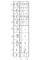
まず、この発明にかかるFOMを式(1)として示す。
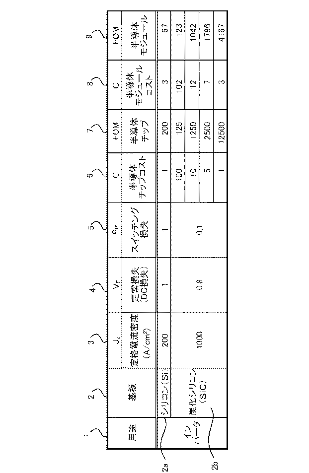
半導体チップのFOM7は、その値が大きい方が有利となる。即ち、半導体チップのFOM7の数値が大きい方が、性能を満足することはもちろんのこと、低コスト化が図られた製品を市場に投入出来ることになるため、市場での競争力向上に繋がり商業的に有利となる。
半導体モジュールのFOM9は、半導体チップのFOM7と同様に、その値が大きい方が有利となる。即ち、半導体モジュールのFOM9の数値が大きい方が、性能を満足することはもちろんのこと、低コスト化が図られた製品を市場に投入出来ることになるため、市場での競争力向上に繋がり商業的に有利となる。
Claims (4)
- 基板の電気的な性能を示す項と半導体チップコストを示す項の積として定められた半導体チップのFOMに基づいて、種類の異なる基板における前記半導体チップのFOMを計算し、その計算結果の大小を比較する比較工程と、
この比較工程による前記計算結果の大小に基づいて、前記種類の異なる基板から所望の基板を選択する選択工程と、
この選択工程により選択された前記所望の基板に半導体素子を形成する素子形成工程とを備え、
前記電気的な性能を示す項は、定格電流密度をJc、定常損失をVF、スイッチング損失をerrとした時に、
Jc/(VF・err)
として表され、
前記半導体チップコストを示す項は、前記半導体チップコストをCとした時に、
1/C
として表され、
前記所望の基板は、前記種類の異なる基板に対する前記FOMの計算結果が大きい方の基板であることを特徴とする半導体チップの製造方法。 - 種類の異なる基板は、シリコン基板および炭化シリコン基板であることを特徴とする請求項1に記載の半導体チップの製造方法。
- 基板の電気的な性能を示す項と半導体モジュールコストを示す項の積として定められた半導体モジュールのFOMに基づいて、種類の異なる基板における前記半導体モジュールのFOMを計算し、その計算結果の大小を比較する比較工程と、
この比較工程による前記計算結果の大小に基づいて、前記種類の異なる基板から所望の基板を選択する選択工程と、
この選択工程により選択された前記所望の基板に半導体素子を形成する素子形成工程と、
この素子形成工程を経て得られた複数の半導体チップを結線しパッケージに収納するパッケージ工程とを備え、
前記電気的な性能を示す項は、定格電流密度をJc、定常損失をVF、スイッチング損失をerrとした時に、
Jc/(VF・err)
として表され、
前記半導体モジュールコストを示す項は、前記半導体モジュールコストをCとした時に、
1/C
として表され、
前記所望の基板は、前記種類の異なる基板に対する前記FOMの計算結果が大きい方の基板である
ことを特徴とする半導体モジュールの製造方法。 - 種類の異なる基板は、シリコン基板および炭化シリコン基板であることを特徴とする請求項3に記載の半導体モジュールの製造方法。
Priority Applications (3)
| Application Number | Priority Date | Filing Date | Title |
|---|---|---|---|
| JP2008243438A JP5452003B2 (ja) | 2008-09-23 | 2008-09-23 | 半導体チップの製造方法および半導体モジュールの製造方法 |
| US12/479,248 US7989227B2 (en) | 2008-09-23 | 2009-06-05 | Method of manufacturing semiconductor chip and semiconductor module |
| DE102009034449.7A DE102009034449B4 (de) | 2008-09-23 | 2009-07-23 | Verfahren zum Herstellen eines Halbleiterchips und eines Halbleitermoduls |
Applications Claiming Priority (1)
| Application Number | Priority Date | Filing Date | Title |
|---|---|---|---|
| JP2008243438A JP5452003B2 (ja) | 2008-09-23 | 2008-09-23 | 半導体チップの製造方法および半導体モジュールの製造方法 |
Publications (2)
| Publication Number | Publication Date |
|---|---|
| JP2010080460A JP2010080460A (ja) | 2010-04-08 |
| JP5452003B2 true JP5452003B2 (ja) | 2014-03-26 |
Family
ID=42038074
Family Applications (1)
| Application Number | Title | Priority Date | Filing Date |
|---|---|---|---|
| JP2008243438A Active JP5452003B2 (ja) | 2008-09-23 | 2008-09-23 | 半導体チップの製造方法および半導体モジュールの製造方法 |
Country Status (3)
| Country | Link |
|---|---|
| US (1) | US7989227B2 (ja) |
| JP (1) | JP5452003B2 (ja) |
| DE (1) | DE102009034449B4 (ja) |
Families Citing this family (2)
| Publication number | Priority date | Publication date | Assignee | Title |
|---|---|---|---|---|
| US9147637B2 (en) * | 2011-12-23 | 2015-09-29 | Infineon Technologies Ag | Module including a discrete device mounted on a DCB substrate |
| US9738195B2 (en) * | 2015-01-23 | 2017-08-22 | David John Willis | Automotive center console armrest storage box lid protector |
Family Cites Families (10)
| Publication number | Priority date | Publication date | Assignee | Title |
|---|---|---|---|---|
| JPH0878439A (ja) * | 1994-09-05 | 1996-03-22 | Mitsubishi Electric Corp | 半導体装置の製造方法 |
| US5493231A (en) * | 1994-10-07 | 1996-02-20 | University Of North Carolina | Method and apparatus for measuring the barrier height distribution in an insulated gate field effect transistor |
| WO1998045719A1 (en) * | 1997-04-04 | 1998-10-15 | University Of Florida | Method for testing and diagnosing mos transistors |
| US7462910B1 (en) | 1998-10-14 | 2008-12-09 | International Rectifier Corporation | P-channel trench MOSFET structure |
| US6621121B2 (en) | 1998-10-26 | 2003-09-16 | Silicon Semiconductor Corporation | Vertical MOSFETs having trench-based gate electrodes within deeper trench-based source electrodes |
| JP4198469B2 (ja) | 2001-04-11 | 2008-12-17 | シリコン・セミコンダクター・コーポレイション | パワーデバイスとその製造方法 |
| GB0327793D0 (en) | 2003-11-29 | 2003-12-31 | Koninkl Philips Electronics Nv | Trench mosfet |
| US7902049B2 (en) * | 2004-01-27 | 2011-03-08 | United Solar Ovonic Llc | Method for depositing high-quality microcrystalline semiconductor materials |
| JP4744958B2 (ja) | 2005-07-13 | 2011-08-10 | 株式会社東芝 | 半導体素子及びその製造方法 |
| JP5017865B2 (ja) | 2006-01-17 | 2012-09-05 | 富士電機株式会社 | 半導体装置 |
-
2008
- 2008-09-23 JP JP2008243438A patent/JP5452003B2/ja active Active
-
2009
- 2009-06-05 US US12/479,248 patent/US7989227B2/en active Active
- 2009-07-23 DE DE102009034449.7A patent/DE102009034449B4/de active Active
Also Published As
| Publication number | Publication date |
|---|---|
| JP2010080460A (ja) | 2010-04-08 |
| US20100075444A1 (en) | 2010-03-25 |
| US7989227B2 (en) | 2011-08-02 |
| DE102009034449A1 (de) | 2010-05-12 |
| DE102009034449B4 (de) | 2016-02-04 |
Similar Documents
| Publication | Publication Date | Title |
|---|---|---|
| Liu | Power electronic packaging: design, assembly process, reliability and modeling | |
| US9721875B2 (en) | Power module and fabrication method for the same | |
| Marcinkowski | Dual-sided cooling of power semiconductor modules | |
| JP2011258623A (ja) | パワー半導体システム | |
| Degrenne et al. | A review of prognostics and health management for power semiconductor modules | |
| CN101853847A (zh) | 组合半导体整流器件和使用该组合半导体整流器件的电功率转换器 | |
| US12500201B2 (en) | Semiconductor element bonding substrate, semiconductor device, and power conversion device | |
| JP6652802B2 (ja) | 半導体装置、および当該半導体装置を備えるインバータ装置 | |
| CN110299350A (zh) | 半导体装置 | |
| US20230207431A1 (en) | Semiconductor device | |
| JPWO2017183580A1 (ja) | 半導体装置、パワーモジュール及びその製造方法 | |
| CN103081327B (zh) | 具有肖特基二极管的整流器装置 | |
| Morroni et al. | Understanding the trade-offs and technologies to increase power density | |
| JP5452003B2 (ja) | 半導体チップの製造方法および半導体モジュールの製造方法 | |
| Liu | Trends of power semiconductor wafer level packaging | |
| Hower et al. | Current status and future trends in silicon power devices | |
| Tang et al. | Degradation in electrothermal characteristics of 4H-SiC junction barrier Schottky diodes under high temperature power cycling stress | |
| Liang et al. | Advanced packaging of SiC power module for automotive applications | |
| Majumdar | Recent technologies and trends of power devices | |
| Siemieniec et al. | Development of low-voltage power MOSFET based on application requirement analysis | |
| US20230207541A1 (en) | Semiconductor device | |
| Narazaki et al. | Direct beam lead bonding for trench MOSFET & CSTBT | |
| JP6269417B2 (ja) | 半導体装置 | |
| Toyoshima et al. | Compact SiC power module for high speed switching | |
| Galiev et al. | Optimization of Liquid Cooling Double-layer Heatsink for SiC Power Modules |
Legal Events
| Date | Code | Title | Description |
|---|---|---|---|
| A621 | Written request for application examination |
Free format text: JAPANESE INTERMEDIATE CODE: A621 Effective date: 20101022 |
|
| A131 | Notification of reasons for refusal |
Free format text: JAPANESE INTERMEDIATE CODE: A131 Effective date: 20130226 |
|
| A977 | Report on retrieval |
Free format text: JAPANESE INTERMEDIATE CODE: A971007 Effective date: 20130228 |
|
| RD01 | Notification of change of attorney |
Free format text: JAPANESE INTERMEDIATE CODE: A7421 Effective date: 20130228 |
|
| A521 | Request for written amendment filed |
Free format text: JAPANESE INTERMEDIATE CODE: A523 Effective date: 20130415 |
|
| TRDD | Decision of grant or rejection written | ||
| A01 | Written decision to grant a patent or to grant a registration (utility model) |
Free format text: JAPANESE INTERMEDIATE CODE: A01 Effective date: 20131203 |
|
| A61 | First payment of annual fees (during grant procedure) |
Free format text: JAPANESE INTERMEDIATE CODE: A61 Effective date: 20131227 |
|
| R150 | Certificate of patent or registration of utility model |
Ref document number: 5452003 Country of ref document: JP Free format text: JAPANESE INTERMEDIATE CODE: R150 Free format text: JAPANESE INTERMEDIATE CODE: R150 |
|
| R250 | Receipt of annual fees |
Free format text: JAPANESE INTERMEDIATE CODE: R250 |
|
| R250 | Receipt of annual fees |
Free format text: JAPANESE INTERMEDIATE CODE: R250 |
|
| R250 | Receipt of annual fees |
Free format text: JAPANESE INTERMEDIATE CODE: R250 |
|
| R250 | Receipt of annual fees |
Free format text: JAPANESE INTERMEDIATE CODE: R250 |
|
| R250 | Receipt of annual fees |
Free format text: JAPANESE INTERMEDIATE CODE: R250 |
|
| R250 | Receipt of annual fees |
Free format text: JAPANESE INTERMEDIATE CODE: R250 |
|
| R250 | Receipt of annual fees |
Free format text: JAPANESE INTERMEDIATE CODE: R250 |
|
| R250 | Receipt of annual fees |
Free format text: JAPANESE INTERMEDIATE CODE: R250 |
|
| R250 | Receipt of annual fees |
Free format text: JAPANESE INTERMEDIATE CODE: R250 |