JP5452003B2 - Semiconductor chip manufacturing method and semiconductor module manufacturing method - Google Patents
Semiconductor chip manufacturing method and semiconductor module manufacturing method Download PDFInfo
- Publication number
- JP5452003B2 JP5452003B2 JP2008243438A JP2008243438A JP5452003B2 JP 5452003 B2 JP5452003 B2 JP 5452003B2 JP 2008243438 A JP2008243438 A JP 2008243438A JP 2008243438 A JP2008243438 A JP 2008243438A JP 5452003 B2 JP5452003 B2 JP 5452003B2
- Authority
- JP
- Japan
- Prior art keywords
- substrate
- semiconductor chip
- semiconductor
- cost
- fom
- Prior art date
- Legal status (The legal status is an assumption and is not a legal conclusion. Google has not performed a legal analysis and makes no representation as to the accuracy of the status listed.)
- Active
Links
Images
Classifications
-
- G—PHYSICS
- G06—COMPUTING OR CALCULATING; COUNTING
- G06Q—INFORMATION AND COMMUNICATION TECHNOLOGY [ICT] SPECIALLY ADAPTED FOR ADMINISTRATIVE, COMMERCIAL, FINANCIAL, MANAGERIAL OR SUPERVISORY PURPOSES; SYSTEMS OR METHODS SPECIALLY ADAPTED FOR ADMINISTRATIVE, COMMERCIAL, FINANCIAL, MANAGERIAL OR SUPERVISORY PURPOSES, NOT OTHERWISE PROVIDED FOR
- G06Q50/00—Information and communication technology [ICT] specially adapted for implementation of business processes of specific business sectors, e.g. utilities or tourism
- G06Q50/04—Manufacturing
-
- G—PHYSICS
- G06—COMPUTING OR CALCULATING; COUNTING
- G06Q—INFORMATION AND COMMUNICATION TECHNOLOGY [ICT] SPECIALLY ADAPTED FOR ADMINISTRATIVE, COMMERCIAL, FINANCIAL, MANAGERIAL OR SUPERVISORY PURPOSES; SYSTEMS OR METHODS SPECIALLY ADAPTED FOR ADMINISTRATIVE, COMMERCIAL, FINANCIAL, MANAGERIAL OR SUPERVISORY PURPOSES, NOT OTHERWISE PROVIDED FOR
- G06Q10/00—Administration; Management
- G06Q10/06—Resources, workflows, human or project management; Enterprise or organisation planning; Enterprise or organisation modelling
-
- H—ELECTRICITY
- H10—SEMICONDUCTOR DEVICES; ELECTRIC SOLID-STATE DEVICES NOT OTHERWISE PROVIDED FOR
- H10D—INORGANIC ELECTRIC SEMICONDUCTOR DEVICES
- H10D62/00—Semiconductor bodies, or regions thereof, of devices having potential barriers
- H10D62/80—Semiconductor bodies, or regions thereof, of devices having potential barriers characterised by the materials
- H10D62/83—Semiconductor bodies, or regions thereof, of devices having potential barriers characterised by the materials being Group IV materials, e.g. B-doped Si or undoped Ge
- H10D62/832—Semiconductor bodies, or regions thereof, of devices having potential barriers characterised by the materials being Group IV materials, e.g. B-doped Si or undoped Ge being Group IV materials comprising two or more elements, e.g. SiGe
- H10D62/8325—Silicon carbide
-
- Y—GENERAL TAGGING OF NEW TECHNOLOGICAL DEVELOPMENTS; GENERAL TAGGING OF CROSS-SECTIONAL TECHNOLOGIES SPANNING OVER SEVERAL SECTIONS OF THE IPC; TECHNICAL SUBJECTS COVERED BY FORMER USPC CROSS-REFERENCE ART COLLECTIONS [XRACs] AND DIGESTS
- Y02—TECHNOLOGIES OR APPLICATIONS FOR MITIGATION OR ADAPTATION AGAINST CLIMATE CHANGE
- Y02P—CLIMATE CHANGE MITIGATION TECHNOLOGIES IN THE PRODUCTION OR PROCESSING OF GOODS
- Y02P90/00—Enabling technologies with a potential contribution to greenhouse gas [GHG] emissions mitigation
- Y02P90/30—Computing systems specially adapted for manufacturing
Landscapes
- Engineering & Computer Science (AREA)
- Business, Economics & Management (AREA)
- Human Resources & Organizations (AREA)
- Economics (AREA)
- Strategic Management (AREA)
- General Physics & Mathematics (AREA)
- Tourism & Hospitality (AREA)
- Entrepreneurship & Innovation (AREA)
- Theoretical Computer Science (AREA)
- Marketing (AREA)
- General Business, Economics & Management (AREA)
- Physics & Mathematics (AREA)
- Operations Research (AREA)
- Quality & Reliability (AREA)
- Game Theory and Decision Science (AREA)
- Development Economics (AREA)
- Educational Administration (AREA)
- Manufacturing & Machinery (AREA)
- Health & Medical Sciences (AREA)
- General Health & Medical Sciences (AREA)
- Primary Health Care (AREA)
- Semiconductor Integrated Circuits (AREA)
- Inverter Devices (AREA)
Description
この発明は、半導体チップおよび半導体モジュールの製造方法に関するものである。 The present invention relates to a method for manufacturing a semiconductor chip and a semiconductor module.
半導体チップ、又は半導体チップを搭載した半導体モジュールの性能を判断するものとして、FOM(figure of merit)という性能指数が用いられる。 A performance index called FOM (figure of merit) is used to determine the performance of a semiconductor chip or a semiconductor module on which a semiconductor chip is mounted.
このFOMは、半導体チップや半導体モジュールの電気的な性能を判断するために、オン抵抗や電荷密度などの電気特性を組合せた数式として示される。そして、このFOMに電気特性の具体的な数値を入力することにより得られるFOMの値を用いて、半導体チップや半導体モジュールの個々の性能判断、または他の半導体チップや他の半導体モジュールとの性能比較を行う。 This FOM is expressed as a mathematical formula that combines electrical characteristics such as on-resistance and charge density in order to judge the electrical performance of a semiconductor chip or semiconductor module. Then, using the FOM value obtained by inputting specific numerical values of electrical characteristics to this FOM, individual performance judgment of the semiconductor chip or semiconductor module, or performance with other semiconductor chip or other semiconductor module Make a comparison.
例えば、特許文献1には、電荷QGDとオン抵抗RDSONの積として、MOSFET(Metal Oxide Semiconductor Field Effect Transistor)のFOMが示されている。
For example,
また特許文献2では、固有オン抵抗(Ron,sp)と最大耐圧(VB:blocking voltage)とを関連付けて、MOSFETのFOMを示している。 In Patent Document 2, the FOM of the MOSFET is shown by associating the specific on-resistance (R on, sp ) with the maximum breakdown voltage (VB: blocking voltage).
また特許文献3には、オン抵抗Ronとゲート−ドレイン間容量Qgdの積として、MOSFETのFOMが示されている。
また特許文献4では、オン抵抗(Rds,on)及びゲート・ドレイン間の電荷密度(Qgd)を関連つけて、トレンチMOSFETのFOMを示している。 In Patent Document 4, the FOM of the trench MOSFET is shown by relating the on-resistance (R ds, on ) and the gate-drain charge density (Q gd ).
このようにFOMは、半導体チップや半導体モジュールの電気的な性能を判断するための指標として用いられるものである。しかしながら、このFOMに基づいて、所望の性能を満足するものとして半導体チップや半導体モジュールを設計・製造したとしても、それが商業的に見ても満足する結果になるとは限らない。例えば、所望の性能を満足したとしても、実現には非常にコストが高くなったりする。このようにFOMは、半導体チップや半導体モジュールの性能判断には使用できるが、商業上の判断基準として用いることは出来なかった。 Thus, the FOM is used as an index for judging the electrical performance of a semiconductor chip or a semiconductor module. However, even if a semiconductor chip or a semiconductor module is designed and manufactured based on this FOM so as to satisfy the desired performance, it does not always satisfy the result from a commercial viewpoint. For example, even if the desired performance is satisfied, it is very expensive to realize. As described above, the FOM can be used to judge the performance of a semiconductor chip or a semiconductor module, but cannot be used as a commercial judgment standard.
この発明は、上記のような課題を解消するためになされたもので、電気的な性能判断に加えコスト面からも判断可能なFOMを新たに提案し、このFOMに基づいて、電気的な性能を満足することに加え低コスト化をも図った半導体チップの製造方法と半導体モジュールの製造方法を提供することを目的とする。 The present invention has been made in order to solve the above-described problems, and proposes a new FOM that can be determined from the cost aspect in addition to the electrical performance determination. Based on this FOM, the electrical performance is improved. It is an object of the present invention to provide a method for manufacturing a semiconductor chip and a method for manufacturing a semiconductor module, in which the cost is reduced in addition to satisfying the above.
この発明に係る半導体チップの製造方法は、基板における電気的な性能を示す項と半導体チップコストを示す項の積として定められた半導体チップのFOMに基づいて、種類の異なる基板に対する半導体チップのFOMを計算し、その計算結果の大小を比較する比較工程と、この比較工程による計算結果の大小に基づいて、所望の基板を選択する選択工程と、この選択工程により選択された所望の基板に半導体素子を形成する素子形成工程とを備え、前記電気的な性能を示す項は、定格電流密度をJc、定常損失をVF、スイッチング損失をerrとした時に、Jc/(VF・err)として表され、前記半導体チップコストを示す項は、前記半導体チップコストをCとした時に、1/Cとして表され、前記所望の基板は、前記種類の異なる基板に対する前記FOMの計算結果が大きい方の基板であることを特徴とするものである。 The semiconductor chip manufacturing method according to the present invention is based on a semiconductor chip FOM determined as a product of a term indicating electrical performance on a substrate and a term indicating semiconductor chip cost. And a comparison step for comparing the magnitudes of the calculation results, a selection step for selecting a desired substrate based on the magnitudes of the calculation results by the comparison step, and a semiconductor on the desired substrate selected by the selection step and an element forming step of forming the element, terms indicating the electrical performance is represented the rated current density Jc, the steady loss VF, the switching loss when the err, as Jc / (VF · err) The term indicating the semiconductor chip cost is expressed as 1 / C when the semiconductor chip cost is C, and the desired substrate is different in the type. It is characterized in that a substrate of the person calculation result of the FOM is larger against the plate.
また、この発明に係る半導体モジュールの製造方法は、基板における電気的な性能を示す項と半導体モジュールコストを示す項の積として定められた半導体モジュールのFOMに基づいて、種類の異なる基板に対する半導体モジュールのFOMを計算し、その計算結果の大小を比較する比較工程と、この比較工程による計算結果の大小に基づいて、所望の基板を選択する選択工程と、この選択工程により選択された所望の基板に半導体素子を形成する素子形成工程と、この素子形成工程を経て得られた複数の半導体チップを結線し、パッケージに収納するパッケージ工程とを備え、前記電気的な性能を示す項は、定格電流密度をJc、定常損失をVF、スイッチング損失をerrとした時に、Jc/(VF・err)として表され、記半導体モジュールコストを示す項は、前記半導体モジュールコストをCとした時に、1/Cとして表され、前記所望の基板は、前記種類の異なる基板に対する前記FOMの計算結果が大きい方の基板であることを特徴とするものである。
In addition, the semiconductor module manufacturing method according to the present invention provides a semiconductor module for different types of substrates based on the FOM of the semiconductor module defined as the product of the term indicating the electrical performance of the substrate and the term indicating the semiconductor module cost. A comparison step for calculating the FOM of the two and comparing the magnitudes of the calculation results, a selection step for selecting a desired substrate based on the magnitude of the calculation results of the comparison step, and a desired substrate selected by the selection step in an element forming step of forming a semiconductor device, and connect the plurality of semiconductor chips obtained through the element formation step, and a packaging step of accommodating in a package, terms indicating the electrical performance, rated current When the density is Jc, the steady loss is VF, and the switching loss is err, it is expressed as Jc / (VF · err). Term indicating Joule cost, the semiconductor module cost when is C, expressed as 1 / C, said desired substrate is a substrate towards the calculation result of the FOM for the different substrate is large It is a feature.
この発明によれば、基板の電気的な性能を示す項と半導体チップコストを示す項の積として半導体チップのFOMを定めて、この半導体チップのFOMに基づいて種類の異なる基板に対する半導体チップのFOMを計算し、この計算結果の大小に基づいて所望の基板を選択し、選択された所望の基板に半導体素子を形成して半導体チップを得るようにしたので、性能を満足することに加え、低コスト化が図られた半導体チップの製造方法を得ることができる。 According to the present invention, the FOM of the semiconductor chip is determined as the product of the term indicating the electrical performance of the substrate and the term indicating the semiconductor chip cost, and the FOM of the semiconductor chip for different types of substrates based on the FOM of the semiconductor chip. The desired substrate is selected based on the magnitude of the calculation result, and a semiconductor chip is obtained by forming a semiconductor element on the selected desired substrate. A method for manufacturing a semiconductor chip with reduced costs can be obtained.
また、この発明によれば、基板の電気的な性能を示す項と半導体モジュールコストを示す項の積として半導体モジュールのFOMを定めて、この半導体モジュールのFOMに基づいて種類の異なる基板に対する半導体モジュールのFOMを計算し、この計算結果の大小に基づいて所望の基板を選択し、選択された所望の基板に半導体素子を形成して得られた半導体チップを複数配置して結線し、パッケージに収納して半導体モジュールを得るようにしたので、性能を満足することに加え、低コスト化が図られた半導体モジュールの製造方法を得ることができる。 In addition, according to the present invention, the FOM of the semiconductor module is determined as the product of the term indicating the electrical performance of the substrate and the term indicating the semiconductor module cost, and the semiconductor module for different types of substrates based on the FOM of the semiconductor module FOM is calculated, a desired substrate is selected based on the magnitude of the calculation result, a plurality of semiconductor chips obtained by forming semiconductor elements on the selected desired substrate are arranged, connected, and stored in a package Thus, the semiconductor module is obtained, so that it is possible to obtain a method for manufacturing a semiconductor module in which the cost is reduced in addition to satisfying the performance.
実施の形態
まず、この発明にかかるFOMを式(1)として示す。
Embodiment First, an FOM according to the present invention is shown as a formula (1).
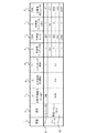
図1は、式(1)で示したFOMをインバータに対して適用した結果の一例を示すものである。 FIG. 1 shows an example of a result obtained by applying the FOM represented by Expression (1) to an inverter.
図1において、1は用途であり対象製品を示し、ここではインバータとしている。2は対象製品において適用される基板の種類を示し、ここではシリコン(Si)基板2aと炭化シリコン(SiC)基板2bを対象にしている。シリコン基板は、広く流通している基板である。一方、炭化シリコン基板は、次世代として期待されている基板である。式(1)で示したFOMは、このような基板材料の選択の際に利用価値が高い。3は電気特性の1つである定格電流密度Jc(A/cm2)である。4は電気特性の1つである定常損失VFであり、DC損失である。5は電気特性の1つであるスイッチング損失errである。6は半導体チップコストCを示している。7は半導体チップに対するFOMを示している。同様に、8は半導体チップを搭載した半導体モジュールコストCを示しており、また9は半導体モジュールに対するFOMを示している。
In FIG. 1,
定格電流密度3は絶対値で示している。通常、シリコン基板2aの定格電流密度3は200〜250A/cm2であり、炭化シリコン基板2bの定格電流密度3は300〜1000A/cm2である。図1では、定格電流密度3を、シリコン基板2aの場合で200A/cm2とし、炭化シリコン基板2bの場合で1000A/cm2としている。
The rated
定常損失4は相対値で示している。ここではシリコン基板2aの定常損失4を1とする。この時、炭化シリコン基板2bの定常損失4は0.6〜0.8となる。図1では、炭化シリコン基板2bの定常損失4を0.8としている。
The steady loss 4 is shown as a relative value. Here, the steady loss 4 of the silicon substrate 2a is 1. At this time, the steady loss 4 of the
スイッチング損失5は相対値で示している。ここではシリコン基板2aのスイッチング損失5を1とする。この時、炭化シリコン基板2bのスイッチング損失5は0.1〜0.3となる。図1では、炭化シリコン基板2bのスイッチング損失5を0.1としている。
The
半導体チップコスト6は相対値で示している。ここではシリコン基板2aの半導体チップコスト6を1とする。この時の炭化シリコン基板2bの半導体チップコスト6は100から1の範囲で示している。図1では、炭化シリコン基板2bの半導体チップコスト6を100、10、5および1として示しているが、実際には連続した値となる。ここで、炭化シリコン基板2bの半導体チップコスト6である100は、半導体チップコストが、シリコン基板2aの半導体チップコスト6より100倍高いことを示す。また炭化シリコン基板2bの半導体チップコスト6である1は、半導体チップコストが、シリコン基板2aの半導体チップコスト6と同等であることを示す。炭化シリコン基板2bの半導体チップコスト6の低下は、例えば、材料調達コストの低下や製造技術の進歩による製造コストの低下により達成される。
The semiconductor chip cost 6 is shown as a relative value. Here, the semiconductor chip cost 6 of the silicon substrate 2a is 1. The semiconductor chip cost 6 of the
半導体チップのFOM7は、式(1)に、シリコン基板2aおよび炭化シリコン基板2bにおける定格電流密度3、定常損失4、スイッチング損失5および半導体チップコスト6の値を代入して計算した値である。
The FOM7 of the semiconductor chip is a value calculated by substituting the values of the rated
半導体モジュールコスト8は、半導体チップコスト6に2を加算したものである。半導体モジュールは、半導体チップを搭載しパッケージにして製造される。そのため半導体モジュールコスト8は、この半導体モジュールの製造に係るコストの割合を半導体チップコスト6に加えたものとなる。ここでは、シリコン基板2aの半導体モジュールコスト8は、半導体チップコスト6に2を加算し3で示し、炭化シリコン基板2bの半導体モジュールコスト8は、半導体チップコスト6に2を加算し102から3の範囲で示している。図1では、炭化シリコン基板2bの半導体モジュールコスト8を102、12、7および3として示しているが、実際には連続した値となる。炭化シリコン基板2bの半導体モジュールコスト8の低下は、例えば、材料調達コストの低下や製造技術の進歩による製造コストの低下により達成される。
The semiconductor module cost 8 is obtained by adding 2 to the semiconductor chip cost 6. A semiconductor module is manufactured by mounting a semiconductor chip into a package. Therefore, the semiconductor module cost 8 is obtained by adding the cost ratio for manufacturing the semiconductor module to the semiconductor chip cost 6. Here, the semiconductor module cost 8 of the silicon substrate 2 a is indicated by 3 by adding 2 to the semiconductor chip cost 6, and the semiconductor module cost 8 of the
半導体モジュールのFOM9は、式(1)に、シリコン基板2aおよび炭化シリコン基板2bにおける定格電流密度3、定常損失4、スイッチング損失5および半導体モジュールコスト8の値を代入して計算した値である。
The FOM 9 of the semiconductor module is a value calculated by substituting the values of the rated
図1に示した半導体チップのFOM7および半導体モジュールのFOM9は次のように用いる。
The
まず、半導体チップのFOM7について説明する。
半導体チップのFOM7は、その値が大きい方が有利となる。即ち、半導体チップのFOM7の数値が大きい方が、性能を満足することはもちろんのこと、低コスト化が図られた製品を市場に投入出来ることになるため、市場での競争力向上に繋がり商業的に有利となる。
First, the
The semiconductor chip FOM7 is advantageous when the value is large. In other words, the larger the value of FOM7 for semiconductor chips, the more satisfactory the performance, as well as the introduction of low-cost products into the market, leading to improved competitiveness in the market. This is advantageous.
図1を見ると、シリコン基板2aを用いた場合の半導体チップのFOM7は200である。これに対し、炭化シリコン基板2aを用いた場合の半導体チップのFOMは、まず半導体チップコスト6が100の場合では125となり、これはシリコン基板2aを用いた場合の半導体チップのFOM7の200より小さいので、この場合は、基板2としてシリコン基板2aを用いて半導体チップを製造した方が、低コスト化が図られた半導体チップを得ることができる。次に、炭化シリコン基板2bの半導体チップコスト6が10の場合は、半導体チップのFOM7が1250となり、これはシリコン基板2aを用いた場合の半導体チップのFOM7の200より大きいので、この場合は、基板2として炭化シリコン基板2bを用いて半導体チップを製造した方が、低コスト化が図られた半導体チップを得ることができる。同様に、炭化シリコン基板2bの半導体チップコスト6が5および1の場合も、炭化シリコン基板2bを用いて半導体チップを製造した方が、低コスト化が図られた半導体チップを得ることができる。なお、炭化シリコン基板2bを用いた場合の半導体チップコスト6が62.5の場合に、半導体チップのFOM7がシリコン基板2aを用いた場合の半導体チップのFOM7と同じ200となる。よって、炭化シリコン基板2bにおける半導体チップコスト6である62.5が、シリコン基板2aまたは炭化シリコン基板2bを使用する際の基準値となる。
Referring to FIG. 1, the
実際の製造においては、半導体チップを製造する際の基板2の選別に使用できる。例えば、シリコン基板2aまたは炭化シリコン基板2bの何れを用いても、所定の性能を満足する半導体チップが得られるとすれば、製造にかかるコストが安いほうが、半導体チップのコストを低減することができる。この場合、シリコン基板2aを用いた場合の半導体チップのFOM7と炭化シリコン基板2bを用いた場合の半導体チップのFOM7とを比較し、望ましい基板2として、半導体チップのFOM7の大きい方の基板2を用いて半導体チップを製造すれば、低コスト化が図られた半導体チップを得ることができる。よって、半導体チップを製造する過程において、シリコン基板2aを用いた場合の半導体チップのFOM7と炭化シリコン基板2bを用いた場合の半導体チップのFOM7とを比較する比較工程と、この比較工程により、所望の基板2として半導体チップのFOM7が大きい基板2を選別する選別工程と、この選別工程により選別された基板2に、半導体素子、例えば、ダイオード,MOSFET,IGBT(Insulated Gate Bipolor Transistor)などのダイオード素子やトランジスタ素子を形成する素子形成工程を備えることにより半導体チップを製造すれば、性能を満足することに加え、低コスト化が図られた半導体チップを得ることができる。このことは市場での競争力向上に繋がり商業的に有利となる。
In actual manufacture, it can be used for sorting the substrates 2 when manufacturing semiconductor chips. For example, if a semiconductor chip that satisfies a predetermined performance can be obtained using either the silicon substrate 2a or the
次に、半導体モジュールのFOM9について説明する。
半導体モジュールのFOM9は、半導体チップのFOM7と同様に、その値が大きい方が有利となる。即ち、半導体モジュールのFOM9の数値が大きい方が、性能を満足することはもちろんのこと、低コスト化が図られた製品を市場に投入出来ることになるため、市場での競争力向上に繋がり商業的に有利となる。
Next, the FOM 9 of the semiconductor module will be described.
As the FOM 9 of the semiconductor module is the same as the
図1を見ると、シリコン基板2aを用いた場合の半導体モジュールのFOM9は67である。これに対し、炭化シリコン基板2bを用いた場合の半導体モジュールのFOM9は、半導体モジュールコスト8が102の場合では123となり、これはシリコン基板2aを用いた場合の半導体モジュールのFOM9の67より大きいので、基板2として炭化シリコン基板2bを用いて半導体モジュールを製造した方が、低コスト化が図られた半導体モジュールを得ることができる。同様に、炭化シリコン基板2bの半導体モジュールコスト8が12,7および3の場合も、炭化シリコン基板2bを用いて半導体モジュールを製造した方が、低コスト化が図られた半導体モジュールを得ることができる。なお、炭化シリコン基板2bを用いた場合の半導体モジュールコスト8が186.57の場合に、半導体モジュールのFOM9がシリコン基板2aを用いた場合の半導体モジュールのFOM9とほぼ同じ67となる。よって、炭化シリコン基板2bにおける半導体モジュールコスト8である186.57が、シリコン基板2aまたは炭化シリコン基板2bを使用する際の基準値となる。なお炭化シリコン基板2bにおける半導体モジュールコスト8が186.57の場合には、半導体チップコスト6は184.57となるので、半導体モジュールを製造する場合には、半導体チップコスト6はほぼ184.57まで許容される。
Referring to FIG. 1, the FOM 9 of the semiconductor module when the silicon substrate 2a is used is 67. On the other hand, the FOM9 of the semiconductor module when the
実際の製造においては、半導体モジュールを製造する際の基板2の選別に使用できる。例えば、シリコン基板2aまたは炭化シリコン基板2bの何れを用いても、所定の性能を満足する半導体モジュールが得られるとすれば、製造にかかるコストが安いほうが、半導体モジュールのコストを低減することができる。この場合、シリコン基板2aを用いた場合の半導体モジュールのFOM9と炭化シリコン基板2bを用いた場合の半導体モジュールのFOM9とを比較し、望ましい基板2として、半導体モジュールのFOM9の大きい方の基板2を用いて半導体モジュールを製造すれば、低コスト化が図られた半導体モジュールを得ることができる。よって、半導体モジュールを製造する過程において、シリコン基板2aを用いた場合の半導体モジュールのFOM9と炭化シリコン基板2bを用いた場合の半導体モジュールのFOM9とを比較する比較工程と、この比較工程により、所望の基板2として半導体モジュールのFOM9が大きい基板2を選別する選別工程とを備えて、この選別工程により選別された基板2に、ダイオード,MOSFET,IGBTなどの半導体素子を形成して半導体チップを製造し、この半導体素子を形成する素子形成工程を経て得られた複数の半導体チップを搭載し結線したのち、パッケージに収納するパッケージ工程を用いて半導体モジュールを製造すれば、性能を満足することに加え、低コスト化が図られた半導体モジュールを得ることができる。このことは市場での競争力向上に繋がり商業的に有利となる。
In actual manufacture, it can be used for selecting the substrate 2 when manufacturing a semiconductor module. For example, if a semiconductor module satisfying a predetermined performance can be obtained using either the silicon substrate 2a or the
なお、この実施の形態においては、対象製品としてインバータを例にして説明をしたが、当然のことながら、インバータに限定されるものではなく、例えば、コンバータ,PFC(Power Factor Control)回路,ブレーキ回路などの他の製品にも適用可能である。 In this embodiment, the inverter has been described as an example of the target product. However, as a matter of course, the present invention is not limited to the inverter. For example, a converter, a PFC (Power Factor Control) circuit, a brake circuit, etc. It is applicable to other products such as.
なお、この実施の形態においては、シリコン基板2a又は炭化シリコン基板2bを例にして説明をしたが、当然のことながら、これらの基板に限定されるものではなく、考えうる全ての基板について、この発明は適用可能である。
In this embodiment, the silicon substrate 2a or the
また、この実施の形態においては、電気的な特性を示す定格電流密度3、定常損失4およびスイッチング損失5に対して所定の数値を用いて説明したが、これらの数値は固定値ではなく所定の範囲を有するものであり、当然のことながら、これらの数値は所定の範囲内で適宜選択されるものである。
In this embodiment, the rated
1 用途(対象製品)、2 基板、2a シリコン基板、2b 炭化シリコン基板、3 定格電流密度、4 定常損失、5 スイッチング損失、6 半導体チップコスト、7 半導体チップのFOM、8 半導体モジュールコスト、9 半導体モジュールのFOM 1 Application (target product), 2 substrate, 2a silicon substrate, 2b silicon carbide substrate, 3 rated current density, 4 steady loss, 5 switching loss, 6 semiconductor chip cost, 7 semiconductor chip FOM, 8 semiconductor module cost, 9 semiconductor Module FOM
Claims (4)
この比較工程による前記計算結果の大小に基づいて、前記種類の異なる基板から所望の基板を選択する選択工程と、
この選択工程により選択された前記所望の基板に半導体素子を形成する素子形成工程とを備え、
前記電気的な性能を示す項は、定格電流密度をJc、定常損失をVF、スイッチング損失をerrとした時に、
Jc/(VF・err)
として表され、
前記半導体チップコストを示す項は、前記半導体チップコストをCとした時に、
1/C
として表され、
前記所望の基板は、前記種類の異なる基板に対する前記FOMの計算結果が大きい方の基板であることを特徴とする半導体チップの製造方法。 Based on the FOM of the semiconductor chip determined as the product of the term indicating the electrical performance of the substrate and the term indicating the semiconductor chip cost, the FOM of the semiconductor chip on different types of substrates is calculated, and the magnitude of the calculation result is calculated. A comparison process to compare;
A selection step of selecting a desired substrate from the different types of substrates based on the magnitude of the calculation result by the comparison step;
An element formation step of forming a semiconductor element on the desired substrate selected by the selection step ,
The terms indicating the electrical performance are as follows: when the rated current density is Jc, the steady loss is VF, and the switching loss is err.
Jc / (VF ・ err)
Represented as
The term indicating the semiconductor chip cost is when the semiconductor chip cost is C,
1 / C
Represented as
The method of manufacturing a semiconductor chip, wherein the desired substrate is a substrate having a larger FOM calculation result for the different types of substrates .
この比較工程による前記計算結果の大小に基づいて、前記種類の異なる基板から所望の基板を選択する選択工程と、
この選択工程により選択された前記所望の基板に半導体素子を形成する素子形成工程と、
この素子形成工程を経て得られた複数の半導体チップを結線しパッケージに収納するパッケージ工程とを備え、
前記電気的な性能を示す項は、定格電流密度をJc、定常損失をVF、スイッチング損失をerrとした時に、
Jc/(VF・err)
として表され、
前記半導体モジュールコストを示す項は、前記半導体モジュールコストをCとした時に、
1/C
として表され、
前記所望の基板は、前記種類の異なる基板に対する前記FOMの計算結果が大きい方の基板である
ことを特徴とする半導体モジュールの製造方法。 Based on the FOM of the semiconductor module determined as the product of the term indicating the electrical performance of the substrate and the term indicating the semiconductor module cost, the FOM of the semiconductor module on different types of substrates is calculated, and the magnitude of the calculation result is calculated. A comparison process to compare;
A selection step of selecting a desired substrate from the different types of substrates based on the magnitude of the calculation result by the comparison step;
An element formation step of forming a semiconductor element on the desired substrate selected by the selection step;
A package process for connecting a plurality of semiconductor chips obtained through the element formation process and storing the semiconductor chips in a package;
The terms indicating the electrical performance are as follows: when the rated current density is Jc, the steady loss is VF, and the switching loss is err.
Jc / (VF ・ err)
Represented as
The term indicating the semiconductor module cost is when the semiconductor module cost is C,
1 / C
Represented as
The desired substrate is a substrate having a larger FOM calculation result for the different types of substrates.
A method for manufacturing a semiconductor module .
Priority Applications (3)
| Application Number | Priority Date | Filing Date | Title |
|---|---|---|---|
| JP2008243438A JP5452003B2 (en) | 2008-09-23 | 2008-09-23 | Semiconductor chip manufacturing method and semiconductor module manufacturing method |
| US12/479,248 US7989227B2 (en) | 2008-09-23 | 2009-06-05 | Method of manufacturing semiconductor chip and semiconductor module |
| DE102009034449.7A DE102009034449B4 (en) | 2008-09-23 | 2009-07-23 | Method for producing a semiconductor chip and a semiconductor module |
Applications Claiming Priority (1)
| Application Number | Priority Date | Filing Date | Title |
|---|---|---|---|
| JP2008243438A JP5452003B2 (en) | 2008-09-23 | 2008-09-23 | Semiconductor chip manufacturing method and semiconductor module manufacturing method |
Publications (2)
| Publication Number | Publication Date |
|---|---|
| JP2010080460A JP2010080460A (en) | 2010-04-08 |
| JP5452003B2 true JP5452003B2 (en) | 2014-03-26 |
Family
ID=42038074
Family Applications (1)
| Application Number | Title | Priority Date | Filing Date |
|---|---|---|---|
| JP2008243438A Active JP5452003B2 (en) | 2008-09-23 | 2008-09-23 | Semiconductor chip manufacturing method and semiconductor module manufacturing method |
Country Status (3)
| Country | Link |
|---|---|
| US (1) | US7989227B2 (en) |
| JP (1) | JP5452003B2 (en) |
| DE (1) | DE102009034449B4 (en) |
Families Citing this family (2)
| Publication number | Priority date | Publication date | Assignee | Title |
|---|---|---|---|---|
| US9147637B2 (en) * | 2011-12-23 | 2015-09-29 | Infineon Technologies Ag | Module including a discrete device mounted on a DCB substrate |
| US9738195B2 (en) * | 2015-01-23 | 2017-08-22 | David John Willis | Automotive center console armrest storage box lid protector |
Family Cites Families (10)
| Publication number | Priority date | Publication date | Assignee | Title |
|---|---|---|---|---|
| JPH0878439A (en) * | 1994-09-05 | 1996-03-22 | Mitsubishi Electric Corp | Method for manufacturing semiconductor device |
| US5493231A (en) * | 1994-10-07 | 1996-02-20 | University Of North Carolina | Method and apparatus for measuring the barrier height distribution in an insulated gate field effect transistor |
| WO1998045719A1 (en) * | 1997-04-04 | 1998-10-15 | University Of Florida | Method for testing and diagnosing mos transistors |
| US7462910B1 (en) | 1998-10-14 | 2008-12-09 | International Rectifier Corporation | P-channel trench MOSFET structure |
| US6621121B2 (en) | 1998-10-26 | 2003-09-16 | Silicon Semiconductor Corporation | Vertical MOSFETs having trench-based gate electrodes within deeper trench-based source electrodes |
| JP4198469B2 (en) | 2001-04-11 | 2008-12-17 | シリコン・セミコンダクター・コーポレイション | Power device and manufacturing method thereof |
| GB0327793D0 (en) | 2003-11-29 | 2003-12-31 | Koninkl Philips Electronics Nv | Trench mosfet |
| US7902049B2 (en) * | 2004-01-27 | 2011-03-08 | United Solar Ovonic Llc | Method for depositing high-quality microcrystalline semiconductor materials |
| JP4744958B2 (en) | 2005-07-13 | 2011-08-10 | 株式会社東芝 | Semiconductor device and manufacturing method thereof |
| JP5017865B2 (en) | 2006-01-17 | 2012-09-05 | 富士電機株式会社 | Semiconductor device |
-
2008
- 2008-09-23 JP JP2008243438A patent/JP5452003B2/en active Active
-
2009
- 2009-06-05 US US12/479,248 patent/US7989227B2/en active Active
- 2009-07-23 DE DE102009034449.7A patent/DE102009034449B4/en active Active
Also Published As
| Publication number | Publication date |
|---|---|
| JP2010080460A (en) | 2010-04-08 |
| US20100075444A1 (en) | 2010-03-25 |
| US7989227B2 (en) | 2011-08-02 |
| DE102009034449A1 (en) | 2010-05-12 |
| DE102009034449B4 (en) | 2016-02-04 |
Similar Documents
| Publication | Publication Date | Title |
|---|---|---|
| Liu | Power electronic packaging: design, assembly process, reliability and modeling | |
| US9721875B2 (en) | Power module and fabrication method for the same | |
| Marcinkowski | Dual-sided cooling of power semiconductor modules | |
| JP2011258623A (en) | Power semiconductor system | |
| Degrenne et al. | A review of prognostics and health management for power semiconductor modules | |
| CN101853847A (en) | Combined semiconductor rectifying device and electric power converter using the combined semiconductor rectifying device | |
| US12500201B2 (en) | Semiconductor element bonding substrate, semiconductor device, and power conversion device | |
| JP6652802B2 (en) | Semiconductor device and inverter device including the semiconductor device | |
| CN110299350A (en) | Semiconductor device | |
| US20230207431A1 (en) | Semiconductor device | |
| JPWO2017183580A1 (en) | Semiconductor device, power module and manufacturing method thereof | |
| CN103081327B (en) | Rectifier device with Schottky diode | |
| Morroni et al. | Understanding the trade-offs and technologies to increase power density | |
| JP5452003B2 (en) | Semiconductor chip manufacturing method and semiconductor module manufacturing method | |
| Liu | Trends of power semiconductor wafer level packaging | |
| Hower et al. | Current status and future trends in silicon power devices | |
| Tang et al. | Degradation in electrothermal characteristics of 4H-SiC junction barrier Schottky diodes under high temperature power cycling stress | |
| Liang et al. | Advanced packaging of SiC power module for automotive applications | |
| Majumdar | Recent technologies and trends of power devices | |
| Siemieniec et al. | Development of low-voltage power MOSFET based on application requirement analysis | |
| US20230207541A1 (en) | Semiconductor device | |
| Narazaki et al. | Direct beam lead bonding for trench MOSFET & CSTBT | |
| JP6269417B2 (en) | Semiconductor device | |
| Toyoshima et al. | Compact SiC power module for high speed switching | |
| Galiev et al. | Optimization of Liquid Cooling Double-layer Heatsink for SiC Power Modules |
Legal Events
| Date | Code | Title | Description |
|---|---|---|---|
| A621 | Written request for application examination |
Free format text: JAPANESE INTERMEDIATE CODE: A621 Effective date: 20101022 |
|
| A131 | Notification of reasons for refusal |
Free format text: JAPANESE INTERMEDIATE CODE: A131 Effective date: 20130226 |
|
| A977 | Report on retrieval |
Free format text: JAPANESE INTERMEDIATE CODE: A971007 Effective date: 20130228 |
|
| RD01 | Notification of change of attorney |
Free format text: JAPANESE INTERMEDIATE CODE: A7421 Effective date: 20130228 |
|
| A521 | Request for written amendment filed |
Free format text: JAPANESE INTERMEDIATE CODE: A523 Effective date: 20130415 |
|
| TRDD | Decision of grant or rejection written | ||
| A01 | Written decision to grant a patent or to grant a registration (utility model) |
Free format text: JAPANESE INTERMEDIATE CODE: A01 Effective date: 20131203 |
|
| A61 | First payment of annual fees (during grant procedure) |
Free format text: JAPANESE INTERMEDIATE CODE: A61 Effective date: 20131227 |
|
| R150 | Certificate of patent or registration of utility model |
Ref document number: 5452003 Country of ref document: JP Free format text: JAPANESE INTERMEDIATE CODE: R150 Free format text: JAPANESE INTERMEDIATE CODE: R150 |
|
| R250 | Receipt of annual fees |
Free format text: JAPANESE INTERMEDIATE CODE: R250 |
|
| R250 | Receipt of annual fees |
Free format text: JAPANESE INTERMEDIATE CODE: R250 |
|
| R250 | Receipt of annual fees |
Free format text: JAPANESE INTERMEDIATE CODE: R250 |
|
| R250 | Receipt of annual fees |
Free format text: JAPANESE INTERMEDIATE CODE: R250 |
|
| R250 | Receipt of annual fees |
Free format text: JAPANESE INTERMEDIATE CODE: R250 |
|
| R250 | Receipt of annual fees |
Free format text: JAPANESE INTERMEDIATE CODE: R250 |
|
| R250 | Receipt of annual fees |
Free format text: JAPANESE INTERMEDIATE CODE: R250 |
|
| R250 | Receipt of annual fees |
Free format text: JAPANESE INTERMEDIATE CODE: R250 |
|
| R250 | Receipt of annual fees |
Free format text: JAPANESE INTERMEDIATE CODE: R250 |