JP5451237B2 - Image forming apparatus - Google Patents

Image forming apparatus Download PDF

Info

Publication number
JP5451237B2
JP5451237B2 JP2009180054A JP2009180054A JP5451237B2 JP 5451237 B2 JP5451237 B2 JP 5451237B2 JP 2009180054 A JP2009180054 A JP 2009180054A JP 2009180054 A JP2009180054 A JP 2009180054A JP 5451237 B2 JP5451237 B2 JP 5451237B2
Authority
JP
Japan
Prior art keywords
signal
clock
rotation
speed
unit
Prior art date
Legal status (The legal status is an assumption and is not a legal conclusion. Google has not performed a legal analysis and makes no representation as to the accuracy of the status listed.)
Active
Application number
JP2009180054A
Other languages
Japanese (ja)
Other versions
JP2011033833A (en
Inventor
克之 山▲崎▼
Current Assignee (The listed assignees may be inaccurate. Google has not performed a legal analysis and makes no representation or warranty as to the accuracy of the list.)
Canon Inc
Original Assignee
Canon Inc
Priority date (The priority date is an assumption and is not a legal conclusion. Google has not performed a legal analysis and makes no representation as to the accuracy of the date listed.)
Filing date
Publication date
Application filed by Canon Inc filed Critical Canon Inc
Priority to JP2009180054A priority Critical patent/JP5451237B2/en
Publication of JP2011033833A publication Critical patent/JP2011033833A/en
Application granted granted Critical
Publication of JP5451237B2 publication Critical patent/JP5451237B2/en
Active legal-status Critical Current
Anticipated expiration legal-status Critical

Links

Images

Landscapes

  • Laser Beam Printer (AREA)
  • Mechanical Optical Scanning Systems (AREA)
  • Control Or Security For Electrophotography (AREA)
  • Facsimile Scanning Arrangements (AREA)
  • Control Of Electric Motors In General (AREA)
  • Control Of Multiple Motors (AREA)

Description

本発明は、一般に電子写真方式の画像形成装置に係り、とりわけ、回転多面鏡を駆動するモータの制御方法に関する。   The present invention generally relates to an electrophotographic image forming apparatus, and more particularly to a method for controlling a motor that drives a rotary polygon mirror.

現在、画像形成装置では、高速・高画質で、かつ多種多様な記録紙に対応可能な装置が求められている。特にカラーの画像形成装置は、複数色の画像を転写体上に順番に重ね合わせてカラー画像を形成するため、より高速で高画質に画像を形成することが要求される。   Currently, there is a demand for an image forming apparatus that can handle a wide variety of recording papers with high speed and high image quality. In particular, since a color image forming apparatus forms a color image by sequentially superimposing a plurality of color images on a transfer body, it is required to form an image with higher speed and higher image quality.

高画質化は、白黒、カラーの画像形成装置ともに、記録紙に対する画像の形成位置の精度を高めることで、用紙に対する“位置ずれ”を少なくすることで達成される。カラー画像形成装置では、複数色の画像を1つの転写体上に重ね合わせる際の位置の精度を高めて各色の“色ずれ”を少なくすることで、高画質化を達成している。   High image quality can be achieved by reducing the “positional deviation” with respect to the paper by increasing the accuracy of the image formation position on the recording paper in both monochrome and color image forming apparatuses. In a color image forming apparatus, high image quality is achieved by increasing the accuracy of the position when superimposing a plurality of color images on one transfer body to reduce the “color shift” of each color.

特許文献1に記載されたポリゴンモータ制御方法では、回転速度制御と回転位相制御とを併用することで、高画質画像形成に必要な高精度の回転制御を実現している。これと併用可能な技術として、特許文献2では、ポリゴンミラーモータの回転速度の変更技術(倍率変更技術)が提案されている。   In the polygon motor control method described in Patent Document 1, high-precision rotation control necessary for high-quality image formation is realized by using both rotation speed control and rotation phase control. As a technique that can be used in combination with this, Patent Document 2 proposes a technique for changing the rotational speed of the polygon mirror motor (magnification changing technique).

特開2003−079175号公報JP 2003-079175 A 特開2007−179005号公報JP 2007-179005 A

しかし、さらなる画像形成位置の精度を向上させるためには、ポリゴンモータの回転速度の微調整幅をより細かくすること(高分解能化)が必要となる。モータ回転制御の目標状態を指し示す信号(GBD)の周期は、例えば、0.001%程度以下の微小な幅で調整できることが望ましい。なお、0.001%は、A3用紙(長手方向の長さ:420mm)であれば、0.04mmに相当する。このような高分解能を実現するためには、例えば、10万カウンタ回路などの高周波回路が必要となってしまう。よって、単一の発振器では、高周波かつ大規模な回路となってしまうため、技術的に困難な上にコスト上も好ましくない。さらに、このような高周波回路を導入すると、信号の受け渡しにクロックの非同期問題が発生しやすい。その結果、制御精度が劣化したり、電気的な外乱ノイズ耐性が劣化したりして、形成される画像の品質が低下する可能性がある。   However, in order to further improve the accuracy of the image forming position, it is necessary to make the fine adjustment range of the rotational speed of the polygon motor finer (higher resolution). It is desirable that the period of the signal (GBD) indicating the target state of the motor rotation control can be adjusted with a minute width of about 0.001% or less, for example. Note that 0.001% corresponds to 0.04 mm for A3 paper (length in the longitudinal direction: 420 mm). In order to realize such a high resolution, for example, a high-frequency circuit such as a 100,000 counter circuit is required. Therefore, a single oscillator is a high-frequency and large-scale circuit, which is technically difficult and not preferable in terms of cost. Furthermore, when such a high-frequency circuit is introduced, a clock asynchronous problem is likely to occur in signal transfer. As a result, there is a possibility that the quality of an image to be formed is deteriorated due to deterioration in control accuracy or deterioration in electrical disturbance noise resistance.

そこで、本発明は、このような課題および他の課題のうち、少なくとも1つを解決することを目的とする。例えば、本発明は、回転多面鏡における回転速度の微調整幅の高分解能化と、回路の規模の簡略化とを両立させることを目的とする。なお、他の課題については明細書の全体を通して理解できよう。   Therefore, an object of the present invention is to solve at least one of such problems and other problems. For example, an object of the present invention is to achieve both high resolution of the fine adjustment width of the rotation speed in the rotary polygon mirror and simplification of the circuit scale. Other issues can be understood throughout the specification.

本発明の画像形成装置は、例えば、回転多面鏡、回転多面鏡を駆動する駆動手段、回転状態検知手段、第1クロック生成手段、回転基準信号生成手段、第2クロック生成手段、受信手段、位相差測定手段および位相差測定手段を備える。回転状態検知手段は、回転多面鏡の回転状態を検知し、回転状態を示す回転状態信号を出力する。第1クロック生成手段は、第1クロックを生成する。回転基準信号生成手段は、第1クロックにしたがって順序回路動作を行い、回転多面鏡の回転基準となる回転基準信号を生成する。第2クロック生成手段は、回転基準信号の周期よりも短く、かつ、第1クロックの周期よりも長い周期の第2クロックを生成する。受信手段は、第2クロックにしたがって順序回路動作を行い、回転基準信号を受信する。位相差測定手段は、第2クロックにしたがって回転状態信号と回転基準信号との位相差を測定する。制御手段は、位相差に基づいて駆動手段に加速信号または減速信号を供給する。   The image forming apparatus of the present invention includes, for example, a rotary polygon mirror, a drive unit that drives the rotary polygon mirror, a rotation state detection unit, a first clock generation unit, a rotation reference signal generation unit, a second clock generation unit, a reception unit, A phase difference measuring unit and a phase difference measuring unit are provided. The rotation state detection means detects the rotation state of the rotary polygon mirror and outputs a rotation state signal indicating the rotation state. The first clock generation means generates a first clock. The rotation reference signal generation means performs a sequential circuit operation according to the first clock, and generates a rotation reference signal that serves as a rotation reference for the rotary polygon mirror. The second clock generation means generates a second clock having a cycle shorter than the cycle of the rotation reference signal and longer than the cycle of the first clock. The receiving means performs a sequential circuit operation according to the second clock and receives the rotation reference signal. The phase difference measuring means measures the phase difference between the rotation state signal and the rotation reference signal according to the second clock. The control means supplies an acceleration signal or a deceleration signal to the driving means based on the phase difference.

本発明によれば、回転基準信号について高速の第1クロックにしたがって生成することで回転多面鏡における回転速度の微調整幅の高分解能化を達成できる。一方で、受信手段や位相差測定手段は、低速の第2クロックにしたがって動作する。よって、回路の規模の簡略化を達成できる。   According to the present invention, it is possible to achieve a high resolution of the fine adjustment width of the rotation speed in the rotary polygon mirror by generating the rotation reference signal according to the high-speed first clock. On the other hand, the receiving means and the phase difference measuring means operate according to the low-speed second clock. Therefore, simplification of the circuit scale can be achieved.

実施例1におけるレーザスキャナを示した図である。1 is a diagram illustrating a laser scanner in Example 1. FIG. 実施例1における加減速信号生成部197の内部構成の一例を示した図である。It is the figure which showed an example of the internal structure of the acceleration / deceleration signal generation part 197 in Example 1. FIG. 実施例1における逸脱判定部193の内部構造の一例を示した図である。It is the figure which showed an example of the internal structure of the deviation determination part 193 in Example 1. FIG. 実施例1の平均処理部194と目標速度保持部195の内部構造の一例を示した図である。FIG. 6 is a diagram illustrating an example of an internal structure of an average processing unit 194 and a target speed holding unit 195 according to the first embodiment. GBD生成回路190の全体像である。2 is an overall view of a GBD generation circuit 190. 水平同期信号カウンタチャネル1150の構成例を示した図である。5 is a diagram showing a configuration example of a horizontal synchronization signal counter channel 1150. FIG. 水平同期信号発生部1120の構成例を示した図(a)およびパルス整形回路303に入力される水平同期信号と水平同期信号を整形して出力した信号とを示した図(b)である。FIG. 6A is a diagram illustrating a configuration example of the horizontal synchronization signal generation unit 1120, and FIG. 5B is a diagram illustrating a horizontal synchronization signal input to the pulse shaping circuit 303 and a signal obtained by shaping and outputting the horizontal synchronization signal. 1枚目の表面(1面目)に関する水平同期信号カウンタチャネル1150xからの出力信号の一例を示した図である。It is the figure which showed an example of the output signal from the horizontal synchronizing signal counter channel 1150x regarding the surface (1st surface) of the 1st sheet. 実施例1のプリントシーケンスにおけるCPU961の動作フローと各制御部への指示を示した図である。FIG. 6 is a diagram illustrating an operation flow of a CPU 961 and an instruction to each control unit in a print sequence according to the first embodiment. 実施例1のモータ制御における変速例を示した図である。FIG. 3 is a diagram illustrating a shift example in motor control according to the first embodiment.

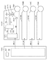
図1は、実施例1におけるレーザスキャナを示した図である。ここでは、4色のトナーを用いて画像を形成する画像形成装置を一例として取り上げて説明する。なお、図中のYMCKは、トナー色であるイエロー、マゼンタ、シアン及びブラックを意味する。参照番号において、各色を区別する必要がある場合には、YMCKを参照番号の末尾に付与するが、区別が必要ない場合はYMCKを省略する。   FIG. 1 is a diagram illustrating a laser scanner according to the first embodiment. Here, an image forming apparatus that forms an image using four color toners will be described as an example. Note that YMCK in the figure means the toner colors yellow, magenta, cyan, and black. In the reference number, when it is necessary to distinguish each color, YMCK is given at the end of the reference number. However, when the distinction is not necessary, YMCK is omitted.

エンジンコントローラ1350は、CPU961及びGBD生成回路190とを備えている。GBDは、モータ回転基準信号の略称とする。モータ回転基準信号(GBD)は、モータ回転制御の目標状態を指し示す信号である。GBDは、繰り返し(周期)信号である。よって、GBDにおける隣り合った2つの立ち下りエッジの間隔がモータの回転周期に対応している。GBDの立下り時刻はモータの回転位相を指し示している。GBDはモータの加速または減速によりフィードバック制御を行う際の速度基準かつ位相基準となる。GBDは、回転検知信号BDと、同一周期となるように設計される。例えば、6面ポリゴンミラーであれば、GBDもBDもポリゴンミラーが1回転するたびに6回の立ち下がりを発生する。また、GBDとBDの差が極力小さくなるようにフィードバック制御が実行される。   The engine controller 1350 includes a CPU 961 and a GBD generation circuit 190. GBD is an abbreviation for motor rotation reference signal. The motor rotation reference signal (GBD) is a signal indicating a target state of motor rotation control. GBD is a repetitive (periodic) signal. Therefore, the interval between two adjacent falling edges in the GBD corresponds to the rotation period of the motor. The falling time of GBD indicates the rotational phase of the motor. GBD serves as a speed reference and phase reference when feedback control is performed by acceleration or deceleration of the motor. GBD is designed to have the same period as rotation detection signal BD. For example, in the case of a six-sided polygon mirror, both the GBD and the BD generate six falles every time the polygon mirror makes one rotation. Further, feedback control is executed so that the difference between GBD and BD is minimized.

CPU961は、エンジンコントローラ1350における主要な制御ユニットである。GBD生成回路190は、CPU961からの指示に応じてGBDを生成する回路である。CPU961は、GBD生成回路190を制御して、YMCKの各色に対応したGBDをモータ回転制御ユニット1310へ出力する。   The CPU 961 is a main control unit in the engine controller 1350. The GBD generation circuit 190 is a circuit that generates a GBD in response to an instruction from the CPU 961. The CPU 961 controls the GBD generation circuit 190 to output GBD corresponding to each color of YMCK to the motor rotation control unit 1310.

モータ回転制御ユニット1310は、レーザ素子から出力されるレーザ光を偏向する回転多面鏡(ポリゴンミラー802)を駆動するDCブラシレスモータを制御するユニットであり、各色ごとに存在する。ポリゴンミラー802によって反射されたレーザ光は、感光ドラム708とBD検知素子803との上を走査することになる。モータ回転制御ユニット1310は、DCブラシレスモータの主な部品は、励磁用の3相励磁コイル1317と、永久磁石ローター1319である。加減速信号生成部197は、GBDと、DCブラシレスモータに取り付けられたホール素子から出力されるホール素子信号FGとに基づいて、加速信号ACCと減速信号DECとを生成して、モータドライバIC1315へ出力する。モータドライバIC1315は、回転多面鏡を駆動する駆動手段の一例であり、加速信号ACCと減速信号DECに基づいて3相信号Pを生成し、DCブラシレスモータに供給する。これにより、DCブラシレスモータの回転速度が目標回転速度へと制御される。なお、モータドライバIC1315は、DCブラシレスモータに取り付けられたホール素子から出力されるホール素子信号FGを増幅して加減速信号生成部197へ供給する。   The motor rotation control unit 1310 is a unit that controls a DC brushless motor that drives a rotary polygon mirror (polygon mirror 802) that deflects laser light output from a laser element, and exists for each color. The laser light reflected by the polygon mirror 802 scans on the photosensitive drum 708 and the BD detection element 803. In the motor rotation control unit 1310, main components of the DC brushless motor are a three-phase excitation coil 1317 for excitation and a permanent magnet rotor 1319. The acceleration / deceleration signal generation unit 197 generates an acceleration signal ACC and a deceleration signal DEC based on the GBD and the Hall element signal FG output from the Hall element attached to the DC brushless motor, and sends it to the motor driver IC 1315. Output. The motor driver IC 1315 is an example of a driving unit that drives the rotary polygon mirror. The motor driver IC 1315 generates a three-phase signal P based on the acceleration signal ACC and the deceleration signal DEC, and supplies it to the DC brushless motor. Thereby, the rotational speed of the DC brushless motor is controlled to the target rotational speed. The motor driver IC 1315 amplifies the Hall element signal FG output from the Hall element attached to the DC brushless motor and supplies the amplified signal to the acceleration / deceleration signal generation unit 197.

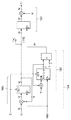
図2は、実施例1における加減速信号生成部197の内部構成の一例を示した図である。GBD生成回路190は、高速クロックXAを発生する順序回路である第1のクロック生成部191から高速クロックXAを供給され、高速クロックXAにしたがって順序回路動作を行う。よって、GBD生成回路190は、第1クロックにしたがって順序回路動作を行い、回転多面鏡の回転基準となる回転基準信号を生成する回転基準信号生成手段の一例である。加減速信号生成部197は、低速クロックXBを生成する順序回路である第2のクロック生成部139から低速クロックXBを供給される。高速クロックXAの周波数は、文字通り、低速クロックXBの周波数よりも高い。また、低速クロックXBの周期は、1回転1発信号Bの周期よりは短い。このように、第1のクロック生成部191は、第1クロックを生成する第1クロック生成手段の一例である。また、第2のクロック生成部139は、回転基準信号の周期よりも短く、かつ、第1クロックの周期よりも長い周期の第2クロックを生成する第2クロック生成手段の一例である。   FIG. 2 is a diagram illustrating an example of an internal configuration of the acceleration / deceleration signal generation unit 197 according to the first embodiment. The GBD generation circuit 190 is supplied with the high-speed clock XA from the first clock generation unit 191 that is a sequential circuit that generates the high-speed clock XA, and performs the sequential circuit operation according to the high-speed clock XA. Therefore, the GBD generation circuit 190 is an example of a rotation reference signal generation unit that performs a sequential circuit operation according to the first clock and generates a rotation reference signal that is a rotation reference of the rotary polygon mirror. The acceleration / deceleration signal generation unit 197 is supplied with the low-speed clock XB from the second clock generation unit 139 which is a sequential circuit that generates the low-speed clock XB. The frequency of the high-speed clock XA is literally higher than the frequency of the low-speed clock XB. Further, the cycle of the low-speed clock XB is shorter than the cycle of one rotation / one-shot signal B. Thus, the first clock generation unit 191 is an example of a first clock generation unit that generates the first clock. The second clock generation unit 139 is an example of a second clock generation unit that generates a second clock having a cycle shorter than the cycle of the rotation reference signal and longer than the cycle of the first clock.

加減速信号生成部197は、主に、ダブルラッチ回路(WLFF)181、平均処理回路180、BD制御部155、FG制御回路141、第1のセレクタ144及び第2のセレクタ145を備えている。BDはビーム検出やビーム検出信号の略称である。ダブルラッチ回路181は、Dフリップフロッップを2段備え、高速クロックXAで動作しているGBD生成回路190から出力されるGBDを入力する。GBD生成回路190は高速クロックXAで動作し、加減速信号生成部197は低速クロックXBで動作している。XAとXBは非同期であるため、これを吸収するために、ダブルラッチ回路181が必要となる。   The acceleration / deceleration signal generation unit 197 mainly includes a double latch circuit (WLFF) 181, an average processing circuit 180, a BD control unit 155, an FG control circuit 141, a first selector 144, and a second selector 145. BD is an abbreviation for beam detection and beam detection signal. The double latch circuit 181 has two stages of D flip-flops, and inputs the GBD output from the GBD generation circuit 190 operating with the high-speed clock XA. The GBD generation circuit 190 operates with the high-speed clock XA, and the acceleration / deceleration signal generation unit 197 operates with the low-speed clock XB. Since XA and XB are asynchronous, a double latch circuit 181 is required to absorb this.

平均処理回路180は、GBDを受信し、単一信号であるGBDから、複数の状態信号を抽出することで、モータ回転制御の目標状態を正しく把握するための回路である。平均処理回路180は、第2クロックにしたがって順序回路動作を行い、回転基準信号を受信する受信手段の一例である。平均処理回路180は、主に、周期計測部192、逸脱判定部193、平均処理部194及び目標速度保持部195を備えている。周期計測部192は、GBDの周期を計測し、周期の計測値Cを、例えば、16bitのデジタルデータとして出力する。周期計測部192は、第2クロックにしたがって回転基準信号の周期を測定する周期測定手段の一例である。逸脱判定部193は、周期の計測値Cが所定の範囲内(例:GMIN=<C=<GMAX)であれば、逸脱していないことを通知するために逸脱判定信号EをLoにする。逸脱判定部193は、周期の計測値Cが所定の範囲外であれば逸脱判定信号EをHiとする。逸脱判定部193は、周期が所定範囲内であるかそれとも所定範囲を逸脱しているかを判定する判定手段の一例である。平均処理部194は、GBDをイネーブルトリガとして16bit値である計測値Cを4回累積加算する。平均処理部194は、周期測定手段が測定した複数の周期の平均値を決定して、平均値を判定手段に供給する平均値決定手段の一例である。平均処理部194は、平均化処理として4回の累積加算が終了すると、それを知らせる信号S4を目標速度保持部195へ出力する。なお、逸脱判定信号EがHiになると、平均処理部194は、累積加算をするカウンタや、累積回数を数えるカウンタをゼロにリセットする。平均処理部194は、周期に応じて回転多面鏡の回転速度の目標速度を決定する目標速度決定手段の一例である。また、平均処理部194は、周期が所定範囲を逸脱していると判定されると、保持手段に保持されている目標速度の変更を抑制する抑制手段としても機能する。目標速度保持部195は、目標速度を保持する保持手段の一例であり、4回目を知らせる信号S4に従って累積結果の下位2bitを切り捨て、上位16bitを保持する。さらに、目標速度保持部195は、上位16bitにポリゴンミラー面数(例:6面)を乗算し、1回転目標速度値を算出して保持する。1回転目標速度値とは、低速クロックXBのカウント量で示される時間に相当する多ビットデータである。この時間は、モータ1回転の目標周期時間に相当する。なお、2bitの切り捨ては「4による除算」であり、平均処理に相当する。よって、高速クロックXAによって最初に示された目標となるBD周期の500usecは、低速クロックXBの4回加算によって「4万カウント前後」の累積値となる。このように、4による除算と面数6の乗算とによって、目標速度保持部195が出力するT1は「6万カウント前後」となる。   The average processing circuit 180 is a circuit for receiving the GBD and extracting a plurality of state signals from the single GBD so as to correctly grasp the target state of the motor rotation control. The average processing circuit 180 is an example of a receiving unit that performs a sequential circuit operation according to a second clock and receives a rotation reference signal. The average processing circuit 180 mainly includes a period measurement unit 192, a departure determination unit 193, an average processing unit 194, and a target speed holding unit 195. The period measurement unit 192 measures the period of GBD and outputs the period measurement value C as, for example, 16-bit digital data. The period measuring unit 192 is an example of a period measuring unit that measures the period of the rotation reference signal according to the second clock. If the measured value C of the period is within a predetermined range (eg, GMIN = <C = <GMAX), the departure determination unit 193 sets the departure determination signal E to Lo to notify that there is no departure. The departure determination unit 193 sets the departure determination signal E to Hi if the cycle measurement value C is outside the predetermined range. The deviation determination unit 193 is an example of a determination unit that determines whether the cycle is within a predetermined range or deviates from the predetermined range. The average processing unit 194 cumulatively adds the measurement value C, which is a 16-bit value, four times using GBD as an enable trigger. The average processing unit 194 is an example of an average value determination unit that determines an average value of a plurality of periods measured by the period measurement unit and supplies the average value to the determination unit. When the four cumulative additions are completed as the averaging process, the average processing unit 194 outputs a signal S4 that informs it to the target speed holding unit 195. Note that when the deviation determination signal E becomes Hi, the average processing unit 194 resets the counter for cumulative addition and the counter for counting the cumulative number to zero. The average processing unit 194 is an example of a target speed determining unit that determines a target speed of the rotational speed of the rotary polygon mirror according to the cycle. In addition, when it is determined that the cycle deviates from the predetermined range, the average processing unit 194 also functions as a suppression unit that suppresses a change in the target speed held in the holding unit. The target speed holding unit 195 is an example of a holding means for holding the target speed, and truncates the lower 2 bits of the accumulated result according to the signal S4 informing the fourth time, and holds the upper 16 bits. Further, the target speed holding unit 195 calculates and holds the one-rotation target speed value by multiplying the upper 16 bits by the number of polygon mirror faces (eg, 6 faces). The single rotation target speed value is multi-bit data corresponding to the time indicated by the count amount of the low-speed clock XB. This time corresponds to a target cycle time for one rotation of the motor. Note that 2-bit truncation is “division by 4”, which corresponds to averaging processing. Therefore, the target BD cycle of 500 usec initially indicated by the high-speed clock XA becomes an accumulated value of “around 40,000 counts” by adding the low-speed clock XB four times. Thus, T1 output from the target speed holding unit 195 becomes “around 60,000 counts” by dividing by 4 and multiplying by 6 faces.

BD制御部155は、GBDから得られる1回転目標速度値と、目標位相と、BDから得られる現在のモータ回転状態との差異から、モータの加減速信号を生成して、その差異が極力小さくなるようにフィードバック制御をするための回路である。BD制御部155は、主に、波形整形部131、分周器151、位相差検知回路152、除算器154、禁止処理回路170、加減算器166、速度差検出器164、二分周器132、立ち上がりエッジ検出器133、立ち下がりエッジ検出器134、ACC信号DEC信号幅生成第1回路135、ACC信号DEC信号幅生成第2回路136、ORゲート回路137、NANDゲート回路138を備えている。波形整形部131は、ダブルラッチによってセンサ信号を低速クロックXBに同期したパルスへと量子化する回路である。分周器151は、入力されたBDをミラー面数(例:6)で分周して、1回転1発信号Bを生成し、後段へ出力する。つまり1回転1発信号Bは、ポリゴンミラーが1回転するごとに1つのパルスとなる信号である。1回転1発信号Bは、ポリゴンミラーの回転状態を示す回転状態信号である。よって、分周器151は、回転多面鏡の回転状態を検知し、回転状態を示す回転状態信号を出力する回転状態検知手段として機能している。位相差検知回路152は、GBDとBを入力し、両者の位相差を示す位相差量T2を算出して出力する。位相差検知回路152は、第2クロックにしたがって回転状態信号と回転基準信号との位相差を測定する位相差測定手段の一例である。除算器154は、位相差量T2にゲイン調整値(例:2−7)を乗算し、ゲイン調整後位相差調整量T3を算出して出力する。除算器154は、位相差に基づいて回転多面鏡の回転位相の制御量を決定する制御量決定手段の一例である。   The BD control unit 155 generates a motor acceleration / deceleration signal from the difference between the one-rotation target speed value obtained from GBD, the target phase, and the current motor rotation state obtained from BD, and the difference is minimized. This is a circuit for performing feedback control. The BD control unit 155 mainly includes a waveform shaping unit 131, a frequency divider 151, a phase difference detection circuit 152, a divider 154, a prohibition processing circuit 170, an adder / subtractor 166, a speed difference detector 164, and a frequency divider 132. An edge detector 133, a falling edge detector 134, an ACC signal DEC signal width generation first circuit 135, an ACC signal DEC signal width generation second circuit 136, an OR gate circuit 137, and a NAND gate circuit 138 are provided. The waveform shaping unit 131 is a circuit that quantizes the sensor signal into a pulse synchronized with the low-speed clock XB by a double latch. The frequency divider 151 divides the input BD by the number of mirror surfaces (for example, 6), generates a single rotation B signal B, and outputs it to the subsequent stage. That is, the one rotation / one-shot signal B is a signal that becomes one pulse every time the polygon mirror makes one rotation. The 1 rotation 1 signal B is a rotation state signal indicating the rotation state of the polygon mirror. Therefore, the frequency divider 151 functions as a rotation state detection unit that detects the rotation state of the rotary polygon mirror and outputs a rotation state signal indicating the rotation state. The phase difference detection circuit 152 inputs GBD and B, calculates and outputs a phase difference amount T2 indicating the phase difference between the two. The phase difference detection circuit 152 is an example of a phase difference measuring unit that measures the phase difference between the rotation state signal and the rotation reference signal in accordance with the second clock. The divider 154 multiplies the phase difference amount T2 by a gain adjustment value (eg, 2-7), and calculates and outputs a gain adjusted phase difference adjustment amount T3. The divider 154 is an example of a control amount determination unit that determines a control amount of the rotational phase of the rotary polygon mirror based on the phase difference.

禁止処理回路170は、T3、E及びモータ速度差信号であるPENを入力し、もし、Eが範囲の逸脱を示していれば、位相制御量T4をゼロに設定する。Eが範囲の逸脱を示していなければ、禁止処理回路170は、ゲイン調整後位相差調整量T3を位相制御量T4として出力する。このように、禁止処理回路170は、周期が所定範囲を逸脱していると判定されると、位相差が制御量に反映されることを抑制する抑制手段として機能する。加減算器166は、T1に対してT4を加減算し、得られた位相差から求められた加減速制御量を目標速度値の調整量として計算する。例えば、GBD信号よりBD信号が遅れているために位相差が加速側の値であれば、減算調整が実行される。逆の場合には、加算調整が実行される。速度差検出器164は、1回転1発信号Bの周期を計測し、その計測値に基づいて位相制御量T4の無効判断をする。例えば、BD信号周期がT3の半周期より長い場合には、位相差が適切に検出されていないと判断する。よって、速度差検出器164は、PEN信号をLoとして出力し、位相制御量T4をゼロに設定する。立ち上がりエッジ検出器133と、立ち下がりエッジ検出器134と、二分周器132は、1回転1発信号Bごとに交互動作するトリガ信号を各々生成する。その結果、ACC信号DEC信号幅生成第1回路135およびACC信号DEC信号幅生成第2回路136が、交互動作する。ACC信号DEC信号幅生成第1回路135は、立ち上がりエッジ検出器133からのトリガ信号でゼロリセットするカウンタであり、リセット時は出力をHiにする。ACC信号DEC信号幅生成第1回路135は、次のクロックからカウントアップして行き、カウント値がT4を超えると出力をLoに変更する。ACC信号DEC信号幅生成第2回路136側も、第1回路と同等の構成であり、1回転1発信号Bにしたがって動作する。ORゲート回路137は、BD信号に基づいた加速信号を生成し、ACC信号DEC信号幅生成第1回路135および第2回路136が両方Hiの時間帯にのみ、加速指示として出力(PACC)をLoにする。NANDゲート回路138は、ACC信号DEC信号幅生成第1回路135および第2回路136が両方Loの時間帯にのみ、減速指示として出力(PDEC)をLoにする。このように、BD制御部155は、位相差に基づいて駆動手段に加速信号または減速信号を供給する制御手段の一例である。   The prohibition processing circuit 170 inputs T3, E and PEN which is a motor speed difference signal, and if E indicates a deviation from the range, sets the phase control amount T4 to zero. If E does not indicate a deviation from the range, the prohibition processing circuit 170 outputs the post-gain adjustment phase difference adjustment amount T3 as the phase control amount T4. As described above, the prohibition processing circuit 170 functions as a suppression unit that suppresses the phase difference from being reflected in the control amount when it is determined that the cycle is out of the predetermined range. The adder / subtractor 166 adds / subtracts T4 to / from T1, and calculates the acceleration / deceleration control amount obtained from the obtained phase difference as the adjustment amount of the target speed value. For example, if the phase difference is an acceleration-side value because the BD signal is delayed from the GBD signal, the subtraction adjustment is executed. In the opposite case, addition adjustment is performed. The speed difference detector 164 measures the period of one rotation / one-shot signal B, and determines invalidity of the phase control amount T4 based on the measured value. For example, when the BD signal cycle is longer than a half cycle of T3, it is determined that the phase difference is not properly detected. Therefore, the speed difference detector 164 outputs the PEN signal as Lo, and sets the phase control amount T4 to zero. The rising edge detector 133, the falling edge detector 134, and the divide-by-two 132 each generate a trigger signal that operates alternately for each revolution B signal B. As a result, the ACC signal DEC signal width generation first circuit 135 and the ACC signal DEC signal width generation second circuit 136 operate alternately. The ACC signal DEC signal width generation first circuit 135 is a counter that resets to zero with a trigger signal from the rising edge detector 133, and sets the output to Hi when reset. The ACC signal DEC signal width generation first circuit 135 counts up from the next clock, and changes the output to Lo when the count value exceeds T4. The ACC signal DEC signal width generation second circuit 136 side also has the same configuration as that of the first circuit, and operates according to the signal B for one rotation. The OR gate circuit 137 generates an acceleration signal based on the BD signal, and outputs the output (PACC) as an acceleration instruction Lo only when the ACC signal DEC signal width generation first circuit 135 and the second circuit 136 are both in the Hi time zone. To. The NAND gate circuit 138 sets the output (PDEC) to Lo as a deceleration instruction only when both the ACC signal DEC signal width generation first circuit 135 and the second circuit 136 are Lo. Thus, the BD control unit 155 is an example of a control unit that supplies an acceleration signal or a deceleration signal to the driving unit based on the phase difference.

BD信号とGBD信号の差異が無くなると、ACC信号DEC信号幅生成第1回路135の出力と第2回路136の出力とは互い違いの値へと同時に遷移するようになる。ORゲート回路137の出力とNANDゲート回路138の出力は両方ともHiを維持するため、加速指示も減速指示も行われなくなる。   When the difference between the BD signal and the GBD signal disappears, the output of the ACC signal DEC signal width generation first circuit 135 and the output of the second circuit 136 transition simultaneously to alternate values. Since both the output of the OR gate circuit 137 and the output of the NAND gate circuit 138 maintain Hi, neither an acceleration instruction nor a deceleration instruction is issued.

FG制御回路141は、FG用1回転目標速度値と、FGから得られる現在のモータ回転状態との差異から、モータの加減速信号に生成して、その差異が極力小さくなるようにフィードバック制御をするための回路である。FG制御回路141は、分周器147、速度差検出器148を備えている。分周器147は、FGを1回転あたりのFG極パルス数で分周し、1回転1発信号Fを生成して、後段へ出力する。FG用の1目標速度値146は、CPU961からの指示に基づく固定レジスタ設定値である。速度差検出器148は、目標速度値146とFを入力し、FG回転速度を計測し、その差異が小さい場合にのみ、FG/BD選択信号SEとしてHiを出力する。なお、FG回転速度は、1回転1発信号Fの信号間隔測定により求められるクロックカウント値である。SEは、出力すべきACCを選択する第1のセレクタ144と、出力すべきDECを選択する第2のセレクタ145とに供給される。第1のセレクタ144は、SEがHiの場合、BD制御部155から出力されてきたACCを選択し、SEがLoの場合、FG制御回路141から出力されてきたACCを選択する。同様に、第2のセレクタ145は、SEがHiの場合、BD制御部155から出力されてきたDECを選択し、SEがLoの場合、FG制御回路141から出力されてきたDECを選択する。   The FG control circuit 141 generates a motor acceleration / deceleration signal from the difference between the FG one-rotation target speed value and the current motor rotation state obtained from the FG, and performs feedback control so that the difference is minimized. It is a circuit for doing. The FG control circuit 141 includes a frequency divider 147 and a speed difference detector 148. The frequency divider 147 divides the FG by the number of FG pole pulses per rotation, generates a single rotation F signal, and outputs it to the subsequent stage. The one target speed value 146 for FG is a fixed register setting value based on an instruction from the CPU 961. The speed difference detector 148 inputs the target speed value 146 and F, measures the FG rotation speed, and outputs Hi as the FG / BD selection signal SE only when the difference is small. The FG rotation speed is a clock count value obtained by measuring the signal interval of one rotation / one-shot signal F. The SE is supplied to a first selector 144 that selects an ACC to be output and a second selector 145 that selects a DEC to be output. The first selector 144 selects the ACC output from the BD control unit 155 when the SE is Hi, and selects the ACC output from the FG control circuit 141 when the SE is Lo. Similarly, the second selector 145 selects the DEC output from the BD control unit 155 when the SE is Hi, and selects the DEC output from the FG control circuit 141 when the SE is Lo.

分周器172は、1回転1発信号Fを2分周して出力する。立ち上がりエッジ検出器173および立ち下がりエッジ検出器174により、分周された1回転1発信号Fの立ち上がりと立ち下がりに対応したパルスが生成される。従って、立ち上がりエッジ検出器173と立ち下がりエッジ検出器174とから交互に1回転1発信号Fが出力される。これらの出力は、17bitカウンタ175、176に交互に入力される。17bitカウンタ175、176は、立ち上がりエッジ検出器173、立ち下がりエッジ検出器174の出力でカウント値をリセットし、基準となる低速クロックCLKを速度目標値までカウントした後、カウントを停止する。これらの出力は、リセット後カウント中はHiで、速度目標値までカウントしたときにLoとなる。17bitカウンタ175、176の出力がLoである時間が、画像形成時の1回転1発信号Fの周期と同じになるように低速クロックCLKと速度目標値とが予め設定されている。17bitカウンタ175、176の出力の論理和をOR回路177で取ることにより、速度系加速信号FACC信号が得られる。また、17bitカウンタ175、176の出力をNANDゲート回路138で取ることにより、速度系減速信号FDEC信号が得られる。   The frequency divider 172 divides the one-shot one-shot signal F by two and outputs it. The rising edge detector 173 and the falling edge detector 174 generate pulses corresponding to the rising and falling edges of the frequency-divided one rotation one-shot signal F. Accordingly, the one-cycle one-shot signal F is alternately output from the rising edge detector 173 and the falling edge detector 174. These outputs are alternately input to 17-bit counters 175 and 176. The 17-bit counters 175 and 176 reset the count values with the outputs of the rising edge detector 173 and the falling edge detector 174, count the reference low-speed clock CLK to the speed target value, and then stop counting. These outputs are Hi during counting after reset and become Lo when the speed target value is counted. The low-speed clock CLK and the speed target value are set in advance so that the time during which the outputs of the 17-bit counters 175 and 176 are Lo is the same as the cycle of the single rotation / one-shot signal F during image formation. By taking the logical sum of the outputs of the 17-bit counters 175 and 176 by the OR circuit 177, a speed system acceleration signal FACC signal is obtained. Further, by taking the outputs of the 17-bit counters 175 and 176 by the NAND gate circuit 138, a speed system deceleration signal FDEC signal is obtained.

図3は、実施例1における逸脱判定部193の内部構造の一例を示した図である。逸脱判定部193は、CPU961からGMAX、GMINおよびCを設定される。GMAXおよびGMINは、回転基準信号の周期を判定するために使用される所定範囲を定義する情報である。すなわち、GMAXは、副走査倍率の微調整範囲の上限値であり、GMINは、副走査倍率の微調整範囲の下限値である。このように、所定範囲は、副走査倍率の微調整範囲に対応して決定された範囲である。一般に、用紙の裏面への画像形成は、表面に画像が形成された後に実行される。表面の定着処理によって用紙が加熱及び加圧されると、用紙が一時的に伸びる。なお、用紙の温度が下がると、用紙は縮み、再度元の大きさに戻る。なお、用紙の素材によっては、加熱と伸縮との関係が正反対の場合もある。よって、裏面と表面とで、同一の副走査倍率にて画像を形成してしまうと、用紙の温度が常温に戻ったときに、表面の画像サイズと裏面の画像サイズとが異なってしまう。用紙の伸縮を考慮して、裏面の倍率は、表面の倍率よりも大きくする必要がある。例えば、副走査倍率の微調整範囲が基準倍率(例:10000XBカウント)の±1%であれば、GMIN=9900、GMAX=10100と設定される。第1の比較器201は、CとGMAXとを比較し、比較結果を論理和回路203に出力する。同様に、第2の比較器202は、CとGMINとを比較し、比較結果を論理和回路203に出力する。論理和回路203は、GMIN=<C=<GMAXが満たされたときにゼロ(Lo)を出力し、そうでなければ1(Hi)を出力する。   FIG. 3 is a diagram illustrating an example of an internal structure of the departure determination unit 193 according to the first embodiment. The departure determination unit 193 is set with GMAX, GMIN, and C from the CPU 961. GMAX and GMIN are information defining a predetermined range used for determining the period of the rotation reference signal. That is, GMAX is the upper limit value of the fine adjustment range of the sub-scanning magnification, and GMIN is the lower limit value of the fine adjustment range of the sub-scanning magnification. Thus, the predetermined range is a range determined in accordance with the fine adjustment range of the sub-scanning magnification. In general, image formation on the back side of a sheet is performed after an image is formed on the front side. When the sheet is heated and pressurized by the surface fixing process, the sheet temporarily extends. When the temperature of the paper decreases, the paper shrinks and returns to the original size again. Depending on the material of the paper, the relationship between heating and expansion / contraction may be the opposite. Therefore, if an image is formed on the back surface and the front surface at the same sub-scanning magnification, the image size on the front surface and the image size on the back surface are different when the paper temperature returns to room temperature. In consideration of the expansion and contraction of the paper, the magnification on the back surface needs to be larger than the magnification on the front surface. For example, if the fine adjustment range of the sub-scanning magnification is ± 1% of the reference magnification (eg, 10000 × B count), GMIN = 9900 and GMAX = 10100 are set. The first comparator 201 compares C and GMAX and outputs the comparison result to the OR circuit 203. Similarly, the second comparator 202 compares C and GMIN and outputs the comparison result to the OR circuit 203. The OR circuit 203 outputs zero (Lo) when GMIN = <C = <GMAX is satisfied, and outputs 1 (Hi) otherwise.

図4は、実施例1の平均処理部194と目標速度保持部195の内部構造の一例を示した図である。回路185は、GBDをイネーブルトリガとして16bitのCを4回累積加算する回路である。回路186は、GBDをイネーブルトリガとして機能する4回のカウンタと比較器とを備え、4回目を知らせる回路である。回路185、186は、逸脱判定信号Eによってリセットされる。目標速度保持部195は、4回目を知らせる信号S4に従って累積結果の下位2bitを切り捨て、上位16bitを保持する。目標速度保持部195は、これにポリゴンミラー面数を乗算して、1目標速度値T1として保持する。   FIG. 4 is a diagram illustrating an example of the internal structure of the average processing unit 194 and the target speed holding unit 195 according to the first embodiment. The circuit 185 is a circuit that accumulates and adds 16 bits of C four times using GBD as an enable trigger. The circuit 186 includes a counter for four times and a comparator functioning as a trigger for GBD, and is a circuit for informing the fourth time. The circuits 185 and 186 are reset by the departure determination signal E. The target speed holding unit 195 truncates the lower 2 bits of the accumulated result according to the signal S4 informing the fourth time, and holds the upper 16 bits. The target speed holding unit 195 multiplies this by the number of polygon mirror surfaces and holds it as one target speed value T1.

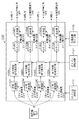
図5は、GBD生成回路190の全体像である。図中の参照符号の末尾に付与したxyzwは、4つのチャネルを区別するために付与した文字であり、省略されることがある。   FIG. 5 is an overall view of the GBD generation circuit 190. The xyzw added at the end of the reference symbol in the figure is a character added to distinguish the four channels and may be omitted.

紙先端信号ITOPは、CPU961によって生成された信号であり、スイッチ1141x、141y、141z、141wに入力される。スイッチ1141x、141y、141z、141wの各出力は、それぞれ水平同期信号カウンタチャネル1150x、1150y、1150z、1150wに入力される。これらの4つのスイッチは、4つの水平同期信号カウンタのどれか1つにITOP信号を順に入力を許可するように機能する。以下では、水平同期信号カウンタチャネルを単にチャネルと称す。1枚目の紙先端では、スイッチ1141xのみがONする。よって、チャネル1150x以降がITOPに応答して動作を開始する。2枚目以降の紙先端から、順次、チャネル1150y、1150z、1150wにITOPが伝達される。   The paper leading edge signal ITOP is a signal generated by the CPU 961 and is input to the switches 1141x, 141y, 141z, and 141w. The outputs of the switches 1141x, 141y, 141z, and 141w are input to horizontal synchronization signal counter channels 1150x, 1150y, 1150z, and 1150w, respectively. These four switches function to allow an ITOP signal to be sequentially input to any one of the four horizontal synchronization signal counters. Hereinafter, the horizontal synchronization signal counter channel is simply referred to as a channel. At the leading edge of the first sheet, only the switch 1141x is turned on. Therefore, the channel 1150x and subsequent channels start to operate in response to ITOP. ITOP is sequentially transmitted to the channels 1150y, 1150z, and 1150w from the leading edge of the second and subsequent sheets.

チャネル1150x、1150y、1150z、1150wは、ITOP信号からタンデム方式の各ドラム間遅延時間を計時し、各色の先端位置信号および水平同期信号を発生する発生回路である。チャネル1150xには、さらに、1ライン以下の遅延量1111x、ポリゴン回転周期1121x、先端位置ライン数1135xが入力される。チャネル1150xは、これらに基づいて、ポリゴン位相制御信号1138x、先端位置信号1137xを後段のセレクタ140へ出力する。1ライン以下の遅延量1111xは、4色のドラム間遅延時間の各々を、当該ページのポリゴン回転周期で割った余り時間である。これは、クロックカウント値としてCPU961から指示される4つのレジスタ設定値である。ポリゴン回転周期1121xは、当該ページの主走査周期である。これは、4色共通で1つのクロックカウント値がCPU961から指示される1つのレジスタ設定値である。先端位置ライン数1135xは、4色のドラム間遅延時間を、当該ページのポリゴン回転周期で割った商の整数である。これも、CPU961から指示される4つのレジスタ設定値である。ポリゴン位相制御信号1138xは、当該ページの4色の各GBDに相当する4本の信号束である。先端位置信号1137xは、当該ページのITOP信号から、所定のドラム間遅延時間を経過した4色の各先端を指し示す4本の信号束である。なお、他のチャネル1150y、1150z、1150wも各ページの特性に対応したレジスタ設定値にて、各々同様に動作する。   Channels 1150x, 1150y, 1150z, and 1150w are generation circuits that measure the tandem delay time between the drums from the ITOP signal and generate a leading edge position signal and a horizontal synchronization signal for each color. Further, a delay amount 1111x of one line or less, a polygon rotation period 1121x, and a tip position line number 1135x are input to the channel 1150x. Based on these, the channel 1150x outputs the polygon phase control signal 1138x and the tip position signal 1137x to the selector 140 at the subsequent stage. The delay amount 1111x of one line or less is a remainder time obtained by dividing each of the four-color inter-drum delay times by the polygon rotation period of the page. This is four register setting values instructed from the CPU 961 as the clock count value. The polygon rotation period 1121x is the main scanning period of the page. This is one register setting value that is common to the four colors and instructed by the CPU 961 as one clock count value. The number of front end position lines 1135x is an integer of a quotient obtained by dividing the delay time between the four colors of drums by the polygon rotation period of the page. This is also four register setting values instructed from the CPU 961. The polygon phase control signal 1138x is a bundle of four signals corresponding to the four colors of GBD of the page. The leading edge position signal 1137x is a bundle of four signals indicating the leading edges of the four colors that have passed a predetermined inter-drum delay time from the ITOP signal of the page. The other channels 1150y, 1150z, and 1150w operate in the same manner with register setting values corresponding to the characteristics of each page.

セレクタ140は、各チャネルから出力されたポリゴン位相制御信号と先端位置信号1137xとに基づいて、上述したGBD信号と先端位置信号1137をモータ回転制御ユニット1310へ出力する。   The selector 140 outputs the GBD signal and the tip position signal 1137 described above to the motor rotation control unit 1310 based on the polygon phase control signal and the tip position signal 1137x output from each channel.

例えば、1枚目を両面印刷し、2枚目は片面印刷する場合に、1枚目の表面(1面目)はチャネル1150xで処理し、1枚目の裏面(2面目)はチャネル1150yで処理し、2枚目の表面(3面目)はチャネル1150z、で処理することができる。   For example, when the first sheet is printed on both sides and the second sheet is printed on one side, the front side (first side) of the first page is processed by channel 1150x and the back side (second side) of the first sheet is processed by channel 1150y. The second surface (third surface) can be processed with the channel 1150z.

図6は、チャネル1150の構成例を示した図である。上述した1ライン以下の遅延量1111、信号遅延部1110、先端位置ライン数1135、及び、ポリゴン回転周期1121は、ドラム間遅延量m0、c0、k0と、両面プリントのそれぞれの副走査倍率に基づいてCPU961が決定する。なお、ドラム間遅延量m0は、感光ドラム708Yに対する感光ドラム708Mについての遅延量である。ドラム間遅延量c0は、感光ドラム708Yに対する感光ドラム708Cについての遅延量である。ドラム間遅延量k0は、感光ドラム708Yに対する感光ドラム708Kについての遅延量である。1ライン以下の遅延量1111Yは、通常、0である。   FIG. 6 is a diagram illustrating a configuration example of the channel 1150. The delay amount 1111 or less, the signal delay unit 1110, the leading position line number 1135, and the polygon rotation period 1121 described above are based on the inter-drum delay amounts m0, c0, k0 and the respective sub-scan magnifications of the duplex printing. CPU 961 determines. The inter-drum delay amount m0 is a delay amount for the photosensitive drum 708M with respect to the photosensitive drum 708Y. The inter-drum delay amount c0 is a delay amount for the photosensitive drum 708C with respect to the photosensitive drum 708Y. The inter-drum delay amount k0 is a delay amount for the photosensitive drum 708K with respect to the photosensitive drum 708Y. The delay amount 1111Y of one line or less is normally zero.

信号遅延部1110は、入力された1ライン以下の遅延量1111に応じて、紙先端信号ITOPを遅延させる回路である。水平同期信号発生部1120は、遅延処理された紙先端信号ITOPと、入力されたポリゴン回転周期1121とに応じてポリゴン位相制御信号(GBD信号)と、先端位置信号を出力する。カウンタ1130は、ポリゴン位相制御信号をカウントする。比較器1136は、カウンタ1130のカウント値と先端位置ライン数1135とを比較し、比較結果に応じて先端位置信号1137を生成して出力する。   The signal delay unit 1110 is a circuit that delays the paper leading edge signal ITOP according to the input delay amount 1111 of one line or less. The horizontal synchronization signal generator 1120 outputs a polygon phase control signal (GBD signal) and a leading edge position signal according to the paper leading edge signal ITOP subjected to delay processing and the inputted polygon rotation period 1121. The counter 1130 counts the polygon phase control signal. The comparator 1136 compares the count value of the counter 1130 with the tip position line number 1135, and generates and outputs a tip position signal 1137 according to the comparison result.

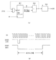
図7(a)は、水平同期信号発生部1120の構成例を示した図である。図7(b)は、パルス整形回路303に入力される水平同期信号と水平同期信号を整形して出力した信号を示した図である。カウンタ回路301は、外部リセットかつ自己リセット付のカウンタである。コンパレータ回路302は、カウンタ回路301から出力された値と、ポリゴン回転周期1121とを比較し、モータ回転の基準となる回転基準同期信号GBDの基となる水平同期信号を生成して出力する。パルス整形回路303は、図7(b)に示すように、水平同期信号をパルス整形して出力する。   FIG. 7A is a diagram illustrating a configuration example of the horizontal synchronization signal generation unit 1120. FIG. 7B is a diagram illustrating a horizontal synchronization signal input to the pulse shaping circuit 303 and a signal output by shaping the horizontal synchronization signal. The counter circuit 301 is a counter with external reset and self-reset. The comparator circuit 302 compares the value output from the counter circuit 301 with the polygon rotation period 1121, and generates and outputs a horizontal synchronization signal that is the basis of the rotation reference synchronization signal GBD that is a reference for motor rotation. As shown in FIG. 7B, the pulse shaping circuit 303 shapes the horizontal synchronization signal and outputs it.

図8は、1枚目の表面(1面目)に関するチャネル1150xからの出力信号の一例を示した図である。4色作像のトリガとなる紙先端信号ITOPが、スイッチ1141xを経由してチャネル1150xに到達する。遅延が0であるから、紙先端信号ITOPを基準に水平同期信号発生部1120xのカウンタ回路301をリセットし、周期信号の発振を開始する。ポリゴン回転周期1121に基づいて、GBDが生成されて出力される。出力されたGBD_Y、GBD_M、GBD_C、GBD_Kは、セレクタ140によって選択されて後段へ出力される。図8において、水平同期信号は立ち下がり基準エッジの部分を縦線のように図示している。この縦線部分の1つ1つは、図7(b)に示すように、40クロック時間(高速クロックXA)のLoパルス信号となっている。   FIG. 8 is a diagram illustrating an example of an output signal from the channel 1150x regarding the first surface (first surface). A paper leading edge signal ITOP that triggers four-color image formation reaches the channel 1150x via the switch 1141x. Since the delay is 0, the counter circuit 301 of the horizontal synchronizing signal generator 1120x is reset based on the paper leading edge signal ITOP, and oscillation of a periodic signal is started. Based on the polygon rotation period 1121, a GBD is generated and output. The output GBD_Y, GBD_M, GBD_C, and GBD_K are selected by the selector 140 and output to the subsequent stage. In FIG. 8, the horizontal synchronizing signal shows the falling reference edge portion as a vertical line. Each vertical line portion is a Lo pulse signal of 40 clock times (high-speed clock XA) as shown in FIG. 7B.

GBD信号150YMCKおのおのがパルス整形回路303によって整形されて出力している。パルス整形回路303で整形するのは、後段の加減速信号生成部197内のダブルラッチ回路181にて、低速クロックXBで信号の遷移タイミングを漏れなく非同期受信できるようにするためである。信号がHiからLoへ遷移するタイミングを基準として扱う設計であるので、GBD信号150は、低速クロックXBの2クロック周期より十分長い間隔で遷移する信号であることが望ましく、40クロック時間より大きくてもよい。   Each of the GBD signals 150YMCK is shaped by the pulse shaping circuit 303 and output. The pulse shaping circuit 303 shapes the signal so that the double latch circuit 181 in the subsequent acceleration / deceleration signal generation unit 197 can asynchronously receive the signal transition timing with the low-speed clock XB. Since the design is based on the timing at which the signal transitions from Hi to Lo, the GBD signal 150 is preferably a signal that transitions at an interval sufficiently longer than two clock cycles of the low-speed clock XB, and is greater than 40 clock hours. Also good.

GBD生成回路190の順序回路は、高速クロックXAで駆動される。すなわち、高速クロックXAの周期を基本単位として、カウントによる時間計測が実行され、各種の信号が生成される。高速クロックXAは、例えば、200MHz(=5ns)であり、水晶発振器によって発振される。   The sequential circuit of the GBD generation circuit 190 is driven by the high-speed clock XA. That is, time measurement is performed by counting with the period of the high-speed clock XA as a basic unit, and various signals are generated. The high-speed clock XA is, for example, 200 MHz (= 5 ns) and is oscillated by a crystal oscillator.

目標となるBD周期は、ポリゴン回転周期1121によって表現される。ポリゴン回転周期1121は、副走査倍率に応じて定められる。プリント用紙の種類に応じて用紙の副走査方向における伸縮率は異なる。よって、CPU961は、プリント用紙の種類に応じて決定したポリゴン回転周期1121を、GBD生成回路190が備えるレジスタに設定する。   The target BD period is expressed by a polygon rotation period 1121. The polygon rotation period 1121 is determined according to the sub-scanning magnification. Depending on the type of print paper, the expansion / contraction ratio in the sub-scanning direction of the paper differs. Therefore, the CPU 961 sets the polygon rotation period 1121 determined according to the type of print paper in a register included in the GBD generation circuit 190.

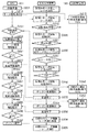
図9は、実施例1のプリントシーケンスにおけるCPU961の動作フローと各制御部への指示を示した図である。ここでは、1枚目は両面印刷を実行し、2枚目は片面印刷を実行するものと仮定する。1枚目表面の周期は、基準値の100%とし、1枚目裏面の周期は101%として、2枚目表面の周期99%と仮定する。図9中の左はCPU961が実行する各ステップを示し、図中の中央はレーザスキャナ制御の状態遷移を示し、図中の右はGBD生成回路190の状態を示している。   FIG. 9 is a diagram illustrating an operation flow of the CPU 961 and an instruction to each control unit in the print sequence according to the first embodiment. Here, it is assumed that double-sided printing is performed on the first sheet and single-sided printing is performed on the second sheet. It is assumed that the period of the first sheet surface is 100% of the reference value, the period of the first sheet back surface is 101%, and the period of the second sheet surface is 99%. The left in FIG. 9 shows the steps executed by the CPU 961, the center in the figure shows the state transition of laser scanner control, and the right in the figure shows the state of the GBD generation circuit 190.

S201で、CPU961は、プリント指示が入力されると、作像準備をする。例えば、PWM(パルス幅変調)の設定など、作造に必要な準備を実行する。   In step S201, when a print instruction is input, the CPU 961 prepares for image formation. For example, preparation necessary for production such as setting of PWM (pulse width modulation) is executed.

S210で、CPU961は、4つの加減速信号生成部197にモータの回転指示を送信する。加減速信号生成部197は、CPU961の指示にしたがってDCモータの回転を開始する。すなわち、加減速信号生成部197は、モータドライバIC1315から入力されたFG信号にしたがってDCモータをフィードバック制御する。これにより、DCモータの回転速度が所望のFG信号回転速度となる。   In step S210, the CPU 961 transmits a motor rotation instruction to the four acceleration / deceleration signal generation units 197. The acceleration / deceleration signal generation unit 197 starts rotating the DC motor in accordance with an instruction from the CPU 961. That is, the acceleration / deceleration signal generation unit 197 feedback-controls the DC motor according to the FG signal input from the motor driver IC 1315. Thereby, the rotational speed of the DC motor becomes a desired FG signal rotational speed.

状態0において、レーザ素子は消灯している。よって、CPU961はレーザ点灯制御を開始するためのAPC(自動光量制御)の設定を開始する。また、CPU961は、感光ドラム708の回転も開始する。   In state 0, the laser element is turned off. Therefore, the CPU 961 starts setting of APC (automatic light quantity control) for starting laser lighting control. The CPU 961 also starts to rotate the photosensitive drum 708.

S215で、CPU961は、両面1面目の副走査倍率に相当するGBD信号を出力するようGBD生成回路190に指示する。   In S215, the CPU 961 instructs the GBD generation circuit 190 to output a GBD signal corresponding to the sub-scan magnification of the first surface of both sides.

ここで、状態0から状態1へと移行する。状態1では、DCモータは回転しているが、レーザ素子は依然として消灯したままである。   Here, transition from state 0 to state 1 occurs. In state 1, the DC motor is rotating, but the laser element is still extinguished.

S212で、加減速信号生成部197は、DCモータの回転速度が安定したか否かを判定する。加減速信号生成部197が備える速度差検出器148は、FG信号が所望の回転速度範囲になったことを示しているか否かを判定する。例えば、FG回転速度が安定するまでに起動からおよそ3sec程度かかる。FG回転速度が安定すると、S220に進む。この時点で状態1から状態2へ遷移する。   In S212, the acceleration / deceleration signal generation unit 197 determines whether or not the rotational speed of the DC motor is stable. The speed difference detector 148 provided in the acceleration / deceleration signal generation unit 197 determines whether or not the FG signal indicates that a desired rotational speed range has been reached. For example, it takes about 3 seconds from startup until the FG rotation speed is stabilized. When the FG rotation speed is stabilized, the process proceeds to S220. At this point, transition from state 1 to state 2 occurs.

S220で、加減速信号生成部197は、モータドライバIC1315を使用して、初期APC制御を開始する。初期APCとは、BD検知素子803にレーザ光を入射させるに当たって、BD信号を生成することができる光量でレーザ光を出射させるために行う光量制御である。実際のAPCは、加減速信号生成部197から通知される状態情報と連動し、次の7つの制御状態を取る。   In S220, the acceleration / deceleration signal generation unit 197 uses the motor driver IC 1315 to start the initial APC control. The initial APC is light amount control performed to emit laser light with a light amount capable of generating a BD signal when the laser light is incident on the BD detection element 803. Actual APC takes the following seven control states in conjunction with the state information notified from the acceleration / deceleration signal generation unit 197.

状態0・・・モータ停止・レーザ消灯
状態1・・・モータ回転・レーザ消灯
状態2・・・モータ回転・初期APC
状態3・・・モータ回転・BDサーチ用レーザ点灯
状態4・・・モータ回転・走査内APC
状態5・・・モータ回転・走査内APC
状態6・・・モータ制御・レーザ消灯準備
ここで、走査内APCとは、画像形成中に行うレーザ光の光量制御である。感光体上に静電潜像を形成するためにレーザを点灯させるが、その際に発光素子の温度が上昇する。発光素子の温度が上昇すると、その温度上昇の影響によってレーザ光の光量が低下する。レーザ光の光量が低下したまま次の走査において静電潜像を形成すると、静電潜像の電位が所望の値にならず、画像の濃度が低下してしまう。そこで、次の走査が開始される前(前の走査が終わり次の走査が始まるまでの間)に、すべての発光素子のAPCを行い、発光素子を駆動する駆動電流を調整する。このような制御を行うことによってレーザ光が走査されるごとに形成される静電潜像の電位が不均一になることを抑制する。
State 0: Motor stopped / laser off State 1: Motor rotation / laser off State 2: Motor rotation / initial APC
State 3 ... Motor rotation / BD search laser lighting State 4 ... Motor rotation / scanning APC
State 5 ... APC in motor rotation / scanning
State 6: Motor control / preparation of laser extinction Here, APC within scanning is the light amount control of laser light performed during image formation. A laser is turned on to form an electrostatic latent image on the photoreceptor, and the temperature of the light emitting element rises at that time. When the temperature of the light emitting element rises, the amount of laser light decreases due to the influence of the temperature rise. If an electrostatic latent image is formed in the next scanning while the amount of laser light is reduced, the potential of the electrostatic latent image does not become a desired value, and the density of the image decreases. Therefore, before the next scan is started (until the previous scan ends and the next scan starts), APC of all the light emitting elements is performed to adjust the drive current for driving the light emitting elements. By performing such control, the potential of the electrostatic latent image formed each time the laser beam is scanned is prevented from becoming non-uniform.

S221で、モータドライバIC1315は、規定時間に到達したか否かを判定する。規定時間に到達すると、初期APCを終了し、S230に進む。なお、レーザ光の強度は、BD信号の取得に十分な強度となる。規定時間は、例えば、およそ2msecである。   In step S221, the motor driver IC 1315 determines whether the specified time has been reached. When the specified time is reached, the initial APC is terminated and the process proceeds to S230. Note that the intensity of the laser light is sufficient to obtain a BD signal. The specified time is approximately 2 msec, for example.

S230で、加減速信号生成部197は、レーザフル点灯によるBD信号サーチを実行する。これにより、状態3へ遷移する。例えば、レーザ素子がレーザA、レーザB、レーザC及びレーザDにより構成されている場合、レーザAがBDサーチに使用される。   In S230, the acceleration / deceleration signal generation unit 197 performs a BD signal search by laser full lighting. As a result, the state transits to state 3. For example, when the laser element is composed of laser A, laser B, laser C, and laser D, laser A is used for the BD search.

通常、ポリゴンミラーの回転速度が安定するまではFG信号により回転速度を制御し、ポリゴンミラーの回転速度が安定してからはBD信号により回転速度を制御する。回転速度が安定する前にBD信号による回転速度の制御を行おうとすると、加減速信号生成部197は、どのタイミングでBD検知素子803にレーザ光が入射するかわからないため、常にレーザを点灯させておかなければならない。すると、感光体が無用に露光されてしまう。また、常にレーザを点灯させなければならないので、レーザの寿命という観点でもポリゴンミラーの回転速度が安定するまでは、BD信号によりポリゴンミラーの回転速度を制御するのは好ましくない。そこで、上記のとおり、ポリゴンミラーの回転速度が安定するまではFG信号により回転速度を制御し、ポリゴンミラーの回転速度が安定してからはBD信号により回転速度を制御する。   Usually, the rotational speed is controlled by the FG signal until the rotational speed of the polygon mirror is stabilized, and the rotational speed is controlled by the BD signal after the rotational speed of the polygon mirror is stabilized. If the rotation speed is controlled by the BD signal before the rotation speed is stabilized, the acceleration / deceleration signal generator 197 does not know when the laser beam is incident on the BD detection element 803. I have to leave. As a result, the photoreceptor is unnecessarily exposed. Further, since the laser must always be turned on, it is not preferable to control the rotation speed of the polygon mirror by the BD signal until the rotation speed of the polygon mirror is stabilized from the viewpoint of the life of the laser. Therefore, as described above, the rotational speed is controlled by the FG signal until the rotational speed of the polygon mirror is stabilized, and the rotational speed is controlled by the BD signal after the rotational speed of the polygon mirror is stabilized.

ポリゴンミラーの回転速度が安定すると、BD信号による回転速度の制御に切り替わる。その際、加減速信号生成部197は、どのようなタイミングでレーザ光を出射させればBD検知素子803にレーザ光が入射するかわからない。そのため、どのようなタイミングでレーザを点灯させればよいかを判定するため、所定時間にわたりレーザを点灯させたままにする(これをレーザフル点灯と呼ぶ)。その際に、BD検知素子803に入射するレーザ光のタイミングをBD信号から検出し、レーザ光を点灯させるタイミングを決定する(これをBDサーチと呼ぶ)。   When the rotation speed of the polygon mirror is stabilized, the control is switched to the rotation speed control by the BD signal. At that time, the acceleration / deceleration signal generation unit 197 does not know at what timing the laser light is emitted to the BD detection element 803. Therefore, in order to determine at what timing the laser should be turned on, the laser is kept turned on for a predetermined time (this is called laser full lighting). At that time, the timing of the laser beam incident on the BD detection element 803 is detected from the BD signal, and the timing for turning on the laser beam is determined (this is called BD search).

S231で、加減速信号生成部197は、BDサーチが終了したか否かを判定する。例えば、BDサーチの開始後、BD信号が2回検知されたことによって、BDサーチは終了する。BDサーチが終了すると、S241に進む。これにより、状態4へ遷移する。   In S231, the acceleration / deceleration signal generation unit 197 determines whether the BD search is completed. For example, after the start of the BD search, the BD search ends when the BD signal is detected twice. When the BD search ends, the process proceeds to S241. As a result, the state 4 is transited.

S241で、加減速信号生成部197は、BD信号が6回検知されたか否かを判定する。ポリゴンミラー802の反射面は6面あるため、BD信号の6回の検知は、ポリゴンミラー802の1回転に相当する。BD信号が6回検知されると、S250に進む。事前に6回のBD検知を行う理由は、バラツキの大きな反射面を特定し、バラツキの小さな反射面を用いて回転制御を行うためである。   In S241, the acceleration / deceleration signal generation unit 197 determines whether the BD signal has been detected six times. Since the polygon mirror 802 has six reflecting surfaces, six detections of the BD signal correspond to one rotation of the polygon mirror 802. When the BD signal is detected six times, the process proceeds to S250. The reason why the BD detection is performed six times in advance is that a reflective surface with a large variation is specified and the rotation control is performed using the reflective surface with a small variation.

モータ回転制御ユニット1310は、CPU961からの指示とFG/BD切替部(速度差検出器148)の最終判断により、FG/BD切替信号SEを遷移させて、FG制御からBD制御へと移行する。   The motor rotation control unit 1310 shifts the FG / BD switching signal SE based on an instruction from the CPU 961 and the final determination of the FG / BD switching unit (speed difference detector 148), and shifts from FG control to BD control.

S250で、加減速信号生成部197は、BD制御ヘ移行する。これにより、状態5へ遷移する。BD制御では、BD信号とGBD信号を用いて、モータのフィードバック制御が実行される。平均処理回路180は、BD制御へ移行する前にGBD信号の送受信を終了している。よって、BD制御では、1回転の目標速度値T1、逸脱判定信号E、GBD信号及びBD信号に基づいて、モータ回転制御が開始される。   In S250, the acceleration / deceleration signal generation unit 197 proceeds to BD control. As a result, the state transits to state 5. In the BD control, motor feedback control is executed using the BD signal and the GBD signal. The average processing circuit 180 ends transmission / reception of the GBD signal before shifting to the BD control. Therefore, in the BD control, the motor rotation control is started based on the target speed value T1 for one rotation, the departure determination signal E, the GBD signal, and the BD signal.

上述したように、1回転1発信号Bを用いて加速信号ACCと減速信号DECが生成される。第1のセレクタ144および第2のセレクタ145は、FG/BD選択信号SEしたがって、それぞれ加速信号ACC、減速信号DECを選択して出力する。このときFG信号に基づく回転速度とGBD信号で指示される回転速度との差は1%以下程度である。よって、BD信号によるモータ制御およびAPCはスムーズに開始される。   As described above, the acceleration signal ACC and the deceleration signal DEC are generated using the one rotation one-shot signal B. The first selector 144 and the second selector 145 select and output the acceleration signal ACC and the deceleration signal DEC, respectively, according to the FG / BD selection signal SE. At this time, the difference between the rotation speed based on the FG signal and the rotation speed indicated by the GBD signal is about 1% or less. Therefore, motor control and APC by the BD signal are started smoothly.

FG制御とBD制御の違いについて補足する。FG制御では、FG制御回路141が速度制御(FG信号の検知周期によるフィードバック制御)を実行する。一方、BD制御では、BD制御回路155が速度制御(BD信号の検知周期によるフィードバック制御)および位相制御(BD信号とGBD信号の位相差によるフィードバック制御)を実行する。BD制御回路155の順序回路は、低速クロックXBによって動作している。よって、カウントによる時間計測や、信号生成も低速クロックXBに同期して実行される。   It supplements about the difference between FG control and BD control. In the FG control, the FG control circuit 141 executes speed control (feedback control based on the detection cycle of the FG signal). On the other hand, in the BD control, the BD control circuit 155 executes speed control (feedback control based on the detection period of the BD signal) and phase control (feedback control based on the phase difference between the BD signal and the GBD signal). The sequential circuit of the BD control circuit 155 is operated by the low-speed clock XB. Therefore, time measurement by counting and signal generation are also performed in synchronization with the low-speed clock XB.

S251で、CPU961は、DCモータの回転速度が安定したか否かを判定する。例えば、加減速信号生成部197は、BD信号に基づいて回転速度が安定したか否かを検知できる。よって、CPU961は、加減速信号生成部197と通信して回転速度が安定したか否かを判定する。安定したことが確認できると、S252に進む。   In S251, the CPU 961 determines whether or not the rotation speed of the DC motor is stable. For example, the acceleration / deceleration signal generation unit 197 can detect whether or not the rotation speed is stabilized based on the BD signal. Accordingly, the CPU 961 communicates with the acceleration / deceleration signal generation unit 197 to determine whether or not the rotation speed is stable. If it can be confirmed that it is stable, the process proceeds to S252.

S252で、CPU961は、描画開始準備として、現像高圧バイアスの印加を開始する。   In S252, the CPU 961 starts applying a development high-voltage bias as preparation for starting drawing.

S260で、CPU961は、プリントコントローラおよびPWM部に描画開始を指示する。これにより、1面目の画像のプリントデータがプリントコントローラから送出され、PWM部はプリントデータにしたがってレーザ素子の駆動信号を送出する。具体的には、プリントコントローラから出力されるライン単位の画像データは、BD信号を基準としてPWM部に転送される。PWM部は、画素単位で画像データをPWM変調する。これに応じて、レーザドライバは、レーザ素子を駆動する。レーザ光が感光ドラム708の表面を走査し、静電潜像が形成される。   In S260, the CPU 961 instructs the print controller and the PWM unit to start drawing. As a result, the print data of the image on the first side is sent from the print controller, and the PWM unit sends a drive signal for the laser element according to the print data. Specifically, the line-unit image data output from the print controller is transferred to the PWM unit based on the BD signal. The PWM unit PWM modulates image data in units of pixels. In response to this, the laser driver drives the laser element. The laser beam scans the surface of the photosensitive drum 708, and an electrostatic latent image is formed.

S261で、CPU961は、1面目(1ページ目)の画像形成が終了したか否かを判定する。1面目の画像形成が終了すると、S270に進む。なお、用紙のサイズがA3(主走査297mm、副走査420mm)であれば、描画時間は約2000msecである。なお、描画時間は機種によって異なる。   In step S261, the CPU 961 determines whether image formation on the first page (first page) has been completed. When the image formation on the first side is completed, the process proceeds to S270. If the paper size is A3 (main scanning 297 mm, sub-scanning 420 mm), the drawing time is about 2000 msec. The drawing time varies depending on the model.

S270で、CPU961は、1枚目裏面(2面目)用に画像を縮小した描画をするための準備を開始する。すなわち、CPU961は、DCモータの回転速度の変更を指示する。画像の縮小は、加熱加圧定着処理によって紙の水分が低下することで発生する用紙の縮小特性に応じて実行される。これにより、表面裏面の画像サイズを揃う。副走査方向における画像の縮小はDCモータの加速によって実現される。   In S270, the CPU 961 starts preparation for drawing with the image reduced for the first back side (second side). That is, the CPU 961 instructs to change the rotation speed of the DC motor. The image reduction is executed according to the reduction characteristics of the paper that are generated when the moisture of the paper is reduced by the heat and pressure fixing process. Thereby, the image sizes of the front and back surfaces are made uniform. Image reduction in the sub-scanning direction is realized by acceleration of a DC motor.

このとき、1枚目裏面(2面目)の縮小率として、A3紙の経験値に基づき、1%(主走査方向で−2.97mm、副走査方向で−4.2mm相当)を適用したものと仮定する。この場合、DCモータは、1%加速し、回転速度は基準値に対して101%となる。   At this time, 1% (corresponding to -2.97 mm in the main scanning direction and -4.2 mm in the sub-scanning direction) is applied as the reduction ratio of the first back surface (second surface) based on the experience value of A3 paper. Assume that In this case, the DC motor is accelerated by 1%, and the rotation speed is 101% with respect to the reference value.

画像クロック基本周波数は、ポリゴン変速1%の補償に加え主走査の紙収縮1%を加え、102%の周波数アップ相当となる。画像クロック基本周波数とは、レーザプリンタの1画素を主走査する時間に対応する周波数である。画像クロック基本周波数は、レーザスキャナの光学設計とポリゴンミラーの回転速度とに基づいて決定される。本実施例では、目標回転速度に対するポリゴンミラーの回転速度が100%(ポリゴン変速0%)の場合、1200dpi解像度の1画素が40MHzで設計されている。CPU961は、PWM部の画像クロック基本周波数を高周波側へ変更する。なお、主走査方向の伸縮については本発明と直接関連の少ない従来技術であるので、その詳細な説明を省略する。   The basic frequency of the image clock is equivalent to a frequency increase of 102% by adding 1% of paper contraction in main scanning in addition to compensation of polygon shift 1%. The image clock basic frequency is a frequency corresponding to the time for main scanning one pixel of the laser printer. The image clock fundamental frequency is determined based on the optical design of the laser scanner and the rotational speed of the polygon mirror. In this embodiment, when the rotational speed of the polygon mirror with respect to the target rotational speed is 100% (polygon shift 0%), one pixel with 1200 dpi resolution is designed at 40 MHz. The CPU 961 changes the image clock basic frequency of the PWM unit to the high frequency side. Note that the expansion and contraction in the main scanning direction is a conventional technique that is not directly related to the present invention, and thus detailed description thereof is omitted.

S242で、GBD生成回路190は、CPU961から受信した加速指示にしたがって、画像が1%小さくなるようなGBD信号を生成して出力する。S271で、加減速信号生成部197は、DCモータの変速を開始する。関連する遅延量など、チャネル1150xへの1面目の設定と同じ要領で、2面目の設定がチャネル1150yに対して行われる。セレクタ140の切り替え指示に伴い、500usec(=100000XAカウント)であったGBD信号の周期は、495usec(=99000XAカウント)となる。S272で、加減速信号生成部197は、DCモータの変速を終了する。その後、S280に進む。   In S242, the GBD generation circuit 190 generates and outputs a GBD signal that reduces the image by 1% in accordance with the acceleration instruction received from the CPU 961. In S271, the acceleration / deceleration signal generation unit 197 starts shifting the DC motor. The second page is set for channel 1150y in the same manner as the first page for channel 1150x, such as the associated delay amount. In accordance with the switching instruction of the selector 140, the period of the GBD signal which was 500 usec (= 100000 XA count) becomes 495 usec (= 99000 XA count). In S272, the acceleration / deceleration signal generation unit 197 ends the shifting of the DC motor. Thereafter, the process proceeds to S280.

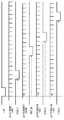
図10は、実施例1のモータ制御における変速例を示した図である。(i)は、1面目の倍率100%から2面目の倍率101%へと変更するための、モータ変速を示している。GBDレジスタには、CPU961によって倍率が設定されている。よって、GBDレジスタの記憶内容の変更は、回転速度の切り替えトリガに相当する。GBD信号の周期(a)は100%であり、(b)は101%である。それぞれの後続部分では、周期(a)と周期(b)とが安定して継続する。1回転1回検知信号Bは、図1に示した信号である。ちょうど6回のBD信号が検知されると、加速信号ACCまたは減速信号DECが1回送出される。   FIG. 10 is a diagram illustrating a shift example in the motor control according to the first embodiment. (I) shows the motor speed change for changing the magnification of the first surface from 100% to the magnification of the second surface of 101%. A magnification is set by the CPU 961 in the GBD register. Therefore, the change in the contents stored in the GBD register corresponds to a rotation speed switching trigger. The period (a) of the GBD signal is 100%, and (b) is 101%. In each subsequent portion, the period (a) and the period (b) continue stably. The one rotation detection signal B is the signal shown in FIG. When exactly six BD signals are detected, the acceleration signal ACC or the deceleration signal DEC is sent once.

GBD信号の変動を受けて、周期計測部192は計測を行う。チャネル1150xと1150yでのGBD位相関係が定義されないため、変動初期には(d)のようにGBD信号の周期が倍ほどとなってしまう。よって、回転速度が50%程度に低下してしまう場合がある。   In response to the fluctuation of the GBD signal, the period measurement unit 192 performs measurement. Since the GBD phase relationship between the channels 1150x and 1150y is not defined, the period of the GBD signal is doubled as shown in (d) at the beginning of the fluctuation. Therefore, the rotation speed may be reduced to about 50%.

本発明の逸脱判定部193は、これを検知し、逸脱判定信号EをHiに遷移させる。これにともない、平均処理部194は、リセットされ、T1が示すように、4回のカウントをやり直す。最終的に、T1は、101%(=9900XBカウント)となる。このように、平均値が所定範囲を逸脱していると判定されると、平均処理をリセットしてやり直させることで、目標速度保持部195に保持されている目標速度が維持されることになる。なお、逸脱判定信号EがLoであれば、平均処理部194は、平均化処理を継続する。すなわち、平均値が所定範囲を逸脱していないと判定されると、平均値にしたがって決定された目標速度によって、目標速度保持部195に保持されている目標速度が更新されることになる。   The departure determination unit 193 of the present invention detects this and shifts the departure determination signal E to Hi. Along with this, the average processing unit 194 is reset and starts counting four times as indicated by T1. Eventually, T1 becomes 101% (= 9900 × B count). As described above, when it is determined that the average value is out of the predetermined range, the target speed held in the target speed holding unit 195 is maintained by resetting the average process and starting over. Note that if the deviation determination signal E is Lo, the averaging processing unit 194 continues the averaging process. That is, when it is determined that the average value does not deviate from the predetermined range, the target speed held in the target speed holding unit 195 is updated with the target speed determined according to the average value.

逸脱判定信号EがHiとなったため、禁止処理回路170は、目標速度値T1に加減算される前に、位相制御量T4を強制的に0に設定する。よって、目標速度切り替え時にポリゴンミラーが目標の回転速度に対して100%付近の回転速度で回転しているにも関わらず、目標の回転速度に対して50%の回転速度で回転していると誤判断されてしまうことを抑制することができる。   Since the departure determination signal E becomes Hi, the prohibition processing circuit 170 forcibly sets the phase control amount T4 to 0 before being added to or subtracted from the target speed value T1. Therefore, when the polygon mirror is rotating at a rotation speed near 100% with respect to the target rotation speed when the target speed is switched, the polygon mirror is rotating at a rotation speed of 50% with respect to the target rotation speed. It is possible to suppress erroneous determination.

逸脱判定部193と平均処理部194の機能により、101%への目標の切り替えは、平均処理のやり直し開始部分を始点としてスムーズに終了する。これに伴い、BD制御部155は、S271で、GBD信号とBD信号の差異を小さくするよう、加速指示を送出する。これにより、DCモータドライバは、DCモータを加速させ、ポリゴンミラー802も徐々に加速する。   Due to the functions of the departure determination unit 193 and the average processing unit 194, the target switching to 101% is smoothly completed with the start of the re-starting of the average processing as a starting point. Accordingly, the BD control unit 155 sends an acceleration instruction so as to reduce the difference between the GBD signal and the BD signal in S271. Thereby, the DC motor driver accelerates the DC motor, and the polygon mirror 802 gradually accelerates.

全体としては、トリガから平均やり直し開始部分を経由し(b3)のようにスムーズに、フィードバック制御が安定する。これにより、S272で、加減速信号生成部197は、変速を終了する。   As a whole, the feedback control is stabilized smoothly from the trigger through the average redo start portion as shown in (b3). Thereby, in S272, the acceleration / deceleration signal generation unit 197 ends the shift.

図10の(b3)は目標速度値T1の変化に対してフィードバック制御が追従する様子を示した図である。この変速に要する時間(S271〜S272)は規定時間内(例:90msec)となるように設計される。   (B3) of FIG. 10 is a diagram showing how the feedback control follows the change in the target speed value T1. The time required for this speed change (S271 to S272) is designed to be within a specified time (eg, 90 msec).

なお、従来例では、GBDの周期に従ってT1が倍程度の極端な長周期に設定され、加速とは逆の、期待しない急激な減速動作が発生する。倍周期の誤検知(S231)から6面遅れで正しい101%基準が制御に反映され、制御がやり直され。その結果、変速に要する時間は、140msecほどに遅くなる。   In the conventional example, T1 is set to an extremely long cycle that is approximately double according to the GBD cycle, and an unexpected and unexpected deceleration operation occurs contrary to acceleration. The correct 101% reference is reflected in the control with a delay of 6 planes from the double cycle false detection (S231), and the control is restarted. As a result, the time required for shifting becomes as slow as 140 msec.

本実施例では、規定時間内に変速が終了する。よって、CPU961は、S270の変速開始指示から90msecにて、S280へ移行できる。   In this embodiment, the shift is completed within a specified time. Therefore, the CPU 961 can proceed to S280 after 90 msec from the shift start instruction in S270.

S280で、CPU961は、1枚目裏面(2面目)の描画開始指示をプリントコントローラおよびPWM部に送信する。これにより2面目のプリントデータについて描画が開始される。   In S280, the CPU 961 transmits a drawing start instruction for the first sheet back surface (second surface) to the print controller and the PWM unit. As a result, drawing is started for the print data on the second side.

S281で、CPU961は、2面目の描画が終了したか否かを判定する。例えば、2面目の描画開始から1990msec後に、2面目の描画が完了する。   In step S281, the CPU 961 determines whether drawing on the second surface is completed. For example, drawing of the second surface is completed after 1990 msec from the start of drawing of the second surface.

S290で、CPU961は、変速の開始を指示することで、2枚目表面(3面目)用に画像を拡大して描画をするための準備を開始する。拡大するのは、1枚目と2枚目の紙種が異なるからである。例えば、樹脂系の用紙では、加熱加圧定着処理によって紙の樹脂成分が圧延するため、用紙が伸長する。よって、3面の画像サイズを、1面目及び2面目の画像サイズと一致させるためには、倍率の拡大が必要となる。   In S290, the CPU 961 instructs to start shifting, and starts preparation for enlarging and drawing an image for the second surface (third surface). The reason for the enlargement is that the first and second paper types are different. For example, in the case of resin-based paper, the resin component of the paper is rolled by the heat and pressure fixing process, so that the paper expands. Accordingly, in order to make the image size of the third side coincide with the image size of the first side and the second side, it is necessary to enlarge the magnification.

S252で、GBD生成回路190は、3面目の設定をチャネル1150zに適用する。セレクタ140の切り替え指示に伴い、495usec(=99000XAカウント)であったGBD信号の周期は、505usec(=101000XAカウント)となる。S291で、加減速信号生成部197は、DCモータの変速を開始する。   In S252, the GBD generation circuit 190 applies the setting of the third surface to the channel 1150z. With the switching instruction of the selector 140, the period of the GBD signal that was 495 usec (= 99000 XA count) becomes 505 usec (= 101000 XA count). In S291, the acceleration / deceleration signal generation unit 197 starts shifting the DC motor.

ここで、図10(ii)を参照する。CPU961からのセレクタ140への切り替え指示がモータ変速開始のトリガとなる。(ii)は、2面目の101%から3面目の99%へのモータ変速の様子を示している。GBDの周期(b)が101%に相当し、周期(c)は99%に相当する。   Here, reference is made to FIG. A switching instruction from the CPU 961 to the selector 140 is a trigger for starting the motor shift. (Ii) shows the state of motor speed change from 101% on the second surface to 99% on the third surface. The period (b) of GBD corresponds to 101%, and the period (c) corresponds to 99%.

周期計測部192は、GBD信号の変動を検知する。変動初期には、図10(e)が示すように、GBD信号の周期が半分程度となり、回転速度が200%程度に増加してしまう場合がある。しかし、実施例1では、2面目と同じように、逸脱判定部と平均処理部194の機能により、99%への目標の切り替えがスムーズに終了する。全体としては、トリガから平均やり直し開始部分を経由し、(c3)のようにスムーズにフィードバック制御が安定する。S292で、加減速信号生成部197は変速を終了する。その後、S295に進む。本実施例では、変速時間は、90msecに収まるが、従来例では、最大で140msecほどに遅くなった。   The period measurement unit 192 detects a change in the GBD signal. At the beginning of the fluctuation, as shown in FIG. 10 (e), the period of the GBD signal may be about half and the rotation speed may increase to about 200%. However, in the first embodiment, the target switching to 99% is smoothly completed by the functions of the departure determination unit and the average processing unit 194 as in the second screen. As a whole, the feedback control is smoothly stabilized as shown in (c3) through the average redo starting portion from the trigger. In S292, the acceleration / deceleration signal generation unit 197 ends the shift. Thereafter, the process proceeds to S295. In this embodiment, the shift time is within 90 msec, but in the conventional example, it is as late as 140 msec at the maximum.

S295で、CPU961は、2枚目表面(3面目)の描画開始指示をプリントコントローラおよびPWM部に対して行う。   In step S295, the CPU 961 issues a drawing start instruction for the second surface (third surface) to the print controller and the PWM unit.

S296で、CPU961は、3面目の描画が終了したか否かを判定する。例えば、3枚目の描画開始から2010msec後に3面目の描画が完了する。   In S296, the CPU 961 determines whether drawing on the third surface is completed. For example, the drawing on the third surface is completed after 2010 msec from the start of drawing the third sheet.

S297で、CPU961は、プリント終了シーケンスを実行する。例えば、CPU961は、現像高圧バイアスの印加の解除を高圧電源部に指示する。また、CPU961は、感光ドラム708の回転を停止させる。さらに、CPU961は、ポリゴンモータ制御部に状態0への遷移を指示する。S298で、ポリゴンモータ制御部は、状態6に遷移する。その後、S299で、状態0へと遷移する。これに伴い、APCもレーザ消灯状態となる。これにより、終了シーケンスが完了する。   In S297, the CPU 961 executes a print end sequence. For example, the CPU 961 instructs the high voltage power supply unit to cancel the application of the development high voltage bias. Further, the CPU 961 stops the rotation of the photosensitive drum 708. Further, the CPU 961 instructs the polygon motor control unit to transition to the state 0. In S298, the polygon motor control unit transits to state 6. Thereafter, in S299, the state transits to state 0. As a result, the APC is also turned off. This completes the end sequence.

図10の(iii)は、S295からS296の区間のうち、GBD周期(c)[(f1)+(f2)=(c)]となる区間に、予期せぬGBDが増えた例を示している。(f1)(f2)のそれぞれで、GBD周期は、200%前後へ拡大し、異常周期となっている。   (Iii) of FIG. 10 shows an example in which the unexpected GBD has increased in a section where the GBD cycle (c) [(f1) + (f2) = (c)] in the section from S295 to S296. Yes. In each of (f1) and (f2), the GBD period is expanded to around 200%, which is an abnormal period.

逸脱判定部193は異常周期を検知すると、逸脱判定信号Eを続けてHiに遷移させる。これに伴い、平均処理部194はリセットされる。図10のT1が示すように、平均処理部における4カウントをやり直す、禁止処理回路170が、即時に、位相調整量を0に強制する。よって、速度検知異常と位相差異常による応答が全てキャンセルされる。なお、従来例では、GBD周期(f1)、(f2)に従って描画中に異常速度が発生するので、画像不良が発生する。   When the departure determination unit 193 detects the abnormal period, the departure determination unit E 193 continues to shift the departure determination signal E to Hi. Accordingly, the average processing unit 194 is reset. As indicated by T1 in FIG. 10, the prohibition processing circuit 170 that redoes 4 counts in the average processing unit immediately forces the phase adjustment amount to zero. Therefore, all responses due to speed detection abnormality and phase difference abnormality are cancelled. In the conventional example, since an abnormal speed is generated during drawing according to the GBD periods (f1) and (f2), an image defect occurs.

本実施例によれば、GBD生成回路190が高速のクロックXAにしたがって回転基準信号を生成することで回転多面鏡における回転速度の微調整幅の高分解能化を達成できる。一方で、加減速信号生成部197は低速のクロックXBにしたがって動作するため、回路の規模の簡略化を達成できる。   According to the present embodiment, the GBD generation circuit 190 generates the rotation reference signal according to the high-speed clock XA, so that the fine adjustment width of the rotation speed in the rotary polygon mirror can be increased. On the other hand, since the acceleration / deceleration signal generation unit 197 operates according to the low-speed clock XB, the circuit scale can be simplified.

さらに、回転基準信号の周期が所定範囲を逸脱したときには回転多面鏡の回転速度の目標速度を更新しないように制御することで、2種類のクロックが併設されることの弊害を低減できる。すなわち、GBD信号の送信側と受信側とが異なるクロックを使用すると、両者の非同期動作によって信号が不安定となる。その結果、制御精度が低下したり、電気的な外乱ノイズに対する耐性が低下したりして、形成される画像の品質も低下してしまう。本実施例では、GBD信号の周期にもとづいてGBD信号の信頼性を判断し、信頼性が高ければ受信したGBD信号に基づいて目標速度を更新し、信頼性が低ければ更新を抑制する。これにより、2種類のクロックが併設されることの弊害を低減できる。   In addition, when the cycle of the rotation reference signal deviates from the predetermined range, it is possible to reduce the adverse effect of providing two types of clocks by controlling so as not to update the target speed of the rotary polygon mirror. That is, when different clocks are used on the transmitting side and the receiving side of the GBD signal, the signal becomes unstable due to the asynchronous operation of both. As a result, the control accuracy is lowered, the resistance to electrical disturbance noise is lowered, and the quality of the formed image is also lowered. In the present embodiment, the reliability of the GBD signal is determined based on the period of the GBD signal, the target speed is updated based on the received GBD signal if the reliability is high, and the update is suppressed if the reliability is low. As a result, it is possible to reduce the adverse effects of providing two types of clocks.

また、本実施例では、回転状態信号と回転基準信号との位相差に基づいて回転位相の制御量を決定するが、回転基準信号の周期が所定範囲を逸脱したときには、位相差が制御量に反映されないようにする。これにより、信頼性の低い位相差に基づいて制御量が決定されてしまうことを抑制できる。すなわち、誤った制御に起因して発生する画質の低下を抑制できる。   In this embodiment, the control amount of the rotation phase is determined based on the phase difference between the rotation state signal and the rotation reference signal. However, when the rotation reference signal period deviates from a predetermined range, the phase difference becomes the control amount. Do not reflect. Thereby, it can suppress that control amount is determined based on a phase difference with low reliability. That is, it is possible to suppress deterioration in image quality caused by erroneous control.

また、測定した複数の周期の平均値を使用する実施例では、平均値が所定範囲を逸脱していると、平均処理をリセットしてやり直させることで、前回決定された目標速度を維持している。よって、信頼性の低い平均値に基づいた制御を抑制し、画質の低下を緩和できる。   In the embodiment using the average value of a plurality of measured periods, when the average value is out of the predetermined range, the previously determined target speed is maintained by resetting the average process and starting over. . Therefore, the control based on the average value with low reliability can be suppressed, and the deterioration of the image quality can be alleviated.

また、副走査倍率の微調整範囲に対応して所定範囲を決定している。連続した画像形成処理中に画像の副走査倍率は微調整されることがある。例えば、両面画像形成では、1面目と2面目とでは用紙の伸縮が発生する。よって、この伸縮量に応じて副走査倍率を変えないと、1面目と2面目の画像のサイズが異なってしまう。両面画像形成だけでなく、多数枚の用紙に連続して画像を形成する場合も、徐々に画像のサイズが異なってしまうことがある。よって、副走査倍率を微調整する必要がある。また、回転基準信号の周期と副走査倍率には密接な関係がある。そこで、副走査倍率の微調整範囲に対応して所定範囲を決定することが望ましい。なお、所定範囲を画像の生産性能(単位時間あたりの画像形成枚数)としてもよい。さらに、低速クロックXBに基づいて動作するカウンタの時間単位で所定範囲を表現すると、回路構成を簡略化できるであろう。   In addition, a predetermined range is determined corresponding to the fine adjustment range of the sub-scanning magnification. The image sub-scanning magnification may be finely adjusted during successive image forming processes. For example, in double-sided image formation, expansion and contraction of paper occurs on the first and second sides. Therefore, if the sub-scanning magnification is not changed according to the expansion / contraction amount, the sizes of the images on the first side and the second side will be different. Not only double-sided image formation, but also when images are formed continuously on a large number of sheets, the image sizes may gradually differ. Therefore, it is necessary to finely adjust the sub-scanning magnification. Further, there is a close relationship between the period of the rotation reference signal and the sub-scanning magnification. Therefore, it is desirable to determine the predetermined range corresponding to the fine adjustment range of the sub-scanning magnification. The predetermined range may be the image production performance (the number of images formed per unit time). Furthermore, if the predetermined range is expressed in units of time of a counter that operates based on the low-speed clock XB, the circuit configuration can be simplified.

以上、実施例1の装置によれば、高周波クロックXAにより、微細な副走査倍率調整が可能となる。高速クロックXAにより順序回路動作を行う部分をGBD生成回路190に限定することで、加減速信号生成部197側の回路規模を小さくでき、かつ、低コストを実現できる。また、実施例1によれば、装置の仕様によって決定される回転速度の変速範囲(例:±1%)に応じて逸脱判定範囲が決定される。   As described above, according to the apparatus of the first embodiment, it is possible to finely adjust the sub-scanning magnification with the high-frequency clock XA. By limiting the part that performs the sequential circuit operation with the high-speed clock XA to the GBD generation circuit 190, the circuit scale on the acceleration / deceleration signal generation unit 197 side can be reduced and the cost can be reduced. Further, according to the first embodiment, the deviation determination range is determined according to the speed change range (for example, ± 1%) of the rotational speed determined by the specifications of the device.

Claims (5)

画像形成装置であって、
回転多面鏡と、
前記回転多面鏡を駆動する駆動手段と、
前記回転多面鏡の回転状態を検知し、該回転状態を示す回転状態信号を出力する回転状態検知手段と、
第1クロックを生成する第1クロック生成手段と、
前記回転多面鏡の回転基準となる回転基準信号を前記第1クロックにしたがって生成する回転基準信号生成手段と、
前記回転基準信号の周期よりも短く、かつ、前記第1クロックの周期よりも長い周期の第2クロックを生成する第2クロック生成手段と、
前記回転基準信号を前記第2クロックにしたがって受信する受信手段と、
前記受信手段により受信した前記回転基準信号と前記回転状態信号との位相差を前記第2クロックにしたがって測定する位相差測定手段と、
前記位相差に基づいて前記駆動手段に加速信号または減速信号を供給する制御手段と
を備えた画像形成装置。
An image forming apparatus,
A rotating polygon mirror,
Driving means for driving the rotary polygon mirror;
Rotation state detection means for detecting a rotation state of the rotary polygon mirror and outputting a rotation state signal indicating the rotation state;
First clock generating means for generating a first clock;
A rotation reference signal generating means for generating a rotation reference signal as a rotation reference of the rotary polygon mirror according to the first clock;
Second clock generation means for generating a second clock having a cycle shorter than the cycle of the rotation reference signal and longer than the cycle of the first clock;
Receiving means for receiving the rotation reference signal according to the second clock;
Phase difference measuring means for measuring a phase difference between the rotation reference signal received by the receiving means and the rotation state signal according to the second clock;
An image forming apparatus comprising: a control unit that supplies an acceleration signal or a deceleration signal to the driving unit based on the phase difference.
前記回転基準信号の周期を前記第2クロックにしたがって測定する周期測定手段と、
前記周期に応じて前記回転多面鏡の回転速度の目標速度を決定する目標速度決定手段と、
前記目標速度を保持する保持手段と、
前記周期が所定範囲内であるかそれとも該所定範囲を逸脱しているかを判定する判定手段と、
前記周期が前記所定範囲を逸脱していると判定されると、前記保持手段に保持されている目標速度の変更を抑制する抑制手段と
を備えたことを特徴とする請求項1に記載の画像形成装置。
Period measuring means for measuring the period of the rotation reference signal according to the second clock;
Target speed determining means for determining a target speed of the rotational speed of the rotary polygon mirror according to the period;
Holding means for holding the target speed;
Determining means for determining whether the period is within a predetermined range or deviates from the predetermined range;
2. The image according to claim 1, further comprising: a suppression unit that suppresses a change in the target speed held in the holding unit when it is determined that the cycle deviates from the predetermined range. Forming equipment.
前記位相差に基づいて前記回転多面鏡の回転位相の制御量を決定する制御量決定手段をさらに備え、
前記抑制手段は、前記周期が前記所定範囲を逸脱していると判定されると、前記位相差が前記制御量に反映されることを抑制することを特徴とする請求項2に記載の画像形成装置。
Further comprising a control amount determining means for determining a control amount of the rotational phase of the rotary polygon mirror based on the phase difference;
3. The image formation according to claim 2, wherein when the period is determined to deviate from the predetermined range, the suppression unit suppresses the phase difference from being reflected in the control amount. apparatus.
前記周期測定手段が測定した複数の周期の平均値を決定して、該平均値を前記判定手段に供給する平均値決定手段と、
前記抑制手段は、
前記平均値が前記所定範囲を逸脱していると前記判定手段により判定されると、前記平均値決定手段における平均処理をリセットしてやり直させることで、前記保持手段に保持されている目標速度を維持させ、
前記平均値が前記所定範囲を逸脱していないと前記判定手段により判定されると、前記平均値にしたがって前記目標速度決定手段が決定した目標速度によって前記保持手段に保持されている目標速度を更新することを特徴とする請求項2または3に記載の画像形成装置。
Determining an average value of a plurality of periods measured by the period measurement means, and supplying the average value to the determination means;
The suppression means is
When the determination means determines that the average value is out of the predetermined range, the average speed in the average value determination means is reset and restarted to maintain the target speed held in the holding means. Let
When the determination means determines that the average value does not deviate from the predetermined range, the target speed held in the holding means is updated with the target speed determined by the target speed determination means according to the average value. The image forming apparatus according to claim 2, wherein the image forming apparatus is an image forming apparatus.
前記所定範囲は、副走査倍率の微調整範囲に対応して決定された範囲であることを特徴とする請求項2ないし4のいずれか1項に記載の画像形成装置。   The image forming apparatus according to claim 2, wherein the predetermined range is a range determined corresponding to a fine adjustment range of the sub-scanning magnification.
JP2009180054A 2009-07-31 2009-07-31 Image forming apparatus Active JP5451237B2 (en)

Priority Applications (1)

Application Number Priority Date Filing Date Title
JP2009180054A JP5451237B2 (en) 2009-07-31 2009-07-31 Image forming apparatus

Applications Claiming Priority (1)

Application Number Priority Date Filing Date Title
JP2009180054A JP5451237B2 (en) 2009-07-31 2009-07-31 Image forming apparatus

Publications (2)

Publication Number Publication Date
JP2011033833A JP2011033833A (en) 2011-02-17
JP5451237B2 true JP5451237B2 (en) 2014-03-26

Family

ID=43762968

Family Applications (1)

Application Number Title Priority Date Filing Date
JP2009180054A Active JP5451237B2 (en) 2009-07-31 2009-07-31 Image forming apparatus

Country Status (1)

Country Link
JP (1) JP5451237B2 (en)

Families Citing this family (1)

* Cited by examiner, † Cited by third party
Publication number Priority date Publication date Assignee Title
JP6935288B2 (en) * 2017-09-29 2021-09-15 キヤノン株式会社 Image forming device

Also Published As

Publication number Publication date
JP2011033833A (en) 2011-02-17

Similar Documents

Publication Publication Date Title
JP2854366B2 (en) Laser scanning type image forming apparatus
JP2001180043A (en) Image forming device
US20080084571A1 (en) Image forming apparatus
JP2005198006A (en) Pixel clock and pulse modulation signal generation apparatus, optical scanning apparatus, and image forming apparatus
JP6702768B2 (en) Image forming device
JP2001174728A (en) Lighting control method for light source, and image forming device
JP5451237B2 (en) Image forming apparatus
JP2015114491A (en) Optical scanner and image forming apparatus using the same
US6236415B1 (en) Image forming apparatus and control method therefor
JP4850639B2 (en) Motor control device, motor control method, and electrophotographic image forming apparatus
JP4424230B2 (en) Image forming apparatus
JP4827341B2 (en) Motor rotation control device and image forming apparatus
JP2016212243A (en) Image formation optical scan device, image formation apparatus and image formation apparatus optical scan program
JP4866057B2 (en) Optical device, image forming apparatus, and lighting position changing method
JP2004126228A (en) Multi-beam type image forming apparatus, and multi-beam control apparatus and method
JP2006201606A (en) Light beam scanning apparatus and image forming apparatus
JP3596970B2 (en) Light beam scanning device
JP2002283616A (en) Image forming apparatus and laser diode control method for image forming apparatus
JP4599556B2 (en) Optical apparatus and image forming apparatus
JP4367840B2 (en) Pixel clock generation device, optical scanning device, and image forming device
JP2007185787A (en) Image forming apparatus
JP2006235178A (en) Image forming apparatus
JPH11237567A (en) Multi-color image formation device and method therefor
JP2005225158A (en) Image forming apparatus
JP2007112053A (en) Color image forming apparatus and its control method

Legal Events

Date Code Title Description
A621 Written request for application examination

Free format text: JAPANESE INTERMEDIATE CODE: A621

Effective date: 20120726

A977 Report on retrieval

Free format text: JAPANESE INTERMEDIATE CODE: A971007

Effective date: 20130213

TRDD Decision of grant or rejection written
A01 Written decision to grant a patent or to grant a registration (utility model)

Free format text: JAPANESE INTERMEDIATE CODE: A01

Effective date: 20131202

A61 First payment of annual fees (during grant procedure)

Free format text: JAPANESE INTERMEDIATE CODE: A61

Effective date: 20131226

R151 Written notification of patent or utility model registration

Ref document number: 5451237

Country of ref document: JP

Free format text: JAPANESE INTERMEDIATE CODE: R151