JP5437253B2 - Fabrication of red and white nitride based LEDs without phosphors - Google Patents
Fabrication of red and white nitride based LEDs without phosphors Download PDFInfo
- Publication number
- JP5437253B2 JP5437253B2 JP2010528843A JP2010528843A JP5437253B2 JP 5437253 B2 JP5437253 B2 JP 5437253B2 JP 2010528843 A JP2010528843 A JP 2010528843A JP 2010528843 A JP2010528843 A JP 2010528843A JP 5437253 B2 JP5437253 B2 JP 5437253B2
- Authority
- JP
- Japan
- Prior art keywords
- layer
- mqw
- light emitting
- red
- yellow
- Prior art date
- Legal status (The legal status is an assumption and is not a legal conclusion. Google has not performed a legal analysis and makes no representation as to the accuracy of the status listed.)
- Expired - Fee Related
Links
Images


Classifications
-
- H—ELECTRICITY
- H01—ELECTRIC ELEMENTS
- H01L—SEMICONDUCTOR DEVICES NOT COVERED BY CLASS H10
- H01L33/00—Semiconductor devices with at least one potential-jump barrier or surface barrier specially adapted for light emission; Processes or apparatus specially adapted for the manufacture or treatment thereof or of parts thereof; Details thereof
- H01L33/02—Semiconductor devices with at least one potential-jump barrier or surface barrier specially adapted for light emission; Processes or apparatus specially adapted for the manufacture or treatment thereof or of parts thereof; Details thereof characterised by the semiconductor bodies
- H01L33/04—Semiconductor devices with at least one potential-jump barrier or surface barrier specially adapted for light emission; Processes or apparatus specially adapted for the manufacture or treatment thereof or of parts thereof; Details thereof characterised by the semiconductor bodies with a quantum effect structure or superlattice, e.g. tunnel junction
- H01L33/06—Semiconductor devices with at least one potential-jump barrier or surface barrier specially adapted for light emission; Processes or apparatus specially adapted for the manufacture or treatment thereof or of parts thereof; Details thereof characterised by the semiconductor bodies with a quantum effect structure or superlattice, e.g. tunnel junction within the light emitting region, e.g. quantum confinement structure or tunnel barrier
-
- H—ELECTRICITY
- H01—ELECTRIC ELEMENTS
- H01L—SEMICONDUCTOR DEVICES NOT COVERED BY CLASS H10
- H01L27/00—Devices consisting of a plurality of semiconductor or other solid-state components formed in or on a common substrate
- H01L27/15—Devices consisting of a plurality of semiconductor or other solid-state components formed in or on a common substrate including semiconductor components with at least one potential-jump barrier or surface barrier specially adapted for light emission
- H01L27/153—Devices consisting of a plurality of semiconductor or other solid-state components formed in or on a common substrate including semiconductor components with at least one potential-jump barrier or surface barrier specially adapted for light emission in a repetitive configuration, e.g. LED bars
-
- H—ELECTRICITY
- H01—ELECTRIC ELEMENTS
- H01L—SEMICONDUCTOR DEVICES NOT COVERED BY CLASS H10
- H01L33/00—Semiconductor devices with at least one potential-jump barrier or surface barrier specially adapted for light emission; Processes or apparatus specially adapted for the manufacture or treatment thereof or of parts thereof; Details thereof
- H01L33/02—Semiconductor devices with at least one potential-jump barrier or surface barrier specially adapted for light emission; Processes or apparatus specially adapted for the manufacture or treatment thereof or of parts thereof; Details thereof characterised by the semiconductor bodies
- H01L33/08—Semiconductor devices with at least one potential-jump barrier or surface barrier specially adapted for light emission; Processes or apparatus specially adapted for the manufacture or treatment thereof or of parts thereof; Details thereof characterised by the semiconductor bodies with a plurality of light emitting regions, e.g. laterally discontinuous light emitting layer or photoluminescent region integrated within the semiconductor body
-
- H—ELECTRICITY
- H01—ELECTRIC ELEMENTS
- H01L—SEMICONDUCTOR DEVICES NOT COVERED BY CLASS H10
- H01L33/00—Semiconductor devices with at least one potential-jump barrier or surface barrier specially adapted for light emission; Processes or apparatus specially adapted for the manufacture or treatment thereof or of parts thereof; Details thereof
- H01L33/02—Semiconductor devices with at least one potential-jump barrier or surface barrier specially adapted for light emission; Processes or apparatus specially adapted for the manufacture or treatment thereof or of parts thereof; Details thereof characterised by the semiconductor bodies
- H01L33/26—Materials of the light emitting region
- H01L33/30—Materials of the light emitting region containing only elements of group III and group V of the periodic system
- H01L33/32—Materials of the light emitting region containing only elements of group III and group V of the periodic system containing nitrogen
Description
本発明は、一般に発光ダイオードのための多重量子井戸構造、及び発光ダイオードのための多重量子井戸構造を作製する方法に関する。 The present invention relates generally to a multiple quantum well structure for a light emitting diode and a method of making a multiple quantum well structure for a light emitting diode.
発光ダイオード(LED)は照明源として機能することができ、通常、屋外フルカラーディスプレイ、交通信号灯、データストレージ、固体照明及び通信などの用途に使用される。通常、III族窒化物ベースのLEDは、窒化インジウムガリウム/窒化ガリウム(InGaN/GaN)多重量子井戸(MQW)層のバンドギャップに対応する波長の光を発光する。GaN層のp−n接合部の両端にバイアスが印加されると光が発生する。LEDでは、p型及びn−GaN層により注入された正孔と電子とが活性層で結合してLED表面から光を発光する。 Light emitting diodes (LEDs) can function as illumination sources and are typically used for applications such as outdoor full color displays, traffic lights, data storage, solid state lighting and communications. Typically, Group III nitride based LEDs emit light of a wavelength corresponding to the band gap of the indium gallium nitride / gallium nitride (InGaN / GaN) multiple quantum well (MQW) layer. Light is generated when a bias is applied across the pn junction of the GaN layer. In the LED, holes and electrons injected by the p-type and n-GaN layers are combined in the active layer to emit light from the LED surface.
例えば、緑色又は黄色LEDなどの長波長用途のために高In含量が取り入れられたりした場合、InGaN/GaN MQWのエピタキシャル成長が実際的に困難な問題となる。さらに、高In取り入れで波長を増加させた発光では、通常、光出力効率が低下する。成長温度を低下させることによりInの取入れ量を増やすことはできるが、通常、低い温度では結晶品質が劣化するのでフォトルミネセンス(PL)強度が低下する。 For example, when a high In content is incorporated for long wavelength applications such as green or yellow LEDs, epitaxial growth of InGaN / GaN MQW becomes a practically difficult problem. In addition, light emission efficiency is usually lowered in light emission in which the wavelength is increased by incorporating high In. Although the amount of In taken in can be increased by lowering the growth temperature, usually the crystal quality deteriorates at a lower temperature, so that the photoluminescence (PL) intensity is lowered.
LEDの量子効率を高めるために、InGaN量子ドットが研究されてきた(CHOI他による国際公開第2004/054006号A1などを参照)。LEDからの発光色は、量子ドットの寸法を制御することにより青色から橙色に調節することができる(Grandjean他による米国特許第6,445,009号B1などを参照)。DenBaars他は、米国特許出願第2006/0255347号A1に、GaNを1又はそれ以上の希土類遷移元素でドープして様々な色合いを有する調節可能なLEDを得ることを記載している。これらの遷移元素はCr、Ti及びCoを含み、これらの元素の組み合わせを使用して白色光を生成できることが提案されている。しかしながら、MQW構造の薄い活性層内への注入の深さを制御することは実際的に困難である。 InGaN quantum dots have been studied to increase the quantum efficiency of LEDs (see, eg, WO 2004/054006 A1 by CHOI et al.). The color emitted from the LED can be adjusted from blue to orange by controlling the size of the quantum dots (see, for example, US Pat. No. 6,445,009 B1 by Grandjean et al.). DenBaars et al. In US Patent Application No. 2006/0255347 A1 describes doping GaN with one or more rare earth transition elements to obtain tunable LEDs having various shades. These transition elements include Cr, Ti, and Co, and it has been proposed that white light can be generated using a combination of these elements. However, it is practically difficult to control the depth of implantation into the thin active layer of the MQW structure.
Chua他は、米国特許出願第2004/0023427号A1において、LEDのMQW構造の井戸層内に取り入れたInGaN量子ドットを使用した白色発光について記載している。しかしながら、p−ドーパントマグネシウム(Mg)を活性化させるために高温の原位置アニーリングを行った際に、量子ドットの井戸層内又は障壁層内への外部拡散が生じた。通常、これによりMQW層が不明確となる。この結果、量子ドットによる閉じ込め効果が危うくなる可能性がある。さらに、米国特許出願第2004/0023427号A1では、LEDからの発光色を正確に制御することができず、LEDの白色度が変動するようになっている。 Chua et al., In U.S. Patent Application No. 2004/0023427 A1, describe white light emission using InGaN quantum dots incorporated in the well layer of the MQW structure of the LED. However, when high temperature in-situ annealing was performed to activate the p-dopant magnesium (Mg), external diffusion of quantum dots into the well layer or barrier layer occurred. This usually makes the MQW layer unclear. As a result, the confinement effect by the quantum dots may be compromised. Furthermore, in US Patent Application No. 2004/0023427 A1, the color of light emitted from the LED cannot be accurately controlled, and the whiteness of the LED varies.
現在のところ、可視赤色−橙色光源及び黄色光源は、通常リン酸アルミニウムインジウムガリウム(AlInGaP)材料に基づいて得られるのに対し、明緑色、青色及び紫色LEDは、通常GaNベースの材料系から作製される。しかしながら、現在の技術では、GaNベースのLEDが、通常、白色発光を生成するための赤色成分を提供するのに必要な赤色発光を有することは知られていない。 At present, visible red-orange light sources and yellow light sources are usually obtained based on aluminum indium gallium phosphate (AlInGaP) materials, whereas light green, blue and purple LEDs are usually made from GaN-based material systems Is done. However, with current technology, it is not known that GaN-based LEDs typically have the red emission necessary to provide a red component to produce white emission.
通常、LEDから白色光を生成するためには、各々が赤色、緑色及び青色光という個々の色を発光する別個のLEDの組み合わせが使用される。或いは、個々の青色及び黄色LEDを組み合わせて白色光を生成する。1つの不利な点は、白色光を生成するために異なる材料からなる複数のLEDが使用され、これが作製技術の複雑さ及び全体の作製コストを増加させる点である。異なるダイオードの種類は異なる印加電圧を使用するので、結果として得られるデバイスは、通常複雑な制御電子回路を使用する。さらに、例えば(赤色発光用の)AlInGaP及び(緑色及び青色発光用の)InGaNなどの使用する材料の異なる劣化速度が、通常、得られる白色光の信頼性又は品質に影響を及ぼす。白色光生成のために黄色蛍光体で被覆した青色LEDを使用する代替の作製方法に関しても、蛍光体の劣化により上述の信頼性/品質の問題が生じる。また通常、蛍光体の使用は製造コストを増加させるとともに、蛍光体における吸収に起因して外部量子効率を低下させる。 Usually, to generate white light from an LED, a combination of separate LEDs, each emitting a separate color, red, green and blue light, is used. Alternatively, individual blue and yellow LEDs are combined to produce white light. One disadvantage is that multiple LEDs of different materials are used to generate white light, which increases the complexity of the fabrication technology and the overall fabrication cost. Since different diode types use different applied voltages, the resulting device typically uses complex control electronics. Furthermore, different degradation rates of the materials used, such as AlInGaP (for red emission) and InGaN (for green and blue emission) usually affect the reliability or quality of the resulting white light. With regard to an alternative fabrication method that uses a blue LED coated with a yellow phosphor for white light generation, degradation of the phosphor causes the above-mentioned reliability / quality problems. Also, the use of phosphors usually increases manufacturing costs and reduces external quantum efficiency due to absorption in the phosphors.
従って、上述の問題点の少なくとも1つに対処するために、発光ダイオードのための多重量子井戸(MQW)構造、及び発光ダイオードのためのMQW構造を作製する方法の必要性が存在する。 Accordingly, there is a need for a multiple quantum well (MQW) structure for light emitting diodes and a method of making an MQW structure for light emitting diodes to address at least one of the above-mentioned problems.
本発明の第1の態様によれば、発光ダイオードのための多重量子井戸(MQW)構造が提供され、このMQW構造は複数の量子井戸構造を含み、個々の量子井戸構造が、バリア層と、バリア層上に形成され量子ドットナノ構造を組み込んだ井戸層とを含み、これらのバリア層及び井戸層が第1の金属窒化物ベースの材料を含み、量子井戸構造の少なくとも1つが、井戸層上に形成されたキャッピング層をさらに含み、このキャッピング層が、第1の金属窒化物ベースの材料と比較して異なる金属元素を有する第2の金属窒化物ベースの材料を含む。 According to a first aspect of the present invention, there is provided a multiple quantum well (MQW) structure for a light emitting diode, the MQW structure comprising a plurality of quantum well structures, each quantum well structure comprising: a barrier layer; And a well layer incorporating quantum dot nanostructures formed on the barrier layer, the barrier layer and the well layer including a first metal nitride-based material, wherein at least one of the quantum well structures is on the well layer Further comprising a capping layer formed, the capping layer comprising a second metal nitride based material having a different metal element compared to the first metal nitride based material.
個々の量子井戸構造は、量子ドットナノ構造の形成を促進するための、バリア層と井戸層との間に形成された湿潤層をさらに含むことができる。 Individual quantum well structures can further include a wetting layer formed between the barrier layer and the well layer to facilitate the formation of quantum dot nanostructures.
量子井戸構造の少なくとも1つは、キャッピング層上に形成された第2のキャッピング層をさらに含むことができ、上記第2のキャッピング層は、第2の金属窒化物ベースの材料と比較して異なる金属元素を有する第3の金属窒化物ベースの材料を含む。 At least one of the quantum well structures can further include a second capping layer formed on the capping layer, wherein the second capping layer is different compared to the second metal nitride based material. A third metal nitride based material having a metal element is included.
MQW構造は、複数の量子井戸構造の最も外側の構造上に形成されたp型コンタクト構造をさらに含むことができ、このp型コンタクト構造は、電子ブロッキング層と、この電子ブロッキング層上に形成されたp型金属窒化物層とを含むことができる。 The MQW structure may further include a p-type contact structure formed on the outermost structure of the plurality of quantum well structures, and the p-type contact structure is formed on the electron blocking layer and the electron blocking layer. And a p-type metal nitride layer.
p型金属窒化物層はインジウム(In)材料を含むことができる。 The p-type metal nitride layer can include an indium (In) material.
p型金属窒化物層は、約750℃〜800℃の間の温度を使用して形成することができる。 The p-type metal nitride layer can be formed using a temperature between about 750 ° C. and 800 ° C.
MQW構造は、複数の量子井戸構造の下にあるn+層に電気接触するためのn型コンタクト層をさらに含むことができる。 The MQW structure can further include an n-type contact layer for making electrical contact with the n + layer underlying the plurality of quantum well structures.
MQW構造は赤色/黄色光を発光することができる。 The MQW structure can emit red / yellow light.
MQW構造は赤色光を発光することができる。 The MQW structure can emit red light.
キャッピング層は窒化アルミニウム(AlN)材料を含むことができる。 The capping layer can include an aluminum nitride (AlN) material.
キャッピング層の厚みは最大約3nmに保持することができる。 The thickness of the capping layer can be kept up to about 3 nm.
量子ドットナノ構造は、インジウムガリウム窒化物(InGaN)量子ドットを含むことができる。 The quantum dot nanostructure can include indium gallium nitride (InGaN) quantum dots.
本発明の第2の態様によれば、発光ダイオード構造が提供され、この発光ダイオード構造は赤色/黄色発光多重量子井戸(MQW)構造を含み、赤色/黄色発光MQWの個々の量子井戸構造が、バリア層と、バリア層上に形成され量子ドットナノ構造を組み込んだ井戸層とを含み、これらのバリア層及び井戸層が第1の金属窒化物ベースの材料を含み、赤色/黄色発光MQWの量子井戸構造の少なくとも1つが、井戸層上に形成されたキャッピング層をさらに含み、このキャッピング層が、第1の金属窒化物ベースの材料と比較して異なる金属元素を有する第2の金属窒化物ベースの材料を含み、発光ダイオード構造はさらに、発光ダイオード構造から白色光を発光するために赤色/黄色発光MQWと一体に形成された青色発光MQW構造を含む。 According to a second aspect of the present invention, a light emitting diode structure is provided, the light emitting diode structure comprising a red / yellow light emitting multiple quantum well (MQW) structure, wherein the individual quantum well structures of the red / yellow light emitting MQW are: A quantum well of red / yellow light emitting MQW comprising a barrier layer and a well layer formed on the barrier layer and incorporating a quantum dot nanostructure, the barrier layer and the well layer comprising a first metal nitride based material At least one of the structures further includes a capping layer formed on the well layer, the capping layer comprising a second metal nitride based material having a different metal element as compared to the first metal nitride based material. The light emitting diode structure further includes a blue light emitting MQW structure integrally formed with the red / yellow light emitting MQW to emit white light from the light emitting diode structure. No.
青色発光MQW構造は、赤色/黄色発光MQW構造の複数の量子井戸構造の最も外側の構造上に形成することができる。 The blue light emitting MQW structure can be formed on the outermost structure of the plurality of quantum well structures of the red / yellow light emitting MQW structure.
赤色/黄色発光MQW構造の複数の量子井戸構造の最も内側の構造は、青色発光MQW構造上に形成することができる。 The innermost structure of the plurality of quantum well structures of the red / yellow light emitting MQW structure can be formed on the blue light emitting MQW structure.
発光ダイオード構造は、赤色/黄色発光及び青色発光MQW構造の下にあるn+層に電気接触するためのn型コンタクト層と、赤色/黄色発光MQW構造及び青色発光MQW構造上に形成されたそれぞれのp型コンタクト構造とをさらに含むことができ、このp型コンタクト構造は各々、電子ブロッキング層と、この電子ブロッキング層上に形成されたp型金属窒化物層とを含むことができる。 The light emitting diode structure includes an n-type contact layer for making electrical contact with the n + layer under the red / yellow light emitting and blue light emitting MQW structures, and a red / yellow light emitting MQW structure and a blue light emitting MQW structure, respectively. Each of the p-type contact structures may further include an electron blocking layer and a p-type metal nitride layer formed on the electron blocking layer.
発光ダイオード構造は、青色発光MQW構造の下にあるn+層に電気接触するためのn型コンタクト層と、青色発光MQW構造の活性化するための、青色発光MQW構造上に形成されたp型コンタクト層とをさらに含むことができ、赤色/黄色発光MQW構造は、青色発光MQW構造からの青色発光の吸収に基づいて赤色/黄色光を発光することができる。 The light emitting diode structure includes an n-type contact layer for making electrical contact with the n + layer under the blue light emitting MQW structure, and a p-type formed on the blue light emitting MQW structure for activating the blue light emitting MQW structure. A contact layer, and the red / yellow light emitting MQW structure can emit red / yellow light based on absorption of blue light emission from the blue light emitting MQW structure.
キャッピング層は窒化アルミニウム(AlN)材料を含むことができる。 The capping layer can include an aluminum nitride (AlN) material.
キャッピング層の厚みは最大約3nmに保持することができる。 The thickness of the capping layer can be kept up to about 3 nm.
量子ドットナノ構造はインジウムガリウム窒化物(InGaN)量子ドットを含むことができる。 The quantum dot nanostructure can include indium gallium nitride (InGaN) quantum dots.
本発明の第3の態様によれば、発光ダイオード構造が提供され、この発光ダイオード構造は赤色/黄色発光多重量子井戸(MQW)構造を含み、赤色/黄色発光MQWの個々の量子井戸構造が、バリア層と、バリア層上に形成され量子ドットナノ構造を組み込んだ井戸層とを含み、これらのバリア層及び井戸層が第1の金属窒化物ベースの材料を含み、赤色/黄色発光MQWの量子井戸構造の少なくとも1つが、井戸層上に形成されたキャッピング層をさらに含み、このキャッピング層が、第1の金属窒化物ベースの材料と比較して異なる金属元素を有する第2の金属窒化物ベースの材料を含み、発光ダイオード構造はさらに、青色発光MQW構造と緑色発光MQW構造とを含み、これらの青色発光MQW構造及び緑色発光MQW構造が、発光ダイオード構造から白色光を発光するために赤色/黄色発光MQWと一体に形成される。 According to a third aspect of the present invention, a light emitting diode structure is provided, the light emitting diode structure comprising a red / yellow light emitting multiple quantum well (MQW) structure, wherein the individual quantum well structures of the red / yellow light emitting MQW are: A quantum well of red / yellow light emitting MQW comprising a barrier layer and a well layer formed on the barrier layer and incorporating a quantum dot nanostructure, the barrier layer and the well layer comprising a first metal nitride based material At least one of the structures further includes a capping layer formed on the well layer, the capping layer comprising a second metal nitride based material having a different metal element as compared to the first metal nitride based material. The light emitting diode structure further includes a blue light emitting MQW structure and a green light emitting MQW structure, and the blue light emitting MQW structure and the green light emitting MQW structure are It is formed on the red / yellow light emitting MQW integral to emit white light from the diode structure.
赤色/黄色発光MQW構造は、青色発光MQW構造及び緑色発光MQW構造上に形成することができる。 The red / yellow light emitting MQW structure can be formed on the blue light emitting MQW structure and the green light emitting MQW structure.
発光ダイオード構造は、赤色/黄色発光、青色発光及び緑色発光MQW構造の下にあるn+層に電気接触するためのn型コンタクト層と、青色発光MQW構造及び緑色発光MQW構造をそれぞれ活性化するための、青色発光MQW構造及び緑色発光MQW構造上に形成されたそれぞれのp型コンタクト構造とをさらに含むことができ、このp型コンタクト構造は各々、電子ブロッキング層と、この電子ブロッキング層上に形成されたp型金属窒化物層とを含むことができ、さらに赤色/黄色発光構造は、青色発光MQW構造からの青色発光、緑色発光MQW構造からの緑色発光、又はこれらの両方の吸収に基づいて赤色/黄色光を発光することができる。 The light emitting diode structure activates an n-type contact layer for making electrical contact with the n + layer under the red / yellow light emitting, blue light emitting and green light emitting MQW structures, and a blue light emitting MQW structure and a green light emitting MQW structure, respectively. And a p-type contact structure formed on the blue light-emitting MQW structure and the green light-emitting MQW structure, respectively, wherein the p-type contact structure is formed on the electron blocking layer and the electron blocking layer, respectively. And a red / yellow light emitting structure based on absorption of blue light emission from the blue light emitting MQW structure, green light emission from the green light emitting MQW structure, or both. Can emit red / yellow light.
キャッピング層は窒化アルミニウム(AlN)材料を含むことができる。 The capping layer can include an aluminum nitride (AlN) material.
キャッピング層の厚みは最大約3nmに保持することができる。 The thickness of the capping layer can be kept up to about 3 nm.
量子ドットナノ構造はインジウムガリウム窒化物(InGaN)量子ドットを含むことができる。 The quantum dot nanostructure can include indium gallium nitride (InGaN) quantum dots.
本発明の第4の態様によれば、発光ダイオードのための多重量子井戸(MQW)構造を作製する方法が提供され、この方法は、各々がバリア層と、バリア層上に形成され量子ドットナノ構造を組み込んだ井戸層とを含み、これらのバリア及び井戸層が第1の金属窒化物ベースの材料を含む複数の量子井戸構造を形成するステップと、第1の金属窒化物ベースの材料と比較して異なる金属元素を有する第2の金属窒化物ベースの材料を含むキャッピング層を井戸層上にさらに含むように量子井戸構造の少なくとも1つを形成するステップとを含む。 According to a fourth aspect of the present invention, there is provided a method of making a multiple quantum well (MQW) structure for a light emitting diode, the method comprising a barrier layer and a quantum dot nanostructure each formed on the barrier layer. Forming a plurality of quantum well structures, wherein the barrier and well layers include a first metal nitride based material, and comparing the first metal nitride based material to the first metal nitride based material. Forming at least one of the quantum well structures to further include a capping layer on the well layer including a second metal nitride-based material having different metal elements.
本発明の第5の態様によれば、発光ダイオード構造を作製する方法が提供され、この方法は、各々がバリア層と、バリア層上に形成され量子ドットナノ構造を組み込んだ井戸層とを含み、これらのバリア及び井戸層が第1の金属窒化物ベースの材料を含む複数の量子井戸構造を形成するステップと、第1の金属窒化物ベースの材料と比較して異なる金属元素を有する第2の金属窒化物ベースの材料を含むキャッピング層を井戸層上にさらに含むように赤色/黄色MQWの量子井戸構造の少なくとも1つを形成するステップと、発光ダイオード構造から白色光を発光するために赤色/黄色発光MQWと一体に青色発光MQW構造を形成するステップとを含む。 According to a fifth aspect of the present invention, there is provided a method of making a light emitting diode structure, the method comprising a barrier layer and a well layer each formed on the barrier layer and incorporating a quantum dot nanostructure, Forming a plurality of quantum well structures in which the barrier and well layers include a first metal nitride-based material, and a second metal element having a different metal element compared to the first metal nitride-based material. Forming at least one of a red / yellow MQW quantum well structure to further include a capping layer comprising a metal nitride-based material on the well layer; and red / yellow to emit white light from the light emitting diode structure. Forming a blue light emitting MQW structure integrally with the yellow light emitting MQW.
本発明の第6の態様によれば、発光ダイオード構造を作製する方法が提供され、この方法は、各々がバリア層と、バリア層上に形成され量子ドットナノ構造を組み込んだ井戸層とを含み、これらのバリア及び井戸層が第1の金属窒化物ベースの材料を含む複数の量子井戸構造を形成するステップと、第1の金属窒化物ベースの材料と比較して異なる金属元素を有する第2の金属窒化物ベースの材料を含むキャッピング層を井戸層上にさらに含むように赤色/黄色MQWの量子井戸構造の少なくとも1つを形成するステップと、青色発光MQW構造を赤色/黄色発光MQWと一体に形成するステップと、発光ダイオード構造から白色光を発光するために赤色/黄色発光MQW及び青色発光MQW構造と一体に緑色発光MQW構造を形成するステップとを含む。 According to a sixth aspect of the present invention, there is provided a method of making a light emitting diode structure, the method comprising a barrier layer and a well layer each formed on the barrier layer and incorporating a quantum dot nanostructure, Forming a plurality of quantum well structures in which the barrier and well layers include a first metal nitride-based material, and a second metal element having a different metal element compared to the first metal nitride-based material. Forming at least one of a red / yellow MQW quantum well structure to further include a capping layer including a metal nitride-based material on the well layer; and integrating the blue light emitting MQW structure with the red / yellow light emitting MQW. Forming a green light emitting MQW structure integrally with the red / yellow light emitting MQW structure and the blue light emitting MQW structure in order to emit white light from the light emitting diode structure. And a flop.
当業者には、例示のみの目的で図面とともに示す以下の説明から、本発明の実施形態がより良く理解されるとともに容易に明らかになるであろう。 For those skilled in the art, embodiments of the present invention will be better understood and readily apparent from the following description, taken in conjunction with the drawings for illustrative purposes only.
説明する実施形態例では、有機金属化学気相成長(MOCVD)装置を使用してLEDの成長が行われる。実施形態例では、トリメチルガリウム(TMGa)、トリメチルインジウム(TMIn)、トリメチルアルミニウム(TMA)、マグネシウム(Cp2Mg)及びシラン(SiH4)が前駆体として使用される。LED表面上で元素を効果的に取り込むための搬送ガスとして水素及び窒素が使用される。 In the described example embodiment, the growth of the LED is performed using a metal organic chemical vapor deposition (MOCVD) apparatus. In the example embodiment, trimethylgallium (TMGa), trimethylindium (TMIn), trimethylaluminum (TMA), magnesium (Cp 2 Mg) and silane (SiH 4 ) are used as precursors. Hydrogen and nitrogen are used as carrier gases for effectively capturing elements on the LED surface.
実施形態例では、多重量子井戸(MQW)構造が、InGaN井戸層上におけるInGaN量子ドットの取入れとともに規定の温度で成長する。その後、形成された量子井戸が薄い窒化アルミニウム(AlN)層でキャッピングされる。以下、この実施形態例について詳述する。 In an example embodiment, a multiple quantum well (MQW) structure is grown at a defined temperature with the incorporation of InGaN quantum dots on the InGaN well layer. The formed quantum well is then capped with a thin aluminum nitride (AlN) layer. Hereinafter, this embodiment will be described in detail.
AlN層は、InGaN量子ドットの外部拡散を防ぐためのキャップ層として機能することができる。InXGa1-XN又はInN量子ドットの格子定数が約3.5446オングストローム(Å)であるのに対し、AlN層の格子定数は約3.1114(Å)である。これにより、GaN/InN系(約10.6%)と比較した場合、AlN/InN系(約13%)ではより大きな格子不整合が生じる。このより大きな格子不整合が、その後の層成長及びアニーリング処理中に高温が印加された場合の量子ドットの外部拡散をさらに阻止することができる。AlN層は、その後のInGaN井戸の成長に対してより大きな圧縮応力を発生させる可能性があるので、本発明者らは、GaNバリアの成長後かつInGaN量子ドット及びInGaN井戸層の成長前の中間層としてAlN層を使用することは推奨しない。この結果、インジウムの取入れ及びその発光波長の青色シフトが弱まる可能性がある。 The AlN layer can function as a cap layer for preventing external diffusion of InGaN quantum dots. The lattice constant of In X Ga 1-X N or InN quantum dots is about 3.5446 angstrom (Å), whereas the lattice constant of the AlN layer is about 3.1114 (Å). Thereby, when compared with the GaN / InN system (about 10.6%), a larger lattice mismatch occurs in the AlN / InN system (about 13%). This larger lattice mismatch can further prevent outdiffusion of quantum dots when high temperatures are applied during subsequent layer growth and annealing processes. Since the AlN layer may generate a greater compressive stress for subsequent growth of the InGaN wells, we have intervened after the growth of the GaN barrier and before the growth of the InGaN quantum dots and InGaN well layers. It is not recommended to use an AlN layer as the layer. As a result, the uptake of indium and the blue shift of its emission wavelength can be weakened.
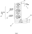
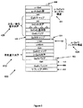
図1は、この実施形態例の単色LED構造100を示す概略図である。処理チャンバ内にサファイア基板102が準備される。サファイア基板102上のGaNの核生成を促進するために、基板102上で低温バッファ層106を約520℃〜550℃の温度範囲で約26nmの厚みに成長させる。1018cm-3のドーピング濃度のGaNのn+層108を、層106上で約900℃〜1050℃の温度で成長させる。層108が成長した後、GaNバリア層110を、約2×1017cm-3〜1×1018cm-3のSiドーピング濃度で約5〜15nmの厚みに成長させる。当業者であれば、バリア層110をSiドーピングなしで成長させることはできるが、通常バリア層110の品質はSiドーピングで向上するので、Siドーピングが好ましいと思われる点を理解するであろう。
FIG. 1 is a schematic diagram illustrating a
バリア層110が成長した後、温度が約700〜750℃に下げられ、x〜0.10−0.20の組成及び約1nmの厚みを有するInXGa1-XNの薄い湿潤層112をバリア層110上で成長させる。湿潤層112は、Inバースト処理中の窒化インジウムリッチな量子ドットの取入れを促進することができる。薄い湿潤層112を形成した後、インジウム前駆体TMInが、基板102を越えて約20μモル/分未満の流速で約6〜30秒間流れて、0.2<w<1.0とした場合InWGa1-WNの114などのナノ構造又は「量子ドット」を形成する。インジウム前駆体TMInからのIn原子は、InGaNの湿潤層の窒素ダングリングボンドにおいて分離して、前駆体の流速により決定される114などのInGaN量子ドット成長のためのシード層として機能することができる。114などのインジウムリッチなInGaN量子ドットのサイズを制御するために、アンチサーファクタントとしての機能を果たすTMInフローの量及びTMInフローの持続時間がモニタされる。TMInの流速が約20μモル/分未満に、好ましくは約20sccm(4.5μモル/分)〜約80sccm(18.0μモル/分)に保持されて、114などのInリッチなInGaN量子ドットを形成する。
After the
114などの量子ドットが成長した後、114などのナノ構造上でInGaN量子井戸層116を成長させ、約3〜5nmの厚みの組み込まれたInGaN量子ドット/井戸層116を形成する。0.2<w<0.5のインジウム組成をもたらすために、InWGa1-WN井戸層116の成長温度は約700℃〜750℃に保持される。インジウムの取入れ量は所望の発光色に依存する。単色発光を得るために、MQWの成長中、114などの量子ドット及び井戸層116の成長中などは温度変動が最小限に抑えられる。井戸層116が成長した後、井戸層116はAlN層118でキャッピングされる。AlN層118の厚みは、井戸層116と比較して(好ましくは約3nmよりも薄く)相対的に薄く保たれる。この実施形態例では、InGaN井戸層116の成長後、AlN層118を成長させる前に約30秒を越える時間間隔が保持される。より良好な結晶品質のために、AlN層118及びGaNバリア層110を成長させるための温度は、InGaN井戸層116を成長させるための温度よりも約0〜30℃高く設定することができる。AlN層118が成長した後、GaN層108を成長させるための条件と実質的に同じ条件を使用してGaNキャップ層120を成長させる。
After a quantum dot such as 114 is grown, an InGaN
バリア層110からGaNキャップ層120までが、赤色/黄色発光量子井戸構造122を形成する。この実施形態例では、バリア層110からGaNキャップ層120までを形成するステップを繰り返して(量子井戸構造124などを参照)赤色/黄色発光多重量子井戸(MQW)構造126を形成する。
The
当業者であれば、説明を明確にするために図1には2つの量子井戸構造122、124のみを示しているが、量子井戸構造の数は3〜5などの範囲に及んでもよいことを理解するであろう。当業者であれば理解するであろうが、122、124などのより多くの量子井戸構造を形成することで、LED構造100の光度を向上させるとともに波長領域を広げることができる。
For those skilled in the art, only two
この実施形態例では、例えば、GaNバリア層132などの次の層がより高温で成長したりする場合、InGaNとは異なる格子定数を有するAlN層118が封入を行って、114などのInリッチなInGaN量子ドットの井戸層116内への、又は次の量子井戸構造124のGaNバリア層132内への拡散を防ぐことができる。
In this example embodiment, for example, when the next layer such as the GaN barrier layer 132 grows at a higher temperature, the AlN layer 118 having a lattice constant different from that of InGaN encapsulates and an In-rich layer such as 114 is formed. Diffusion of InGaN quantum dots into the
量子井戸構造124のGaNキャップ層128を成長させるために、TMGaの流速を、次のp−AlGaN層を成長させるために使用する流速と同じになるように設定することにより、TMGaのフローに実質的に連続性があるようになる。GaNキャップ層128が成長した後、GaN層130を、約740℃〜780℃の温度で約2×10¹⁷〜1×1018cm-3のSiドーパント濃度により約15〜30nmの厚みに成長させる。p−AlyGa1-yN(式中0.1<y<0.3)を含む電子ブロッキング層133を、約20〜50nmの厚みに成長させる。p−AlyGa1-yNを成長させるためのTMAフローは、約750〜800℃の成長温度で約40〜100μモル/分に保持される。成長中、Cp2Mg源は約0.15〜0.5μモル/分に維持される。p−AlGaN層133は、電子がp−AlGaN領域134内へ横切るのを妨げるように機能して、MQW構造126における効果的な再結合を可能にすることができる。
In order to grow the GaN cap layer 128 of the
当業者であれば理解するであろうが、通常p−GaNを900℃未満の、約760〜825℃の範囲内の温度で成長させて、量子ドットの外部拡散を防ぐ。しかしながら、この結果p型の導電性が低下し、結晶品質が劣化する。この実施形態例では、p−GaNがインジウムを取り込んでp−InGaNを生成し、導電性を向上させる。p−AlGaN層133が成長した後、p型InGaN層134を約150〜500nmの厚みに成長させる。従来のp−GaN層の成長により高い温度を使用するのとは対照的に、Mgがドーパントとして使用され、約760〜800℃の温度範囲で成長が行われる。この成長条件は、InリッチなInGaNナノ構造の分解の可能性を考慮に入れている。TMInの流速は約80〜150sccmの範囲内に設定され、チャンバ圧力は約200Torr又はそれ以下に保たれる。水素雰囲気内でMOCVDにより成長したMgドープGaNでは、MgアクセプタがHアクセプタにより不動態化され電気的に不活性なMg−H錯体が生じる。この実施形態例では、p−InGaN層134を900℃よりも低温で形成することはさておき、AlN層118が114などのInGaN量子ドットの外部拡散のさらなる防止を支援できることを当業者であれば理解するであろう。
As those skilled in the art will appreciate, p-GaN is typically grown at temperatures below 900 ° C. and in the range of about 760-825 ° C. to prevent out-diffusion of quantum dots. However, as a result, the p-type conductivity is lowered and the crystal quality is deteriorated. In this example embodiment, p-GaN captures indium to produce p-InGaN, improving conductivity. After the p-
1つの実施態様では、窒素雰囲気内で原位置アニーリングを約10〜20分間行って、mが約0.05〜0.10の範囲内にあるp型InmGa1-mN内のMgを活性化させる。アニーリング温度は、p型InmGa1-mN層134の成長温度を上回る約20℃〜50℃で保たれる。 In one embodiment, in-situ annealing is performed in a nitrogen atmosphere for about 10-20 minutes, and Mg in p-type In m Ga 1-m N with m in the range of about 0.05-0.10 is obtained. Activate. The annealing temperature is maintained at about 20 ° C. to 50 ° C. above the growth temperature of the p-type In m Ga 1-m N layer 134.
この実施形態例では、GaN層130からp−InGaN層134までがp−InGaNコンタクト構造136を形成する。
In this example embodiment, the
図2は、実施形態例の単色LED構造100上の電気コンタクトの形成を示す概略図である。GaN層108の上部にある層が、誘導結合型プラズマエッチング(ICP)を使用してエッチングされる。p−InGaN層134上にp−コンタクト202が形成され、GaN層108上にn−コンタクト204が形成される。p−コンタクト202及びn−コンタクト204を使用して、LED構造100を活性化して単色光を発光させるための注入電流を提供するためにp−n接合部が形成される。
FIG. 2 is a schematic diagram illustrating the formation of electrical contacts on the
上述の実施形態例では、量子井戸構造122、124のそれぞれのInGaN湿潤層112などは、114などのインジウムリッチな量子ドットの形成を促進することができ、量子井戸構造122、124のそれぞれのAlN層118などは、114などのInGaN量子ドットが拡散するのを防ぐためのキャップとして機能することができる。さらに、それぞれのInGaN湿潤層112などは、Inリッチな量子ドットを形成して単色光を提供するためのより良好なサイズ制御を行うことができる。上記の実施形態例は、黄色、橙色及び/又は赤色発光などのための、より長い波長帯で作動できる単色LEDを提供することができる。
In the example embodiment described above, each InGaN wetting layer 112, etc., of the quantum well
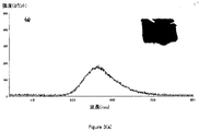
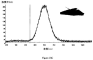
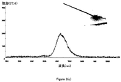
図3(a)〜図3(c)は、黄色、橙色及び赤色LEDのエレクトロルミネセンススペクトルをそれぞれ示す強度対波長グラフであり、これらの各々は上述の実施形態例を使用して得られる。114などのInリッチな量子ドット(図1)の成長中のTMInフロー及びInGaN量子井戸層116(図1)の成長温度が変化して、発光の色を変化させる。グラフは、約20mAの注入電流を使用して得た計測値に基づく。図3(a)〜図3(c)から、それぞれの黄色、橙色及び赤色LEDの強度は相対的に同じであることが観察される。それぞれの黄色、橙色及び赤色LEDの中心周波数が、互いに約20nmずつ偏位していることも観察される。 FIGS. 3 (a) -3 (c) are intensity vs. wavelength graphs showing the electroluminescence spectra of yellow, orange and red LEDs, respectively, each of which is obtained using the example embodiments described above. The TMIn flow during growth of In-rich quantum dots such as 114 (FIG. 1) and the growth temperature of the InGaN quantum well layer 116 (FIG. 1) change to change the color of light emission. The graph is based on measurements obtained using an injection current of about 20 mA. From FIG. 3 (a) to FIG. 3 (c), it is observed that the intensity of each yellow, orange and red LED is relatively the same. It is also observed that the center frequencies of the respective yellow, orange and red LEDs are offset from each other by approximately 20 nm.
図4は、別の実施形態例の調節可能な白色LED構造400を示す概略図である。処理チャンバ内にサファイア基板402が準備される。サファイア基板402上のGaNの核形成を促進するために、基板402上で低温バッファ層406を約520℃〜550℃の温度範囲で約25nmの厚みに成長させる。1018cm-3のドーピング濃度のGaNの層408を、層406上で約900℃〜1050℃の温度で成長させる。層408が成長した後、青色発光量子井戸構造410を形成させる。
FIG. 4 is a schematic diagram illustrating another example embodiment of an adjustable
青色発光量子井戸構造410を形成するために、GaNバリア層412を、約2×1017cm-3〜1×1018cm-3のSiドーピング濃度により約760℃〜850℃の温度で約5.0−15.0nmの厚みに成長させる。GaNバリア層412が成長した後、0.1<w<0.16のインジウム組成をもたらすために、バリア層412上で約2.0〜4.0nmの厚みを有するInWGa1-WN井戸層414を約760℃〜790℃の温度で成長させる。InGaN井戸層414が成長した後、InGaN井戸層414の上でGaNキャップ層416を成長させる。説明を明確にするために、図4には1つの量子井戸構造410のみを示している。当業者であれば、量子井戸構造410を成長させるためのステップを例えば3〜5回繰り返してMQW構造を形成できることを理解するであろう。
To form the blue light emitting
青色発光量子井戸構造410を形成した後、GaN層418を約740℃〜780℃の温度で約2×10¹⁷〜1×1018cm-3のSiドーピング濃度により約15〜30nmの厚みに成長させる。p−AlyGa1-yN(式中0.1<y<0.3)を含む電子ブロッキング層420を、約800℃〜1020℃で約20〜50nmの厚みに成長させる。p−AlyGa1-yNを成長させるためのTMAフローは、約750〜800℃の成長温度で約40〜100μモル/分に保持される。成長中、Cp2Mg源は約0.15〜0.5μモル/分に維持される。p−AlGaN層420が成長した後、p−GaN層422を、Mgをドーパントとして使用して約900℃〜1000℃で成長させる。この実施形態例では、層418、420及び422がp−GaNコンタクト構造424を形成する。p−GaNコンタクト構造424を形成した後、GaNキャップ層426を、p−GaNコンタクト構造424上で約800℃〜約1020℃の温度範囲で約10〜50nmの厚みに成長させる。GaNキャップ層426が成長して、p−GaN層422の表面を「平滑化」する。
After forming the blue light emitting
GaNキャップ層426が成長した後、赤色/黄色発光量子井戸構造428を成長させる。赤色/黄色発光量子井戸構造428を成長させるための処理ステップは、図1に関して赤色/黄色発光量子井戸構造122を成長させるために説明した処理ステップと実質的に同じである。この実施形態例では、InリッチなInGaN量子ドット成長中のTMInフロー及びInGaN井戸層の成長温度を約10℃〜30℃だけ変化させて、量子井戸構造428が黄色又は橙色光などの異なる波長の赤色ベースの色を発光できるようにすることができる。
After the
この実施形態例では、説明を明確にするために、図4には1つの量子井戸構造のみを示している。当業者であれば、量子井戸構造428を成長させるための処理ステップを例えば3〜5回繰り返してMQW構造を形成できることを理解するであろう(図1のMQW構造126と比較)。
In this example embodiment, only one quantum well structure is shown in FIG. 4 for clarity of explanation. One skilled in the art will appreciate that the processing steps for growing
量子井戸構造428が成長した後、p−InGaNコンタクト構造430を形成させる。p−InGaNコンタクト構造430を形成するための処理ステップは、図1に関してp−InGaNコンタクト層136を形成するために説明した処理ステップと実質的に同じである。
After the
図5は、上述の実施形態例の調節可能な白色LED構造400上の電気コンタクトの形成を示す概略図である。n−GaN層408の上部にある層が、誘導結合型プラズマエッチング(ICP)を使用してエッチングされる。次に、p−GaN層422の上部にある層がICPを使用してエッチングされる。n−GaN層408上にn−コンタクト502が形成され、p−GaN層422上にp−コンタクト504が形成され、p−InGaNコンタクト構造430のp−InGaN層上にp−コンタクト505が形成される。青色発光量子井戸構造410が、コンタクト502とコンタクト504との間のp−n接合を使用して活性化されるのに対し、黄色/赤色発光量子井戸構造428は、コンタクト502とコンタクト506との間のp−n接合を使用して活性化される。
FIG. 5 is a schematic diagram illustrating the formation of electrical contacts on the adjustable
上述の実施形態例では、青色発光量子井戸構造410から上層へと通過する青色光の一部を黄色/赤色発光量子井戸構造428が吸収し、黄色光として再発光することができる。すなわち、黄色/赤色発光量子井戸構造428からの黄色光成分は、(コンタクト502とコンタクト506との間のp−n接合に起因する)直接的なキャリアの再結合及び青色成分の一部の吸収の双方から生じる。さらに、黄色/赤色発光量子井戸構造428及び青色発光量子井戸構造410に様々な注入電流を別個に供給することができるので、LED構造400は調節可能な白色光を提供することができる。
In the above embodiment example, the yellow / red light emission quantum well structure 428 absorbs part of the blue light passing from the blue light emission quantum well structure 410 to the upper layer, and can re-emit light as yellow light. That is, the yellow light component from the yellow / red light emitting quantum well structure 428 causes direct carrier recombination (due to the pn junction between
別の実施形態例では、赤色/黄色発光量子井戸構造及び青色発光量子井戸構造の成長の順番を逆にすることができる。従って、この実施形態例では、最初にサファイア基板上で赤色/黄色発光量子井戸構造が成長し、これにp−InGaNコンタクト構造、青色発光量子井戸構造及びp−GaNコンタクト構造が続く。p−InGaNコンタクト構造を使用してp−n接合を形成して赤色/黄色発光量子井戸構造を活性化することができ、またp−GaNコンタクト構造を使用して別のp−n接合を形成して青色発光量子井戸構造を活性化することができる。 In another example embodiment, the order of growth of the red / yellow light emitting quantum well structure and the blue light emitting quantum well structure can be reversed. Thus, in this example embodiment, a red / yellow light emitting quantum well structure is first grown on a sapphire substrate, followed by a p-InGaN contact structure, a blue light emitting quantum well structure, and a p-GaN contact structure. A p-InGaN contact structure can be used to form a pn junction to activate a red / yellow light emitting quantum well structure, and a p-GaN contact structure can be used to form another pn junction. Thus, the blue light emitting quantum well structure can be activated.
上述の実施形態例では、青色発光量子井戸構造の前に黄色/赤色発光量子井戸構造が成長するので、黄色/赤色発光量子井戸構造から発光される黄色光は、p−InGaNコンタクト構造を使用して形成されたp−n接合にのみ基づく(すなわち、青色光の吸収を伴わない)。さらに、黄色/赤色発光量子井戸構造及び青色発光量子井戸構造に様々な注入電流を別個に供給することができるので、LED構造は調節可能な白色光を提供することができる。 In the above embodiment example, the yellow / red light emitting quantum well structure is grown before the blue light emitting quantum well structure. Therefore, the yellow light emitted from the yellow / red light emitting quantum well structure uses the p-InGaN contact structure. Only based on pn junctions formed (ie, without blue light absorption). In addition, the LED structure can provide tunable white light because different injection currents can be separately supplied to the yellow / red light emitting quantum well structure and the blue light emitting quantum well structure.
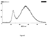
図6は、「冷度」調節可能な白色LEDのエレクトロルミネセンススペクトルを示す強度対波長のグラフである。この調節可能な白色LEDは、最初に黄色発光量子井戸構造が成長し、これに青色発光量子井戸構造が続くことを除き、調節可能な白色LED構造400(図4)と実質的に同じ処理条件を使用して形成される。 FIG. 6 is a graph of intensity versus wavelength showing the electroluminescence spectrum of a white LED with “coldness” tunable. This tunable white LED has substantially the same processing conditions as the tunable white LED structure 400 (FIG. 4), except that a yellow light emitting quantum well structure is first grown, followed by a blue light emitting quantum well structure. Formed using.
図7は、さらに別の実施形態例の調節可能な白色LED構造700を示す概略図である。LED構造700は、GaN層701と、GaN層701上で成長した青色/緑色発光量子井戸構造702と、量子井戸構造702上で成長したp−GaNコンタクト構造704と、p−GaNコンタクト構造704上で成長したGaNキャップ層706と、GaNキャップ層706上で成長した赤色/黄色発光量子井戸構造708とを含む。LED構造700を形成するための処理ステップは、赤色/黄色発光量子井戸構造708上にp−InGaNコンタクト構造が形成されないことを除き、図4に関するLED構造400を形成するための処理ステップと実質的に同じである。
FIG. 7 is a schematic diagram illustrating an adjustable
この実施形態例では、説明を明確にするために、図7には青色/緑色発光量子井戸構造702及び赤色/黄色発光量子井戸構造708ごとに1つの量子井戸構造を示している。当業者であれば、各々が青色/緑色光及び赤色/黄色光をそれぞれ発光するためのMQW構造を形成するためのそれぞれの量子井戸構造702及び708の形成中に、量子井戸構造702及び708を成長させるための処理ステップを、例えば3〜5回反復できることを理解するであろう(例えば、図1のMQW構造126と比較)。
In this example embodiment, for clarity of illustration, FIG. 7 shows one quantum well structure for each blue / green light emitting
この実施形態例では、GaN層701の上にある層が誘導結合型プラズマエッチング(ICP)を使用してエッチングされる。次いでp−GaNコンタクト構造704の上にある層がICPを使用してエッチングされる。GaN層701上にn−コンタクト710が形成され、p−GaNコンタクト構造704上にp−コンタクト712が形成される。青色/緑色発光量子井戸構造702が、コンタクト710とコンタクト712との間のp−n接合を使用して活性化されるのに対し、赤色/黄色発光量子井戸構造708は、青色/緑色発光量子井戸構造702から発光される青色光の吸収に基づいて活性化される。従って、この実施形態例では、赤色/黄色発光量子井戸構造708を活性化するための独立したp−n接合は存在しない。
In this example embodiment, the layer overlying
上述の実施形態例では、青色/緑色発光量子井戸構造702に様々な注入電流を供給することができるので、LED構造700は調節可能な白色光を提供することができる。当業者であれば、吸収可能な青色光の量に基づいて、赤色/黄色発光量子井戸構造708を間接的に「調節可能」にできることを理解するであろう。
In the example embodiment described above, various injection currents can be supplied to the blue / green light emitting quantum well structure 702 so that the
上述の実施形態例では、エレクトロルミネセンスの青色/緑色光をエレクトロルミネセンスの黄色/赤色光と混合することにより白色光が生成される。この実施形態例によりもたらされる1つの利点は、赤色/黄色発光量子井戸構造708が成長する前にp−GaNコンタクト構造704が成長するので、通常InN又はInリッチなナノ構造/量子ドットの外部拡散を生じるp−GaNコンタクト構造704の高温成長及びアニーリングがもはや懸案事項でなくなる点にある。この実施形態例は、GaN/InGaN結晶ベースの構造を提供することができ、現在の技術と比較してより良好な演色を実現することができる。この実施形態例では、GaNキャップ層706が、p−GaNコンタクト構造704からのMgの外部拡散を防ぐこともできる。
In the example embodiment described above, white light is produced by mixing electroluminescent blue / green light with electroluminescent yellow / red light. One advantage provided by this example embodiment is that the p-
図8は、さらに別の実施形態例における調節可能な白色LED構造800を示す概略図である。処理チャンバ内にサファイア基板802が準備される。サファイア基板402上のGaNの核形成を促進するために、基板802上で低温バッファ層806を約520℃〜550℃の温度範囲で約25nmの厚みに成長させる。1018cm-3のドーピング濃度を有するGaNの層808を、層806の上で約900℃〜1050℃の温度で成長させる。層808が成長した後、青色発光量子井戸構造810が形成される。
FIG. 8 is a schematic diagram illustrating a tunable
緑色発光量子井戸構造810を形成するために、GaNバリア層812を、約2×1017cm-3〜1×1018cm-3のSiドーピング濃度により約750℃〜850℃の温度で約5.0−15.0nmの厚みに成長させる。GaNバリア層812が成長した後、0.19<w<0.26のインジウム組成をもたらすために、約2.0〜4.0nmの厚みを有するInWGa1-WN井戸層814を、バリア層812上で約730℃〜770℃の温度で成長させる。InGaN井戸層814が成長した後、InGaN井戸層814上でGaNキャップ層816を成長させる。
To form the green light emitting
この実施形態例では、説明を明確にするために、図8には1つの緑色発光量子井戸構造のみを示している。当業者であれば、量子井戸構造810を成長させるための処理ステップを、例えば3〜5回繰り返してMQW構造を形成できることを理解するであろう。
In this embodiment, for the sake of clarity, only one green light emitting quantum well structure is shown in FIG. One skilled in the art will appreciate that the processing steps for growing
緑色発光量子井戸構造810を形成した後、緑色発光量子井戸構造810上でp−GaNコンタクト構造818を成長させる。p−GaNコンタクト構造818を成長させるための処理ステップは、図4に関するp−GaNコンタクト構造424を成長させるための処理ステップと実質的に同じである。p−GaNコンタクト構造818を形成した後、p−GaNコンタクト構造818上でGaNキャップ層820を成長させる。GaNキャップ層820が成長した後、GaNキャップ層820上に青色発光量子井戸構造822を形成させる。
After forming the green light emitting
青色発光量子井戸構造822を形成するための処理ステップは、図4に関する青色発光量子井戸構造410を形成するための処理ステップと実質的に同じである。この実施形態例では、説明を明確にするために、図8には1つの青色発光量子井戸構造のみを示している。当業者であれば、青色量子井戸構造822を成長させるための処理ステップを例えば3〜5回繰り返してMQW構造を形成できることを理解するであろう。
The processing steps for forming the blue light emitting
或いは、最初に青色発光量子井戸構造822を成長させ、これに緑色発光量子井戸構造810を続けることもできる。
Alternatively, the blue light emitting
この実施形態では、青色発光量子井戸構造822を形成した後、青色発光量子井戸構造822上で別のp−GaNコンタクト構造824を成長させる。p−GaNコンタクト構造824を成長させるための処理ステップは、図4に関するp−GaNコンタクト構造424を成長させるための処理ステップと実質的に同じである。p−GaNコンタクト構造824を形成した後、p−GaNコンタクト構造824上でGaNキャップ層826を成長させる。GaNキャップ層826が成長した後、GaNキャップ層826上に赤色発光量子井戸構造828が形成される。
In this embodiment, after forming the blue light emitting
赤色発光量子井戸構造828を形成するための処理ステップは、図1に関する赤色発光量子井戸構造122を形成するための処理ステップと実質的に同じである。この実施形態では、説明を明確にするために、図8には1つの赤色発光量子井戸構造のみを示している。当業者であれば、赤色量子井戸構造828を成長させるための処理ステップを例えば3〜5回反復してMQW構造を形成できることを理解するであろう(図1のMQW構造126を比較)。
The processing steps for forming the red light emitting
図9は、上述の実施形態例のLED構造800の電気コンタクトの形成を示す概略図である。GaN層808の上にある層が誘導結合型プラズマエッチング(ICP)を使用してエッチングされる。層808のエッチングに続き、p−GaNコンタクト構造818及びp−GaNコンタクト構造824の上にある層がICPを使用して順番にエッチングされる。GaN層808上にn−コンタクト902が形成され、p−GaNコンタクト構造818上にp−コンタクト904が形成され、p−GaNコンタクト構造824上にp−コンタクト906が形成される。緑色発光量子井戸構造810が、コンタクト902とコンタクト904との間のp−n接合を使用して活性化されるのに対し、青色発光量子井戸構造822は、コンタクト902とコンタクト906との間のp−n接合を使用して活性化される。赤色発光量子井戸構造828は、緑色及び青色発光量子井戸構造810、822からそれぞれ発光される青色/緑色光の吸収に基づいて活性化される。従って、この実施形態例では、赤色発光量子井戸構造828を活性化するための独立したp−n接合は存在しない。
FIG. 9 is a schematic diagram illustrating the formation of electrical contacts in the
上述の実施形態例では、緑色及び青色発光量子井戸構造810、822に様々な注入電流を供給することができるので、LED構造800は調節可能な白色光を提供することができる。当業者であれば、吸収可能な青色/緑色光の量に基づいて、赤色発光量子井戸構造828を間接的に「調節可能」にできることを理解するであろう。
In the example embodiments described above, the
上述の実施形態例は、より長い波長領域における発光を実現するためにインジウムリッチなInGaN量子ドットを利用してインジウムの取入れを促進する単色の黄色、橙色及び/又は赤色LEDを提供することができる。 The example embodiments described above can provide monochromatic yellow, orange and / or red LEDs that utilize indium-rich InGaN quantum dots to facilitate indium incorporation to achieve emission in longer wavelength regions. .
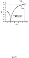
図10は、黄色LED構造(図3(a)を参照)及び白色LED構造(図4を参照)から得たI−V計測値を示す電流(I)対電圧(V)のグラフである。プロット1002は黄色LED構造から得た計測値に基づき、プロット1004は白色LED構造から得た計測値に基づく。それぞれのLED構造が安定した従来のダイオード特性を示すことがプロット1002、1004から観察できる。
FIG. 10 is a graph of current (I) versus voltage (V) showing IV measurements obtained from a yellow LED structure (see FIG. 3A) and a white LED structure (see FIG. 4). The
図11は、図4に関する白色LED構造400の表面モルフォロジーを示す走査電子顕微鏡(SEM)画像1102である。画像1102に示すように、p−InGaNコンタクト構造430(図4)のp−InGaN層は多孔質様の表面を有し、これが散乱効果を与えることにより、410、428などの量子井戸構造(図4)からの光抽出を促進する。
FIG. 11 is a scanning electron microscope (SEM)
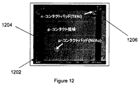
図12は、図7に関する白色LED構造700の表面モルフォロジーを示す走査電子顕微鏡(SEM)画像1202である。画像1202は、Ni/Auコンタクトパッド1204としてp−コンタクトを、Ti/Alコンタクトパッド1208としてn−コンタクトを示している。
FIG. 12 is a scanning electron microscope (SEM)
図13は、図12の画像1202を拡大した走査電子顕微鏡(SEM)画像1302である。画像1302に示すように、p−コンタクトは1304のようなNi/Au金属ストライプの形であり、1304のようなストライプの間に赤色/黄色発光量子井戸構造の表面1306が見える。
FIG. 13 is a scanning electron microscope (SEM)
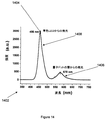
図14は、図12及び図13のサンプル白色LED構造のエレクトロルミネセンススペクトルを示す強度対波長のグラフ1402である。グラフ1402は、約456nmで発光ピーク1404を示す。発光1408の発光ピーク1404は、青色/緑色発光量子井戸構造により生み出される。グラフ1402はまた、幅広かつ低強度の発光1406も示す。発光1406は、赤色/黄色発光量子井戸構造により生み出される。当業者であれば、赤色/黄色発光量子井戸構造は、青色/緑色発光量子井戸構造から発光される青色光の吸収に基づいて活性化されるので、青色発光1408よりも赤色/黄色発光1406の方が強度が低いことを理解するであろう。
FIG. 14 is an intensity vs.
図15は、図12及び図13のサンプル白色LED構造から得たI−V計測値を示す電流(I)対電圧(V)のグラフ1502である。白色LED構造が、約3Vのターンオン電圧と約5Vで約60mAの電流とを有する良好なI−V特性を示すことがグラフ1502から観察できる。
FIG. 15 is a
図16は、発光ダイオードのためのMQW構造を作製する方法を示すフロー図である。ステップ1602において、複数の量子井戸構造が形成される。個々の量子井戸構造は、バリア層と、バリア層上に形成され量子ドットナノ構造を組み込んだ井戸層とを含み、バリア層及び井戸層は第1の金属窒化物ベースの材料を含む。ステップ1604において、量子井戸構造の少なくとも1つが井戸層上にキャッピング層をさらに含むように形成され、キャッピング層は第1の金属窒化物ベースの材料と比較して異なる金属成分を有する第2の金属窒化物ベースの材料を含む。
FIG. 16 is a flow diagram illustrating a method of fabricating an MQW structure for a light emitting diode. In
図17は、発光ダイオード構造を作製する方法を示すフロー図である。ステップ1702において、赤色/黄色発光多重量子井戸(MQW)構造が形成される。赤色/黄色発光MQWの個々の量子井戸構造は、バリア層と、バリア層上に形成され量子ドットナノ構造を組み込んだ井戸層とを含み、バリア層及び井戸層は第1の金属窒化物ベースの材料を含む。ステップ1704において、赤色/黄色発光MQWの量子井戸構造の少なくとも1つが井戸層上にキャッピング層をさらに含むように形成され、キャッピング層は第1の金属窒化物ベースの材料と比較して異なる金属成分を有する第2の金属窒化物ベースの材料を含む。ステップ1706において、発光ダイオード構造から白色光を発光するために赤色/黄色発光MQWと一体に青色発光MQW構造が形成される。
FIG. 17 is a flow diagram illustrating a method for fabricating a light emitting diode structure. In
図18は、発光ダイオードを作製する別の方法を示すフロー図である。ステップ1802において、赤色/黄色発光多重量子井戸(MQW)構造が形成される。赤色/黄色発光MQWの個々の量子井戸構造は、バリア層と、バリア層上に形成され量子ドットナノ構造を組み込んだ井戸層とを含み、バリア層及び井戸層は第1の金属窒化物ベースの材料を含む。ステップ1804において、赤色/黄色発光MQWの量子井戸構造の少なくとも1つが井戸層上にキャッピング層をさらに含むように形成され、キャッピング層は第1の金属窒化物ベースの材料と比較して異なる金属成分を有する第2の金属窒化物ベースの材料を含む。ステップ1806において、青色発光MQW構造が赤色/黄色発光MQWと一体に形成される。ステップ1808において、発光ダイオード構造から白色光を発光するために赤色/黄色発光MQW及び青色発光MQW構造と一体に緑色発光MQW構造が形成される。
FIG. 18 is a flow diagram illustrating another method for fabricating a light emitting diode. In
上述の実施形態では、井戸層に組み込まれたInリッチなInGaN量子ドット又はナノ構造を使用して、赤色、琥珀色及び/又は黄色光を生成する。高温の原位置アニーリング中などにおけるGaNバリアへの外部拡散を防止するために、個々の活性量子井戸層は薄いAlN層により封入される。白色光を生成するために、異なる色のMQWの組み合わせを単一のLED構造内に組み入れることができる。従って、説明した実施形態例のデバイスを作動させるために複雑な回路を使用する必要性をなくすことができる。さらに、蛍光体を使用しないので作製技術を単純化することができ、この実施形態例により、通常のRGB LEDの場合のような蛍光体の劣化、及び異なる材料ベースのLEDの異なる劣化作用の問題を解決することができる。説明した実施形態例はまた、LEDチップ上の蛍光体の外部コーティングの使用を排除することもできる。また、説明した実施形態例におけるInリッチなInGaN量子ドットの取入れが、再結合効率をさらに高めるとともに、高温作動時などにおけるより良好な安定性を提供することができる。 In the embodiments described above, In-rich InGaN quantum dots or nanostructures incorporated in the well layer are used to generate red, amber and / or yellow light. In order to prevent external diffusion into the GaN barrier, such as during high temperature in-situ annealing, the individual active quantum well layers are encapsulated by a thin AlN layer. To produce white light, a combination of different color MQWs can be incorporated into a single LED structure. Thus, the need to use complex circuitry to operate the devices of the described example embodiments can be eliminated. Furthermore, since no phosphor is used, the fabrication technique can be simplified, and this example embodiment presents the problem of phosphor degradation as in the case of normal RGB LEDs, and different degradation effects of different material based LEDs. Can be solved. The described example embodiments can also eliminate the use of a phosphor outer coating on the LED chip. Also, the incorporation of In-rich InGaN quantum dots in the described example embodiments can further increase recombination efficiency and provide better stability during high temperature operation and the like.
さらに、個々の量子井戸構造から青色、緑色及び赤色という個々の原色の発光を行うことができる説明した実施形態例では、ドットサイズ及びIn組成を制御することにより、例えば「冷」白色、「リンゴ」白色又は「暖」白色などの異なる品質の白色を得ることができる。 Furthermore, in the described exemplary embodiment that can emit individual primary colors of blue, green and red from individual quantum well structures, for example, by controlling dot size and In composition, for example “cold” white, “apple” Different quality whites can be obtained, such as “white” or “warm” white.
背景技術の項で説明したように、GaN LEDの生産は、主にInGaN層内の高インジウム取り入れを得ることが困難であることに起因して実際的に困難である。通常これは、インジウムの固体非混和性及び高温での分解に起因して生じる。上述の実施形態例では、TMIバーストステップ中のインジウムの取入れを促進するために薄いInGaN湿潤層を使用する。これにより、発光波長を赤色波長領域内に押しこむことが判明しているインジウムリッチなInGaN量子ドットの形成を促進することができる。例えば、より長い波長領域などにおいて単色の発光色を得るために、Inリッチな量子ドット及びInGaN井戸の成長中の温度は安定した状態に保たれる。この温度の変動は、電圧バイアスが印加された際に波長のわずかな変化につながる可能性がある。さらに、温度に関しては、p−GaN層を約900℃の温度で成長させた場合、形成されたインジウムリッチなInGaN量子ドットが、通常、井戸層内などに拡散するとともにバリア層内にも拡散する。説明した実施形態例では、p−InGaN層の成長中、温度が約750℃〜約800℃に下げられる。約800℃〜850℃での原位置アニーリングが、量子ドット内のインジウムの拡散により発光波長をシフトさせる可能性があることを理解できよう。従って、説明した実施形態例では、AlN層を使用することにより、p−InGaN層の成長中、高温におけるその他の層の成長中、及び/又は約800℃〜850℃での原位置アニーリング中におけるインジウムの量子ドットからの外部拡散を防ぐことができる。また、説明した実施形態例は、GaN LEDから原色の発光を得ることができ、これが固体照明のためのより良好な白色光の演色を可能にすることができる。 As explained in the background section, the production of GaN LEDs is practically difficult mainly due to the difficulty in obtaining high indium incorporation in the InGaN layer. This usually occurs due to the solid immiscibility of indium and the decomposition at high temperatures. In the example embodiment described above, a thin InGaN wetting layer is used to facilitate indium uptake during the TMI burst step. This can facilitate the formation of indium-rich InGaN quantum dots that have been found to push the emission wavelength into the red wavelength region. For example, the temperature during growth of In-rich quantum dots and InGaN wells is kept stable in order to obtain a monochromatic emission color in a longer wavelength region or the like. This temperature variation can lead to a slight change in wavelength when a voltage bias is applied. Further, regarding the temperature, when the p-GaN layer is grown at a temperature of about 900 ° C., the formed indium-rich InGaN quantum dots usually diffuse into the well layer and the like as well as into the barrier layer. . In the example embodiment described, the temperature is lowered to about 750 ° C. to about 800 ° C. during the growth of the p-InGaN layer. It will be appreciated that in situ annealing at about 800 ° C. to 850 ° C. may shift the emission wavelength due to indium diffusion within the quantum dots. Thus, in the described example embodiment, an AlN layer is used to grow a p-InGaN layer, during growth of other layers at high temperatures, and / or during in situ annealing at about 800 ° C. to 850 ° C. External diffusion from indium quantum dots can be prevented. The described example embodiments can also obtain primary color emission from GaN LEDs, which can allow better white light color rendering for solid state lighting.
上述した実施形態例を使用して、看板及びディスプレイの照明、キーパッド導光、デジタルカメラのフラッシュ光、PCモニタのバックライト、演色、固体照明を含む照明及び表示目的、及び自動車のテールライト及び交通信号灯などの数多くの用途にInGaN量子ドットLEDを使用することができる。 Using the example embodiments described above, signage and display lighting, keypad light guiding, digital camera flash light, PC monitor backlighting, color rendering, lighting and display purposes including solid state lighting, and automotive taillights and InGaN quantum dot LEDs can be used for many applications such as traffic lights.
当業者であれば、従来の有機LED(OLED)は、黄色、橙色及び赤色によるフレキシブルディスプレイを提供することができるが、通常OLEDは、光束及びルミネセンス効率に関してはこの実施形態例のような無機LEDに劣ることを理解するであろう。 One skilled in the art can provide conventional organic LEDs (OLEDs) to provide flexible displays in yellow, orange and red, but typically OLEDs are inorganic as in this embodiment with respect to luminous flux and luminescence efficiency. You will understand that it is inferior to LED.
当業者であれば、広範にわたって説明した本発明の思想及び範囲から逸脱することなく、特定の実施形態の形で示した本発明に対して数多くの変更及び/又は修正を行うことができることを理解するであろう。従ってあらゆる点において、本実施形態は限定的なものではなく例示的なものであると見なすべきである。 Those skilled in the art will appreciate that numerous changes and / or modifications can be made to the invention shown in the form of specific embodiments without departing from the spirit and scope of the invention as broadly described. Will do. Accordingly, in all respects, this embodiment should be considered exemplary rather than limiting.
Claims (28)
前記MQW構造が複数の量子井戸構造を含み、個々の量子井戸構造が、
バリア層と、
前記バリア層上に形成され量子ドットナノ構造を組み込んだ井戸層と、
を含み、前記バリア層及び前記井戸層が第1の金属窒化物ベースの材料を含み、
前記量子井戸構造の少なくとも1つが、前記第1の金属窒化物ベースの材料と比較して異なる金属元素を有する第2の金属窒化物ベースの材料を含む、前記井戸層上に形成されたキャッピング層と、
前記第2の金属窒化物ベースの材料と比較して異なる金属元素を有する第3の金属窒化物ベースの材料を含む、前記キャッピング層上に形成された第2のキャッピング層とを、 さらに含むことを特徴とするMQW構造。 A multiple quantum well (MQW) structure for a light emitting diode,
The MQW structure includes a plurality of quantum well structures, and each quantum well structure includes:
A barrier layer;
A well layer formed on the barrier layer and incorporating quantum dot nanostructures;
The barrier layer and the well layer comprise a first metal nitride based material;
A capping layer formed on the well layer, wherein at least one of the quantum well structures includes a second metal nitride-based material having a different metal element compared to the first metal nitride-based material When,
A second capping layer formed on the capping layer, wherein the second capping layer includes a third metal nitride-based material having a different metal element compared to the second metal nitride-based material. MQW structure characterized by
ことを特徴とする請求項1に記載のMQW構造。 Each quantum well structure further includes a wetting layer formed between the barrier layer and the well layer to facilitate the formation of the quantum dot nanostructure.
The MQW structure according to claim 1, wherein:
ことを特徴とする請求項1から請求項2のいずれか1項に記載のMQW構造。 The MQW structure further includes a p-type contact structure formed on the outermost structure of the plurality of quantum well structures, and the p-type contact structure is formed on the electron blocking layer and the electron blocking layer. a p-type metal nitride layer,
The MQW structure according to any one of claims 1 to 2, wherein the MQW structure is provided.
ことを特徴とする請求項3に記載のMQW構造。 The p-type metal nitride layer includes an indium (In) material;
The MQW structure according to claim 3.
ことを特徴とする請求項4に記載のMQW構造。 The p-type metal nitride layer is formed using a temperature between about 750 ° C. and 800 ° C .;
The MQW structure according to claim 4.
ことを特徴とする請求項1から請求項5のいずれか1項に記載のMQW構造。 The MQW structure further includes an n-type contact layer for making electrical contact with an n + layer underlying the plurality of quantum well structures;
The MQW structure according to any one of claims 1 to 5, wherein the MQW structure is provided.
ことを特徴とする請求項1から請求項6のいずれか1項に記載のMQW構造。 The MQW structure can emit light in a wavelength range from red to yellow;
The MQW structure according to any one of claims 1 to 6, wherein the MQW structure is provided.
ことを特徴とする請求項1から請求項7のいずれか1項に記載のMQW構造。 The MQW structure can emit red light;
The MQW structure according to any one of claims 1 to 7, wherein the MQW structure is provided.
ことを特徴とする請求項1から請求項8のいずれか1項に記載のMQW構造。 The capping layer comprises an aluminum nitride (AlN) material;
The MQW structure according to any one of claims 1 to 8, wherein the MQW structure is provided.
ことを特徴とする請求項1から請求項9のいずれか1項に記載のMQW構造。 The thickness of the capping layer is maintained at about 3 nm or less,
The MQW structure according to any one of claims 1 to 9, wherein the MQW structure is provided.
赤色から黄色までの波長範囲の光を発光する赤色/黄色発光の多重量子井戸(MQW)構造を含み、該赤色/黄色発光のMQWの個々の量子井戸構造が、
バリア層と、
前記バリア層上に形成され量子ドットナノ構造を組み込んだ井戸層と、
を含み、前記バリア層及び前記井戸層が第1の金属窒化物ベースの材料を含み、
前記赤色/黄色発光のMQWの前記量子井戸構造の少なくとも1つが、前記井戸層上に形成されたキャッピング層をさらに含み、該キャッピング層が、前記第1の金属窒化物ベースの材料と比較して異なる金属元素を有する第2の金属窒化物ベースの材料を含み、そして、前記キャッピング層上に形成された第2のキャッピング層をさらに含み、該第2のキャッピング層が、前記第2の金属窒化物ベースの材料と比較して異なる金属成分を有する第3の金属窒化物ベースの材料を含み、
前記発光ダイオード構造がさらに、
前記発光ダイオード構造から白色光を発光するために前記赤色/黄色発光のMQWと一体に形成された青色発光のMQW構造を含む、
ことを特徴とする発光ダイオード構造。 A light emitting diode structure,
A red / yellow emitting multiple quantum well (MQW) structure that emits light in the wavelength range from red to yellow, wherein the individual quantum well structures of the red / yellow emitting MQW include:
A barrier layer;
A well layer formed on the barrier layer and incorporating quantum dot nanostructures;
The barrier layer and the well layer comprise a first metal nitride based material;
At least one of the quantum well structures of the red / yellow emitting MQW further comprises a capping layer formed on the well layer, the capping layer being compared to the first metal nitride based material. A second metal nitride-based material having a different metal element, and further comprising a second capping layer formed on the capping layer, wherein the second capping layer comprises the second metal nitride. A third metal nitride based material having a different metal component compared to the material based material;
The light emitting diode structure further includes:
A blue light emitting MQW structure formed integrally with the red / yellow light emitting MQW to emit white light from the light emitting diode structure;
A light emitting diode structure characterized by that.
ことを特徴とする請求項12に記載の発光ダイオード構造。 The blue light emitting MQW is formed on the outermost structure of the plurality of quantum well structures of the red / yellow light emitting MQW structure.
The light emitting diode structure according to claim 12.
ことを特徴とする請求項12に記載の発光ダイオード構造。 The red / the plurality of quantum well structure of the yellow emission of MQW structure is formed on the MQW structure of the blue-emitting,
The light emitting diode structure according to claim 12.
ことを特徴とする請求項12から請求項14のいずれか1項に記載の発光ダイオード構造。 An n-type contact layer for making electrical contact with the n + layer under the red / yellow light emission and blue light emission MQW structures, and each p formed on the red / yellow light emission and blue light emission MQW structures. A p-type contact structure, each of the p-type contact structures including an electron blocking layer and a p-type metal nitride layer formed on the electron blocking layer.
The light emitting diode structure according to claim 12, wherein the light emitting diode structure is a light emitting diode structure.
ことを特徴とする請求項14に記載の発光ダイオード構造。 An n-type contact layer for making electrical contact with the n + layer under the blue light emitting MQW structure, and a p formed on the blue light emitting MQW structure for activating the blue light emitting MQW structure. A red / yellow light emitting MQW structure, which can emit light in a wavelength range from red to yellow based on absorption of blue light emission from the blue light emitting MQW structure.
The light emitting diode structure according to claim 14.
請求項12から請求項16のいずれか1項に記載の発光ダイオード構造。 The capping layer comprises an aluminum nitride (AlN) material;
The light emitting diode structure according to any one of claims 12 to 16.
ことを特徴とする請求項12から請求項17のいずれか1項に記載のMQW構造。 The thickness of the capping layer is maintained at about 3 nm or less,
The MQW structure according to any one of claims 12 to 17, wherein the MQW structure is provided.
赤色から黄色までの波長範囲の光を発光する赤色/黄色発光の多重量子井戸(MQW)構造を含み、該赤色/黄色発光のMQWの個々の量子井戸構造が、
バリア層と、
前記バリア層上に形成され量子ドットナノ構造を組み込んだ井戸層と、
を含み、前記バリア層及び前記井戸層が第1の金属窒化物ベースの材料を含み、
前記赤色/黄色発光のMQWの前記量子井戸構造の少なくとも1つが、前記井戸層上に形成されたキャッピング層をさらに含み、該キャッピング層が、前記第1の金属窒化物ベースの材料と比較して異なる金属元素を有する第2の金属窒化物ベースの材料を含み、そして、前記キャッピング層上に形成された第2のキャッピング層をさらに含み、該第2のキャッピング層が、前記第2の金属窒化物ベースの材料と比較して異なる金属成分を有する第3の金属窒化物ベースの材料を含み、
前記発光ダイオード構造がさらに、
青色発光のMQW構造と、
緑色発光のMQW構造と、
を含み、前記発光ダイオード構造から白色光を発光するために前記青色発光のMQW構造及び前記緑色発光のMQW構造が前記赤色/黄色発光のMQWと一体に形成される、
ことを特徴とする発光ダイオード構造。 A light emitting diode structure,
A red / yellow emitting multiple quantum well (MQW) structure that emits light in the wavelength range from red to yellow, wherein the individual quantum well structures of the red / yellow emitting MQW include:
A barrier layer;
A well layer formed on the barrier layer and incorporating quantum dot nanostructures;
The barrier layer and the well layer comprise a first metal nitride based material;
At least one of the quantum well structures of the red / yellow emitting MQW further comprises a capping layer formed on the well layer, the capping layer being compared to the first metal nitride based material. A second metal nitride-based material having a different metal element, and further comprising a second capping layer formed on the capping layer, wherein the second capping layer comprises the second metal nitride. A third metal nitride based material having a different metal component compared to the material based material;
The light emitting diode structure further includes:
A blue-emitting MQW structure;
MQW structure with green emission,
The blue light emitting MQW structure and the green light emitting MQW structure are formed integrally with the red / yellow light emitting MQW to emit white light from the light emitting diode structure.
A light emitting diode structure characterized by that.
ことを特徴とする請求項20に記載の発光ダイオード構造。 The red / yellow light emitting MQW structure is formed on the blue light emitting MQW structure and the green light emitting MQW structure.
The light-emitting diode structure according to claim 20.
前記青色発光のMQW構造及び前記緑色発光のMQW構造をそれぞれ活性化するための、前記青色発光のMQW構造及び前記緑色発光のMQW構造上に形成されたそれぞれのp型コンタクト構造と、
をさらに含み、
前記p型コンタクト構造が各々、電子ブロッキング層と、前記電子ブロッキング層上に形成されたp型金属窒化物層とを含み、さらに前記赤色/黄色発光のMQW構造が、前記青色発光のMQW構造からの青色発光、前記緑色発光のMQW構造からの緑色発光、又はこれらの両方の吸収に基づいて赤色から黄色までの波長範囲の光を発光することができる、
ことを特徴とする請求項20又は請求項21に記載の発光ダイオード構造。 An n-type contact layer for making electrical contact with the n + layer under the red / yellow emission, blue emission and green emission MQW structures;
P-type contact structures formed on the blue light-emitting MQW structure and the green light-emitting MQW structure, respectively, for activating the blue light-emitting MQW structure and the green light-emitting MQW structure;
Further including
Each of the p-type contact structures includes an electron blocking layer and a p-type metal nitride layer formed on the electron blocking layer, and the red / yellow light emitting MQW structure is different from the blue light emitting MQW structure. Can emit light in the wavelength range from red to yellow based on absorption of both blue emission, green emission from the green emission MQW structure, or both of these,
The light-emitting diode structure according to claim 20 or claim 21, wherein
ことを特徴とする請求項20から請求項22のいずれか1項に記載の発光ダイオード構造。 The capping layer comprises an aluminum nitride (AlN) material;
The light-emitting diode structure according to any one of claims 20 to 22, wherein the light-emitting diode structure is provided.
ことを特徴とする請求項20から請求項23のいずれか1項に記載の発光ダイオード構造。 The thickness of the capping layer is maintained at about 3 nm or less,
24. The light-emitting diode structure according to claim 20, wherein the light-emitting diode structure is a light-emitting diode structure.
複数の量子井戸構造であって、各々がバリア層と、前記バリア層上に形成され量子ドットナノ構造を組み込んだ井戸層とを含み、前記バリア層及び前記井戸層が第1の金属窒化物ベースの材料を含む複数の量子井戸構造を形成するステップと、
前記第1の金属窒化物ベースの材料と比較して異なる金属元素を有する第2の金属窒化物ベースの材料を含む、前記井戸層上のキャッピング層と、前記第2の金属窒化物ベースの材料と比較して異なる金属元素を有する第3の金属窒化物ベースの材料を含む、前記キャッピング層上に形成された第2のキャッピング層とを、含むように前記量子井戸構造の少なくとも1つを形成するステップと、
を含むことを特徴とする方法。 A method of fabricating a multiple quantum well (MQW) structure for a light emitting diode, comprising:
A plurality of quantum well structures, each comprising a barrier layer and a well layer formed on the barrier layer and incorporating a quantum dot nanostructure, wherein the barrier layer and the well layer are based on a first metal nitride base Forming a plurality of quantum well structures comprising materials;
A capping layer on the well layer, the second metal nitride based material comprising a second metal nitride based material having a different metal element compared to the first metal nitride based material; Forming at least one of said quantum well structures to include a second capping layer formed on said capping layer comprising a third metal nitride based material having a different metal element compared to And steps to
A method comprising the steps of:
多重量子井戸構造であって(MQW)、各々の量子井戸構造がバリア層と、前記バリア層上に形成され量子ドットナノ構造を組み込んだ井戸層とを含み、前記バリア層及び前記井戸層が第1の金属窒化物ベースの材料を含む、赤色から黄色までの波長範囲の光を発光する赤色/黄色発光の多重量子井戸構造を形成するステップと、
前記第1の金属窒化物ベースの材料と比較して異なる金属元素を有する第2の金属窒化物ベースの材料を含むキャッピング層を前記井戸層上にさらに含み、そして、前記第2の金属窒化物ベースの材料と比較して異なる金属成分を有する第3の金属窒化物ベースの材料を含む、前記キャッピング層上に形成された第2のキャッピング層をさらに含むように、前記赤色/黄色発光のMQWの前記量子井戸構造の少なくとも1つを形成するステップと、
前記発光ダイオード構造から白色光を発光するために前記赤色/黄色発光のMQWと一体に青色発光のMQW構造を形成するステップと、
を含むことを特徴とする方法。 A method for fabricating a light emitting diode structure comprising:
A multiple quantum well structure (MQW), each quantum well structure including a barrier layer and a well layer formed on the barrier layer and incorporating a quantum dot nanostructure, wherein the barrier layer and the well layer are first Forming a red / yellow emitting multiple quantum well structure that emits light in the wavelength range from red to yellow, comprising a metal nitride based material of:
Further seen including a capping layer on the well layer comprising a second metal-nitride based material having a metal element different compared to the first metal-nitride based material, and the second metal nitride The red / yellow light emitting material further includes a second capping layer formed on the capping layer, the third capping layer comprising a third metal nitride based material having a different metal component compared to the material based material . Forming at least one of said quantum well structures of MQW;
Forming a blue emitting MQW structure integrally with the red / yellow emitting MQW to emit white light from the light emitting diode structure;
A method comprising the steps of:
多重量子井戸構造であって(MQW)、各々の量子井戸構造がバリア層と、前記バリア層上に形成され量子ドットナノ構造を組み込んだ井戸層とを含み、前記バリア層及び前記井戸層が第1の金属窒化物ベースの材料を含む、赤色から黄色までの波長範囲の光を発光する赤色/黄色発光の多重量子井戸構造を形成するステップと、
前記第1の金属窒化物ベースの材料と比較して異なる金属元素を有する第2の金属窒化物ベースの材料を含むキャッピング層を前記井戸層上にさらに含み、そして、前記第2の金属窒化物ベースの材料と比較して異なる金属成分を有する第3の金属窒化物ベースの材料を含む、前記キャッピング層上に形成された第2のキャッピング層をさらに含むように、前記赤色/黄色発光のMQWの前記量子井戸構造の少なくとも1つを形成するステップと、
前記赤色/黄色発光のMQWと一体に青色発光のMQW構造を形成するステップと、
前記発光ダイオード構造から白色光を発光するために前記赤色/黄色発光のMQW及び前記青色発光のMQW構造と一体に緑色発光のMQW構造を形成するステップと、
を含むことを特徴とする方法。 A method for fabricating a light emitting diode structure comprising:
A multiple quantum well structure (MQW), each quantum well structure including a barrier layer and a well layer formed on the barrier layer and incorporating a quantum dot nanostructure, wherein the barrier layer and the well layer are first Forming a red / yellow emitting multiple quantum well structure that emits light in the wavelength range from red to yellow, comprising a metal nitride based material of:
Further seen including a capping layer on the well layer comprising a second metal-nitride based material having a metal element different compared to the first metal-nitride based material, and the second metal nitride a third metal nitride based material having a different metal components as compared to the object-based material, the second capping layer further contains useless formed capping layer, the red / yellow light emitting MQW Forming at least one of said quantum well structures of:
Forming a blue light emitting MQW structure integrally with the red / yellow light emitting MQW;
Forming a green light emitting MQW structure integrally with the red / yellow light emitting MQW structure and the blue light emitting MQW structure to emit white light from the light emitting diode structure;
A method comprising the steps of:
Applications Claiming Priority (1)
| Application Number | Priority Date | Filing Date | Title |
|---|---|---|---|
| PCT/SG2007/000350 WO2009048425A1 (en) | 2007-10-12 | 2007-10-12 | Fabrication of phosphor free red and white nitride-based leds |
Publications (2)
| Publication Number | Publication Date |
|---|---|
| JP2011501408A JP2011501408A (en) | 2011-01-06 |
| JP5437253B2 true JP5437253B2 (en) | 2014-03-12 |
Family
ID=40549418
Family Applications (1)
| Application Number | Title | Priority Date | Filing Date |
|---|---|---|---|
| JP2010528843A Expired - Fee Related JP5437253B2 (en) | 2007-10-12 | 2007-10-12 | Fabrication of red and white nitride based LEDs without phosphors |
Country Status (6)
| Country | Link |
|---|---|
| US (1) | US8436334B2 (en) |
| JP (1) | JP5437253B2 (en) |
| KR (1) | KR101404143B1 (en) |
| CN (1) | CN101821861B (en) |
| TW (1) | TWI381554B (en) |
| WO (1) | WO2009048425A1 (en) |
Families Citing this family (40)
| Publication number | Priority date | Publication date | Assignee | Title |
|---|---|---|---|---|
| US6958497B2 (en) * | 2001-05-30 | 2005-10-25 | Cree, Inc. | Group III nitride based light emitting diode structures with a quantum well and superlattice, group III nitride based quantum well structures and group III nitride based superlattice structures |
| TWI396294B (en) * | 2008-11-12 | 2013-05-11 | Academia Sinica | Quantum dot infrared photodetector apparatus |
| WO2010123809A2 (en) | 2009-04-20 | 2010-10-28 | 3M Innovative Properties Company | Non-radiatively pumped wavelength converter |
| US8455903B2 (en) * | 2009-04-20 | 2013-06-04 | 3M Innovative Properties Company | Non-radiatively pumped wavelength converter |
| KR100993074B1 (en) * | 2009-12-29 | 2010-11-08 | 엘지이노텍 주식회사 | Light emitting device, method for fabricating the same and light emitting device package |
| US20110237011A1 (en) * | 2010-03-29 | 2011-09-29 | Nanjing University | Method for Forming a GaN-Based Quantum-Well LED with Red Light |
| JP5197686B2 (en) | 2010-07-16 | 2013-05-15 | 株式会社東芝 | Manufacturing method of semiconductor light emitting device |
| JP2012129340A (en) * | 2010-12-15 | 2012-07-05 | Toshiba Corp | Semiconductor light-emitting element |
| CN102208503A (en) * | 2011-01-25 | 2011-10-05 | 中山大学佛山研究院 | Light-emitting diode (LED) epitaxial structure and manufacturing method thereof |
| ES2616308T3 (en) | 2011-03-17 | 2017-06-12 | Valoya Oy | Method for dark growth chambers |
| DE11158693T8 (en) | 2011-03-17 | 2013-04-25 | Valoya Oy | Plant lighting device and method |
| EP2499900A1 (en) | 2011-03-17 | 2012-09-19 | Valoya Oy | Method and means for enhancing greenhouse lights |
| JP5060637B1 (en) * | 2011-05-13 | 2012-10-31 | 株式会社東芝 | Semiconductor light emitting device and wafer |
| CN102231422A (en) * | 2011-06-16 | 2011-11-02 | 清华大学 | Fluorescent-powder-free single-chip GaN (gallium nitride)-based LED (light-emitting diode) and manufacturing method thereof |
| CN102339919A (en) * | 2011-10-21 | 2012-02-01 | 西安重装渭南光电科技有限公司 | Epitaxial structure and process for LEDs (light-emitting diodes) |
| KR101903361B1 (en) | 2012-03-07 | 2018-10-04 | 삼성전자주식회사 | Nitride semiconductor light emitting device and manufacturing method thereof |
| CN104205369A (en) * | 2012-03-19 | 2014-12-10 | 皇家飞利浦有限公司 | Light emitting device grown on a silicon substrate |
| CN103367342B (en) * | 2012-03-30 | 2016-07-06 | 华夏光股份有限公司 | Stacking in conjunction with light emitting diode |
| KR101373804B1 (en) * | 2012-06-19 | 2014-03-14 | 광주과학기술원 | White light emitting diode and fabrication method thereof |
| CN103545170A (en) * | 2012-07-13 | 2014-01-29 | 华夏光股份有限公司 | Semiconductor device and production method thereof |
| US9082637B2 (en) * | 2012-08-17 | 2015-07-14 | The University Of Connecticut | Optoelectronic integrated circuit |
| JP6001446B2 (en) * | 2012-12-28 | 2016-10-05 | 株式会社東芝 | Semiconductor light emitting device and manufacturing method thereof |
| CN103165774B (en) * | 2013-02-28 | 2015-09-23 | 溧阳市宏达电机有限公司 | A kind of silicon carbide epitaxy light-emitting diode of ledge structure |
| JP6174499B2 (en) * | 2014-01-27 | 2017-08-02 | 株式会社Qdレーザ | Semiconductor light emitting device |
| JP6367590B2 (en) * | 2014-03-31 | 2018-08-01 | 日本碍子株式会社 | LIGHT EMITTING ELEMENT AND METHOD FOR MANUFACTURING LIGHT EMITTING ELEMENT STRUCTURE |
| FR3019380B1 (en) * | 2014-04-01 | 2017-09-01 | Centre Nat Rech Scient | PIXEL SEMICONDUCTOR, MATRIX OF SUCH PIXELS, SEMICONDUCTOR STRUCTURE FOR CARRYING OUT SUCH PIXELS AND METHODS OF MAKING SAME |
| TWI533467B (en) * | 2014-05-13 | 2016-05-11 | 國立中山大學 | An epitaxy structure of light emitting elements |
| US9590140B2 (en) * | 2014-07-03 | 2017-03-07 | Sergey Suchalkin | Bi-directional dual-color light emitting device and systems for use thereof |
| US9865772B2 (en) * | 2015-01-06 | 2018-01-09 | Apple Inc. | LED structures for reduced non-radiative sidewall recombination |
| US11552057B2 (en) * | 2017-12-20 | 2023-01-10 | Seoul Viosys Co., Ltd. | LED unit for display and display apparatus having the same |
| CN108878608A (en) * | 2018-06-01 | 2018-11-23 | 太原理工大学 | A kind of InGaN quantum dot LED epitaxial structure reducing structure with strain |
| WO2020121904A1 (en) * | 2018-12-14 | 2020-06-18 | 国立大学法人大阪大学 | Display device and method of manufacturing same |
| US11637219B2 (en) | 2019-04-12 | 2023-04-25 | Google Llc | Monolithic integration of different light emitting structures on a same substrate |
| JP7414419B2 (en) | 2019-07-30 | 2024-01-16 | キヤノン株式会社 | Light emitting device and method for manufacturing the light emitting device |
| CN112186081B (en) * | 2020-09-28 | 2021-08-03 | 华灿光电(苏州)有限公司 | Light emitting diode epitaxial wafer and preparation method thereof |
| US20230215846A1 (en) * | 2021-12-30 | 2023-07-06 | Seoul Viosys Co., Ltd. | Light emitting device and light emitting module including the same |
| CN114497112B (en) * | 2022-03-30 | 2022-07-15 | 季华实验室 | Manufacturing method of micro LED display panel and display panel |
| CN115377263B (en) * | 2022-10-25 | 2023-01-31 | 江西兆驰半导体有限公司 | Epitaxial wafer for deep ultraviolet LED, preparation method of epitaxial wafer and deep ultraviolet LED |
| CN115458651B (en) * | 2022-11-14 | 2023-01-31 | 江西兆驰半导体有限公司 | Green light emitting diode epitaxial wafer, preparation method thereof and green light emitting diode |
| CN116093223B (en) * | 2023-03-07 | 2023-06-16 | 江西兆驰半导体有限公司 | Light-emitting diode epitaxial wafer, preparation method thereof and light-emitting diode |
Family Cites Families (29)
| Publication number | Priority date | Publication date | Assignee | Title |
|---|---|---|---|---|
| JP2875437B2 (en) * | 1992-07-30 | 1999-03-31 | シャープ株式会社 | Semiconductor light emitting device and method of manufacturing the same |
| US6996150B1 (en) * | 1994-09-14 | 2006-02-07 | Rohm Co., Ltd. | Semiconductor light emitting device and manufacturing method therefor |
| DE19524655A1 (en) * | 1995-07-06 | 1997-01-09 | Huang Kuo Hsin | LED structure - has p=type aluminium gallium indium phosphide top cover layer on potential well structure and p=type window structure of respective thin and thick films on top layer |
| JP3987898B2 (en) | 1996-09-03 | 2007-10-10 | 独立行政法人理化学研究所 | Quantum dot forming method and quantum dot structure |
| US6604824B2 (en) * | 1998-02-23 | 2003-08-12 | Charles P. Larson | Polarized lens with oxide additive |
| JPH11330552A (en) * | 1998-05-18 | 1999-11-30 | Nichia Chem Ind Ltd | Nitride semiconductor light-emitting element and light-emitting device |
| US7202506B1 (en) | 1999-11-19 | 2007-04-10 | Cree, Inc. | Multi element, multi color solid state LED/laser |
| TW459403B (en) | 2000-07-28 | 2001-10-11 | Lee Jeong Hoon | White light-emitting diode |
| US6445009B1 (en) | 2000-08-08 | 2002-09-03 | Centre National De La Recherche Scientifique | Stacking of GaN or GaInN quantum dots on a silicon substrate, their preparation procedure electroluminescent device and lighting device comprising these stackings |
| US7692182B2 (en) * | 2001-05-30 | 2010-04-06 | Cree, Inc. | Group III nitride based quantum well light emitting device structures with an indium containing capping structure |
| JP4585149B2 (en) | 2001-06-27 | 2010-11-24 | 三菱重工業株式会社 | Compressor |
| US6645885B2 (en) * | 2001-09-27 | 2003-11-11 | The National University Of Singapore | Forming indium nitride (InN) and indium gallium nitride (InGaN) quantum dots grown by metal-organic-vapor-phase-epitaxy (MOCVD) |
| CN100375301C (en) * | 2002-11-06 | 2008-03-12 | 三垦电气株式会社 | Semiconductor light-emitting device and method for manufacturing same |
| US6967346B2 (en) | 2003-08-02 | 2005-11-22 | Formosa Epitaxy Incorporation | Light emitting diode structure and manufacture method thereof |
| JP4458804B2 (en) | 2003-10-17 | 2010-04-28 | シチズン電子株式会社 | White LED |
| TWI288486B (en) * | 2004-03-17 | 2007-10-11 | Epistar Corp | Light-emitting diode and method for manufacturing the same |
| TWI275136B (en) * | 2004-08-25 | 2007-03-01 | Showa Denko Kk | Germanium-adding source for compound semiconductor, production method of compound semiconductor using the same and compound semiconductor |
| US7323721B2 (en) * | 2004-09-09 | 2008-01-29 | Blue Photonics Inc. | Monolithic multi-color, multi-quantum well semiconductor LED |
| CN100517775C (en) * | 2004-10-10 | 2009-07-22 | 晶元光电股份有限公司 | Semiconductor light-emitting componnoet with brightness increasing and manufacturing method thereof |
| TWI267212B (en) | 2004-12-30 | 2006-11-21 | Ind Tech Res Inst | Quantum dots/quantum well light emitting diode |
| US8076165B2 (en) * | 2005-04-01 | 2011-12-13 | Sharp Kabushiki Kaisha | Method of manufacturing p-type nitride semiconductor and semiconductor device fabricated by the method |
| TWI282629B (en) * | 2005-06-21 | 2007-06-11 | Unit Light Technology Inc | Method for fabricating LED |
| US7795609B2 (en) * | 2005-08-05 | 2010-09-14 | Stc.Unm | Densely stacked and strain-compensated quantum dot active regions |
| JP2007095844A (en) | 2005-09-27 | 2007-04-12 | Oki Data Corp | Semiconductor light-emitting composite device |
| JP2007157765A (en) * | 2005-11-30 | 2007-06-21 | Rohm Co Ltd | Gallium nitride semiconductor light emitting element |
| FR2898434B1 (en) * | 2006-03-13 | 2008-05-23 | Centre Nat Rech Scient | MONOLITHIC WHITE ELECTROLUMINESCENT DIODE |
| TW200801513A (en) | 2006-06-29 | 2008-01-01 | Fermiscan Australia Pty Ltd | Improved process |
| JP2009541371A (en) * | 2006-07-03 | 2009-11-26 | ヒーベン・ビタル・ライセンス・アンパルトセルスカブ | Process for the production of mono- or diacylglycerol product glycosides from plant material |
| US8120012B2 (en) * | 2006-09-22 | 2012-02-21 | Agency For Science, Technology And Research | Group III nitride white light emitting diode |
-
2007
- 2007-10-12 CN CN200780101059.8A patent/CN101821861B/en not_active Expired - Fee Related
- 2007-10-12 US US12/682,526 patent/US8436334B2/en not_active Expired - Fee Related
- 2007-10-12 WO PCT/SG2007/000350 patent/WO2009048425A1/en active Application Filing
- 2007-10-12 KR KR1020107007747A patent/KR101404143B1/en not_active IP Right Cessation
- 2007-10-12 JP JP2010528843A patent/JP5437253B2/en not_active Expired - Fee Related
-
2008
- 2008-10-09 TW TW097139009A patent/TWI381554B/en not_active IP Right Cessation
Also Published As
| Publication number | Publication date |
|---|---|
| TW200941766A (en) | 2009-10-01 |
| TWI381554B (en) | 2013-01-01 |
| CN101821861B (en) | 2012-02-01 |
| WO2009048425A1 (en) | 2009-04-16 |
| KR20100069676A (en) | 2010-06-24 |
| CN101821861A (en) | 2010-09-01 |
| KR101404143B1 (en) | 2014-06-05 |
| JP2011501408A (en) | 2011-01-06 |
| US8436334B2 (en) | 2013-05-07 |
| US20100224857A1 (en) | 2010-09-09 |
Similar Documents
| Publication | Publication Date | Title |
|---|---|---|
| JP5437253B2 (en) | Fabrication of red and white nitride based LEDs without phosphors | |
| TWI449204B (en) | Tunable wavelength light emitting diode | |
| US8575592B2 (en) | Group III nitride based light emitting diode structures with multiple quantum well structures having varying well thicknesses | |
| US8120012B2 (en) | Group III nitride white light emitting diode | |
| US20090206320A1 (en) | Group iii nitride white light emitting diode | |
| US8421058B2 (en) | Light emitting diode structure having superlattice with reduced electron kinetic energy therein | |
| JP4341702B2 (en) | Group III nitride semiconductor light emitting device | |
| US20080111123A1 (en) | High Efficiency Light-Emitting Diodes | |
| JP2008544567A (en) | Light emitting diode with nanorod array structure having nitride multiple quantum well, method for manufacturing the same, and nanorod | |
| TWI623112B (en) | Nitride semiconductor light-emitting element | |
| US20110133158A1 (en) | Method for fabricating ingan-based multi-quantum well layers | |
| US7875478B2 (en) | Method for controlling color contrast of a multi-wavelength light-emitting diode | |
| KR20090092149A (en) | Nitride-based light emitting diode and its fabrication method |
Legal Events
| Date | Code | Title | Description |
|---|---|---|---|
| A977 | Report on retrieval |
Free format text: JAPANESE INTERMEDIATE CODE: A971007 Effective date: 20120711 |
|
| A131 | Notification of reasons for refusal |
Free format text: JAPANESE INTERMEDIATE CODE: A131 Effective date: 20120927 |
|
| A521 | Written amendment |
Free format text: JAPANESE INTERMEDIATE CODE: A523 Effective date: 20121227 |
|
| A131 | Notification of reasons for refusal |
Free format text: JAPANESE INTERMEDIATE CODE: A131 Effective date: 20130626 |
|
| A601 | Written request for extension of time |
Free format text: JAPANESE INTERMEDIATE CODE: A601 Effective date: 20130925 |
|
| A602 | Written permission of extension of time |
Free format text: JAPANESE INTERMEDIATE CODE: A602 Effective date: 20131002 |
|
| A521 | Written amendment |
Free format text: JAPANESE INTERMEDIATE CODE: A523 Effective date: 20131028 |
|
| TRDD | Decision of grant or rejection written | ||
| A01 | Written decision to grant a patent or to grant a registration (utility model) |
Free format text: JAPANESE INTERMEDIATE CODE: A01 Effective date: 20131111 |
|
| A61 | First payment of annual fees (during grant procedure) |
Free format text: JAPANESE INTERMEDIATE CODE: A61 Effective date: 20131211 |
|
| R150 | Certificate of patent or registration of utility model |
Ref document number: 5437253 Country of ref document: JP Free format text: JAPANESE INTERMEDIATE CODE: R150 Free format text: JAPANESE INTERMEDIATE CODE: R150 |
|
| R250 | Receipt of annual fees |
Free format text: JAPANESE INTERMEDIATE CODE: R250 |
|
| R250 | Receipt of annual fees |
Free format text: JAPANESE INTERMEDIATE CODE: R250 |
|
| LAPS | Cancellation because of no payment of annual fees |