JP5412030B2 - Solid-state imaging device - Google Patents
Solid-state imaging device Download PDFInfo
- Publication number
- JP5412030B2 JP5412030B2 JP2007096145A JP2007096145A JP5412030B2 JP 5412030 B2 JP5412030 B2 JP 5412030B2 JP 2007096145 A JP2007096145 A JP 2007096145A JP 2007096145 A JP2007096145 A JP 2007096145A JP 5412030 B2 JP5412030 B2 JP 5412030B2
- Authority
- JP
- Japan
- Prior art keywords
- signal
- unit
- pixel
- reset
- output
- Prior art date
- Legal status (The legal status is an assumption and is not a legal conclusion. Google has not performed a legal analysis and makes no representation as to the accuracy of the status listed.)
- Expired - Fee Related
Links
Images


Classifications
-
- H—ELECTRICITY
- H04—ELECTRIC COMMUNICATION TECHNIQUE
- H04N—PICTORIAL COMMUNICATION, e.g. TELEVISION
- H04N25/00—Circuitry of solid-state image sensors [SSIS]; Control thereof
- H04N25/60—Noise processing, e.g. detecting, correcting, reducing or removing noise
- H04N25/616—Noise processing, e.g. detecting, correcting, reducing or removing noise involving a correlated sampling function, e.g. correlated double sampling [CDS] or triple sampling
-
- H—ELECTRICITY
- H04—ELECTRIC COMMUNICATION TECHNIQUE
- H04N—PICTORIAL COMMUNICATION, e.g. TELEVISION
- H04N25/00—Circuitry of solid-state image sensors [SSIS]; Control thereof
- H04N25/70—SSIS architectures; Circuits associated therewith
- H04N25/71—Charge-coupled device [CCD] sensors; Charge-transfer registers specially adapted for CCD sensors
- H04N25/75—Circuitry for providing, modifying or processing image signals from the pixel array
-
- H—ELECTRICITY
- H04—ELECTRIC COMMUNICATION TECHNIQUE
- H04N—PICTORIAL COMMUNICATION, e.g. TELEVISION
- H04N25/00—Circuitry of solid-state image sensors [SSIS]; Control thereof
- H04N25/70—SSIS architectures; Circuits associated therewith
- H04N25/76—Addressed sensors, e.g. MOS or CMOS sensors
- H04N25/77—Pixel circuitry, e.g. memories, A/D converters, pixel amplifiers, shared circuits or shared components
Description
この発明は、デジタルカメラやデジタルビデオカメラなどに使用される固体撮像装置に関するものである。 The present invention relates to a solid-state imaging device used for a digital camera, a digital video camera, and the like.
MOS型固体撮像装置では、光電変換部の信号蓄積を行毎に開始・終了を行うローリングシャッタ機能を使用して光信号を読み出す手法と、光電変換部の信号蓄積の開始・終了を全画素一括して行うグローバルシャッタ機能を使用して光信号を読み出す手法の2つの読み出し手法がある。それらの手法には、それぞれ一長一短があり、それを改善するために撮影条件により読み出し機能を切り換える撮像装置が、例えば特開2000−320141号公報において提案されている。 In a MOS type solid-state imaging device, a method for reading out an optical signal using a rolling shutter function that starts and ends signal accumulation in the photoelectric conversion unit for each row, and start and end of signal accumulation in the photoelectric conversion unit for all pixels at once. There are two readout methods, ie, a method of reading out an optical signal using a global shutter function performed in this manner. Each of these methods has advantages and disadvantages, and an image pickup apparatus that switches a reading function depending on shooting conditions is proposed in, for example, Japanese Patent Laid-Open No. 2000-320141 in order to improve it.
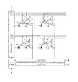
図12は、従来の固体撮像装置の概略構成を示すブロック図である。この構成例では、少なくとも、光を受光し信号を出力する画素アレイ1と、画素アレイ1を制御する垂直走査回路2と、画素から出力される信号を処理し、保持するノイズ抑圧回路4と、水平走査回路5により構成されている。なお、図12において、6は出力信号線に接続された出力アンプである。図13は、従来の固体撮像装置の具体的な構成を示す回路構成図であり、図14は、ローリングシャッタ機能を使用したときのノイズ抑圧回路の動作を説明するためのタイミングチャートである。また、図15は、グローバルシャッタ機能を使用したときのノイズ抑圧回路の動作を説明するためのタイミングチャートである。図16は、グローバルシャッタ機能時の光信号蓄積タイミングを説明するためのタイミングチャートである。また、図17は、ローリングシャッタ機能時の光信号蓄積タイミングを説明するためのタイミング図である。
FIG. 12 is a block diagram showing a schematic configuration of a conventional solid-state imaging device. In this configuration example, at least a
まず、図13を用いて従来の固体撮像装置の具体的な構成について説明する。まず画素の構成をPIX11を例に説明する。PIX11内には、光電変換部PD11と、光電変換部PD11で発生した信号を蓄積するメモリ(FD)C11と光電変換部PD11からメモリC11への転送を制御する転送スイッチMT11とメモリC11をリセットするリセットスイッチMR11と、メモリC11の信号を増幅する増幅部MA11と、画素を選択する選択スイッチMS11とが設けてあり、図13に示すように接続されており、複数の画素が2 次元に配置されて画素アレイを構成している。 First, a specific configuration of a conventional solid-state imaging device will be described with reference to FIG. First, the configuration of the pixel will be described by taking PIX11 as an example. In PIX11, the photoelectric conversion unit PD11, the memory (FD) C11 that accumulates signals generated in the photoelectric conversion unit PD11, the transfer switch MT11 that controls the transfer from the photoelectric conversion unit PD11 to the memory C11, and the memory C11 are reset. A reset switch MR11, an amplifying unit MA11 for amplifying a signal of the memory C11, and a selection switch MS11 for selecting a pixel are provided and connected as shown in FIG. 13, and a plurality of pixels are arranged two-dimensionally. The pixel array is configured.
また、転送スイッチMT11は、転送制御信号φTR1にて制御される。リセットスイッチMR11は、リセット制御信号φRS1にて制御される。選択スイッチMS11は選択制御信号φSEL1によって制御され、選択された画素行の信号はノイズ抑圧回路4へ出力する。ノイズ抑圧回路4では、画素のリセットバラツキを除去した値を保持する。その後ノイズ抑圧回路4に保持された信号は、水平走査回路5によって読み出され、出力信号線と出力アンプ6を介して出力される。なお、図13において、7は画素電源、I41(I42,I43)は垂直信号線に接続されているバイアス用電流源である。
The transfer switch MT11 is controlled by a transfer control signal φTR1. The reset switch MR11 is controlled by a reset control signal φRS1. The selection switch MS11 is controlled by a selection control signal φSEL1, and the signal of the selected pixel row is output to the noise suppression circuit 4. The noise suppression circuit 4 holds a value from which the pixel reset variation is removed. Thereafter, the signal held in the noise suppression circuit 4 is read out by the
このように構成されている固体撮像素装置においてローリングシャッタ機能を使用したときの光信号の蓄積タイミングについて、図17に示すタイミングチャートを用いて説明する。まず初めに、転送制御信号φTR1とリセット制御信号φRS1をハイレベルとすることで、両制御信号φTR1,φRS1で制御される行(1行目)の画素の光電変換部PDをリセットし、転送制御信号φTR1とリセット制御信号φRS1をロウレベルとすることで光信号の蓄積を開始する。その後、転送制御信号φTR2とリセット制御信号φRS2をハイレベルとすることで、両制御信号φTR2,φRS2にて制御される行(2行目)の光電変換部PDのリセットを行い、転送制御信号φTR2とリセット制御信号φRS2をロウレベルとすることで光信号の蓄積を開始する。 The accumulation timing of the optical signal when the rolling shutter function is used in the solid-state imaging device configured as described above will be described with reference to the timing chart shown in FIG. First, by setting the transfer control signal φTR1 and the reset control signal φRS1 to high level, the photoelectric conversion units PD of the pixels in the row (first row) controlled by both control signals φTR1 and φRS1 are reset, and transfer control is performed. The accumulation of the optical signal is started by setting the signal φTR1 and the reset control signal φRS1 to the low level. Thereafter, the transfer control signal φTR2 and the reset control signal φRS2 are set to a high level to reset the photoelectric conversion units PD in the row (second row) controlled by both control signals φTR2 and φRS2, and the transfer control signal φTR2 Then, the storage of the optical signal is started by setting the reset control signal φRS2 to the low level.
同様に、3行目以降の各行の転送制御信号とリセット制御信号を駆動することで各行の光電変換部PDが光信号の蓄積を開始する。光信号の蓄積を開始して所定の時間がたったのち、選択制御信号により制御される行の画素信号の出力を行う。まず、選択制御信号φSEL1をハイレベルとし、行(1行目)の選択を行う。次に、リセット制御信号φRS1をハイレベルとしてメモリ(FD)のリセットを行い、ロウレベルとすることでメモリ(FD)のリセットを終了する。このとき、画素からは、リセット信号が出力される。その後、転送制御信号φTR1をハイレベルとし、光電変換部PDに蓄積された光信号をメモリ(FD)へ転送し、転送制御信号φTR1をロウレベルとすることで、転送を終了する。このとき、画素からは、光信号が出力される。最後に選択制御信号φSEL1をロウレベルとすることで、選択された第1行目の画素信号読み出しを終了する。 Similarly, by driving the transfer control signal and the reset control signal in each row after the third row, the photoelectric conversion units PD in each row start storing optical signals. After a predetermined time has elapsed since the start of the accumulation of optical signals, the pixel signals of the rows controlled by the selection control signal are output. First, the selection control signal φSEL1 is set to a high level to select a row (first row). Next, the reset control signal φRS1 is set to the high level to reset the memory (FD), and the reset to the low level ends the resetting of the memory (FD). At this time, a reset signal is output from the pixel. Thereafter, the transfer control signal φTR1 is set to the high level, the optical signal stored in the photoelectric conversion unit PD is transferred to the memory (FD), and the transfer control signal φTR1 is set to the low level to complete the transfer. At this time, an optical signal is output from the pixel. Finally, the selection control signal φSEL1 is set to the low level, thereby completing the pixel signal reading of the selected first row.
次に、選択制御信号φSEL2にて選択される行(2行目)の読み出しを行う。この動作については、第1行目の動作と同じなので説明は省略する。以上の動作では、各行により光信号の蓄積開始時間と終了時間が異なる。 Next, the row selected by the selection control signal φSEL2 (second row) is read. Since this operation is the same as the operation in the first row, description thereof is omitted. In the above operation, the optical signal accumulation start time and end time are different for each row.
次に、グローバルシャッタ機能を使用したときの光信号の蓄積タイミングについて図16に示すタイミングチャートを用いて説明する。まず初めに、全ての行の転送制御信号φTR1,TR2,TR3,・・・、及び全ての行のリセット制御信号φRS1,RS2,RS3,・・・を同時にハイレベルとすることで、全画素の光電変換部PDを一括してリセットを行い、その後転送制御信号及びリセット制御信号をロウレベルにすることで、光信号の蓄積を開始する。所定の時間が経った後、全ての行の転送制御信号φTR1,TR2,TR3,・・・をハイレベルとすることで、光電変換部PDに蓄積された光信号を全画素一括してメモリ(FD)へ転送し、光信号の蓄積を終了する。 Next, optical signal accumulation timing when the global shutter function is used will be described with reference to a timing chart shown in FIG. First, the transfer control signals φTR1, TR2, TR3,... Of all rows and the reset control signals φRS1, RS2, RS3,. The photoelectric conversion unit PD is collectively reset, and then the transfer control signal and the reset control signal are set to the low level to start accumulation of the optical signal. After a predetermined time has passed, the transfer control signals φTR1, TR2, TR3,... Of all the rows are set to a high level, whereby the optical signals accumulated in the photoelectric conversion unit PD are collectively stored in the memory ( FD) and the accumulation of optical signals is terminated.
次に、選択制御信号により選択された行の画素信号出力を行う。まず選択制御信号φSEL1をハイレベルとし第1行目の画素の選択を行い、光信号の出力を行う。次に、リセット制御信号φRS1をハイレベルとすることでメモリ(FD)のリセットを行い、ロウレベルとすることでメモリ(FD)のリセットを終了する。このとき画素からは、リセット信号が出力される。最後に、選択制御信号φSEL1をロウレベルとすることで、第1行目の画素信号出力を終了する。その後、選択制御信号φSEL2にて選択される行(2行目)の画素信号出力を開始する。以下同様にして、3行目以降の画素信号の出力を行う。以上の動作では、各行の光信号蓄積開始時間と終了時間は同じとなる。 Next, the pixel signal of the row selected by the selection control signal is output. First, the selection control signal φSEL1 is set to a high level to select a pixel in the first row, and an optical signal is output. Next, the memory (FD) is reset by setting the reset control signal φRS1 to a high level, and the reset of the memory (FD) is ended by setting the reset control signal φRS1 to a low level. At this time, a reset signal is output from the pixel. Finally, by setting the selection control signal φSEL1 to the low level, the pixel signal output of the first row is finished. Thereafter, the pixel signal output of the row (second row) selected by the selection control signal φSEL2 is started. In the same manner, pixel signals from the third row are output. In the above operation, the optical signal accumulation start time and end time of each row are the same.
次に、ローリングシャッタ機能を使用したときのノイズ抑圧回路の動作を、図14に示すタイミングチャートを用いて説明する。まず画素の動作について説明する。選択制御信号φSEL1をハイレベルとすることで画素信号を読み出す行(1行目)の選択を行う。光電変換部PDからの光信号の読み出しに先立ってリセット制御信号φRS1をハイレベルとしメモリ(FD)のリセットを行い、リセット制御信号φRS1をロウレベルとすることでメモリ(FD)のリセットを終了し、画素のリセット信号Vr をノイズ抑圧回路4へ出力する。次に、転送制御信号φTR1をハイレベルとし、光電変換部PDで蓄積された信号をメモリ(FD)へ転送し、リセット信号Vr に光信号Vs が重畳された信号(Vr +Vs )を画素からノイズ抑圧回路4へ出力する。最後に、選択制御信号φSEL1をロウレベルとすることで画素信号の読み出しを終了する。 Next, the operation of the noise suppression circuit when the rolling shutter function is used will be described using the timing chart shown in FIG. First, the operation of the pixel will be described. The row from which the pixel signal is read (first row) is selected by setting the selection control signal φSEL1 to the high level. Prior to reading the optical signal from the photoelectric conversion unit PD, the reset control signal φRS1 is set to a high level to reset the memory (FD), and the reset control signal φRS1 is set to a low level to end the resetting of the memory (FD). The pixel reset signal Vr is output to the noise suppression circuit 4. Next, the transfer control signal φTR1 is set to the high level, the signal accumulated in the photoelectric conversion unit PD is transferred to the memory (FD), and the signal (Vr + Vs) in which the optical signal Vs is superimposed on the reset signal Vr is noise from the pixel. Output to the suppression circuit 4. Finally, the pixel signal readout is completed by setting the selection control signal φSEL1 to the low level.
次に、画素から出力された信号を処理するノイズ抑圧回路4の動作を、画素PIX11の画素信号に注目して説明する。サンプルホールド制御信号φSHとクランプ制御信号φCLをハイレベルとし、ノイズ抑圧回路4のノードN2をクランプ電圧(Vref)8でクランプする。このとき画素からリセット信号Vr がノイズ抑圧回路4へ入力され、リセット信号Vr をクランプ容量CCL1でサンプリングする。クランプ制御信号φCLをロウレベルとすることで、リセット信号Vr のサンプリングを終了する。 Next, the operation of the noise suppression circuit 4 that processes the signal output from the pixel will be described by paying attention to the pixel signal of the pixel PIX11. The sample hold control signal φSH and the clamp control signal φCL are set to the high level, and the node N2 of the noise suppression circuit 4 is clamped with the clamp voltage (Vref) 8. At this time, the reset signal Vr is input from the pixel to the noise suppression circuit 4, and the reset signal Vr is sampled by the clamp capacitor CCL1. By setting the clamp control signal φCL to the low level, the sampling of the reset signal Vr is completed.
その後、画素からリセット信号Vr に光信号Vs が重畳された信号(Vr +Vs )が、ノイズ抑圧回路4へ入力される。そのときノイズ抑圧回路4のノードN2は、先のサンプリングされたリセット信号Vr と画素から入力された(Vr +Vs )信号との差分信号Vs を、クランプ容量CCL1とサンプリング容量CSH1とで決まるゲインG倍した電圧GVs となる。その後、サンプルホールド制御信号φSHをロウレベルとすることで、ノードN2の電圧GVs を保持する。なお、ゲインGは、次式で表される。
G=CCL1/(CCL1+CSH1)
以上の動作を行うことで、光電変換部PDで蓄積された光信号を増幅した信号GVs を出力することが可能となる。
Thereafter, a signal (Vr + Vs) in which the optical signal Vs is superimposed on the reset signal Vr from the pixel is input to the noise suppression circuit 4. At that time, the node N2 of the noise suppression circuit 4 uses a gain G times determined by the clamp capacitor CCL1 and the sampling capacitor CSH1 for the difference signal Vs between the previously sampled reset signal Vr and the (Vr + Vs) signal input from the pixel. Voltage GVs. Thereafter, the voltage GVs at the node N2 is held by setting the sample hold control signal φSH to the low level. The gain G is expressed by the following equation.
G = CCL1 / (CCL1 + CSH1)
By performing the above operation, it is possible to output a signal GVs obtained by amplifying the optical signal accumulated in the photoelectric conversion unit PD.
次に、グローバルシャッタ機能を使用したときのノイズ抑圧回路4の動作を、図15に示すタイミングチャートを用いて説明する。まず画素の動作について説明する。転送制御信号φTR1をハイレベルとすることで、光電変換部PDに蓄積された信号をメモリ(FD)へ転送する。このときメモリ(FD)では、リセット信号と光信号が重畳された信号を保持する。 Next, the operation of the noise suppression circuit 4 when the global shutter function is used will be described using the timing chart shown in FIG. First, the operation of the pixel will be described. By setting the transfer control signal φTR1 to the high level, the signal accumulated in the photoelectric conversion unit PD is transferred to the memory (FD). At this time, the memory (FD) holds a signal in which the reset signal and the optical signal are superimposed.
次に、選択制御信号φSEL1をハイレベルとすることで、画素信号を読み出す行(1行目)の選択を行い、リセット信号Vr と光信号Vs が重畳された信号(Vr +Vs )を画素から出力する。その後、リセット制御信号φRS1をハイレベルとしメモリ(FD)のリセットを行い、リセット制御信号φRS1をロウレベルとすることで、メモリ(FD)のリセットを終了し、画素のリセット信号Vr をノイズ抑圧回路4へ出力する。最後に選択制御信号φSEL1をロウレベルとすることで、画素信号の読み出しを終了する。 Next, the selection control signal φSEL1 is set to the high level to select the row from which the pixel signal is read (first row), and the signal (Vr + Vs) in which the reset signal Vr and the optical signal Vs are superimposed is output from the pixel. To do. Thereafter, the reset control signal φRS1 is set to the high level to reset the memory (FD), and the reset control signal φRS1 is set to the low level to complete the resetting of the memory (FD), and the pixel reset signal Vr is used as the noise suppression circuit 4. Output to. Finally, the selection control signal φSEL1 is set to the low level to complete the reading of the pixel signal.
次に、画素から出力された信号を処理するノイズ抑圧回路4の動作を説明する。サンプルホールド制御信号φSHとクランプ制御信号φCLをハイレベルとし、ノイズ抑圧回路4のノードN2がクランプ電圧(Vref)8でクランプされる。このとき画素からリセット信号Vr と光信号Vs が重畳された信号(Vr +Vs )がノイズ抑圧回路4へ入力され、(Vr +Vs )をクランプ容量CCL1でサンプリングする。クランプ制御信号φCLをロウレベルとすることで、サンプリングを終了する。 Next, the operation of the noise suppression circuit 4 that processes signals output from the pixels will be described. The sample hold control signal φSH and the clamp control signal φCL are set to the high level, and the node N2 of the noise suppression circuit 4 is clamped by the clamp voltage (Vref) 8. At this time, a signal (Vr + Vs) in which the reset signal Vr and the optical signal Vs are superimposed is input from the pixel to the noise suppression circuit 4, and (Vr + Vs) is sampled by the clamp capacitor CCL1. Sampling is terminated by setting the clamp control signal φCL to a low level.
その後、画素からリセット信号Vr がノイズ抑圧回路4へ入力される。そのとき、ノイズ抑圧回路4のノードN2は、先のサンプリングされた信号(Vr +Vs )と画素から入力されたリセット信号Vr との差分である信号−Vs を、クランプ容量CCL1とサンプリング容量CSH1とで決まるゲインG倍した電圧−GVs となる。その後、サンプルホールド制御信号φSHをロウレベルとすることで、ノードN2の電圧−GVs を保持する。以上の動作を行うことで、光電変換部PDで蓄積された光信号を増幅した信号−GVs を出力することが可能となる。上記の動作を行うことで光信号を読み出すことが可能である。
しかし、上記従来例のノイズ抑圧回路の出力は、ローリングシャッタ動作時の出力GVs とグローバルシャッタ動作時の出力−GVs とで極性が反転する。このため、ノイズ抑圧回路の出力ダイナミックレンジが増大することにより、回路が大型化し、消費電力が増大する。本発明は、従来の固体撮像装置における上記課題を解決するためになされたものであり、読み出し動作を切り換えた場合でもノイズ抑圧回路の出力の極性を統一し、回路の小型化及び低消費電力化を図った固体撮像装置を提供することを目的としている。 However, the polarity of the output of the conventional noise suppression circuit is inverted between the output GVs during the rolling shutter operation and the output -GVs during the global shutter operation. For this reason, when the output dynamic range of the noise suppression circuit increases, the circuit becomes larger and the power consumption increases. The present invention has been made to solve the above-mentioned problems in the conventional solid-state imaging device, and even when the readout operation is switched, the polarity of the output of the noise suppression circuit is unified, and the circuit is downsized and the power consumption is reduced. An object of the present invention is to provide a solid-state imaging device that achieves the above.
上記課題を解決するため、請求項1に係る発明は、光電変換を行う光電変換部と、前記光電変換部で発生した信号を一時的に記憶しておくための蓄積部と、前記光電変換部の信号を前記蓄積部へ転送する転送手段と、前記蓄積部をリセットするリセット手段と、前記蓄積部の電位を増幅して出力する増幅手段と、前記増幅手段を選択する選択手段とを有する画素を2次元に複数配置されてなる画素部と、画素に起因する特性の異なる第1の信号と第2の信号との差分の極性を切り換える切り換え部を有し、画素毎のリセット時の信号のばらつきを抑圧するノイズ抑圧回路と、前記蓄積部をリセットした後、第1の信号としてリセット信号を前記画素から出力させ、その後前記光電変換部で発生した信号を前記蓄積部へ転送し、第2の信号として出力させる第1の読み出しモードと、前記蓄積部をリセットし、その後、前記光電変換部で発生した信号を前記蓄積部へ転送し、第1の信号として前記画素から出力させた後、前記蓄積部のリセットを行い、第2の信号としてリセット信号を前記画素から出力する第2の読み出しモードとを設定するモード設定部とを有し、前記切り換え部は、前記モード設定部で設定されたモードに応じて極性の切り換えを実行し、前記第2の読み出しモードが設定されたときには、前記転送手段は、前記光電変換部で発生した信号を全画素一括して蓄積部に転送するよう制御され、前記ノイズ抑圧回路は、前記画素に接続されたクランプ容量と該クランプ容量に接続されたサンプリング容量を有し、第1の期間に前記第1の信号を前記クランプ容量にサンプリングし、第2の期間に前記第2の信号と前記第1の信号の差を所定のゲイン倍した差分信号を前記サンプリング容量に発生させ、前記切り換え部は、前記第1の読み出しモード及び前記第2の読み出しモードのいずれか一方において、前記第2の期間に前記サンプリング容量に前記差分信号が出力されるように接続し、前記第1の読み出しモード及び前記第2の読み出しモードのいずれか他方において、前記第2の期間の後に、前記サンプリング容量に保持されている前記差分信号の極性を逆にして読み出すように固体撮像装置を構成するものである。
In order to solve the above problems, the invention according to
請求項2に係る発明は、請求項1に係る固体撮像装置において、前記ノイズ抑圧回路のアナログ出力信号をデジタル信号に変換するアナログデジタル変換器を更に備えることを特徴とするものである。
The invention according to
本発明によれば、ノイズ抑圧回路は画素に起因する特性の異なる第1及び第2の信号の差分の極性を切り換える切り換え部を有しているので、読み出しモードを切り換えた場合でも、ノイズ抑圧回路の出力の極性を統一することができ、回路の小型化及び低消費電力化を図ることができる。 According to the present invention, since the noise suppression circuit has the switching unit that switches the polarity of the difference between the first and second signals having different characteristics due to the pixels, the noise suppression circuit even when the readout mode is switched. The output polarity can be unified, and the circuit can be reduced in size and power consumption.
次に、本発明を実施するための最良の形態について説明する。 Next, the best mode for carrying out the present invention will be described.
(実施例1)
まず、本発明に係る固体撮像装置の実施例1について説明する。図1は、実施例1に係る固体撮像装置の概略構成を示すブロック図で、図12に示した従来例と対応する部分には同一符号を付して示している。この実施例1に係る固体撮像装置は、少なくとも、光を受光し信号を出力する画素アレイ1と、画素アレイ1を制御する垂直走査回路2と、モード設定部3と、モード設定部3により選択されるモードにより極性の制御を行い、画素から出力される信号を処理し、保持するノイズ抑圧回路4と、水平走査回路5により構成される。なお、6は出力アンプであり、上記モード設定部3は垂直走査回路2の切り換え制御も行うようになっている。
Example 1
First,
図2は、実施例1に係る固体撮像装置におけるノイズ抑圧回路4の構成を示す回路図である。このノイズ抑圧回路4は、画素アレイ1の第1列目の出力V1に対して、クランプ容量CCL1とサンプリング容量CSH1と、サンプルホールドスイッチM11と、クランプスイッチM21,M31と、駆動スイッチM41,M51と、水平選択スイッチM6と、増幅器A1とが設けられており、図2に示すように接続されている。そして、画素アレイ1の他の列からの出力V2,V3に対しても同様の回路が接続されている。また、サンプルホールドスイッチM11はサンプルホールド制御信号φSHで制御され、クランプスイッチM21はクランプ制御信号φCL1で、クランプスイッチM31はクランプ制御信号φCL2で制御される。また駆動スイッチM41は駆動制御信号φSL1で、駆動スイッチM51は駆動制御信号φSL2で制御されるようになっている。
FIG. 2 is a circuit diagram illustrating a configuration of the noise suppression circuit 4 in the solid-state imaging device according to the first embodiment. The noise suppression circuit 4 includes a clamp capacitor CCL1, a sampling capacitor CSH1, a sample hold switch M11, clamp switches M21 and M31, and drive switches M41 and M51 for the output V1 in the first column of the
次に、このような構成のノイズ抑圧回路を備えた実施例1に係る固体撮像装置のローリングシャッタ機能を使用して光信号を読み出す動作を、図3に示すタイミングチャートを用いて説明する。画素の読み出し動作については、従来例と同じなので、その説明は省略し、ノイズ抑圧回路4の動作を画素アレイ1の1列目の出力V1に注目して説明する。まずクランプ制御信号φCL2と駆動制御信号φSL1はハイレベルに、駆動制御信号φSL2は、ロウレベルに設定される。次に、サンプルホールド制御信号φSHとクランプ制御信号φCL1をハイレベルとし、ノイズ抑圧回路4のノードN2,N3がクランプ電圧(Vref)8でクランプされる。このとき、画素からリセット信号Vr がノイズ抑圧回路4へ入力され、リセット信号Vr をクランプ容量CCL1でサンプリングを行う。クランプ制御信号φCL1をロウレベルとすることで、リセット信号Vr のサンプリングを終了する。
Next, an operation of reading an optical signal using the rolling shutter function of the solid-state imaging device according to the first embodiment provided with the noise suppression circuit having such a configuration will be described with reference to a timing chart shown in FIG. Since the pixel reading operation is the same as in the conventional example, the description thereof is omitted, and the operation of the noise suppression circuit 4 will be described by paying attention to the output V1 in the first column of the
その後、画素からリセット信号Vr に光信号Vs が重畳された信号(Vr +Vs )がノイズ抑圧回路4へ入力される。そのとき、ノイズ抑圧回路4のノードN2は、先のサンプリングされたリセット信号Vr と画素から入力された(Vr +Vs )信号との差分である信号Vs を、クランプ容量CCL1とサンプリング容量CSH1とで決まるゲインG倍した電圧GVs となる。その後、サンプルホールド制御信号φSHをロウレベルとすることで、ノードN2の電圧GVs を保持する。よって、ノードN4は、ノードN2と同じ電圧GVs を出力することが可能となる。以上の動作を行うことで、光電変換部PDで蓄積された光信号を増幅した信号GVs を出力することが可能となる。 Thereafter, a signal (Vr + Vs) in which the optical signal Vs is superimposed on the reset signal Vr is input from the pixel to the noise suppression circuit 4. At that time, the node N2 of the noise suppression circuit 4 determines the signal Vs, which is the difference between the previously sampled reset signal Vr and the (Vr + Vs) signal input from the pixel, by the clamp capacitor CCL1 and the sampling capacitor CSH1. The voltage GVs is multiplied by the gain G. Thereafter, the voltage GVs at the node N2 is held by setting the sample hold control signal φSH to the low level. Therefore, the node N4 can output the same voltage GVs as the node N2. By performing the above operation, it is possible to output a signal GVs obtained by amplifying the optical signal accumulated in the photoelectric conversion unit PD.
次に、グローバルシャッタ機能を使用して光信号を読み出す動作を、図4に示すタイミングチャートを用いて説明する。画素の読み出し動作については、従来例と同じなので説明は省略し、ノイズ抑圧回路4の動作について説明する。まず駆動制御信号φSL2はハイレベルに、駆動制御信号φSL1は、ロウレベルに設定される。 Next, an operation of reading an optical signal using the global shutter function will be described with reference to a timing chart shown in FIG. Since the pixel reading operation is the same as that of the conventional example, the description thereof will be omitted, and the operation of the noise suppression circuit 4 will be described. First, the drive control signal φSL2 is set to a high level, and the drive control signal φSL1 is set to a low level.
次に、サンプルホールド制御信号φSHとクランプ制御信号φCL1,φCL2をハイレベルとし、ノイズ抑圧回路4のノードN2,N3がクランプ電圧8でクランプされる。このとき、画素からはリセット信号Vr に光信号Vs が重畳された信号(Vr +Vs )がノイズ抑圧回路4へ入力され、信号(Vr +Vs )をクランプ容量CCL1でサンプリングする。クランプ制御信号φCL1をロウレベルとすることで、信号(Vr +Vs )のサンプリングを終了する。
Next, the sample hold control signal φSH and the clamp control signals φCL1 and φCL2 are set to the high level, and the nodes N2 and N3 of the noise suppression circuit 4 are clamped by the
その後、画素からリセット信号Vr がノイズ抑圧回路4へ入力され, ノイズ抑圧回路4のノードN2は、先のサンプリングされた信号(Vr +Vs )と画素から入力された信号Vr との差分である信号−Vs を、クランプ容量CCL1とサンプリング容量CSH1とで決まるゲインG倍した電圧−GVs となる。その後、サンプルホールド制御信号φSHをロウレベルとすることでサンプリングを終了する。そして、クランプ制御信号φCL2をロウレベルに、φCL1をハイレベルにする。ノードN2がクランプ電圧8となり、ノードN3の電圧は、ノードN2の電圧変動分GVs を保持する。よって、ノードN4の電圧は、ノードN2と同じGVs となる。
Thereafter, the reset signal Vr is input from the pixel to the noise suppression circuit 4, and the node N2 of the noise suppression circuit 4 is a signal − that is the difference between the previously sampled signal (Vr + Vs) and the signal Vr input from the pixel. The voltage −GVs is obtained by multiplying Vs by a gain G determined by the clamp capacitor CCL1 and the sampling capacitor CSH1. Thereafter, the sampling is finished by setting the sample hold control signal φSH to the low level. Then, the clamp control signal φCL2 is set to the low level and φCL1 is set to the high level. The node N2 becomes the
以上の動作を行うことで、モード設定部3によりローリングシャッタ機能とグローバルシャッタ機能の動作を切り換えた場合でも、ノイズ抑圧回路4の出力信号の極性が統一され、回路の小型化及び低消費電力化を図ることができる。また、画素アレイがグローバルシャッタ動作時に、ノイズ抑圧回路4を上記ローリングシャッタ駆動とし、画素アレイがローリングシャッタ動作時にノイズ抑圧回路4を上記グローバルシャッタ駆動とすることも可能である。
By performing the above operation, the polarity of the output signal of the noise suppression circuit 4 is unified even when the operation of the rolling shutter function and the global shutter function is switched by the
(実施例2)
次に、実施例2について説明する。図5は、実施例2に係る固体撮像装置のノイズ抑圧回路4の構成を示す回路図である。この実施例に係るノイズ抑圧回路4は、画素アレイ1の第1列目の出力V1に対して、クランプ容量CCL1,CCR1と、帰還容量CRA1と、サンプリング容量CSH1と、サンプルホールドスイッチM11と、クランプスイッチM21,M31,M71と、駆動スイッチM41,M51と、帰還スイッチM81と、帰還増幅器A1と、水平選択スイッチM61とが設けられており、図5に示すように接続されている。画素アレイの他の列からの出力V2,V3に対しても同様の回路が接続されている。
(Example 2)
Next, Example 2 will be described. FIG. 5 is a circuit diagram illustrating a configuration of the noise suppression circuit 4 of the solid-state imaging device according to the second embodiment. The noise suppression circuit 4 according to this embodiment has a clamp capacitor CCL1, CCR1, a feedback capacitor CRA1, a sampling capacitor CSH1, a sample hold switch M11, a clamp for the output V1 of the first column of the
また、サンプルホールドスイッチM11はサンプルホールド制御信号φSHで制御され、クランプスイッチM21はクランプ制御信号φCL1で、クランプスイッチM31はクランプ制御信号φCL2で, クランプスイッチM71はクランプ制御信号φCL3で制御される。駆動スイッチM41は駆動制御信号φSL1で、駆動スイッチM51は駆動制御信号φSL2で制御される。帰還スイッチM81は帰還制御信号φRAで制御されるようになっている。 The sample hold switch M11 is controlled by a sample hold control signal φSH, the clamp switch M21 is controlled by a clamp control signal φCL1, the clamp switch M31 is controlled by a clamp control signal φCL2, and the clamp switch M71 is controlled by a clamp control signal φCL3. The drive switch M41 is controlled by a drive control signal φSL1, and the drive switch M51 is controlled by a drive control signal φSL2. The feedback switch M81 is controlled by a feedback control signal φRA.
次に、このような構成のノイズ抑圧回路を備えた実施例2に係る固体撮像装置のローリングシャッタ機能を使用して光信号を読み出す動作を図6に示すタイミングチャートを用いて説明する。画素の読み出し動作については、従来例と同じなので、その説明は省略し、ノイズ抑圧回路4の動作について説明する。まずクランプ制御信号φCL2と駆動制御信号φSL1はハイレベル、クランプ制御信号φCL1と駆動制御信号φSL2は、ロウレベルに設定され、ノードN3は、クランプ電圧(Vref)8に設定される。 Next, an operation of reading an optical signal using the rolling shutter function of the solid-state imaging device according to the second embodiment having the noise suppression circuit having the above configuration will be described with reference to a timing chart shown in FIG. Since the pixel readout operation is the same as that in the conventional example, the description thereof is omitted, and the operation of the noise suppression circuit 4 will be described. First, the clamp control signal φCL2 and the drive control signal φSL1 are set to the high level, the clamp control signal φCL1 and the drive control signal φSL2 are set to the low level, and the node N3 is set to the clamp voltage (Vref) 8.
次に、サンプルホールド制御信号φSHとクランプ制御信号φCL3をハイレベルとし、ノイズ抑圧回路4のノードN2がクランプ電圧8でクランプされ、帰還制御信号φRAをハイレベルとすることで帰還容量CRA1をリセットする。このとき画素からリセット信号Vr がノイズ抑圧回路4へ入力され、リセット信号Vr をクランプ容量CCL1でサンプリングする。クランプ制御信号φCL1をロウレベルとすることで、リセット信号Vr のサンプリングを終了し、帰還制御信号φRAをロウレベルとすることで、帰還容量CRA1のリセットを終了する。
Next, the sample hold control signal φSH and the clamp control signal φCL3 are set to the high level, the node N2 of the noise suppression circuit 4 is clamped by the
その後、画素からリセット信号Vr に光信号Vs が重畳された信号(Vr +Vs )がノイズ抑圧回路4へ入力される。そのとき、ノイズ抑圧回路4のノードN2は、先のサンプリングされたリセット信号Vr と画素から入力された(Vr +Vs )信号との差分である信号Vs となる。また、帰還増幅器A1の出力であるノードN4は、ノードN2の信号Vs をクランプ容量CCR1と帰還容量CRA1とで決まるゲインG倍した電圧GVs となる。その後、サンプルホールド制御信号φSHをロウレベルとすることで、出力電圧GVs を保持する。 Thereafter, a signal (Vr + Vs) in which the optical signal Vs is superimposed on the reset signal Vr is input from the pixel to the noise suppression circuit 4. At that time, the node N2 of the noise suppression circuit 4 becomes a signal Vs which is a difference between the previously sampled reset signal Vr and the (Vr + Vs) signal input from the pixel. The node N4 that is the output of the feedback amplifier A1 becomes a voltage GVs obtained by multiplying the signal Vs of the node N2 by a gain G determined by the clamp capacitor CCR1 and the feedback capacitor CRA1. Thereafter, the output voltage GVs is held by setting the sample hold control signal φSH to the low level.
以上の動作を行うことで、光電変換部PDで蓄積された光信号を増幅した信号GVs を出力することが可能となる。なお、ゲインGは、次式で表される。
G=CRA1/CCR1
By performing the above operation, it is possible to output a signal GVs obtained by amplifying the optical signal accumulated in the photoelectric conversion unit PD. The gain G is expressed by the following equation.
G = CRA1 / CCR1
次に、グローバルシャッタ機能を使用して光信号を読み出す動作を、図7に示すタイミングチャートを用いて説明する。画素の読み出し動作については、従来例と同じなので説明は省略し、ノイズ抑圧回路4の動作について説明する。クランプ制御信号φCL1,φCL3と駆動制御信号φSL2はハイレベルに設定され、クランプ制御信号φCL2と駆動制御信号φSL1はロウレベルに設定され、ノードN1,N2はクランプ電圧(Vref)8に設定され、画素の出力はノードN3に入力されるようになっている。 Next, an operation of reading an optical signal using the global shutter function will be described with reference to a timing chart shown in FIG. Since the pixel reading operation is the same as that of the conventional example, the description thereof will be omitted, and the operation of the noise suppression circuit 4 will be described. The clamp control signals φCL1 and φCL3 and the drive control signal φSL2 are set to a high level, the clamp control signal φCL2 and the drive control signal φSL1 are set to a low level, the nodes N1 and N2 are set to a clamp voltage (Vref) 8, and The output is input to the node N3.
次に、サンプルホールド制御信号φSHと帰還制御信号φRAをハイレベルとし、帰還容量CRA1のリセットを行う。このとき、画素からリセット信号Vr に光信号Vs が重畳された信号(Vr +Vs )がノイズ抑圧回路4へ入力され、信号(Vr +Vs )をクランプ容量CCR1でサンプリングする。帰還制御信号φRAをロウレベルとすることで、帰還容量CRA1のリセット、及び信号(Vr +Vs )のサンプリングを終了する。 Next, the sample hold control signal φSH and the feedback control signal φRA are set to the high level, and the feedback capacitor CRA1 is reset. At this time, a signal (Vr + Vs) in which the optical signal Vs is superimposed on the reset signal Vr from the pixel is input to the noise suppression circuit 4, and the signal (Vr + Vs) is sampled by the clamp capacitor CCR1. By setting the feedback control signal φRA to the low level, the resetting of the feedback capacitor CRA1 and the sampling of the signal (Vr + Vs) are completed.
その後、画素からリセット信号Vr がノイズ抑圧回路4へ入力される。そのとき、帰還増幅器A1の出力であるノードN4は、先のサンプリングされた信号(Vr +Vs )とリセット信号Vr との差分である−Vs を、クランプ容量CCR1と帰還容量CRA1とで決まるゲイン−G倍した電圧GVs となる。その後、サンプルホールド制御信号φSHをロウレベルとすることで、出力電圧GVs を保持する。よって、光電変換部PDで蓄積された光信号を増幅した信号GVs を出力することが可能となる。 Thereafter, the reset signal Vr is input from the pixel to the noise suppression circuit 4. At this time, the node N4 which is the output of the feedback amplifier A1 has a gain −G determined by the clamp capacitor CCR1 and the feedback capacitor CRA1 as −Vs which is the difference between the previous sampled signal (Vr + Vs) and the reset signal Vr. The multiplied voltage GVs is obtained. Thereafter, the output voltage GVs is held by setting the sample hold control signal φSH to the low level. Therefore, it is possible to output the signal GVs obtained by amplifying the optical signal accumulated in the photoelectric conversion unit PD.
上記の回路構成及び上記動作を行うことで、モード設定部3によりローリングシャッタ機能とグローバルシャッタ機能とを切り換えた場合でも、ノイズ抑圧回路4の出力信号の極性が統一され、回路の小型化及び低消費電力化を図ることができる。また、画素アレイがグローバルシャッタ動作時に、ノイズ抑圧回路4を上記ローリングシャッタ駆動とし、画素アレイがローリングシャッタ動作時に、ノイズ抑圧回路4を上記グローバルシャッタ駆動とすることも可能である。
By performing the above circuit configuration and the above operation, the polarity of the output signal of the noise suppression circuit 4 is unified even when the rolling shutter function and the global shutter function are switched by the
(実施例3)
次に、実施例3について説明する。図8は、実施例3に係る固体撮像装置の画素構成を詳細に示す回路構成図である。この実施例に係る画素は、選択スイッチMS11,12,21,22と増幅部MA11,12,21,22の接続構成が、実施例1及び2における画素構成と異なっている。なお、その他の回路構成及び動作については、実施例1,2と同じなので説明は省略する。上記の回路構成とすることでローリングシャッタ機能とグローバルシャッタ機能とを切り換えた場合でも、ノイズ抑圧回路の出力信号の極性が統一され、回路の小型化及び低消費電力化図ることができる。
(Example 3)
Next, Example 3 will be described. FIG. 8 is a circuit configuration diagram illustrating in detail the pixel configuration of the solid-state imaging device according to the third embodiment. In the pixel according to this embodiment, the connection configuration of the selection switches MS11, 12, 21, and 22 and the amplification units MA11, 12, 21, and 22 is different from the pixel configuration in the first and second embodiments. Since other circuit configurations and operations are the same as those in the first and second embodiments, description thereof will be omitted. With the above circuit configuration, even when the rolling shutter function and the global shutter function are switched, the polarity of the output signal of the noise suppression circuit is unified, and the circuit can be reduced in size and power consumption.
(実施例4)
次に、実施例4について説明する。図9は、実施例4に係る固体撮像装置の画素構成を詳細に示す回路構成図である。この実施例は、画素構成が異なるのみで、他の構成は実施例1又は2と同じである。この実施例の画素構成をPIX11を例に説明する。PIX11内には、光電変換部PD11と、光電変換部PD11で発生した信号を蓄積するメモリ(FD)C11と、光電変換部PD11からメモリC11への転送を制御する転送スイッチMT11と、メモリC11をリセットするリセットスイッチMR11と、メモリC11の信号を増幅する増幅部MA11と、画素を選択する選択スイッチMS11と、光電変換部PDで発生した信号を排出する排出スイッチME11とが設けられており、図9に示すように接続されていて、2次元に配置されている。
Example 4
Next, Example 4 will be described. FIG. 9 is a circuit configuration diagram illustrating in detail a pixel configuration of the solid-state imaging apparatus according to the fourth embodiment. In this embodiment, only the pixel configuration is different, and other configurations are the same as those in the first or second embodiment. The pixel configuration of this embodiment will be described by taking PIX11 as an example. In PIX11, there are a photoelectric conversion unit PD11, a memory (FD) C11 for accumulating signals generated in the photoelectric conversion unit PD11, a transfer switch MT11 for controlling transfer from the photoelectric conversion unit PD11 to the memory C11, and a memory C11. A reset switch MR11 for resetting, an amplifying unit MA11 for amplifying the signal of the memory C11, a selection switch MS11 for selecting a pixel, and a discharge switch ME11 for discharging a signal generated in the photoelectric conversion unit PD are provided. 9 are connected in a two-dimensional manner.
また、転送スイッチMT11は転送制御信号φTX1にて制御され、リセットスイッチMR11はリセット制御信号φRST1にて制御され、排出スイッチME11は排出制御信号φRSP1で制御される。選択スイッチMS11は選択制御信号φSEL1によって制御され、選択された行(1行目)の信号はノイズ抑圧回路4へ出力される。ノイズ抑圧回路4では、画素のリセットバラツキを除去した値を保持する。その後ノイズ抑圧回路4に保持された信号は、水平走査回路5によって読み出される。
Further, the transfer switch MT11 is controlled by the transfer control signal φTX1, the reset switch MR11 is controlled by the reset control signal φRST1, and the discharge switch ME11 is controlled by the discharge control signal φRSP1. The selection switch MS11 is controlled by a selection control signal φSEL1, and the signal of the selected row (first row) is output to the noise suppression circuit 4. The noise suppression circuit 4 holds a value from which the pixel reset variation is removed. Thereafter, the signal held in the noise suppression circuit 4 is read out by the
上記画素構成の画素アレイを用いた場合においても、実施例1及び2に示したと同様にモード設定でローリングシャッタ機能とグローバルシャッタ機能とを切り換え設定することにより、ノイズ抑圧回路の出力信号の極性が統一され、回路の小型化及び低消費電力化を図ることができる。なお、この実施例の画素構成とした場合、グローバルシャッタ駆動時の蓄積時間をフレキシブルに設定できる。 Even when the pixel array having the above pixel configuration is used, the polarity of the output signal of the noise suppression circuit can be changed by switching between the rolling shutter function and the global shutter function by mode setting as in the first and second embodiments. The circuit can be unified and the circuit can be reduced in size and power consumption. In the case of the pixel configuration of this embodiment, the accumulation time when driving the global shutter can be set flexibly.
(実施例5)
次に、実施例5について説明する。図10は、実施例5に係る固体撮像装置の構成を示すブロック図である。この実施例は、実施例1,2に係る固体撮像装置において、ノイズ抑圧回路4の各列の出力にそれぞれアナログデジタル変換器(AD)10が配置された構成となっている。画素アレイ1及びノイズ抑圧回路4の構成は、実施例1,2と同じなので説明は省略する。また、画素動作及びノイズ抑圧回路4の駆動も実施例1,2と同じなので説明は省略する。
(Example 5)
Next, Example 5 will be described. FIG. 10 is a block diagram illustrating the configuration of the solid-state imaging device according to the fifth embodiment. In this embodiment, in the solid-state imaging device according to the first and second embodiments, an analog-digital converter (AD) 10 is arranged at the output of each column of the noise suppression circuit 4. Since the configurations of the
このような構成とすることで、モード設定部3によりローリングシャッタ機能とグローバルシャッタ機能とを切り換えた場合でも、AD変換器10を介して出力されるデジタル出力信号の極性が統一され、回路の小型化及び低消費電力化を図ることができる。
With this configuration, even when the
(実施例6)
次に、実施例6について説明する。図11は、実施例6に係る固体撮像装置の構成を示すブロック図である。この実施例は、実施例1,2に係る固体撮像装置において、ノイズ抑圧回路4の各列の出力が単一のアナログデジタル変換器11に接続されている構成となっている。画素構成及びノイズ抑圧回路4の構成は、実施例1,2と同じなので説明は省略する。また、画素動作及びノイズ抑圧回路4の駆動も実施例1,2と同じなので説明は省略する。
(Example 6)
Next, Example 6 will be described. FIG. 11 is a block diagram illustrating the configuration of the solid-state imaging device according to the sixth embodiment. In this embodiment, the output of each column of the noise suppression circuit 4 is connected to a single analog-
このような構成とすることで、モード設定部3によりローリングシャッタ機能とグローバルシャッタ機能とを切り換えた場合でも、単一のAD変換器11を介して出力されるデジタル出力信号の極性が統一され、回路の小型化及び低消費電力化を図ることができる。
With this configuration, even when the rolling shutter function and the global shutter function are switched by the
1 画素アレイ
2 垂直走査回路
3 モード設定部
4 ノイズ抑圧回路
5 水平走査回路
6 出力アンプ
7 画素電源
8 クランプ電圧
10,11 AD変換器
DESCRIPTION OF
10, 11 AD converter
Claims (2)
画素に起因する特性の異なる第1の信号と第2の信号との差分の極性を切り換える切り換え部を有し、画素毎のリセット時の信号のばらつきを抑圧するノイズ抑圧回路と、
前記蓄積部をリセットした後、第1の信号としてリセット信号を前記画素から出力させ、その後前記光電変換部で発生した信号を前記蓄積部へ転送し、第2の信号として出力させる第1の読み出しモードと、前記蓄積部をリセットし、その後、前記光電変換部で発生した信号を前記蓄積部へ転送し、第1の信号として前記画素から出力させた後、前記蓄積部のリセットを行い、第2の信号としてリセット信号を前記画素から出力する第2の読み出しモードとを設定するモード設定部とを有し、
前記切り換え部は、前記モード設定部で設定されたモードに応じて極性の切り換えを実行し、
前記第2の読み出しモードが設定されたときには、前記転送手段は、前記光電変換部で発生した信号を全画素一括して蓄積部に転送するよう制御され、
前記ノイズ抑圧回路は、前記画素に接続されたクランプ容量と該クランプ容量に接続されたサンプリング容量を有し、第1の期間に前記第1の信号を前記クランプ容量にサンプリングし、第2の期間に前記第2の信号と前記第1の信号の差を所定のゲイン倍した差分信号を前記サンプリング容量に発生させ、
前記切り換え部は、前記第1の読み出しモード及び前記第2の読み出しモードのいずれか一方において、前記第2の期間に前記サンプリング容量に前記差分信号が出力されるように接続し、前記第1の読み出しモード及び前記第2の読み出しモードのいずれか他方において、前記第2の期間の後に、前記サンプリング容量に保持されている前記差分信号の極性を逆にして読み出す、
ことを特徴とする固体撮像装置。 A photoelectric conversion unit that performs photoelectric conversion, a storage unit for temporarily storing a signal generated in the photoelectric conversion unit, a transfer unit that transfers a signal of the photoelectric conversion unit to the storage unit, and the storage A pixel unit formed by two-dimensionally arranging a pixel having a reset unit that resets the unit, an amplification unit that amplifies and outputs the potential of the storage unit, and a selection unit that selects the amplification unit;
A noise suppression circuit that includes a switching unit that switches a polarity of a difference between a first signal and a second signal having different characteristics due to pixels, and that suppresses variation in signals at the time of reset for each pixel;
After the storage unit is reset, a reset signal is output from the pixel as a first signal, and then a signal generated in the photoelectric conversion unit is transferred to the storage unit and output as a second signal. Reset the mode and the storage unit, and then transfer the signal generated in the photoelectric conversion unit to the storage unit, output from the pixel as the first signal, and then reset the storage unit, A mode setting unit for setting a second readout mode in which a reset signal is output from the pixel as a signal of 2;
The switching unit executes polarity switching according to the mode set by the mode setting unit,
When the second readout mode is set, the transfer means is controlled to transfer the signal generated by the photoelectric conversion unit to the accumulation unit collectively for all pixels,
The noise suppression circuit has a clamp capacitor connected to the pixel and a sampling capacitor connected to the clamp capacitor, and samples the first signal into the clamp capacitor in a first period, and a second period. A difference signal obtained by multiplying a difference between the second signal and the first signal by a predetermined gain is generated in the sampling capacitor,
The switching unit is connected so that the differential signal is output to the sampling capacitor in the second period in any one of the first readout mode and the second readout mode, and the first readout mode In either one of the readout mode and the second readout mode, after the second period , readout is performed with the polarity of the differential signal held in the sampling capacitor reversed .
A solid-state imaging device.
Priority Applications (2)
| Application Number | Priority Date | Filing Date | Title |
|---|---|---|---|
| JP2007096145A JP5412030B2 (en) | 2007-04-02 | 2007-04-02 | Solid-state imaging device |
| US12/060,591 US8102441B2 (en) | 2007-04-02 | 2008-04-01 | Solid-state imaging apparatus |
Applications Claiming Priority (1)
| Application Number | Priority Date | Filing Date | Title |
|---|---|---|---|
| JP2007096145A JP5412030B2 (en) | 2007-04-02 | 2007-04-02 | Solid-state imaging device |
Publications (3)
| Publication Number | Publication Date |
|---|---|
| JP2008258716A JP2008258716A (en) | 2008-10-23 |
| JP2008258716A5 JP2008258716A5 (en) | 2010-04-22 |
| JP5412030B2 true JP5412030B2 (en) | 2014-02-12 |
Family
ID=39793595
Family Applications (1)
| Application Number | Title | Priority Date | Filing Date |
|---|---|---|---|
| JP2007096145A Expired - Fee Related JP5412030B2 (en) | 2007-04-02 | 2007-04-02 | Solid-state imaging device |
Country Status (2)
| Country | Link |
|---|---|
| US (1) | US8102441B2 (en) |
| JP (1) | JP5412030B2 (en) |
Families Citing this family (7)
| Publication number | Priority date | Publication date | Assignee | Title |
|---|---|---|---|---|
| US7841533B2 (en) | 2003-11-13 | 2010-11-30 | Metrologic Instruments, Inc. | Method of capturing and processing digital images of an object within the field of view (FOV) of a hand-supportable digitial image capture and processing system |
| US7866557B2 (en) * | 2007-09-27 | 2011-01-11 | Symbol Technologies, Inc. | Imaging-based bar code reader utilizing modified rolling shutter operation |
| JP5098831B2 (en) * | 2008-06-06 | 2012-12-12 | ソニー株式会社 | Solid-state imaging device and camera system |
| JP5653597B2 (en) * | 2009-06-25 | 2015-01-14 | ソニー株式会社 | Solid-state imaging device and imaging device |
| JP5361628B2 (en) * | 2009-09-15 | 2013-12-04 | キヤノン株式会社 | Imaging apparatus and imaging system, control method thereof, and program thereof |
| CN102640017B (en) * | 2009-12-01 | 2015-02-11 | 佳能株式会社 | Image pickup device, image pickup system, control method therefor |
| DE112011100842T5 (en) | 2010-03-08 | 2013-01-17 | Semiconductor Energy Laboratory Co., Ltd. | Semiconductor component and method for its production |
Family Cites Families (7)
| Publication number | Priority date | Publication date | Assignee | Title |
|---|---|---|---|---|
| GB0020280D0 (en) * | 2000-08-18 | 2000-10-04 | Vlsi Vision Ltd | Modification of column fixed pattern column noise in solid image sensors |
| JP2002320141A (en) * | 2001-04-20 | 2002-10-31 | Canon Inc | Solid-state imaging device and imaging method |
| JP3894534B2 (en) * | 2001-05-16 | 2007-03-22 | キヤノン株式会社 | Imaging apparatus and radiation imaging apparatus |
| JP4299588B2 (en) * | 2003-05-29 | 2009-07-22 | 株式会社ルネサステクノロジ | Semiconductor integrated circuit device |
| JP2005210693A (en) * | 2003-12-25 | 2005-08-04 | Toshiba Corp | Solid-state imaging device, digital camera, and digital video camera |
| JP4442515B2 (en) * | 2005-06-02 | 2010-03-31 | ソニー株式会社 | Solid-state imaging device, analog-digital conversion method in solid-state imaging device, and imaging device |
| JP2007074435A (en) * | 2005-09-07 | 2007-03-22 | Funai Electric Co Ltd | Solid-state imaging device and its drive method |
-
2007
- 2007-04-02 JP JP2007096145A patent/JP5412030B2/en not_active Expired - Fee Related
-
2008
- 2008-04-01 US US12/060,591 patent/US8102441B2/en not_active Expired - Fee Related
Also Published As
| Publication number | Publication date |
|---|---|
| US8102441B2 (en) | 2012-01-24 |
| JP2008258716A (en) | 2008-10-23 |
| US20080239108A1 (en) | 2008-10-02 |
Similar Documents
| Publication | Publication Date | Title |
|---|---|---|
| JP4500862B2 (en) | Driving method of solid-state imaging device | |
| JP5264379B2 (en) | IMAGING DEVICE, IMAGING SYSTEM, AND OPERATION METHOD OF IMAGING DEVICE | |
| JP4929075B2 (en) | Solid-state imaging device, driving method thereof, and imaging device | |
| JP5412030B2 (en) | Solid-state imaging device | |
| JP6377947B2 (en) | Solid-state imaging device and electronic device | |
| US20050264666A1 (en) | Image pickup device for reducing shading in vertical direction under long-term exposure | |
| JP2008258716A5 (en) | ||
| JP2008271186A (en) | Solid-state imaging apparatus | |
| JP2009260428A (en) | Solid-state imaging device | |
| US8094220B2 (en) | Solid-state imaging apparatus and driving method of solid-state imaging apparatus | |
| JP4337177B2 (en) | Solid-state imaging device and driving method thereof | |
| JP5721518B2 (en) | Imaging device and imaging apparatus | |
| CN108282601B (en) | Image sensor and image pickup apparatus | |
| JP5059669B2 (en) | Solid-state imaging device | |
| JP2008017100A (en) | Solid-state imaging device | |
| JP2007243731A (en) | Shift register, solid-state imaging element and control method | |
| JP2018182458A (en) | Signal processing apparatus and method, imaging element, and imaging apparatus | |
| JP2008300898A (en) | Solid state imaging device and imaging system employing it | |
| JP6049304B2 (en) | Solid-state imaging device and imaging device | |
| JP5098502B2 (en) | Solid-state imaging device | |
| JP5854652B2 (en) | Imaging device | |
| JP6765805B2 (en) | Image pickup device drive method, image pickup device, image pickup system | |
| JP5253280B2 (en) | Solid-state imaging device, camera system, and signal readout method | |
| JP2011087125A (en) | Solid-state imaging element | |
| JP7330739B2 (en) | IMAGING DEVICE, IMAGING DEVICE CONTROL METHOD, COMPUTER PROGRAM, AND STORAGE MEDIUM |
Legal Events
| Date | Code | Title | Description |
|---|---|---|---|
| A521 | Request for written amendment filed |
Free format text: JAPANESE INTERMEDIATE CODE: A523 Effective date: 20100304 |
|
| A621 | Written request for application examination |
Free format text: JAPANESE INTERMEDIATE CODE: A621 Effective date: 20100304 |
|
| A977 | Report on retrieval |
Free format text: JAPANESE INTERMEDIATE CODE: A971007 Effective date: 20120228 |
|
| A131 | Notification of reasons for refusal |
Free format text: JAPANESE INTERMEDIATE CODE: A131 Effective date: 20120313 |
|
| A521 | Request for written amendment filed |
Free format text: JAPANESE INTERMEDIATE CODE: A523 Effective date: 20120510 |
|
| A131 | Notification of reasons for refusal |
Free format text: JAPANESE INTERMEDIATE CODE: A131 Effective date: 20120529 |
|
| A521 | Request for written amendment filed |
Free format text: JAPANESE INTERMEDIATE CODE: A523 Effective date: 20120726 |
|
| A02 | Decision of refusal |
Free format text: JAPANESE INTERMEDIATE CODE: A02 Effective date: 20120821 |
|
| A521 | Request for written amendment filed |
Free format text: JAPANESE INTERMEDIATE CODE: A523 Effective date: 20121203 |
|
| RD04 | Notification of resignation of power of attorney |
Free format text: JAPANESE INTERMEDIATE CODE: A7424 Effective date: 20130304 |
|
| A521 | Request for written amendment filed |
Free format text: JAPANESE INTERMEDIATE CODE: A821 Effective date: 20130327 |
|
| RD03 | Notification of appointment of power of attorney |
Free format text: JAPANESE INTERMEDIATE CODE: A7423 Effective date: 20130327 |
|
| A521 | Request for written amendment filed |
Free format text: JAPANESE INTERMEDIATE CODE: A523 Effective date: 20130927 |
|
| A521 | Request for written amendment filed |
Free format text: JAPANESE INTERMEDIATE CODE: A821 Effective date: 20130930 |
|
| A61 | First payment of annual fees (during grant procedure) |
Free format text: JAPANESE INTERMEDIATE CODE: A61 Effective date: 20131111 |
|
| R151 | Written notification of patent or utility model registration |
Ref document number: 5412030 Country of ref document: JP Free format text: JAPANESE INTERMEDIATE CODE: R151 |
|
| S531 | Written request for registration of change of domicile |
Free format text: JAPANESE INTERMEDIATE CODE: R313531 |
|
| R350 | Written notification of registration of transfer |
Free format text: JAPANESE INTERMEDIATE CODE: R350 |
|
| R250 | Receipt of annual fees |
Free format text: JAPANESE INTERMEDIATE CODE: R250 |
|
| LAPS | Cancellation because of no payment of annual fees |