JP5407976B2 - Communication apparatus, slave station apparatus, communication system, and communication method - Google Patents
Communication apparatus, slave station apparatus, communication system, and communication method Download PDFInfo
- Publication number
- JP5407976B2 JP5407976B2 JP2010069760A JP2010069760A JP5407976B2 JP 5407976 B2 JP5407976 B2 JP 5407976B2 JP 2010069760 A JP2010069760 A JP 2010069760A JP 2010069760 A JP2010069760 A JP 2010069760A JP 5407976 B2 JP5407976 B2 JP 5407976B2
- Authority
- JP
- Japan
- Prior art keywords
- data
- clock
- slave station
- control signal
- unit
- Prior art date
- Legal status (The legal status is an assumption and is not a legal conclusion. Google has not performed a legal analysis and makes no representation as to the accuracy of the status listed.)
- Expired - Fee Related
Links
Images


Landscapes
- Time-Division Multiplex Systems (AREA)
Description
本発明は、常時信号を送信することで子局の通信装置と同期して動作している親局の通信装置、子局の通信装置、及びこの通信装置を用いた通信システム、並びに通信方法の省電力化に関するものである。 The present invention relates to a master station communication device that operates in synchronization with a slave station communication device by always transmitting a signal, a slave station communication device, a communication system using the communication device, and a communication method. It relates to power saving.
光通信の一形態であるPON(Passive Optical Network)システムにおいては、通信プロトコルを用いて有効データの有無を監視し、有効データが存在する区間のみ、間欠的に信号を送信する方法が提案されている(例えば、特許文献1参照)。 In a PON (Passive Optical Network) system, which is a form of optical communication, a method has been proposed in which the presence or absence of valid data is monitored using a communication protocol, and a signal is intermittently transmitted only in a section where valid data exists. (For example, refer to Patent Document 1).
しかしながら、PONシステムのように親局と子局が同期して動作する通信システムにおいては、通信プロトコルに対応して有効データが存在する区間のみ間欠的に光信号を生成してデータを送信すると、無信号状態から有効データを送信する際に同期の確立に数ミリ秒程度の時間を要し、同期確立までの間にデータを損失する恐れがある。 However, in a communication system in which a master station and a slave station operate synchronously as in the PON system, when an optical signal is intermittently generated only in a section where valid data exists corresponding to a communication protocol, and data is transmitted, When valid data is transmitted from a no-signal state, it takes about several milliseconds to establish synchronization, and data may be lost before the synchronization is established.
本発明はこのような問題を解決するためになされたもので、データを損失すること無く、消費電力を低減できる通信装置、子局装置及び通信システム、並びに通信方法を得ることを目的とする。
The present invention has been made to solve such a problem, and an object of the present invention is to provide a communication device , a slave station device, a communication system, and a communication method that can reduce power consumption without losing data.
本発明に係る通信装置は所定速度のクロックに同期して送信データを処理するデータ処理部と、送信データのトラヒック有無を監視して制御信号を生成する制御部と、クロックを整数倍に低速化する低速クロック生成部と、制御信号に基づいて送信データ又は前記低速クロックを異なる出力強度で送信する送信部とを備え、送信部は、送信データを第1の出力強度で送信し、低速クロックを第1の出力強度よりも小さな第2の出力強度で送信するものである。
A communication apparatus according to the present invention includes a data processing unit that processes transmission data in synchronization with a clock having a predetermined speed, a control unit that monitors the presence or absence of traffic in the transmission data and generates a control signal, and reduces the clock to an integral multiple A low-speed clock generation unit that transmits transmission data or the low-speed clock at different output strengths based on a control signal, and the transmission unit transmits the transmission data at a first output strength, Transmission is performed with a second output intensity smaller than the first output intensity .
また、本発明に係る通信システムは、親局装置と子局装置が同期して通信する通信システムであって、親局装置は、所定速度のクロックに同期して子局装置へ送信するデータを処理するデータ処理部と、データの有無を監視して親局制御信号を生成すると共に、将来のデータ送信する時間情報をデータとして生成する親局制御部と、クロックを整数倍に低速化する低速クロック生成部と、親局制御信号に基づいて、データ又は低速クロックを異なる出力強度で送信する送信部とを備え、送信部は、データを第1の出力強度で送信し、低速クロックを第1の出力強度よりも小さな第2の出力強度で送信し、子局装置は、親局装置からデータ及び低速クロックを受信する受信部と、受信データから親局装置が将来データ送信する時間情報を抽出して子局制御信号を生成する子局制御部と、子局制御信号に基づいて、データ及び低速クロックから所定速度のクロックを再生するクロック再生部とを備え、受信部は、子局制御信号に基づいて、強度の異なる受信データを同一のレベル強度に増幅するものである。
The communication system according to the present invention is a communication system in which a master station device and a slave station device communicate synchronously, and the master station device transmits data to be transmitted to the slave station device in synchronization with a clock of a predetermined speed. A data processor to process, a master station control signal by monitoring the presence or absence of data, a master station controller that generates time information for future data transmission as data, and a low speed that slows down the clock to an integral multiple A clock generation unit, and a transmission unit that transmits data or a low-speed clock at different output intensities based on the master station control signal. The transmission unit transmits data at a first output intensity, and transmits the low-speed clock to the first The slave station device extracts data and a low-speed clock from the master station device, and extracts time information from which the master station device will transmit data in the future. Shi And the slave station control section for generating a slave station control signal, based on the slave station control signal, and a clock reproduction unit for reproducing the predetermined speed of the clock from the data and the low-speed clock, receiver, based on the slave station control signal Thus, received data having different intensities are amplified to the same level intensity .
本発明にかかる通信方法は、親局装置と子局装置が所定速度のクロックに同期して通信する通信システムにおいて、親局装置が送信するデータのトラヒック有無を監視して将来データを送信する時間情報を子局装置へ通知する工程と、親局装置が時間情報に基づいて前記データ又は前記所定速度を整数倍に低速化した低速クロックのいずれか一方を異なる出力強度で子局装置に送信する工程と、子局装置が時間情報に基づいてデータ及び低速クロックから所定速度のクロックを再生する工程とを有し、親局装置は、データを第1の出力強度で送信し、低速クロックを第1の出力強度よりも小さな第2の出力強度で送信するものである。
In the communication method according to the present invention, in a communication system in which a master station device and a slave station device communicate in synchronization with a clock of a predetermined speed, a time for monitoring the presence / absence of data transmitted by the master station device and transmitting future data A step of notifying the slave station device of the information, and the master station device transmits either the data or the low-speed clock obtained by reducing the predetermined speed by an integral multiple based on the time information to the slave station device with different output intensities. And a slave station device regenerates a clock having a predetermined speed from the data and the low-speed clock based on the time information, and the master station device transmits the data at the first output intensity, The transmission is performed with a second output intensity smaller than the output intensity of 1 .
本発明によれば、通信装置は所定速度のクロックに同期して送信データを処理するデータ処理部と、送信データのトラヒック有無を監視して制御信号を生成する制御部と、クロックを整数倍に低速化する低速クロック生成部と、制御信号に基づいて送信データ又は前記低速クロックを異なる出力強度で送信する送信部とを備えたことにより、データを損失することなく、消費電力を低減できる通信装置を得ることができる。 According to the present invention, the communication device includes a data processing unit that processes transmission data in synchronization with a clock having a predetermined speed, a control unit that monitors the presence or absence of traffic in the transmission data and generates a control signal, and multiplies the clock by an integral multiple. A communication device capable of reducing power consumption without losing data by including a low-speed clock generation unit that reduces the speed and a transmission unit that transmits transmission data or the low-speed clock with different output intensities based on a control signal Can be obtained.
また、本発明によれば、親局装置と子局装置が同期して通信する通信システムにおいて、親局装置は、所定速度のクロックに同期して子局装置へ送信するデータを処理するデータ処理部と、データの有無を監視して親局制御信号を生成すると共に、将来のデータ送信する時間情報をデータとして生成する親局制御部と、クロックを整数倍に低速化する低速クロック生成部と、親局制御信号に基づいて、データ又は低速クロックを異なる出力強度で送信する送信部とを備え、子局装置は、親局装置からデータ及び低速クロックを受信する受信部と、受信データから親局装置が将来データ送信する時間情報を抽出して子局制御信号を生成する子局制御部と、子局制御信号に基づいて、データ及び低速クロックから所定速度のクロックを再生するクロック再生部とを備えたことにより、データを損失することなく、消費電力を低減できる通信システムを得ることができる。 According to the present invention, in the communication system in which the master station device and the slave station device communicate synchronously, the master station device processes data to be transmitted to the slave station device in synchronization with a clock having a predetermined speed. A master station control signal by monitoring the presence of data and generating a master station control signal, and generating a time information for future data transmission as data, and a low-speed clock generator for reducing the clock to an integral multiple A transmission unit that transmits data or a low-speed clock with different output intensities based on the master station control signal, and the slave station device receives a data and a low-speed clock from the master station device; A slave station control unit that extracts time information from which the station device transmits data in the future and generates a slave station control signal, and a clock that regenerates a clock at a predetermined speed from the data and the low-speed clock based on the slave station control signal. Tsu by providing a click playback unit, without loss of data, it is possible to obtain a communication system capable of reducing power consumption.
また、本発明によれば、親局装置と子局装置が所定速度のクロックに同期して通信する通信システムにおいて、親局装置が送信するデータのトラヒック有無を監視して将来データを送信する時間情報を子局装置へ通知する工程と、親局装置が時間情報に基づいて前記データ又は前記所定速度を整数倍に低速化した低速クロックのいずれか一方を異なる出力強度で子局装置に送信する工程と、子局装置が時間情報に基づいてデータ及び低速クロックから所定速度のクロックを再生する工程とを備えたことにより、データを損失することなく、消費電力を低減できる通信方法を得ることができる。 Further, according to the present invention, in a communication system in which a master station device and a slave station device communicate in synchronization with a clock of a predetermined speed, time for monitoring the presence / absence of data transmitted by the master station device and transmitting future data A step of notifying the slave station device of the information, and the master station device transmits either the data or the low-speed clock obtained by reducing the predetermined speed by an integral multiple based on the time information to the slave station device with different output intensities. And a communication method capable of reducing power consumption without losing data by including a process and a process in which a slave station apparatus regenerates a clock having a predetermined speed from data and a low-speed clock based on time information. it can.
実施の形態1.
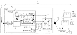
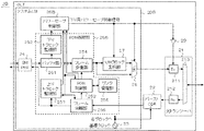
本発明を実施する実施の形態1におけるPONシステムを図1ないし図8を用いて説明する。図1において、PONシステム1は上位装置4と加入者端末であるTE(Terminal Equipment)5の間に設けられ、上位装置4のネットワーク側に接続された通信装置であるOLT(Optical Line Terminal)2すなわち親局装置と、TE5a~5nに接続したONU(Optical Network Unit)3a~3nすなわち子局装置と、OLT2およびONU3a〜3nを接続する光ファイバ6と、光ファイバ6の途中に配置され、OLT2から送信された光信号を各ONU3a〜3n向けに分岐する光カプラ7とで構成されている。TE5としては、例えばHGW(Home Gate Way)、VoIP(Voice over Internet Protocol−Terminal Adapter)、PCなどがある。
ここではONU3がn台(nは整数)接続された場合を示しているが、1台以上であれば何台でも良く、各ONU3に接続するTE5も1台のみならず複数台であっても良い。また、PONシステム1では一般に、OLT2からONU3向きを下り方向、ONU3からOLT2向きを上り方向と呼ぶ。
The PON system in
In this example, n ONUs 3 (n is an integer) are connected. However, any number of ONUs 3 may be used as long as it is 1 or more, and not only one TE5 but also a plurality of TE5s may be connected. good. In the
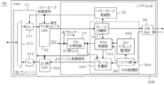
OLT2は、CMOS半導体等で形成された電気信号を処理するシステムLSI20と、システムLSI20で処理する電気信号と光ファイバ6上を伝送する光信号とをE/O変換またはO/E変換する光トランシーバ21と、光トランシーバ21を駆動する駆動回路29とを備えている。また、光トランシーバ21とシステムLSI20の間にはバーストCDR(Clock and Data Recovery)22が設けられ、ONU3からバースト的に送信される信号を入力としてデータとクロックを再生すると共に、システムLSI20上の各素子を駆動する基準クロック23へ載せ替えを行っている。
The
システムLSI20は、基準クロック23と、上位装置4と信号の送受信を行うSNI(Service Node Interface)PHY24と、GE−PON(ギガビットEthernet(登録商標)−PON)システムのPON処理と同等のフレーム処理機能を有するPON処理部25すなわち送信データ処理部、下りトラヒック量に基づいて通常運用状態とパワーセーブ状態とを切り替えるパワーセーブ制御信号すなわち親局制御信号を生成すると共に、パワーセーブする時間情報を有効データとして生成し、PON処理部25に転送するパワーセーブ制御部26と、基準クロック23をN分周(Nは整数)して低速クロックを生成する1/Nクロック生成部27すなわち低速クロック生成部と、パワーセーブ制御信号に基づいてPON処理部25から出力されるフレームを1/Nクロックに切替えるセレクタ28と、を備えている。
The
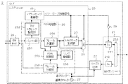
PON処理部25は、図2に示すように、SNI−PHY24からのデータを一時的に蓄積するバッファ部251と、上位装置4からPONシステム1へ送信する下りデータのトラヒック量を監視する下りトラヒック監視部252と、制御フレームを生成してONU3との間で送受信することによりPONシステム1区間を制御するPON制御部253と、バッファ部251およびPON制御部253から出力された有効データをフレームとして多重するフレーム多重部254と、PON制御部253と連動してONU3との間のリンク状態を管理するリンク管理部255と、ONU3から受信したフレームをユーザデータフレームと制御フレームに分離するフレーム分離部256を備えている。
なお、データ処理を行う各ブロックはソフトウェアで構成しても良い。
As shown in FIG. 2, the PON processing unit 25 includes a buffer unit 251 that temporarily accumulates data from the SNI-
Each block for data processing may be configured by software.
光トランシーバ21は駆動回路29の出力に基づいて、システムLSI20から入力された電気信号を出力P1の高速光信号または出力P2の低速光信号にE/O変換してPONシステム1に送信する光送信器211と、PONシステム1から受信した光信号を電気信号にO/E変換してシステムLSI20へ出力する光受信器212と、送信光信号及び受信光信号を合分波する光合分波器213とで構成されている。
なお、低速光信号の出力P2は高速光信号の出力P1よりも小さく、例えば高速光信号の伝送速度が10GHz程度であれば駆動電流20mA程度の出力強度を要するのに対し、伝送速度が100MHz程度まで低速化すると駆動電流3mA程度の出力強度に抑えることができる。
Based on the output of the drive circuit 29, the
The output P2 of the low-speed optical signal is smaller than the output P1 of the high-speed optical signal. For example, if the transmission speed of the high-speed optical signal is about 10 GHz, an output intensity of about 20 mA is required, whereas the transmission speed is about 100 MHz. If the speed is reduced to about 3, the output intensity can be suppressed to about 3 mA.
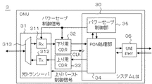
ONU3は、図3に示すように、光ファイバ6上を伝送する光信号を電気信号にO/E変換すると共に、ONU3内で用いた電気信号を光ファイバ6上を伝送する光信号にE/O変換する光トランシーバ31すなわち受信部と、CMOS半導体等で形成され、電気信号を処理するシステムLSI30と、光トランシーバ31とシステムLSI30との間に設けられ、PONシステム1から受信した信号に基づいてデータおよびクロックを再生する下り用CDR32すなわちクロック再生部と、システムLSI30から受取った信号を整形すると共にタイミング調整を行う上り用CDR33とを備えている。
As shown in FIG. 3, the ONU 3 O / E converts an optical signal transmitted on the optical fiber 6 into an electrical signal, and converts the electrical signal used in the
システムLSI30は、制御フレームを生成してOLT2との間で送受信することによりPONシステム1区間の制御、すなわちPON制御を行うPON処理部34と、PON処理部34と連携してOLT2がパワーセーブする時間情報を抽出し、パワーセーブ制御信号すなわち子局制御信号を生成するパワーセーブ制御部35と、TE5と信号の送受信を行うUNI(User Network Interface)PHY36とを備え、下り用CDR32で抽出された再生クロックに同期して動作する。
The
光トランシーバ31は、パワーセーブ制御信号に基づいてPONシステム1から受信した高速光信号および低速光信号を同程度の光強度に増幅し、O/E変換して下り用CDR32へ出力する光受信器311と、上り用CDR33から入力された電気信号を所定強度の光信号にE/O変換してPONシステム1に送信する光送信器312と、送信光信号及び受信光信号を合分波する光合分波器313とで構成されている。
The
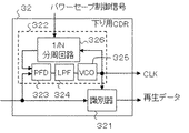
下り用CDR32は、図4に示すように、光受信器311からの入力信号とフィードバック信号の位相差を検出する位相比較器323と、位相比較器323の出力を平均化し、電圧として出力するループフィルタ324と、ループフィルタ324の電圧を所定の発振周波数で発振するようフィードバック制御するVCO(Voltage Controlled Oscillator)325すなわち電圧制御発振器と、で構成されたPLL(Phase−locked Loop)回路322と、再生したクロックに同期して受信したデータを再生する識別器321を備えている。また、VCO325から位相比較器323へのフィードバック回路の途中にはパワーセーブ制御信号に基づいて分周率が変化する1/N分周回路326すなわち可変分周器が設けられている。
As shown in FIG. 4, the
なお、PONシステム1はGE−PONシステムと同様に、リンクを維持するため定期的にOLT2のPON制御部253とONU3のPON処理部34の間で制御フレームをやり取りして、リンクが維持されている場合にのみデータ通信を行う。
As in the GE-PON system, the
次に動作について説明する。
まず、下り方向の通信について説明する。OLT2は、上位装置4からSNI−PHY24を介して入力されたデータはバッファ部251及び下りトラヒック監視部252に送られ、バッファ部251に一次蓄積されたデータはその後フレーム多重部254に送られる。下りトラヒック監視部252は下り方向のトラヒック量を監視し、その情報をパワーセーブ制御部26に伝達する。パワーセーブ制御部26は下りトラヒック監視部252から受取ったトラヒック情報、PON制御部253がPON制御を行う制御フレームのトラヒック情報、およびパワーセーブ制御部26自身が生成するパワーセーブの時間情報を格納したパワーセーブ制御フレームのトラヒック情報を合わせて有効データとし、この有効データの有無を判定して有効データが無い場合にパワーセーブ制御信号をLow出力する。
Next, the operation will be described.
First, downlink communication will be described. In the
PON制御部253はパワーセーブ制御信号に基づいて、ONU3とのリンク維持やPON制御するための制御フレームを生成すると共に、パワーセーブ制御部26から受取ったパワーセーブ制御フレームをフレーム多重部254へ出力する。フレーム多重部254はバッファ部251からのデータフレームとPON制御部253からのフレームを時分割多重して出力する。
なお、ここではリンク維持やPON制御の詳細説明は省略するが、例えばGE−PONシステムと同様にプロトコルの一種であるMPCP(Multi−Point Control Protocol)を利用すれば、DiscoveryプロセスやGate/Reportプロセスで実現できる。
The PON control unit 253 generates a control frame for maintaining the link with the
Although detailed description of link maintenance and PON control is omitted here, for example, if the MPCP (Multi-Point Control Protocol), which is a type of protocol, is used as in the GE-PON system, the Discovery process and the Gate / Report process Can be realized.
フレーム多重部254の出力は2つに分岐された後、一方は1/Nクロック生成部27に入力され、他方は直接セレクタ28に送られる。1/Nクロック生成部27は入力信号を元に基準クロック23をN倍に低速化した低速クロックデータを生成し、パワーセーブ制御信号がLow、すなわち有効データが無くIDLEデータで補間された状態を示しているとき、フレーム多重部254からの信号を低速クロックデータに置換したデータをセレクタ28へ出力する。セレクタ28はパワーセーブ制御信号に基づいて、有効データが有る状態ではフレーム多重部254から入力される有効データを、有効データが無い状態では1/Nクロックデータを選択して光送信器211へ出力する。
なお、1/Nクロック生成部27では常時低速クロックを出力し、セレクタ28にてパワーセーブ制御信号に対応した有効データと低速クロックデータの出力切り替えを行っても良い。
After the output of the
Note that the 1 /
パワーセーブ制御信号は光トランシーバ21の駆動回路29にも伝えられ、駆動回路29はこれを元に光送信器211の光出力強度を切替える制御信号を生成する。光送信器211はシステムLSI20から電気信号が入力されると光信号にE/O変換し、この光信号を駆動回路29からの制御信号に応じて出力強度P1またはP2に調整してPONシステム1に向けて送信する。
The power save control signal is also transmitted to the drive circuit 29 of the
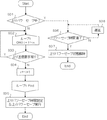
ここで、図5は上記OLT2のシステムLSI20について、下り通信用の各機能をソフトウェアで構成した場合の動作を説明するフローチャートである。
システムLSI20はパワーセーブ中であるか否かを判定し(S1)、パワーセーブ中で無い、すなわち通常運用状態であると判定すれば上位装置4から下りデータのトラヒックが有るか無いかを確認する(S2)。下りトラヒックが無い場合はパワーセーブ状態の開始時間及び継続時間を決定し(S3)、これらの時間情報を格納したパワーセーブ制御フレームを生成し(S4)、ONU3へ送信する(S8)。その後、パワーセーブ制御信号の出力タイミングに合わせてOLT2全体をパワーセーブ状態に遷移させ、PONシステム1に向けて低速の1/Nクロックデータを低出力で送信する(S5)。パワーセーブ状態にあるOLT2は定期的にパワーセーブ制御の継続時間が満了したか否かを確認し(S6)、継続時間満了であると判定するとS7にてパワーセーブ状態を解除し、S1の工程に戻る。なお、パワーセーブ状態の解除とは、通常運用状態で高速かつ高出力の光信号を送信することを意味する。
Here, FIG. 5 is a flowchart for explaining the operation of the
The
S1においてパワーセーブ中であると判定した場合、パワーセーブ状態にあるOLT2はS6にてパワーセーブ制御の継続時間が満了したか否かを確認する。また、S2において下りトラヒックが有ると判断した場合、高速かつ高出力の光信号としてONU3へデータを送信する(S8)。S8では下りトラヒックの他に、PON制御に必要な制御フレームや上記のパワーセーブ制御フレームも有効データとして高速かつ高出力の光信号に変換して送信する。S6においてパワーセーブ制御の継続時間が満了していない場合は、予め定めた期間だけ待って(S9)再びS6の工程に戻る。
なお、図内の実線は通常運用状態を、破線はパワーセーブ状態であることを示している。
If it is determined in S1 that power saving is in progress, the
The solid line in the figure indicates the normal operation state, and the broken line indicates the power save state.
このように、OLT2は有効データの有無に応じて、有効データ送信用の高速かつ高出力の光信号と、この光信号にタイミング同期した低速クロックデータ送信用の低速かつ低出力の光信号とを切替えることにより、消費電力を低減できる。
なお、ここでいう高速/低速および高出力/低出力とは2種類の光信号を比較した場合の速度および出力強度であり、具体的な基準によるものでは無い。
As described above, the
The high speed / low speed and the high output / low output here are the speed and output intensity when two types of optical signals are compared, and are not based on specific standards.
一方、ONU3は、PONシステム1から光信号が入力されると、光トランシーバ31の光受信器311で受信する。光受信器311は光信号をパワーセーブ制御信号に基づいて所定レベルに増幅した後に電気信号にO/E変換し、下り用CDR32に出力する。
On the other hand, when an optical signal is input from the
下り用CDR32は電気信号を2分岐して一方を識別器321に、他方をPLL回路322の位相比較器323に送る。位相比較器323は光受信器311からの信号とVCO325からのフィードバック信号を入力としてループフィルタ324に位相差を出力し、ループフィルタ324は入力された2つの信号の位相差を平均化して電圧に変換した値をVCO325に出力する。VCO325は所定の発振周波数で発振するため、PLL回路322はフィードバック制御を行って適切な電圧が得られるように調整する。
The
フィードバック回路の途中に設けられた1/N分周回路326はパワーセーブ制御信号に基づいて適切な分周率に切り替えられ、VCO325からの信号をN分周して位相比較器323に出力する。PLL回路322の出力は再生クロックとして識別器331に送られ、入力データのたたき直しに用いられる。識別器321にてたたき直されたデータは再生データとして、再生クロックと共にシステムLSI30に送られる。
The 1 / N
システムLSI30に送られたデータは、PON処理部34にて上位装置4からのデータを格納したデータフレーム、PON制御に用いられる制御フレーム、パワーセーブ用のパワーセーブ制御フレームに分離され、データフレームはUNI−PHY36を介してTE5に転送される。一方、制御フレームはGE−PONシステムと同様にPON処理部34内でPON制御に用いられ、パワーセーブ制御フレームはパワーセーブ制御部35に転送される。
The data sent to the
パワーセーブ制御部35はOLT2がパワーセーブする時間情報をパワーセーブ制御フレームから抽出し、自装置であるONU3用のパワーセーブ制御信号を生成する。例えば光受信器311に高速光信号の受信状態を示すHighレベルのパワーセーブ制御信号が入力されると、光受信器311は受信信号の増幅前の光強度は駆動電流20mA程度であるとし、低速光信号の受信状態を示すLowレベルのパワーセーブ制御信号が入力されると、増幅前の光強度が駆動電流3mA程度であるとして、受信した光信号を同レベルの強度まで増幅した後に電気信号にO/E変換する。
The power save
ここで、高速光信号の周波数が10GHz、低速光信号の周波数が1GHzの場合を例として1/N分周回路336の切替え動作について説明する。
下り用CDR32に高速光信号の受信状態を示すパワーセーブ制御信号が入力されると、1/N分周回路336の分周率はN=1に設定され、低速光信号の受信状態を示すパワーセーブ制御信号が入力されると、1/N分周回路336の分周率はN=10に変更される。
Here, the switching operation of the 1 / N
When the power saving control signal indicating the reception state of the high-speed optical signal is input to the
このように、パワーセーブ制御信号に基づいて分周率可変の1/N分周回路336を用いることにより、ONU3はOLT2から速度及び強度の異なる光信号を受信しても常に高速データの処理速度と等しいクロックを抽出できる。
また、ONU3はパワーセーブ制御信号に応じて、自身のPON処理部34の下り方向の機能をスリープさせて省電力化を図ることもできる。
As described above, by using the 1 / N
The
ここで、図6は上記ONU3のシステムLSI30について、各機能をソフトウェアで構成した場合の動作を説明するフローチャートである。
システムLSI30はパワーセーブ中であるか否かを判定し(S11)、パワーセーブ中で無いと判定すればパワーセーブ制御フレームを受信しているか否かを確認する(S12)。パワーセーブ制御フレームを受信している場合はパワーセーブ状態の開始時間及び継続時間の情報を抽出し(S13)、これらの時間情報に合わせて自装置向けのパワーセーブ制御信号を出力すると共に、ONU3全体をパワーセーブ状態に遷移させる(S14)。S12にてパワーセーブ制御フレームを受信していないと判断した場合は予め定めた期間だけ待って(S17)、再度S12の工程を繰り返す。
Here, FIG. 6 is a flowchart for explaining the operation when the functions of the
The
S11にてパワーセーブ中であると判定した場合、パワーセーブ状態にあるONU3は定期的にパワーセーブ制御の継続時間が満了したか否かを確認し(S15)、継続時間満了であると判定するとパワーセーブ状態を解除し(S16)、高速かつ高出力の光信号を受信できる状態(S11)に戻る。また、S15においてパワーセーブ制御の継続時間が満了していないと判定した場合も予め定めた期間だけ待って(S18)、再びS15の工程に戻る。
なお、図内の実線は通常運用状態を、破線はパワーセーブ状態であることを示している。
If it is determined in S11 that power saving is in progress, the
The solid line in the figure indicates the normal operation state, and the broken line indicates the power save state.
ところで、図7はOLT2及びONU3のパワーセーブ制御信号とこれに関連する信号の出力タイミングを示す図である。ただし、この図は動作を模式的に示すものであって内部回路遅延等によるタイミング誤差は含んでおらず、また、GE−PONシステムと同様にOLT2とONU3は時刻同期していることを前提としている。ここでいう時刻同期とは、すなわち、OLT2が自身の内部クロックで時刻T0のときにONU3へフレームを送信すると、ONU3はこのフレームを受信する時刻が自身の内部クロックの時刻T0となるよう調整することを意味する。
FIG. 7 is a diagram showing the output timing of the
図7(a)はOLT2及びONU3がそれぞれ自装置に対してパワーセーブ制御信号を出すタイミングを示しており、OLT2のセレクタ28は、パワーセーブ制御信号の出力がHighで通常運用状態を示しているときは図7(b)に示すように有効データを出力し、パワーセーブ制御信号の出力がLowでパワーセーブ状態を示しているときは図7(c)に示すように1/Nクロックデータを出力する。
FIG. 7A shows the timing at which the
OLT2の光送信器211は、図7(d)に示すように、有効データの出力時は高速伝送に耐えられるよう比較的強度の大きな出力P1で光信号を送信し、1/Nクロックデータの出力時は出力P1よりも強度の小さな出力P2で光信号を送信する。これに対し、ONU3の光受信器311は、図7(e)に示すように、有効データの高速光信号および1/Nクロックデータの低速光信号が同じ光強度となるよう増幅し、E/O変換して電気信号として出力する。また、上述のとおり、ONU3の下り用CDR32はパワーセーブ制御信号に応じて1/N分周回路336の分周率を適切な値に切替えるため、図7(f)に示すように、パワーセーブ状態であるか否かに関わらず常に有効データの処理速度と等しいクロックを抽出できる。
As shown in FIG. 7D, the
このように、OLT2がパワーセーブする時間に対応してONU3のパワーセーブ制御信号を生成することにより、OLT2が速度及び強度の異なる光信号を送信してもONU3は常に有効データの処理速度と等しいクロックを再生できるため、有効データを損なうこと無く受信できる。
Thus, by generating the power saving control signal of the
次に、上り方向の通信について説明する。
ONU3は、TE5からユーザデータフレームを受信すると、UNI−PHY37を介してPON処理部34に取り込み、PON制御用の制御フレームと時間多重して上り用CDR33に出力する。
なお、10GHz程度の高速信号を伝送する場合、ONU3は送信信号の波形整形及びタイミング調整をするために上り用CDR33を用いる必要がある。上り方向のデータは各ONU3からバースト的に出力されるが、上り用CDR33の同期確立には数秒程度を要するため、有効データの不在時にはPON処理部34にてIDLEデータを補間し、システムLSI30と上り用CDR33の間は有効データの有無に関わらず連続的にデータ伝送する。
Next, uplink communication will be described.
When the
When transmitting a high-speed signal of about 10 GHz, the
上り用CDR33はPON処理部34から入力された信号を、タイミング調整すると共に波形整形して光トランシーバ31の光送信器312に送る。PON処理部34はまた、ユーザデータフレーム及び制御フレームで構成される有効データのバースト送出期間と、バースト補間期間とを信号レベルHigh/Lowで識別する上りバースト制御信号を生成し、光トランシーバ31に出力する。光送信器312は受け取った電気信号を予め定めた出力強度の光信号にE/O変換し、上りバースト制御信号がHighレベルで有効データ送出期間を示しているとき、PONシステム1に向けてこの光信号を送信する。上りバースト制御信号がLowレベルで上りバーストデータが不在の時は、光トランシーバ31からは何も送信しない。
The
一方、OLT2はPONシステム1を伝送してきた光信号を、光合分波器213を介して光受信器212にて受信し、所定レベルの信号に増幅した後に電気信号にO/E変換してバーストCDR22に出力する。バーストCDR22は入力信号からデータとクロックを再生すると共に、再生したデータを基準クロック23にクロック載せ替えし、システムLSI20に出力する。
On the other hand, the
システムLSI20に入力された再生データは、フレーム分離部256にてユーザデータフレームと制御フレームとに分離される。分離されたユーザデータフレームはSNI−PHY24を介して上位装置4に転送され、制御フレームはPON制御部253に送られる。PON制御部253は、GE−PONシステムと同様に、制御フレームを用いてPON制御を行うと共にリンク管理部255と連携してONU3とのリンク維持を図る。
The reproduction data input to the
ここまでは各装置の動作である。続けてPONシステム1のシステム動作について説明する。
図8は下り方向のパワーセーブ制御シーケンスを示す図である。例えば(1)のように上位装置4からのデータが有る場合、OLT2の下りトラヒック監視部252はパワーセーブ制御部26にその情報を伝え、パワーセーブ制御部26はPON処理部25にデータを出力させる。ONU3はこのデータを受信すると、PON処理部34にて有効データとして処理する。
The operation so far is the operation of each device. Next, the system operation of the
FIG. 8 is a diagram showing a power saving control sequence in the downlink direction. For example, when there is data from the
ところで(2)のように上位装置4からOLT2へのデータが無い場合、下りトラヒック監視部252は下りトラヒックが無いという情報をパワーセーブ制御部26に伝える。パワーセーブ制御部26はPON処理部35が生成する制御フレーム等のトラヒック情報も加味して予め定めた継続時間Tsだけパワーセーブすることを決め、パワーセーブ制御の開始時間および継続時間の情報を格納したパワーセーブ制御フレームを生成してONU3へ送信する。その後、パワーセーブ制御部26は決定した開始時間から所定の継続時間が満了するまでの間、自装置内をパワーセーブ状態にするパワーセーブ制御信号を出力し、光トランシーバ21はこのパワーセーブ制御信号に対応して1/N低速クロックデータをONU3に連続的に送信する。
By the way, when there is no data from the
ONU3はパワーセーブ制御フレームを受信すると、パワーセーブ制御部35にてフレーム内に格納されたパワーセーブ制御の開始時間および継続時間Tsの情報を抽出し、OLT2のパワーセーブ状態に対応できるよう自装置向けのパワーセーブ制御信号を生成する。このパワーセーブ制御信号はOLT2がパワーセーブ状態を解除してデータ送信してきた場合に、データを損なうこと無く受信できるタイミングでONU3の各構成要素に対して出力される。図8ではパワーセーブ制御部35からPON処理部34にパワーセーブ状態解除を指示するActivate Requestを出力しているが、同時にパワーセーブ制御信号を用いて光受信器311及び下り用CDR32にもパワーセーブ状態の解除を指示することは言うまでもない。
When the
さて、(3)のようにパワーセーブ中に上位装置4からデータが送られてきた場合、下りトラヒック監視部252はその情報をパワーセーブ制御部26に伝える。OLT2のパワーセーブ状態は継続時間Ts満了まで継続され、このデータはバッファ部251に一時蓄積される。パワーセーブ制御部26は継続時間Tsが満了すると、下りトラヒック監視部252よりデータ有りの情報を受けたか否かを確認し、データがある場合にはバッファ部251に一次蓄積したデータをONU3へ送信させる。
When data is sent from the
バッファ部251に蓄積されたデータをすべて送出すると、OLT2は再び下りトラヒック監視部252より(4)のようなデータ無しの情報を受取る、あるいは予め定めた所定時間に何も情報を受取らなければ、上記(2)と同様にパワーセーブ状態に遷移する。(5)のように、パワーセーブ継続時間Tsの満了時までに下りトラヒック監視部252からデータ有りの情報が伝達されていなければ、パワーセーブ制御部26は下りトラヒックが無いと判断してOLT2のパワーセーブ状態を継続するようパワーセーブ制御フレームをONU3宛に送信する。(5)のデータは上記(3)と同様に、次のパワーセーブ継続時間Tsが満了するまでバッファ部251にて一次蓄積され、その後ONU3へ送信される。以降、OLT2及びONU3は同様の動作を繰り返す。
When all the data stored in the buffer unit 251 is transmitted, the
この実施の形態によれば、OLT2は有効データのトラヒック有無に応じてパワーセーブ制御信号を生成し、通常運用状態では高速かつ出力強度の大きな光信号を送信すると共に、パワーセーブ状態では低速かつ通常運用状態よりも出力強度の小さな光信号を送信することにより、消費電力を低減できる。
According to this embodiment, the
また、OLT2はパワーセーブ状態の開始時間及び継続時間の情報を格納したパワーセーブ制御フレームを生成してONU3へ送信し、ONU3はこのパワーセーブ制御フレームを受信すると上記の時間情報を抽出して自装置向けのパワーセーブ制御信号を生成してパワーセーブ制御を行うことにより、ONU3はOLT2が速度及び強度の異なる光信号を送信しても常に有効データの処理速度と等しいクロックを抽出することができ、有効データを損なうこと無く受信できる。さらに、ONU3はパワーセーブ制御信号に応じて自身のPON処理部34における下り方向の機能をスリープさせて省電力化を図ることもできる。
また、このようなOLT2及びONU3で構成されるPONシステム1も、有効データを損失すること無く消費電力を低減できる。
The
Further, the
実施の形態2.
上記実施の形態1ではOLTのパワーセーブについて示したが、実施の形態2ではあわせてONUのパワーセーブも行う。本実施の形態に係るPONシステムを図9ないし図12を用いて説明する。なお、実施の形態1と同じ構成については同一符号を付して説明を省略する。
Although the OLT power save is shown in the first embodiment, the ONU power save is also performed in the second embodiment. A PON system according to the present embodiment will be described with reference to FIGS. Note that the same components as those in the first embodiment are denoted by the same reference numerals and description thereof is omitted.
PONシステム1及びOLT2の構成は実施の形態1と同じである。また、ONU3Aも図9に示すように、システムLSI30Aと下り用CDR32A以外は実施の形態1と同じ構成を有し、CMOS半導体等で形成されるシステムLSI30Aは、PON処理機能を有するPON処理部34Aと、パワーセーブ制御部35すなわち第1の子局制御部と、UNI−PHY37とを備えている。
The configurations of the
PON処理部34Aは、下り方向のフレームをPON制御用の制御フレーム、パワーセーブ制御フレーム、データフレームに分離するフレーム分離部341と、TE5から受信した上り方向のユーザデータを一時的に蓄積するバッファ部342と、上り方向のユーザデータのトラヒック有無を監視する上りトラヒック監視部343と、OLT2との間でPON制御を行うPON制御部345すなわち第2の子局制御部と、バッファ部342に一次蓄積されたユーザデータのデータフレーム及びPON制御部345からの制御フレームを時分割多重するフレーム多重部344とで構成されている。
The
また、下り用CDR32Aすなわちクロック再生部は、図10に示すように、実施の形態1に記載のPLL回路322および識別器321に加え、PON制御部345からの上りバースト制御信号すなわち第2の子局制御信号に基づいて再生クロックを分周率M(Mは整数)で低速化する1/M分周回路327すなわち可変分周器を備えている。
システムLSI30A上の各ブロックは下り用CDR32Aで抽出した再生クロックに同期して動作するが、フレーム多重部344は1/M分周回路327から出力される上り用クロックに同期して動く。
Further, as shown in FIG. 10, the
Each block on the system LSI 30A operates in synchronization with the reproduction clock extracted by the
上り用CDR33Aは、図11に示すように、フレーム多重部344からの入力信号とフィードバック信号の位相差を検出する位相比較器333と、位相比較器333の出力を平均化し、電圧として出力するループフィルタ334と、ループフィルタ334の電圧を所定の発振周波数で発振するようフィードバック制御するVCO335とで構成されたPLL回路332と、再生したクロックに同期して受信したデータを再生する識別器331を備えている。また、VCO335から位相比較器333へのフィードバック回路の途中には上りバースト制御信号に基づいて分周率が変化する1/N分周回路336が設けられている。
As shown in FIG. 11, the
次に動作について説明する。
まず、下り方向の通信について説明する。OLT2は実施の形態1と同じため、説明を省略する。
一方、ONU3AはPONシステム1から光信号が入力されると、光トランシーバ31の光受信器311で受信する。光受信器311は光信号をパワーセーブ制御信号に基づいて所定レベルに増幅した後に電気信号にO/E変換し、下り用CDR32Aに出力する。
Next, the operation will be described.
First, downlink communication will be described. Since the
On the other hand, when the optical signal is input from the
下り用CDR32Aでは電気信号を2分岐して一方を識別器321、他方をPLL回路322の位相比較器323に送る。位相比較器323は光受信器311からの信号とVCO325からのフィードバック信号を入力としてループフィルタ324に位相差を出力し、ループフィルタ324は入力された2つの信号の位相差を平均化して電圧に変換した値をVCO325に出力する。VCO325は所定の発振周波数で発振するため、PLL回路322はフィードバック制御を行って適切な電圧が得られるように調整する。
In the
フィードバック回路の途中に設けられた1/N分周回路326は下り用パワーセーブ制御信号に基づいて適切な分周率に切り替えられ、VCO325からの信号をN分周して位相比較器323に出力する。PLL回路322の出力は再生クロックとして識別器321に送られ、入力データのたたき直しに用いられる。識別器321にてたたき直されたデータは再生データとして、再生クロックと共にシステムLSI30Aに送られる。
The 1 / N
また、1/M分周回路327はPON制御部345からの上りバースト制御信号の立下りエッジを検出すると再生クロックを分周率Mで低速化し、上りバースト制御信号の立上りエッジを検出すると再生クロックそのものを上り用クロックとしてシステムLSI30Aのフレーム多重部344に出力する。
Further, the 1 / M
システムLSI30Aに送られた再生データは、フレーム分離部341にて上位装置4からのデータを格納したデータフレーム、PON制御に用いられる制御フレーム、下りパワーセーブ用のパワーセーブ制御フレームに分離され、データフレームはUNI−PHY37を介してTE5に転送される。一方、制御フレームはGE−PONシステムと同様にPON制御部345に送られ、パワーセーブ制御フレームはパワーセーブ制御部35に転送される。
The reproduction data sent to the system LSI 30A is separated into a data frame in which data from the
パワーセーブ制御部35はOLT2が下り方向のパワーセーブを実行する時間情報を受信したパワーセーブ制御フレームから抽出し、自装置であるONU3A用のパワーセーブ制御信号を生成する。例えば光受信器311に高速光信号の受信状態を示すHighレベルのパワーセーブ制御信号が入力されると、光受信器311は受信信号の増幅前の光強度は駆動電流20mA程度であるとし、低速光信号の受信状態を示すLowレベルのパワーセーブ制御信号が入力されると、増幅前の光強度が駆動電流3mA程度であるとして、受信した光信号を同レベルの強度まで増幅した後に電気信号にO/E変換する。
The power save
ここで、高速光信号の周波数が10GHz、低速光信号の周波数が1GHzの場合を例として1/N分周回路336の切替え動作について説明する。
下り用CDR32Aに高速光信号の受信状態を示すパワーセーブ制御信号が入力されると、1/N分周回路336の分周率はN=1に設定され、低速光信号の受信状態を示すパワーセーブ制御信号が入力されると、1/N分周回路336の分周率はN=10に変更される。
Here, the switching operation of the 1 / N
When the power saving control signal indicating the reception state of the high-speed optical signal is input to the
このように、パワーセーブ制御信号に基づいて分周率可変の1/N分周回路336を用いることにより、ONU3AはOLT2から速度及び強度の異なる光信号を受信しても常に高速データの処理速度と等しいクロックを抽出できる。
また、ONU3AはOLT2が下り方向のパワーセーブを実行する時間に対応して下り用パワーセーブ制御信号を生成することにより、OLT2が速度及び強度の異なる光信号を送信しても常に有効データの処理速度と等しいクロックを再生でき、有効データを損なうこと無く受信できる。
また、ONU3Aはパワーセーブ制御信号に応じて、自身のPON処理部34Aの下り方向の機能をスリープさせて省電力化を図ることもできる。
また、実施の形態1と同様に、システムLSI30Aの下り方向通信に関する各機能をソフトウェアで構成することもできる。
As described above, by using the 1 / N
Further, the ONU 3A generates a downstream power save control signal corresponding to the time when the
The ONU 3A can also save power by sleeping the downstream function of its own
Similarly to the first embodiment, each function related to the downlink communication of the system LSI 30A can be configured by software.
次に、上り方向の通信について説明する。
ONU3Aは、TE5からユーザデータフレームを受信すると、UNI−PHY37を介してPON処理部34A内のバッファ部342に取り込む。バッファ部342はユーザデータを一時的に蓄積すると共に上りトラヒック監視部343に転送し、上りトラヒック監視部343は上りトラヒック量の情報をパワーセーブ制御部35に伝達する。
Next, uplink communication will be described.
When receiving the user data frame from the TE 5, the ONU 3A takes in the buffer unit 342 in the
PON制御部345はOLT2とのリンク維持やPON制御するための制御フレームを生成するのに加え、この制御フレームのトラヒック情報と上りトラヒック監視部343から受取ったユーザデータのトラヒック情報から上り有効データの有無を判定する。上り有効データが有ると判定した場合は、OLT2から受信した制御フレームの情報に基づいてフレーム多重部344にデータ送信指示をすると共に、下り用CDR32Aと光トランシーバ31へ上りバースト送信タイミングにあわせて上りバースト制御信号をHighレベルで出力する。一方、上りバーストデータが無いと判定した場合はフレーム多重部344へは何も指示せず、下り用CDR32Aと光トランシーバ31へ上りバースト制御信号をLowレベルで出力する。
The
バッファ部342で一時蓄積されたユーザデータフレーム及びPON制御部345で生成された制御フレームは共にフレーム多重部344に伝達され、PON制御部345の指示に基づいて、時分割多重で上り用CDR33Aに送られる。なお、フレーム多重部344はユーザデータフレーム及び制御フレームの不在時にはIDLEデータを補間して連続信号を出力する。
Both the user data frame temporarily stored in the buffer unit 342 and the control frame generated by the
ところで、フレーム多重部344と上り用CDR33A間の高速信号伝送には非常に大きな電力消費を伴う。PON制御部345は有効データを送出時には上りバースト制御信号をHighレベルで出力するため、下り用CDR32Aは上りバースト制御信号の立上りエッジを検出して再生クロックを上り用クロックとして出力し、フレーム多重部344はこの再生クロックに同期して動作する。
By the way, high-speed signal transmission between the
一方、上りバーストデータ不在時にはPON制御部345は上りバースト制御信号をLowレベルで出力するため、下り用CDR32Aは上りバースト制御信号の立下りエッジを検出して再生クロックを分周率Mで低速化したクロックを上り用クロックとして出力し、フレーム多重部344は低速クロックに同期して動作する。
このようにして、上りバーストデータ不在時にフレーム多重部344と上り用CDR33A間を低速クロックで動作に切替えることにより、消費電力が大幅に低減できる。
On the other hand, when the upstream burst data is absent, the
In this way, the power consumption can be greatly reduced by switching the operation between the
ところで、上り用CDR33Aに設けられた1/N分周回路336の分周率は上りパワーセーブ制御信号に基づいて適切な値に切り替えられる。例えば、周波数が10GHzの高速光信号が入力される場合、上りバースト制御信号も入力されて分周率はN=1となり、周波数が1GHzの低速光信号で上りバースト制御信号が入力されない場合、分周率はN=10に切り替えられる。このように、上り用CDR33AのVCO335は入力データの速度によらず安定的に発振するため、上り用CDR33Aに入力されたデータはタイミング調整及び波形整形され、光トランシーバ31の光送信器312に送られる。
Incidentally, the frequency division ratio of the 1 / N
光送信器312は受け取った電気信号を予め定めた出力強度の光信号にE/O変換し、PON制御部345からの上りバースト制御信号がHighレベルで上りバーストデータの送出期間を示しているときはPONシステム1に向けてこの光信号を送信し、上りバースト制御信号がLowレベルのときは上りバーストデータが不在なので光トランシーバ31からは何も送信しない。
The
ここで、図12は上記ONU3AのシステムLSI30Aについて、上り方向のパワーセーブに関する各機能をソフトウェアで構成した場合の動作を説明するフローチャートである。
まず、上り方向のパワーセーブ中であるか否かを判定し(S21)、パワーセーブ中で無い、すなわち通常運用状態であると判定すればTE5から上りデータのトラヒック送信要求が有るか無いかを確認する(S22)。上り送信要求が無い場合は下り用CDR32A及び光トランシーバ31へ上りバースト制御信号をLow出力し(S23)、上り方向のパワーセーブを実行するために下り用CDR32Aに上り用低速クロックを生成させ、システムLSI30Aと上り用CDR33A間を低速で信号伝送させ(S24)、フローを終了する。
Here, FIG. 12 is a flowchart for explaining the operation of the ONU 3A system LSI 30A when the functions related to the upstream power saving are configured by software.
First, it is determined whether or not uplink power saving is in progress (S21). If it is determined that power saving is not being performed, that is, the normal operation state, it is determined whether or not there is an uplink data traffic transmission request from TE5. Confirm (S22). When there is no upstream transmission request, the upstream burst control signal is output low to the
S21においてパワーセーブ中であると判定した場合も、TE5から上りデータのトラヒック送信要求が有るか無いかを確認し(S25)、上り送信要求が有る場合は下り用CDR32A及び光トランシーバ31へ上りバースト制御信号をHigh出力し(S26)、上り方向のパワーセーブ状態を解除してシステムLSI30Aと上り用CDR33A間を下り用CDR32Aが抽出する再生クロックに同期して高速で信号伝送させ(S27)、フローを終了する。
Even if it is determined in S21 that power saving is in progress, it is checked whether there is an uplink data traffic transmission request from TE5 (S25). If there is an uplink transmission request, an uplink burst is transmitted to downlink
また、S22において上りトラヒック送信要求が有ると判定した場合はS26に状態遷移し、S25において上りトラヒック送信要求が無いと判定した場合はS23へ状態遷移する。
なお、図内の実線は通常運用状態を、破線はパワーセーブ状態であることを示している。
If it is determined in S22 that there is an upstream traffic transmission request, the state transitions to S26, and if it is determined in S25 that there is no upstream traffic transmission request, the state transitions to S23.
The solid line in the figure indicates the normal operation state, and the broken line indicates the power save state.
ところで、OLT2はPONシステム1を伝送してきた光信号を、光合分波器213を介して光受信器212にて受信し、所定レベルの信号に増幅した後に電気信号にO/E変換してバーストCDR22に出力する。バーストCDR22は入力信号からデータとクロックを再生すると共に、再生したデータを基準クロック23にクロック載せ替えし、システムLSI20に出力する。
By the way, the
システムLSI20に入力された再生データは、フレーム分離部256にてユーザデータフレームと制御フレームとに分離される。分離されたユーザデータフレームはSNI−PHY24を介して上位装置4に転送され、制御フレームはPON制御部253に送られる。PON制御部253は、GE−PONシステムと同様に制御フレームを用いてPON制御を行うと共にリンク管理部255と連携してONU3Aとのリンク維持を図る。
なお、本実施の形態はONU3A内部の動作が実施の形態1と異なるのみで、PONシステム1のシステム動作は同じであるため説明を省略する。
The reproduction data input to the
In this embodiment, only the operation inside the ONU 3A is different from that in the first embodiment, and the system operation of the
この実施の形態によれば、実施の形態1の効果に加えて、ONU3AのPON制御部345がユーザデータフレームと制御フレームで構成される上りバーストデータの送信タイミングにあわせて上りバースト制御信号を生成し、下り用CDR32Aは上りバースト制御信号に基づいて上りバーストデータの不在時に低速クロックを生成し、システムLSI30Aと上り用CDR33A間を低速で信号伝送させることにより、ONU3Aの消費電力を大幅に低減できる。
また、このようなOLT2及びONU3Aで構成されるPONシステムも、有効データを損失すること無く実施の形態1に記載のPONシステム1よりもさらに消費電力を低減できる。
According to this embodiment, in addition to the effects of the first embodiment, the
In addition, the PON system configured by the
実施の形態3.
上記実施の形態2では、上りバーストデータが無い場合にONU3Aの下り用CDR32Aにて低速クロックを生成し、システムLSIと上り用CDR間の消費電力を低減している。本実施の形態では、下り用CDR32Aの代わりにシステムLSI上で上り用の低速クロックを生成する。また、OLTに接続するいずれのONUからも上りバーストデータを受信しない場合に上り方向の機能を休止させてOLTの更なるパワーセーブを図る。本実施の形態に係るPONシステム1を図13ないし図16を用いて説明する。なお、実施の形態1または実施の形態2と同じ構成については同一符号を付して説明を省略する。
In the second embodiment, when there is no upstream burst data, a low-speed clock is generated by the
PONシステム1の構成は実施の形態1と同じである。
OLT2Bは、図13に示すように、システムLSI20B以外は実施の形態1と同じ構成を有し、CMOS半導体等で形成されるシステムLSI20Bは、基準クロック23と、SNI−PHY24と、PON処理機能を有するPON処理部25Bすなわち下りデータ処理部兼上りデータ処理部と、実施の形態1に記載のパワーセーブ制御部26の機能に加えて上り方向のバーストデータ不在時に上りパワーセーブ制御信号すなわち第2の親局制御信号を生成するパワーセーブ制御部26Bと、1/Nクロック生成部27すなわち低速クロック生成部と、下り用パワーセーブ制御信号に基づいてPON処理部25Bから出力されるフレームと1/Nクロックを切替えるセレクタ28を備えている。
The configuration of the
As shown in FIG. 13, the OLT 2B has the same configuration as that of the first embodiment except for the system LSI 20B. The system LSI 20B formed of a CMOS semiconductor or the like has a reference clock 23, an SNI-
PON処理部25Bは、SNI−PHY24からのデータを一時的に蓄積するバッファ部251と、上位装置4からPONシステム1へ送出する下りデータのトラヒック量を監視する下りトラヒック監視部252と、制御フレームを生成してONU3Bとの間で送受信することによりPONシステム1区間を制御するPON制御部253と、バッファ部251およびPON制御部253から出力された有効データをフレームとして多重するフレーム多重部254と、PON制御部253と連動してONU3Bとの間のリンク状態を管理するリンク管理部255と、ONU3Bから受信したフレームをユーザデータフレームと制御フレームに分離するフレーム分離部256に加えて、上りのユーザデータフレームのトラヒック量を監視する上りトラヒック監視部257とで構成されている。
The PON processing unit 25B includes a buffer unit 251 that temporarily accumulates data from the SNI-
一方、ONU3Bは、図14に示すように、システムLSI30B以外は実施の形態1と同じ構成を有し、CMOS半導体等で形成されるシステムLSI30Bは、PON処理機能を有するPON処理部34Aと、パワーセーブ制御部35と、UNI−PHY37に加え、下り用CDR32で抽出された再生クロックをPON制御部345からの上りバースト制御信号に基づいて分周率Mで低速化する1/M分周回路37とを備えている。
なお、OLT2B及びONU3Bのデータ処理を行う各ブロックはソフトウェアで構成しても良い。
On the other hand, as shown in FIG. 14, the ONU 3B has the same configuration as that of the first embodiment except for the system LSI 30B. The system LSI 30B formed of a CMOS semiconductor or the like includes a
Each block that performs data processing of the OLT 2B and ONU 3B may be configured by software.
次に動作について説明する。
下り方向の通信は実施の形態1と同じであるため省略し、上り方向の通信について説明する。
ONU3Bは、TE5からユーザデータフレームを受信すると、UNI−PHY37を介してPON処理部34A内のバッファ部342に取り込む。バッファ部342はユーザデータを一時的に蓄積すると共に上りトラヒック監視部343に転送し、上りトラヒック監視部343は上りトラヒック量の情報をパワーセーブ制御部35に伝達する。
Next, the operation will be described.
Since the downlink communication is the same as that of the first embodiment, it will be omitted and the uplink communication will be described.
When the ONU 3B receives the user data frame from the TE 5, the ONU 3B takes it into the buffer unit 342 in the
PON制御部345はOLT2Bとのリンク維持やPON制御するための制御フレームを生成するのに加え、この制御フレームのトラヒック情報と上りトラヒック監視部343から受取ったユーザデータのトラヒック情報から上り有効データの有無を判定する。上り有効データが有ると判定した場合は、OLT2Bから受信した制御フレームの情報に基づいてフレーム多重部344にデータ送信指示をすると共に、1/M分周回路37と光トランシーバ31へ上りバースト送信タイミングにあわせて上りバースト制御信号をHighレベルで出力する。一方、上りバーストデータが無いと判定した場合はフレーム多重部344へは何も指示せず、1/M分周回路37と光トランシーバ31へ上りバースト制御信号をLowレベルで出力する。
The
バッファ部342で一時蓄積されたユーザデータフレーム及びPON制御部345で生成された制御フレームは共にフレーム多重部344に伝達され、PON制御部345の指示に基づいて、時分割多重で上り用CDR33Aに送られる。なお、フレーム多重部344はユーザデータフレーム及び制御フレームの不在時にはIDLEデータを補間して連続信号を出力する。
Both the user data frame temporarily stored in the buffer unit 342 and the control frame generated by the
1/M分周回路37は、上りバーストデータの送信時にHighレベルに切替えられる上りバースト制御信号の立上りエッジを検出し、フレーム多重部344を駆動する上り用クロックとして抽出した再生クロックを出力する。
The 1 / M
一方、上りバーストデータ不在時には上りバースト制御信号がLowレベルに切替えられるため、1/M分周回路37は上りバースト制御信号の立下りエッジを検出して、再生クロックを分周率Mで低速化したクロックをフレーム多重部344を駆動する上り用クロックとして出力する。
このように、上りバーストデータ不在時にフレーム多重部344と上り用CDR33A間を低速クロックで動作に切替えることにより、実施の形態2と同様に消費電力を大幅に低減できる。
On the other hand, when the upstream burst data is absent, the upstream burst control signal is switched to the low level. Therefore, the 1 / M
In this way, by switching the operation between the
上り用CDR33Aは入力された信号を、タイミング調整すると共に波形整形して光トランシーバ31の光送信器312に送る。光送信器312は受け取った電気信号を予め定めた出力強度の光信号にE/O変換し、PON制御部345からの上りバースト制御信号がHighレベルで上りバーストデータの送出期間を示しているときはPONシステム1に向けてこの光信号を送信し、上りバースト制御信号がLowレベルのときは上りバーストデータが不在なので光トランシーバ31からは何も送信しない。
なお、システムLSI30Bの各機能をソフトウェアで構成した場合の動作は実施の形態2とほぼ同じで、上りバースト制御信号の出力先が下り用CDR32Aの代わりに1/M分周回路37になる点のみ異なる。
The
The operation when each function of the system LSI 30B is configured by software is almost the same as that of the second embodiment, and only the point that the output destination of the upstream burst control signal is the 1 / M
ところで、OLT2BはPONシステム1を伝送してきた光信号を、光合分波器213を介して光受信器212にて受信し、所定レベルの信号に増幅した後に電気信号にO/E変換してバーストCDR22に出力する。バーストCDR22は入力信号からデータとクロックを再生すると共に、再生したデータを基準クロック23にクロック載せ替えし、システムLSI20Bに出力する。
By the way, the OLT 2B receives the optical signal transmitted through the
システムLSI20Bに入力された再生データは、フレーム分離部256にてユーザデータフレームと制御フレームとに分離され、ユーザデータフレームはSNI−PHY24を介して上位装置4に転送される。上りトラヒック監視部257はフレーム分離部256からSNI−PHY24に送られるユーザデータフレームを監視して上りトラヒック情報を抽出し、パワーセーブ制御部26Bに伝達する。
The reproduction data input to the system LSI 20B is separated into a user data frame and a control frame by the frame separation unit 256, and the user data frame is transferred to the
一方、分離された制御フレームはPON制御部253に送られ、PON制御部253はこの制御フレームを用いてPON制御を行うと共にリンク管理部255と連携してONU3Bとのリンク維持を図る。PON制御部253は、OLT2Bがリンク維持している各ONU3Bに上りデータの送信タイミングを割り当てるため、OLT2Bが各ONU3Bから上りデータを受信する時間を把握している。
On the other hand, the separated control frame is sent to the PON control unit 253, and the PON control unit 253 performs PON control using this control frame and also maintains the link with the ONU 3B in cooperation with the
パワーセーブ制御部26Bは上りトラヒック監視部257からの上りトラヒック情報に加え、PON制御部253からリンク維持している各ONU3Bの上りデータを受信する時間情報を受取り、いずれのONU3Bからも上りバーストデータを受信しない期間を示す上り用パワーセーブ制御信号を生成する。この上り用パワーセーブ制御信号はPON制御部253、フレーム分離部256、上りトラヒック監視部257に伝達され、上り用パワーセーブ制御信号により指定された期間、各ブロックの上り通信機能を休止させる。
In addition to the upstream traffic information from the upstream
ここで、図15は上記OLT2BのシステムLSI20Bについて、上り方向のパワーセーブに関する各機能をソフトウェアで構成した場合の動作を説明するフローチャートである。
まず、上り方向のパワーセーブ中であるか否かを判定し(S31)、パワーセーブ中で無い、すなわち通常運用状態であると判定すれば、リンクしている各ONU3BについてID番号iを特定し(S32)、上りトラヒック送信要求が有るか無いかを確認する(S33)。上り送信要求が無い場合はS34にてID番号iに1加算し、S32に戻る。リンクしている全ONU3BについてS32〜S34を実行すると、上り方向のパワーセーブ時間を設定して上り通信に必要な各機能のパワーセーブを実行し(S35)、フローを終了する。
FIG. 15 is a flowchart for explaining the operation when the functions related to the power saving in the upstream direction are configured by software in the system LSI 20B of the OLT 2B.
First, it is determined whether or not the power saving in the upward direction is in progress (S31). If it is determined that the power saving is not in progress, that is, the normal operation state, the ID number i is specified for each linked ONU 3B. (S32) It is confirmed whether there is an uplink traffic transmission request (S33). If there is no upstream transmission request, 1 is added to the ID number i in S34, and the process returns to S32. When S32 to S34 are executed for all linked ONUs 3B, the power saving time in the upstream direction is set, the power saving of each function necessary for upstream communication is executed (S35), and the flow is terminated.
S31においてパワーセーブ中であると判定した場合はパワーセーブ時間が満了したか否かを確認し(S36)、時間満了していれば上りパワーセーブ状態を解除し(S37)、フローを終了する。S36にてパワーセーブ時間が満了していないと判断した場合は、予め定めた期間だけ待って(S38)再びS36の工程に戻る。
なお、図内の実線は通常運用状態を、破線はパワーセーブ状態であることを示している。
If it is determined in S31 that power saving is in progress, it is confirmed whether or not the power saving time has expired (S36). If the time has expired, the upstream power saving state is canceled (S37), and the flow is terminated. If it is determined in S36 that the power saving time has not expired, the process waits for a predetermined period (S38) and returns to the process of S36 again.
The solid line in the figure indicates the normal operation state, and the broken line indicates the power save state.
このように、OLT2Bはリンクしている全ONU3Bの上りデータ送信タイミングを把握できるので、いずれのONU3Bからも上りバーストデータを受信しない期間に合わせて上り通信用の機能を休止させることにより、OLT2Bの消費電力低減が見込める。 In this way, since the OLT 2B can grasp the uplink data transmission timing of all the linked ONUs 3B, the OLT 2B can be stopped by suspending the function for uplink communication in accordance with the period in which no uplink burst data is received from any ONU 3B. Expected to reduce power consumption.
ここまでは各装置の動作である。続けてPONシステム1のシステム動作について説明する。
図16は上り方向のパワーセーブを行う場合の制御シーケンスを示す図である。ここでは、説明を簡潔にするためにONU3Bが1台の例を示している。
The operation so far is the operation of each device. Next, the system operation of the
FIG. 16 is a diagram showing a control sequence when performing power saving in the upward direction. Here, in order to simplify the description, an example in which one ONU 3B is provided is shown.
OLT2BとONU3B間はMPCPプロトコルで制御されており、OLT2BはONU3Bに対して上り方向の送信要求があるか否かをGateメッセージで問合せる。ONU3BはGateメッセージを受信すると、上り方向のデータがあるか否かを確認してReportメッセージを返す。このとき、上り方向の送信要求が有る場合は、必要とする帯域情報をReportメッセージに格納する。
OLT2BはReportメッセージを受信すると、そのONU3Bに割当てる帯域を決定し、次のGateメッセージにONU3Bに許容する送信帯域及び送信タイミングの情報を格納して送信する。以降、OLT2BとONU3B間では同様の動作を繰り返す。
The OLT 2B and the ONU 3B are controlled by the MPCP protocol, and the OLT 2B inquires of the ONU 3B whether there is an upstream transmission request or not by a Gate message. When the ONU 3B receives the Gate message, the ONU 3B checks whether there is data in the upstream direction and returns a Report message. At this time, if there is an uplink transmission request, necessary bandwidth information is stored in the Report message.
When the OLT 2B receives the Report message, the OLT 2B determines a band to be allocated to the ONU 3B, stores the transmission band and transmission timing information allowed for the ONU 3B in the next Gate message, and transmits the information. Thereafter, the same operation is repeated between the OLT 2B and the ONU 3B.
最初のGateメッセージ#1の到達時点において、ONU3BのPON制御部345は上りトラヒック監視部343から上り送信要求無しの情報を受取っているため、Reportメッセージ送信にあわせてパワーセーブ状態を解除し、上り送信要求値がゼロのRerpotメッセージ#1を送信する。その後、1つ前のグラントサイクルで送信要求していたData#1を送信し、再びパワーセーブを開始する。
OLT2Bのパワーセーブ制御部26Bは、ONU3BからReportメッセージ#1を受信する前にパワーセーブ状態を解除し、Data#1受信後に再びパワーセーブを開始する。
When the first
The power saving control unit 26B of the OLT 2B cancels the power saving state before receiving the
ONU3BはGateメッセージ#2受信時も上りトラヒック監視部343から上り送信要求無しの情報を受取っているため、Reportメッセージ#2送信にあわせてパワーセーブ状態を解除し、上り送信要求値ゼロの情報を格納したRerpotメッセージ#2を送信すると、再びパワーセーブ状態に戻る。
OLT2Bのパワーセーブ制御部26Bは、ONU3BからReportメッセージ#2を受信する前にパワーセーブ状態を解除し、Reportメッセージ#2を受信するとパワーセーブ状態に戻る。
The ONU 3B receives the information indicating that there is no uplink transmission request from the uplink
The power saving control unit 26B of the OLT 2B cancels the power saving state before receiving the
ONU3Bは、OLT2BからGateメッセージ#3を受信する前に上りトラヒック監視部343にてData#2の上り送信要求を検出していることから、PON制御部345はReportメッセージ#3送信にあわせてパワーセーブ状態を解除し、Reportメッセージ#3にData#2の上り送信要求を格納してOLT2Bへ送信する。Rerpotメッセージ#3の送信後は再びパワーセーブ状態に戻る。
OLT2Bのパワーセーブ制御部26Bは、先ほどと同様に、ONU3BからReportメッセージ#3を受信する前にパワーセーブ状態を解除し、Reportメッセージ#3を受信するとパワーセーブ状態に戻る。
Since the ONU 3B detects an uplink transmission request for
As before, the power save control unit 26B of the OLT 2B cancels the power save state before receiving the
ONU3BはGateメッセージ#4受信時も上りトラヒック監視部343から上り送信要求無しの情報を受取っているため、Reportメッセージ#4送信にあわせてパワーセーブ状態を解除し、上り送信要求値ゼロの情報を格納したRerpotメッセージ#4を送信する。続けて、ONU3BはGateメッセージ#4から抽出した情報に基づいてData#2を送信し、その後はパワーセーブ状態に戻る。
OLT2Bのパワーセーブ制御部26Bは、ONU3BからReportメッセージ#4を受信する前にパワーセーブ状態を解除し、Reportメッセージ#4及び自身がONU3Bに割当てたData#2の受信期間を待って再びパワーセーブ状態に戻る。
以降、同様の動作を繰り返す。
The ONU 3B receives the information indicating that there is no upstream transmission request from the upstream
The power save control unit 26B of the OLT 2B cancels the power save state before receiving the
Thereafter, the same operation is repeated.
この実施の形態によれば、実施の形態2の効果に加えて、ONU3Bが上りデータを送信する時間情報を上りフレームに格納して送信し、OLT2Bは上りトラヒック情報及び接続する各ONU3Bの上りデータを受信する時間情報に基づいて、いずれのONU3Bからも上りバーストデータを受信しない期間を示す上り用パワーセーブ制御信号を生成し、PON制御部253、フレーム分離部256、上りトラヒック監視部257等の上り通信機能を休止させることにより、OLT2Bの消費電力をさらに低減できる。
また、このようなOLT2B及びONU3Bで構成されるPONシステムは、有効データを損失すること無く消費電力を低減できる。
なお、本実施の形態に記載のONU3Bは実施の形態2に記載のONU3Aと低速クロックを生成する箇所が異なるのみであり、OLT2BにONU3Aを接続しても同様の効果が得られる。
According to this embodiment, in addition to the effects of the second embodiment, the ONU 3B transmits the time information for transmitting the uplink data by storing it in the uplink frame, and the OLT 2B transmits the uplink traffic information and the uplink data of each ONU 3B to be connected. Is generated based on the time information for receiving the upstream burst data from any ONU 3B, and the PON control unit 253, the frame separation unit 256, the upstream
Further, the PON system configured by such OLT 2B and ONU 3B can reduce power consumption without losing valid data.
Note that the ONU 3B described in the present embodiment is different from the ONU 3A described in the second embodiment only in the part that generates the low-speed clock, and the same effect can be obtained even if the ONU 3A is connected to the OLT 2B.
1 PONシステム
2、2B OLT
3、3A、3B、3a〜3n ONU
21 光トランシーバ
23 基準クロック
25 PON処理部
252 下りトラヒック監視部
253 PON制御部
256 フレーム分離部
257 上りトラヒック監視部
26、26B パワーセーブ制御部
27 1/Nクロック生成部
28 セレクタ
29 駆動回路
31 光トランシーバ
32、32A 下り用CDR
322 PLL回路
326 1/N分周回路
327 1/M分周回路
33、33A 上り用CDR
336 1/N分周回路
34、34A PON処理部
343 上りトラヒック監視部
345 PON制御部
35 パワーセーブ制御部
37 1/M分周回路
1
3, 3A, 3B, 3a-3n ONU
21 optical transceiver 23 reference clock 25 PON processing unit 252 downstream traffic monitoring unit 253 PON control unit 256
322
336 1 / N
Claims (18)
前記送信データのトラヒック有無を監視して制御信号を生成する制御部と、
前記クロックを整数倍に低速化する低速クロック生成部と、
前記制御信号に基づいて、前記送信データ又は前記低速クロックを異なる出力強度で送信
する送信部と、を備え、
前記送信部は、前記送信データを第1の出力強度で送信し、前記低速クロックを前記第1
の出力強度よりも小さな第2の出力強度で送信することを特徴とする通信装置。 A data processing unit that processes transmission data in synchronization with a clock of a predetermined speed;
A controller that monitors the presence or absence of traffic in the transmission data and generates a control signal;
A low-speed clock generator that slows down the clock to an integral multiple;
A transmission unit for transmitting the transmission data or the low-speed clock at different output intensities based on the control signal ,
The transmission unit transmits the transmission data at a first output intensity, and transmits the low-speed clock to the first
A transmission device that transmits at a second output intensity that is smaller than the output intensity .
前記送信データのトラヒック有無を監視して第1の制御信号を生成する第1の制御部と、
前記クロックを整数倍に低速化する低速クロック生成部と、
前記第1の制御信号に基づいて、前記送信データ又は前記低速クロックを異なる出力強度
で送信する送信部と、
データを受信する受信部と、
前記受信データを前記所定速度のクロックに同期して処理する受信データ処理部と、
前記受信データから将来のデータ受信時間情報を抽出して第2の制御信号を生成する第2
の制御部と、を備え、
前記受信データ処理部は、前記第2の制御信号に基づいて受信データ処理機能を休止し、
前記送信部は、前記送信データを第1の出力強度で送信し、前記低速クロックを前記第1
の出力強度よりも小さな第2の出力強度で送信することを特徴とする通信装置。 A transmission data processing unit that processes transmission data in synchronization with a clock of a predetermined speed;
A first control unit that monitors the presence or absence of traffic in the transmission data and generates a first control signal;
A low-speed clock generator that slows down the clock to an integral multiple;
Based on the first control signal, a transmission unit that transmits the transmission data or the low-speed clock with different output strengths;
A receiver for receiving data;
A reception data processing unit that processes the reception data in synchronization with the clock of the predetermined speed;
A second control signal is generated by extracting future data reception time information from the received data.
A control unit, and
The reception data processing unit pauses the reception data processing function based on the second control signal ,
The transmission unit transmits the transmission data at a first output intensity, and transmits the low-speed clock to the first
A transmission device that transmits at a second output intensity that is smaller than the output intensity .
徴とする請求項1または請求項2に記載の通信装置。 Wherein, the communication apparatus according to claim 1 or claim 2, characterized in that for generating time information to be transmitted future data as the transmission data.
前記親局装置からデータを受信する受信部と、
前記受信データから前記親局装置が将来データ送信する時間情報を抽出して制御信号を生
成する制御部と、
前記制御信号に基づいて、前記受信データから前記親局装置と同期したクロックを再生す
るクロック再生部と、
を備え、
前記受信部は、前記制御信号に基づいて、強度の異なる前記受信データを同一のレベル強
度に増幅することを特徴とする子局装置。 In a slave station device that communicates in synchronization with the master station device,
A receiving unit for receiving data from the master station device;
A control unit that extracts time information from which the master station device transmits data in the future from the received data and generates a control signal;
A clock recovery unit for recovering a clock synchronized with the master station device from the received data based on the control signal;
Equipped with a,
Based on the control signal, the receiving unit applies the received data having different strengths to the same level strength.
A slave station device that amplifies each time .
ことを特徴とする請求項4に記載の子局装置。 5. The slave station apparatus according to claim 4 , wherein the clock recovery unit includes a variable frequency divider that switches a frequency division ratio based on the control signal.
前記親局装置からデータを受信する受信部と、
前記受信データから前記親局装置が将来データ送信する時間情報を抽出して第1の子局制
御信号を生成する第1の制御部と、
前記第1の子局制御信号に基づいて、前記受信データから前記親局装置と同期したクロッ
クを再生するクロック再生部と、
前記親局装置に送信するデータを生成する送信データ生成部と、
前記送信データを前記親局装置に送信する送信部と、
前記再生クロックに同期して前記送信データの有無情報を監視し、第2の子局制御信号を
生成する第2の制御部と、
前記送信データ生成部と前記送信部の間に設けられ、前記送信データの波形整形およびタ
イミング再生を行うCDRと、
前記再生クロックを分周する分周器と、を備え、
前記送信データ生成部と前記CDRの間は、前記第2の子局制御信号に基づいて前記分周
クロックで動作し、
前記受信部は、前記第1の子局制御信号に基づいて、強度の異なる前記受信データを同一のレベル強度に増幅することを特徴とする子局装置。 In the slave station device that communicates in synchronization with the master station device,
A receiving unit for receiving data from the master station device;
A first control unit that extracts time information that the master station device transmits data in the future from the received data and generates a first slave station control signal;
A clock recovery unit for recovering a clock synchronized with the master station device from the received data based on the first slave station control signal;
A transmission data generation unit for generating data to be transmitted to the master station device;
A transmission unit for transmitting the transmission data to the master station device;
A second control unit that monitors presence / absence information of the transmission data in synchronization with the reproduction clock and generates a second slave station control signal;
A CDR provided between the transmission data generation unit and the transmission unit, which performs waveform shaping and timing reproduction of the transmission data;
A frequency divider for dividing the recovered clock;
Between the transmission data generation unit and the CDR, based on the second slave station control signal, operates with the divided clock ,
The said receiving part amplifies the said receiving data from which intensity | strength differs to the same level intensity | strength based on a said 1st subunit | mobile_unit control signal, The subunit | mobile_unit apparatus characterized by the above-mentioned .
器を備えたことを特徴とする請求項6に記載の子局装置。 The slave station apparatus according to claim 6 , wherein the clock recovery unit includes a variable frequency divider that switches a division ratio based on the first slave station control signal.
納することを特徴とする請求項6または請求項7に記載の子局装置。 The slave station apparatus according to claim 6 or 7 , wherein the second control unit stores traffic presence / absence information of the transmission data in the future in the transmission data.
前記親局装置は、
所定速度のクロックに同期して前記子局装置へ送信するデータを処理するデータ処理部と
、
前記データの有無を監視して親局制御信号を生成すると共に、将来のデータ送信する時間
情報を前記データとして生成する親局制御部と、
前記クロックを整数倍に低速化する低速クロック生成部と、
前記親局制御信号に基づいて、前記データ又は前記低速クロックを異なる出力強度で送信
する送信部と、を備え、
前記送信部は、前記データを第1の出力強度で送信し、前記低速クロックを前記第1の出
力強度よりも小さな第2の出力強度で送信し、
前記子局装置は、
前記親局装置から前記データ及び前記低速クロックを受信する受信部と、
前記受信データから前記親局装置が将来データ送信する時間情報を抽出して子局制御信号
を生成する子局制御部と、
前記子局制御信号に基づいて、前記データ及び前記低速クロックから前記所定速度のクロ
ックを再生するクロック再生部と、
を備え、
前記受信部は、前記子局制御信号に基づいて、強度の異なる前記受信データを同一のレベ
ル強度に増幅することを特徴とする通信システム。 In a communication system in which a master station device and a slave station device communicate synchronously,
The master station device is
A data processing unit for processing data to be transmitted to the slave station device in synchronization with a clock of a predetermined speed;
A master station control unit that monitors the presence or absence of the data and generates a master station control signal, and generates time information for transmitting future data as the data,
A low-speed clock generator that slows down the clock to an integral multiple;
A transmission unit for transmitting the data or the low-speed clock at different output strengths based on the master station control signal,
The transmission unit transmits the data at a first output intensity and sends the low-speed clock to the first output.
Transmit with a second output strength less than the force strength,
The slave station device is
A receiver for receiving the data and the low-speed clock from the master station device;
A slave station control unit that extracts time information transmitted from the master station device in the future from the received data and generates a slave station control signal;
Based on the slave station control signal, a clock recovery unit that recovers the clock of the predetermined speed from the data and the low-speed clock;
Equipped with a,
Based on the slave station control signal, the receiver unit receives the received data having different strengths at the same level.
A communication system characterized by amplifying the signal strength .
えたことを特徴とする請求項9に記載の通信システム。 10. The communication system according to claim 9 , wherein the clock recovery unit includes a variable frequency divider that switches a frequency division ratio based on the slave station control signal.
前記親局装置は、
所定速度のクロックに同期して前記子局装置へ送信するデータを処理するデータ処理部と
、
前記データのトラヒック有無を監視してすると共に、将来のデータ送信する時間情報を前
記データとして生成する親局制御部と、
前記クロックを整数倍に低速化する低速クロック生成部と、
前記親局制御信号に基づいて、前記データ又は前記低速クロックを異なる出力強度で送信
する親局送信部と、を備え、
前記親局送信部は、前記データを第1の出力強度で送信し、前記低速クロックを前記第1
の出力強度よりも小さな第2の出力強度で送信し、
前記子局装置は、
前記親局装置からデータ及び前記低速クロックを受信する受信部と、
前記受信データから将来のデータ受信情報を抽出して第1の子局制御信号を生成する第1
の子局制御部と、
前記第1の子局制御信号に基づいて、前記受信データから前記所定速度のクロックを再生
するクロック再生部と、
前記親局装置に送信するデータを生成する送信データ生成部と、
前記送信データを前記親局装置に送信する子局送信部と、
前記再生クロックに同期して前記送信データの有無情報を監視し、第2の子局制御信号を
生成する第2の子局制御部と、
前記送信データ生成部と前記子局送信部の間に設けられ、前記送信データの波形整形およ
びタイミング再生を行うCDRと、
前記再生クロックを分周する分周器と、を備え、
前記送信データ生成部と前記CDRの間は、前記第2の子局制御信号に基づいて前記分周
クロックで動作し、
前記受信部は、前記第1の子局制御信号に基づいて、強度の異なる前記受信データを同一
のレベル強度に増幅することを特徴とする通信システム。 In a communication system in which a master station device and a slave station device communicate synchronously,
The master station device is
A data processing unit for processing data to be transmitted to the slave station device in synchronization with a clock of a predetermined speed;
Monitoring the presence or absence of traffic in the data, and generating a time information for transmitting future data as the data,
A low-speed clock generator that slows down the clock to an integral multiple;
A master station transmitter that transmits the data or the low-speed clock at different output intensities based on the master station control signal, and
The master station transmission unit transmits the data at a first output intensity and transmits the low-speed clock to the first
Transmit with a second output strength less than the output strength of
The slave station device is
A receiver for receiving data and the low-speed clock from the master station device;
First data extraction information is extracted from the received data to generate a first slave station control signal.
Slave station controller of
A clock recovery unit for recovering the clock of the predetermined speed from the received data based on the first slave station control signal;
A transmission data generation unit for generating data to be transmitted to the master station device;
A slave station transmitter for transmitting the transmission data to the master station device;
A second slave station controller that monitors presence / absence information of the transmission data in synchronization with the reproduction clock and generates a second slave station control signal;
A CDR provided between the transmission data generation unit and the slave station transmission unit, which performs waveform shaping and timing recovery of the transmission data;
A frequency divider for dividing the recovered clock;
Between the transmission data generation unit and the CDR, based on the second slave station control signal, operates with the divided clock ,
The receiving unit uses the same received data having different strengths based on the first slave station control signal.
A communication system characterized by amplifying to a level intensity of .
器を備えたことを特徴とする請求項11に記載の通信システム。 Communication system according to claim 1 1 wherein the clock recovery unit, characterized in that with a variable frequency divider the frequency division ratio is switched based on the first slave station control signal.
前記親局装置は、
所定速度のクロックに同期して前記子局装置へ送信する下りデータを処理する下りデータ
処理部と、
前記下りデータのトラヒック有無を監視して第1の親局制御信号を生成する第1の親局制
御部と、
前記クロックを整数倍に低速化する低速クロック生成部と、
前記第1の親局制御信号に基づいて、前記下りデータ又は前記低速クロックを異なる出力
強度で送信する親局送信部と、
上りデータを受信する親局受信部と、
前記上りデータを前記所定速度のクロックに同期して処理する上りデータ処理部と、
前記上りデータから将来の上りデータ受信時間情報を抽出して第2の親局制御信号を生成
する第2の親局制御部と、を備え、
前記親局送信部は、前記下りデータを第1の出力強度で送信し、前記低速クロックを前記
第1の出力強度よりも小さな第2の出力強度で送信し、
前記子局装置は、
前記親局装置から下りデータ及び前記低速クロックを受信する子局受信部と、
前記下りデータから前記親局装置が将来下りデータを送信する時間情報を抽出して第1の
子局制御信号を生成する第1の子局制御部と、
前記第1の子局制御信号に基づいて、前記下りデータから前記所定速度のクロックを再生
するクロック再生部と、
前記親局装置に送信する上りデータを生成する上りデータ生成部と、
前記上りデータを前記親局装置に送信する子局送信部と、
前記再生クロックに同期して前記上りデータの有無情報を監視し、第2の子局制御信号を
生成すると共に、前記上りデータに将来の前記上りデータのトラヒック有無情報を格納す
る第2の子局制御部と、
前記上りデータ生成部と前記子局送信部の間に設けられ、前記送信上りデータの波形整形
およびタイミング再生を行うCDRと、
前記再生クロックを分周する分周器と、を備え、
前記子局受信部は、前記第1の子局制御信号に基づいて、強度の異なる前記受信データを
同一のレベル強度に増幅し、
前記親局装置は、前記第2の親局制御信号に基づいて前記上りデータ処理部を休止し、
前記子局装置は、前記第2の子局制御信号に基づいて前記上りデータ生成部と前記CDR
の間を前記分周クロックで動作させることを特徴とする通信システム。 In a communication system in which a master station device and a slave station device communicate synchronously,
The master station device is
A downlink data processing unit for processing downlink data to be transmitted to the slave station device in synchronization with a clock of a predetermined speed;
A first master station controller that monitors the presence or absence of traffic in the downlink data and generates a first master station control signal;
A low-speed clock generator that slows down the clock to an integral multiple;
Based on the first master station control signal, a master station transmitter that transmits the downlink data or the low-speed clock with different output strengths;
A master station receiver for receiving upstream data;
An upstream data processing unit for processing the upstream data in synchronization with the clock of the predetermined speed;
A second master station control unit that extracts future uplink data reception time information from the uplink data and generates a second master station control signal, and
The master station transmission unit transmits the downlink data at a first output intensity, and transmits the low-speed clock to the low-speed clock.
Transmit with a second output strength less than the first output strength,
The slave station device is
A slave station receiver for receiving downlink data and the low-speed clock from the master station device;
A first slave station controller that extracts time information for transmitting the downlink data in the future from the downlink data to generate a first slave station control signal;
A clock recovery unit for recovering the clock of the predetermined speed from the downlink data based on the first slave station control signal;
An uplink data generator for generating uplink data to be transmitted to the master station device;
A slave station transmitter that transmits the uplink data to the master station device;
The second slave station that monitors the presence / absence information of the uplink data in synchronization with the reproduction clock, generates a second slave station control signal, and stores the traffic presence / absence information of the future uplink data in the uplink data A control unit;
A CDR provided between the uplink data generation unit and the slave station transmission unit, which performs waveform shaping and timing recovery of the transmission uplink data;
A frequency divider for dividing the recovered clock;
The slave station receiving unit receives the received data having different strengths based on the first slave station control signal.
Amplifies to the same level intensity,
The master station device pauses the uplink data processing unit based on the second master station control signal,
The slave station device, based on the second slave station control signal, the upstream data generation unit and the CDR
A communication system characterized by operating with the divided clock.
器を備えたことを特徴とする請求項13に記載の通信システム。 The communication system according to claim 13 , wherein the clock recovery unit includes a variable frequency divider that switches a frequency division ratio based on the first slave station control signal.
前記親局装置が送信するデータのトラヒック有無を監視して将来データを送信する時間情
報を前記子局装置へ通知する工程と、
前記親局装置が前記時間情報に基づいて前記データ又は前記所定速度を整数倍に低速化し
た低速クロックのいずれか一方を異なる出力強度で前記子局装置に送信する工程と、
前記子局装置が前記時間情報に基づいて前記データ及び前記低速クロックから前記所定速
度のクロックを再生する工程と、を有し、
前記親局装置は、前記データを第1の出力強度で送信し、前記低速クロックを前記第1の出力強度よりも小さな第2の出力強度で送信することを特徴とする通信方法。 In a communication system in which a master station device and a slave station device communicate in synchronization with a clock of a predetermined speed,
Monitoring the presence or absence of data traffic transmitted by the master station device and notifying the slave station device of time information for transmitting future data;
A step of transmitting either one of the data or a low-speed clock in which the predetermined speed is reduced to an integral multiple based on the time information to the slave station apparatus with different output intensity by the master station apparatus;
The slave station device reproduces the clock of the predetermined speed from the data and the low-speed clock based on the time information ,
The base station apparatus transmits the data with a first output intensity, and transmits the low-speed clock with a second output intensity smaller than the first output intensity .
とする請求項15に記載の通信方法。 The communication method according to claim 15 , wherein the slave station apparatus suspends the data reception function of the local apparatus based on the time information.
前記親局装置へ送信するデータのトラヒック有無を監視し、送信するデータが無い期間は
前記所定速度よりも低速で前記CDRへデータを入力することを特徴とする請求項15ま
たは請求項16に記載の通信方法。 The slave station device includes a CDR that performs waveform shaping and timing reproduction of data to be transmitted,
Monitoring the traffic presence or absence of data to be transmitted to the master station, to claim 1 5 or claim 16 period there is no data to be transmitted, characterized in that the inputting the data to the CDR at a lower speed than the predetermined speed The communication method described.
を送信する時間情報を前記親局装置へ通知する工程を有し、
前記親局装置は、前記時間情報に基づいて自装置のデータ受信機能を休止することを特徴
とする請求項17に記載の通信方法。 The slave station device has a step of monitoring the presence or absence of traffic of data to be transmitted to the master station device, and notifying the master station device of time information for transmitting future data,
The communication method according to claim 17 , wherein the master station device pauses the data reception function of the own device based on the time information.
Priority Applications (1)
| Application Number | Priority Date | Filing Date | Title |
|---|---|---|---|
| JP2010069760A JP5407976B2 (en) | 2010-03-25 | 2010-03-25 | Communication apparatus, slave station apparatus, communication system, and communication method |
Applications Claiming Priority (1)
| Application Number | Priority Date | Filing Date | Title |
|---|---|---|---|
| JP2010069760A JP5407976B2 (en) | 2010-03-25 | 2010-03-25 | Communication apparatus, slave station apparatus, communication system, and communication method |
Publications (2)
| Publication Number | Publication Date |
|---|---|
| JP2011205329A JP2011205329A (en) | 2011-10-13 |
| JP5407976B2 true JP5407976B2 (en) | 2014-02-05 |
Family
ID=44881514
Family Applications (1)
| Application Number | Title | Priority Date | Filing Date |
|---|---|---|---|
| JP2010069760A Expired - Fee Related JP5407976B2 (en) | 2010-03-25 | 2010-03-25 | Communication apparatus, slave station apparatus, communication system, and communication method |
Country Status (1)
| Country | Link |
|---|---|
| JP (1) | JP5407976B2 (en) |
Families Citing this family (2)
| Publication number | Priority date | Publication date | Assignee | Title |
|---|---|---|---|---|
| JP2013126040A (en) * | 2011-12-13 | 2013-06-24 | Nippon Telegr & Teleph Corp <Ntt> | Subscriber side communication device and point-to-multipoint communication system |
| KR102001414B1 (en) | 2012-09-27 | 2019-07-18 | 삼성전자주식회사 | System-on-chip controlling power supply correspond to data transaction and operating method thereof |
Family Cites Families (5)
| Publication number | Priority date | Publication date | Assignee | Title |
|---|---|---|---|---|
| JPH06311068A (en) * | 1993-04-20 | 1994-11-04 | Hitachi Denshi Ltd | Radio transmission / reception switching method |
| JPH07288507A (en) * | 1994-04-15 | 1995-10-31 | Hitachi Ltd | Multimedia multiplexer |
| US6973123B2 (en) * | 2001-03-21 | 2005-12-06 | International Business Machines Corporation | System and method for controlling line driver power in digital subscriber line modems |
| JP4389949B2 (en) * | 2007-02-28 | 2009-12-24 | 沖電気工業株式会社 | Communication timing control device, communication timing control method, node, and communication system |
| JP2011188356A (en) * | 2010-03-10 | 2011-09-22 | Mitsubishi Electric Corp | Slave station and passive optical network (pon) system |
-
2010
- 2010-03-25 JP JP2010069760A patent/JP5407976B2/en not_active Expired - Fee Related
Also Published As
| Publication number | Publication date |
|---|---|
| JP2011205329A (en) | 2011-10-13 |
Similar Documents
| Publication | Publication Date | Title |
|---|---|---|
| JP5283801B2 (en) | Subscriber side optical communication device, communication system, control device, and power saving control method | |
| EP1520380B1 (en) | Synchronous data transfer system for time-sensitive data in packet-switched networks | |
| US20110211837A1 (en) | Method of Recovery From Sleep State of an Onu in a Pon System Capable of Power Saving | |
| CN101689947B (en) | The Phase synchronization of telecommunications network node | |
| JP5407976B2 (en) | Communication apparatus, slave station apparatus, communication system, and communication method | |
| JP2008199233A (en) | Optical receiving apparatus and method, and station side optical terminal apparatus | |
| US9042737B2 (en) | Clock and data recovery unit and power control method therefor and PON system | |
| JP2007143160A (en) | Improved data transmission equipment for communication equipment in passive optical networks | |
| JP2007243796A (en) | Multirate PON system and terminal device used therefor | |
| JP5718258B2 (en) | Subscriber side communication device, subscriber side gateway device, and home communication system | |
| JP2007036712A (en) | COMMUNICATION SYSTEM AND COMMUNICATION METHOD, AND BASE STATION DEVICE AND SUBSTATION DEVICE | |
| JP2008160370A (en) | Data transmission system and method, data transmission apparatus and data reception apparatus | |
| JP2010177906A (en) | Conversion apparatus | |
| JP2015173311A (en) | Communications system | |
| KR100688091B1 (en) | Frame Synchronization Method and Clock Generator in Synchronous Ethernet | |
| JP2012044671A (en) | Burst-mode clock, and data decompression device and method | |
| JP6127613B2 (en) | Communication system, home apparatus, communication control method, and station apparatus | |
| JP5757190B2 (en) | Optical communication system, control method of optical communication system, and home side apparatus | |
| KR100900846B1 (en) | Synchronous Data Transmission System for Time-Sensitive Data in Packet-Switched Networks | |
| JP2013026712A (en) | Customer premises device of pon system, signal processing circuit and synchronization maintenance method | |
| JP2012169815A (en) | Optical receiver and optical line terminal | |
| JP2013081065A (en) | Power saving control method, station side device, and communication system | |
| JP2011188356A (en) | Slave station and passive optical network (pon) system | |
| JP5787684B2 (en) | Time division duplex wireless communication system | |
| JP5787685B2 (en) | Time division duplex wireless communication system |
Legal Events
| Date | Code | Title | Description |
|---|---|---|---|
| A621 | Written request for application examination |
Free format text: JAPANESE INTERMEDIATE CODE: A621 Effective date: 20120829 |
|
| A977 | Report on retrieval |
Free format text: JAPANESE INTERMEDIATE CODE: A971007 Effective date: 20130830 |
|
| A131 | Notification of reasons for refusal |
Free format text: JAPANESE INTERMEDIATE CODE: A131 Effective date: 20130903 |
|
| A521 | Written amendment |
Free format text: JAPANESE INTERMEDIATE CODE: A523 Effective date: 20130919 |
|
| A01 | Written decision to grant a patent or to grant a registration (utility model) |
Free format text: JAPANESE INTERMEDIATE CODE: A01 Effective date: 20131008 |
|
| A61 | First payment of annual fees (during grant procedure) |
Free format text: JAPANESE INTERMEDIATE CODE: A61 Effective date: 20131021 |
|
| LAPS | Cancellation because of no payment of annual fees |