JP5402011B2 - Optical performance evaluation device - Google Patents
Optical performance evaluation device Download PDFInfo
- Publication number
- JP5402011B2 JP5402011B2 JP2009009941A JP2009009941A JP5402011B2 JP 5402011 B2 JP5402011 B2 JP 5402011B2 JP 2009009941 A JP2009009941 A JP 2009009941A JP 2009009941 A JP2009009941 A JP 2009009941A JP 5402011 B2 JP5402011 B2 JP 5402011B2
- Authority
- JP
- Japan
- Prior art keywords
- light
- light source
- performance evaluation
- optical system
- optical performance
- Prior art date
- Legal status (The legal status is an assumption and is not a legal conclusion. Google has not performed a legal analysis and makes no representation as to the accuracy of the status listed.)
- Active
Links
Images


Description
本発明は、被検光学系の光学性能を評価する光学性能評価装置に関する。 The present invention relates to an optical performance evaluation apparatus for evaluating the optical performance of a test optical system.
例えば宇宙で使用される光学系は、ロケットで打ち上げられると地上とは環境が異なるため地上で十分な試験を行って性能を確認する必要がある。環境の違いには、例えば重力、熱、媒質等がある。試験内容として、最も重要なものの1つに光学系の結像性能評価がある。結像性能評価は、用途により像のプロファイルであったり、MTFであったりするが、被検光学系の前方にコリメータを配置し、コリメータでターゲットを投影して光学系の結像性能を評価することが多い。 For example, when an optical system used in space is launched by a rocket, the environment differs from the ground, so it is necessary to perform a sufficient test on the ground to confirm its performance. Examples of environmental differences include gravity, heat, and medium. One of the most important test contents is the evaluation of the imaging performance of the optical system. The imaging performance evaluation may be an image profile or MTF depending on the application, but a collimator is arranged in front of the optical system to be tested, and a target is projected by the collimator to evaluate the imaging performance of the optical system. There are many cases.
しかしながら、被検光学系の口径が大きくなると、その試験のために、被検光学系と同等またはそれ以上の口径の光学系が必要になりコストが増大する。そこで、被検光学系の焦点面からターゲットを投影し平面鏡で折り返して結像性能を評価する方法が行われている。しかしながら、この方法では、被検光学系をコリメータとして用いており、コリメータ自体が歪んだ光を発しており、評価される被検光学系の像を正確に評価することが困難であるという問題があった。 However, when the aperture of the test optical system is increased, an optical system having a diameter equal to or greater than that of the test optical system is required for the test, and the cost increases. Therefore, a method of evaluating the imaging performance by projecting the target from the focal plane of the optical system to be examined and turning it back with a plane mirror has been performed. However, in this method, the test optical system is used as a collimator, the collimator itself emits distorted light, and it is difficult to accurately evaluate the image of the test optical system to be evaluated. there were.
本発明は、かかる従来の問題を解決するためになされたもので、被検光学系の光学性能を高精度で評価することができる光学性能評価装置を提供することを目的とする。 The present invention has been made to solve such a conventional problem, and an object thereof is to provide an optical performance evaluation apparatus capable of evaluating the optical performance of a test optical system with high accuracy.
本発明を例示する第一の態様に従えば、像側の焦点面に撮像素子を備えた被検光学系に像側から光を導く光源装置と、前記被検光学系を通過した光を偏向させて前記焦点面に導く反射素子とを有し、前記光源装置は、前記焦点面に微小光源からの光を集光させる照明光学系と、前記被検光学系の波面状態を検出する検出手段と、前記波面状態に基づいて前記微小光源からの光の波面状態を補正する補正手段とを有し、前記補正手段によって波面状態を補正された光が、前記像側から前記被検光学系に入射されることを特徴とする光学性能評価装置が提供される。 According to a first aspect illustrating the present invention, a light source device that guides light from the image side to a test optical system that includes an image sensor on a focal plane on the image side, and deflects light that has passed through the test optical system. A reflection element that guides the light to the focal plane, and the light source device includes an illumination optical system that condenses light from the micro light source on the focal plane, and a detection unit that detects a wavefront state of the optical system to be measured. And correction means for correcting the wavefront state of the light from the minute light source based on the wavefront state, and the light whose wavefront state is corrected by the correction unit is applied to the optical system to be examined from the image side. An optical performance evaluation apparatus characterized by being incident is provided.
本発明では、被検光学系の光学性能を高精度で評価することができる。 In the present invention, the optical performance of the test optical system can be evaluated with high accuracy.
以下、本発明の実施形態を図面を用いて詳細に説明する。
(第1の実施形態)
図1は、本発明の光学性能評価装置の第1の実施形態を示している。
Hereinafter, embodiments of the present invention will be described in detail with reference to the drawings.
(First embodiment)
FIG. 1 shows a first embodiment of the optical performance evaluation apparatus of the present invention.
この実施形態では、評価対象である被検光学系に、大口径光学系であるカセグレインタイプの望遠鏡が適用される。望遠鏡は、望遠鏡部11、撮像素子13を有している。望遠鏡部11は、主鏡15と副鏡17を有している。撮像素子13にはCCDが使用されている。望遠鏡部11には、光軸に略平行な光が入射し、主鏡15および副鏡17で反射した後、撮像素子13上に像を形成する。
In this embodiment, a Cassegrain type telescope that is a large-aperture optical system is applied to a test optical system that is an evaluation target. The telescope has a telescope unit 11 and an image sensor 13. The telescope unit 11 has a primary mirror 15 and a
この実施形態の光学性能評価装置は、光源装置19、反射素子21、制御装置23を有している。
The optical performance evaluation apparatus of this embodiment includes a
光源装置19は、被検光学系である望遠鏡部11の焦点面FPに光を導く。光源装置19は、光源25、マスク部材27、コリメータ29、形状可変鏡31、ビームスプリッタ33、ダイバージャレンズ35、シャック・ハルトマンセンサ37を有している。光源25にはレーザ光、白色光等が用いられる。マスク部材27にはピンホール27aが形成されている。形状可変鏡31は波面形状を変形可能とされている。シャック・ハルトマンセンサ37は波面状態を検出する。シャック・ハルトマンセンサ37は、マイクロレンズアレイ39、撮像素子41を有している。撮像素子41はCCDからなる。
The
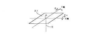
反射素子21は平面鏡からなる。反射素子21は、図2に示すようにθxおよびθy方向に回転可能とされている。θxは、反射素子21における望遠鏡部11の光軸Cとの交点Oを通るX軸を中心とする回転方向の傾き角である。θyは、交点Oを通るX軸に垂直なY軸を中心とする回転方向の傾き角である。
The
制御装置23は、CPU43、メモリ45を有している。制御装置23は、光源装置19、反射素子21を制御する。また、撮像素子13からの画像信号を入力し光学性能の評価処理を行う。
The
以下、上述した光学性能評価装置の動作を、図3に示すフローチャートを用いて説明する。 The operation of the above-described optical performance evaluation apparatus will be described below using the flowchart shown in FIG.
ステップS1:制御装置23のCPU43は、光源装置19の光源25を点灯する。光源25には、例えば白色光が使用される。光源25の光は、ピンホール27a、コリメータ29を通り形状可変鏡31で反射される。反射された光は、ビームスプリッタ33を通り、ダイバージャレンズ35により被検光学系である望遠鏡部11の焦点面FPに集光される。集光した光束は、望遠鏡部11を実際の使用時と逆の方向(図1に実線で示す)に導入され、副鏡17および主鏡15で反射され略平行光になる。平行光となった光束は、反射素子21で反射され、望遠鏡部11を使用時の方向(図1に二点鎖線で示す)に進行する。そして、焦点面FPに焦点を結ぶ。
Step S1: The CPU 43 of the
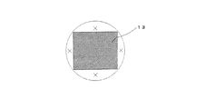
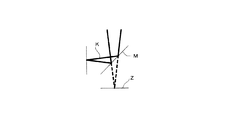
望遠鏡部11に光を導入する像面には、図4に斜線で示すように撮像素子13が配置されている。光を導入する位置は、例えば図4の円内の×の位置に設定するのが望ましい。一般に光学系は軸対称系が用いられるのが普通なので、この位置を設定することにより像性能を保証することができる。なお、この位置を導入位置として設定することが困難な場合には、例えば図5に示すように、反射鏡Mにより光路Kを折り曲げて像面Zと同一の焦点位置にするようにしても良い。 On the image plane for introducing light into the telescope unit 11, an image sensor 13 is arranged as shown by hatching in FIG. 4. The position where light is introduced is preferably set at a position x in the circle of FIG. 4, for example. In general, an axially symmetric system is usually used for the optical system, so that the image performance can be guaranteed by setting this position. If it is difficult to set this position as the introduction position, for example, as shown in FIG. 5, the optical path K may be bent by the reflecting mirror M so as to have the same focal position as the image plane Z. .
ステップS2:CPU43は、反射素子21を駆動して反射光を焦点面FPの入射位置に反射させる。そして、望遠鏡部11に入射した光束と望遠鏡部11から出射される光束とが重なるような傾き角θxおよびθyに反射素子21の角度を設定する。光が元の光路に戻るように反射素子21の傾きを調整すると、光束は光源装置19のダイバージャレンズ35、ビームスプリッタ33を通りシャック・ハルトマンセンサ37に導かれる。
Step S2: The CPU 43 drives the
ステップS3:被検光学系である望遠鏡部11の波面状態を検出する。この検出は、光源装置19に配置されるシャック・ハルトマンセンサ37により行われる。シャック・ハルトマンセンサ37は、ビームスプリッタ33から入射された光束をマイクロレンズアレイ39を介して撮像素子41に導く。撮像素子41で検出された画像は制御装置23に出力され波面状態が求められる。この波面状態は、導入した光が元の光路に戻るように反射素子21の傾きを調整しているため、往復の光路の波面収差を含んでいる。従って、この波面収差の半分の値が往路の波面収差になる。
Step S3: The wavefront state of the telescope unit 11 which is a test optical system is detected. This detection is performed by the Shack-
ステップS4:光源装置19の光源25からの光の波面状態を補正する。この補正は、形状可変鏡31により行われる。CPU43は、求められた波面状態に基づいて形状可変鏡31に信号を出力する。そして、望遠鏡部11の波面収差および反射素子21の形状誤差をキャンセルするような波面が得られるように形状可変鏡31を制御する。より具体的には、ステップS3で検出される波面収差は、往復の光路の波面収差を含んでいるため、この波面収差の1/2の波面収差をキャンセルできるような波面が得られるように形状可変鏡31を制御する。なお、望遠鏡部11の射出瞳、形状可変鏡31、シャック・ハルトマンセンサ37のマイクロレンズアレイ39は精度よく波面収差を検出し補正するために互いに共役関係にある。
Step S4: The wavefront state of the light from the
ステップS5:CPU43は、撮像素子13の所定位置に光が導かれるように反射素子21を駆動する。所定位置として、例えば図6に示すように撮像素子13の中央A、四隅の×で示す位置B,C,D,Eが選択されている。CPU43は、先ず、例えば撮像素子13の中央の位置Aに光が導かれるように反射素子21を駆動する。これにより撮像素子13の位置Aには、望遠鏡部11により広がった点像(PSF)が形成される。撮像素子13の所定位置A,B,C,D,Eに対する反射素子21の傾き角θx、θyは、撮像素子13の所定画素の信号より設定することで、所定位置A,B,C,D,Eに光を導くことができる。
Step S <b> 5: The CPU 43 drives the
ステップS6:CPU43は、反射素子21を走査して撮像素子13から点像をデータとして取得する。より具体的には、撮像素子13の傾き角θx、θyをステップ走査または連続走査して点像のプロファイルを取得する。
Step S6: The CPU 43 scans the
ステップS7:選択された全ての位置を測定していない場合には、残りの位置に対してステップS5およびステップS6の動作を行う。 Step S7: If not all the selected positions have been measured, the operations of Step S5 and Step S6 are performed on the remaining positions.
ステップS8:ステップS7において全ての位置を測定した後、ステップS6で得られたデータを計算処理して光学特性を評価する。例えば計算処理によりMTFやその他の特性を評価することができる。 Step S8: After all positions are measured in step S7, the data obtained in step S6 is calculated and evaluated for optical characteristics. For example, MTF and other characteristics can be evaluated by calculation processing.
上述した光学性能評価装置では、シャック・ハルトマンセンサ37により望遠鏡部11の波面状態を検出し、検出された波面状態に基づいて形状可変鏡31を制御し、微小光源25からの光の波面状態を補正するようにしたので、被検光学系である望遠鏡部11の光学性能を高精度で評価することができる。
In the optical performance evaluation device described above, the wavefront state of the telescope unit 11 is detected by the Shack-
(第2の実施形態)
以下、本発明の光学性能評価装置の第2の実施形態を説明する。なお、この実施形態において第1の実施形態と同一の要素には同一の符号を付して詳細な説明を省略する。
(Second Embodiment)
Hereinafter, a second embodiment of the optical performance evaluation apparatus of the present invention will be described. In this embodiment, the same elements as those in the first embodiment are denoted by the same reference numerals, and detailed description thereof is omitted.
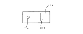
この実施形態では、被検光学系である望遠鏡の撮像素子に、例えば図7に示すような1次元ラインセンサからなる撮像素子13Aが用いられている。この撮像素子13Aは、多数の画素Gが直線状に形成されている。また、マスク部材27Aには、例えば図8に示すように、ピンホール27aおよびスリット27bが形成されている。マスク部材27Aは、ピンホール27aとスリット27bとの位置を切り替え可能に構成されている。マスク部材27Aはスリット27bをステップ走査または連続走査可能に構成されている。光源25には、白色光が用いられている。
In this embodiment, for example, an image sensor 13A including a one-dimensional line sensor as shown in FIG. 7 is used as an image sensor of a telescope that is a test optical system. In the imaging element 13A, a large number of pixels G are formed in a straight line. Further, for example, as shown in FIG. 8, pinholes 27a and slits 27b are formed in the mask member 27A. The mask member 27A is configured such that the positions of the pinhole 27a and the slit 27b can be switched. The mask member 27A is configured such that the slit 27b can be step-scanned or continuously scanned. White light is used for the
図9は、この実施形態の光学性能評価装置の動作を示すフローチャートである。 FIG. 9 is a flowchart showing the operation of the optical performance evaluation apparatus of this embodiment.
ステップS1:CPU43は、マスク部材27Aをピンホール27aの位置に設定し光源25を点灯する。なお、ステップS2、ステップS3、ステップS4は、図3のステップS2、ステップS3、ステップS4に対応するため詳細な説明を省略する。
Step S1: The CPU 43 sets the mask member 27A at the position of the pinhole 27a and turns on the
ステップS5:CPU43は、マスク部材27Aをスリット27bの位置に設定する。 Step S5: The CPU 43 sets the mask member 27A at the position of the slit 27b.
ステップS6:CPU43は、撮像素子13Aの所定位置に光が導かれるように反射素子21を駆動する。所定位置として、例えば図7に示すように撮像素子13Aの中央および両側の×で示す位置A’,B’,C’が選択されている。そして、先ず、例えば撮像素子13Aの中央の位置A’に光が導かれるように反射素子21を駆動する。これにより撮像素子13Aには、望遠鏡部11により広がったスリット像(LSF)が形成される。
撮像素子13Aの所定位置A’,B’,C’に対する反射素子21の傾き角θx、θyは、撮像素子13Aの所定画素の信号より設定することで、所定位置A’,B’,C’に光を導くことができる。
Step S6: The CPU 43 drives the reflecting
The inclination angles θx and θy of the reflecting
ステップS7:CPU43は、スリット27bを走査して撮像素子13Aからスリット像をデータとして取得する。より具体的には、スリット27bの形成されるマスク部材27Aをステップ走査または連続走査してスリット像のプロファイルを取得する。 Step S7: The CPU 43 scans the slit 27b and acquires a slit image as data from the image sensor 13A. More specifically, the profile of the slit image is obtained by performing step scanning or continuous scanning on the mask member 27A in which the slit 27b is formed.
ステップS8:選択された全ての位置を測定していない場合には残りの位置に対してステップS6およびステップS7の動作を行う。 Step S8: When not all the selected positions are measured, the operations of Step S6 and Step S7 are performed on the remaining positions.
ステップS9:ステップS8において全ての位置を測定した後、ステップS7で得られたデータを計算処理して光学特性を評価する。例えば計算処理によりMTFやその他の特性を評価することができる。 Step S9: After all positions are measured in step S8, the data obtained in step S7 is calculated and evaluated for optical characteristics. For example, MTF and other characteristics can be evaluated by calculation processing.
この実施形態の光学性能評価装置では、マスク部材27Aのピンホール27aからの点光源を用いてシャック・ハルトマンセンサ37により被検光学系である望遠鏡部11の波面状態を検出するようにしたので、波面状態を確実に検出することができる。そして、マスク部材27Aのスリット27bを用いてスリット像を取得するようにしたので、1次元ラインセンサからなる撮像素子13Aを使用する場合にも、スリット像を容易,確実に得ることができる。すなわち、1次元ラインセンサからなる撮像素子13Aでは、撮像素子13A上に点光源を位置させることが非常に困難であるが、スリット光源は所定の長さを有しているため、スリットを撮像素子13Aの画素G上に位置させることが比較的容易である。
(実施形態の補足事項)
以上、本発明を上述した実施形態によって説明してきたが、本発明の技術的範囲は上述した実施形態に限定されるものではなく、例えば、以下のような形態でも良い。
In the optical performance evaluation apparatus of this embodiment, the wavefront state of the telescope unit 11 that is the optical system to be detected is detected by the Shack-
(Supplementary items of the embodiment)
As mentioned above, although this invention was demonstrated by embodiment mentioned above, the technical scope of this invention is not limited to embodiment mentioned above, For example, the following forms may be sufficient.
(1)上述した実施形態では、被検光学系を望遠鏡にした例について説明したが、例えば、カメラ等の光学機器の光学系であっても良い。 (1) In the above-described embodiment, the example in which the optical system to be tested is a telescope has been described. However, for example, an optical system of an optical device such as a camera may be used.
(2)上述した第1の実施形態では、マスク部材27にピンホール27aを形成した例について説明したが、例えばレーザ光を使用する場合には、必ずしもマスク部材27Aを使用する必要はない。
(2) In the first embodiment described above, the example in which the pinhole 27a is formed in the
(3)上述した第2の実施形態では、マスク部材27Aのスリット27bを走査して撮像素子13Aからスリット像を取得した例について説明したが、反射素子21を走査してスリット像を取得するようにしても良い。
(3) In the second embodiment described above, the example in which the slit image is obtained from the imaging element 13A by scanning the slit 27b of the mask member 27A has been described, but the slit image is obtained by scanning the
11…望遠鏡部、13…撮像素子、21…反射素子、19…光源装置、23…制御装置、25…光源、27…マスク部材、31…形状可変鏡、37…シャック・ハルトマンセンサ。 DESCRIPTION OF SYMBOLS 11 ... Telescope part, 13 ... Imaging element, 21 ... Reflective element, 19 ... Light source device, 23 ... Control apparatus, 25 ... Light source, 27 ... Mask member, 31 ... Shape variable mirror, 37 ... Shack-Hartmann sensor
Claims (4)
前記被検光学系を通過した光を偏向させて前記焦点面に導く反射素子とを有し、
前記光源装置は、
前記焦点面に微小光源からの光を集光させる照明光学系と、
前記被検光学系の波面状態を検出する検出手段と、
前記波面状態に基づいて前記微小光源からの光の波面状態を補正する補正手段とを有し、
前記補正手段によって波面状態を補正された光が、前記像側から前記被検光学系に入射されることを特徴とする光学性能評価装置。 A light source device for guiding light from the image side to a test optical system having an image sensor on the focal plane on the image side;
A reflective element that deflects light that has passed through the optical system to be tested and guides the light to the focal plane;
The light source device
An illumination optical system for condensing light from a micro light source on the focal plane;
Detecting means for detecting a wavefront state of the test optical system;
Correction means for correcting the wavefront state of the light from the minute light source based on the wavefront state ;
An optical performance evaluation apparatus , wherein the light whose wavefront state is corrected by the correction means is incident on the optical system to be examined from the image side .
前記微小光源は、点光源とスリット光源とに切り換え可能であることを特徴とする光学性能評価装置。 The optical performance evaluation apparatus according to claim 1,
The optical performance evaluation apparatus, wherein the minute light source can be switched between a point light source and a slit light source.
前記反射素子の反射角をステップ的または連続的に変更する第1の変更手段を有していることを特徴とする光学性能評価装置。 In the optical performance evaluation apparatus according to claim 1 or 2,
An optical performance evaluation apparatus comprising first changing means for changing the reflection angle of the reflecting element stepwise or continuously.
前記スリット光源の位置をステップ的または連続的に変更する第2の変更手段を有していることを特徴とする光学性能評価装置。 In the optical performance evaluation apparatus according to claim 2 ,
An optical performance evaluation apparatus comprising second changing means for changing the position of the slit light source stepwise or continuously.
Priority Applications (1)
| Application Number | Priority Date | Filing Date | Title |
|---|---|---|---|
| JP2009009941A JP5402011B2 (en) | 2009-01-20 | 2009-01-20 | Optical performance evaluation device |
Applications Claiming Priority (1)
| Application Number | Priority Date | Filing Date | Title |
|---|---|---|---|
| JP2009009941A JP5402011B2 (en) | 2009-01-20 | 2009-01-20 | Optical performance evaluation device |
Publications (2)
| Publication Number | Publication Date |
|---|---|
| JP2010169424A JP2010169424A (en) | 2010-08-05 |
| JP5402011B2 true JP5402011B2 (en) | 2014-01-29 |
Family
ID=42701727
Family Applications (1)
| Application Number | Title | Priority Date | Filing Date |
|---|---|---|---|
| JP2009009941A Active JP5402011B2 (en) | 2009-01-20 | 2009-01-20 | Optical performance evaluation device |
Country Status (1)
| Country | Link |
|---|---|
| JP (1) | JP5402011B2 (en) |
Families Citing this family (4)
| Publication number | Priority date | Publication date | Assignee | Title |
|---|---|---|---|---|
| FR2972051B1 (en) * | 2011-02-24 | 2013-08-16 | Thales Sa | SIMPLIFIED CONTROL BENCH OF SELF-CONTROLLED TELESCOPES AND TELESCOPES |
| CN104964810B (en) * | 2015-06-16 | 2017-07-25 | 苏州佳世达光电有限公司 | light source detecting system and method |
| CN106092516B (en) * | 2016-05-27 | 2019-09-17 | 海信集团有限公司 | The aging equipment of optical element |
| CN108871733B (en) * | 2018-05-08 | 2020-04-07 | 中国科学院国家天文台南京天文光学技术研究所 | Near-field detection device of large-caliber optical system and measurement method thereof |
Family Cites Families (3)
| Publication number | Priority date | Publication date | Assignee | Title |
|---|---|---|---|---|
| JPH06250108A (en) * | 1993-02-22 | 1994-09-09 | Hitachi Ltd | Compensation optical device and astronomical telescope, optical data link, and laser working machine using same |
| EP1286208A4 (en) * | 2000-05-30 | 2003-08-13 | Mitsubishi Electric Corp | Image sensor |
| JP4140684B2 (en) * | 2000-11-28 | 2008-08-27 | 三菱電機株式会社 | Optical system deviation estimation apparatus, optical system deviation adjustment apparatus, optical system deviation estimation method, and optical system deviation adjustment method |
-
2009
- 2009-01-20 JP JP2009009941A patent/JP5402011B2/en active Active
Also Published As
| Publication number | Publication date |
|---|---|
| JP2010169424A (en) | 2010-08-05 |
Similar Documents
| Publication | Publication Date | Title |
|---|---|---|
| RU2008134018A (en) | WAVE SEQUENCE FRONT SENSOR | |
| ATE314671T1 (en) | AUTOFOCUSING DEVICE FOR AN OPTICAL DEVICE | |
| US10422861B2 (en) | Electro-optical distance measuring instrument | |
| JP2019133176A (en) | Deep ultraviolet, continuous wave laser, system, and method | |
| KR102052757B1 (en) | Optical monitoring device for an imaging system | |
| JP5402011B2 (en) | Optical performance evaluation device | |
| CN109416507A (en) | Optical system and the method for using this system compensation defects on mask | |
| KR102084457B1 (en) | Optical system intended to measure brdf, bsdf and btdf | |
| JP6328612B2 (en) | Guide star generation | |
| JP2005241607A (en) | Apparatus for measuring angle | |
| JP2009288075A (en) | Aberration measuring device and aberration measuring method | |
| US9442006B2 (en) | Method and apparatus for measuring the shape of a wave-front of an optical radiation field | |
| JP5511632B2 (en) | Laser irradiation device | |
| JP2007033653A (en) | Focus detection device and imaging apparatus using the same | |
| US9851557B2 (en) | Optical systems including lens assemblies and methods of imaging fields of view using such optical systems | |
| JP4721802B2 (en) | Automatic optical axis correction method for telecentric optical system, automatic optical axis correction telecentric optical apparatus, and exposure apparatus | |
| JP6255490B2 (en) | Scanning device | |
| KR100790706B1 (en) | Device for detecting focal lenghth of lenses | |
| JP7241986B2 (en) | WAVEFRONT MEASUREMENT DEVICE AND WAVEFRONT MEASUREMENT METHOD | |
| JP2008107274A (en) | Device for measuring focal position | |
| JP2006118944A (en) | Evaluation device of lens | |
| JP2009288076A (en) | Aberration measuring device | |
| JP2006042921A (en) | Eye refracting power measuring apparatus | |
| US6750436B2 (en) | Focus error detection apparatus and method having dual focus error detection path | |
| US6329634B1 (en) | Workpiece irradiation system |
Legal Events
| Date | Code | Title | Description |
|---|---|---|---|
| A621 | Written request for application examination |
Free format text: JAPANESE INTERMEDIATE CODE: A621 Effective date: 20120118 |
|
| A521 | Request for written amendment filed |
Free format text: JAPANESE INTERMEDIATE CODE: A523 Effective date: 20120907 |
|
| A977 | Report on retrieval |
Free format text: JAPANESE INTERMEDIATE CODE: A971007 Effective date: 20130423 |
|
| A131 | Notification of reasons for refusal |
Free format text: JAPANESE INTERMEDIATE CODE: A131 Effective date: 20130514 |
|
| A521 | Request for written amendment filed |
Free format text: JAPANESE INTERMEDIATE CODE: A523 Effective date: 20130709 |
|
| TRDD | Decision of grant or rejection written | ||
| A01 | Written decision to grant a patent or to grant a registration (utility model) |
Free format text: JAPANESE INTERMEDIATE CODE: A01 Effective date: 20131001 |
|
| A61 | First payment of annual fees (during grant procedure) |
Free format text: JAPANESE INTERMEDIATE CODE: A61 Effective date: 20131014 |
|
| R150 | Certificate of patent or registration of utility model |
Ref document number: 5402011 Country of ref document: JP Free format text: JAPANESE INTERMEDIATE CODE: R150 |
|
| R250 | Receipt of annual fees |
Free format text: JAPANESE INTERMEDIATE CODE: R250 |
|
| R250 | Receipt of annual fees |
Free format text: JAPANESE INTERMEDIATE CODE: R250 |
|
| R250 | Receipt of annual fees |
Free format text: JAPANESE INTERMEDIATE CODE: R250 |
|
| R250 | Receipt of annual fees |
Free format text: JAPANESE INTERMEDIATE CODE: R250 |
|
| R250 | Receipt of annual fees |
Free format text: JAPANESE INTERMEDIATE CODE: R250 |
|
| R250 | Receipt of annual fees |
Free format text: JAPANESE INTERMEDIATE CODE: R250 |
|
| R250 | Receipt of annual fees |
Free format text: JAPANESE INTERMEDIATE CODE: R250 |
|
| R250 | Receipt of annual fees |
Free format text: JAPANESE INTERMEDIATE CODE: R250 |