JP5392005B2 - Infrared imaging apparatus and infrared imaging method - Google Patents
Infrared imaging apparatus and infrared imaging method Download PDFInfo
- Publication number
- JP5392005B2 JP5392005B2 JP2009247765A JP2009247765A JP5392005B2 JP 5392005 B2 JP5392005 B2 JP 5392005B2 JP 2009247765 A JP2009247765 A JP 2009247765A JP 2009247765 A JP2009247765 A JP 2009247765A JP 5392005 B2 JP5392005 B2 JP 5392005B2
- Authority
- JP
- Japan
- Prior art keywords
- pixel
- connected image
- infrared
- image signal
- bolometers
- Prior art date
- Legal status (The legal status is an assumption and is not a legal conclusion. Google has not performed a legal analysis and makes no representation as to the accuracy of the status listed.)
- Active
Links
- 238000003331 infrared imaging Methods 0.000 title claims description 34
- 238000000034 method Methods 0.000 title claims description 18
- 230000002093 peripheral effect Effects 0.000 claims description 6
- 230000003321 amplification Effects 0.000 description 3
- 238000006243 chemical reaction Methods 0.000 description 3
- 238000003199 nucleic acid amplification method Methods 0.000 description 3
- 230000007423 decrease Effects 0.000 description 2
- 238000010586 diagram Methods 0.000 description 1
- 230000000694 effects Effects 0.000 description 1
Images

Landscapes
- Radiation Pyrometers (AREA)
- Solid State Image Pick-Up Elements (AREA)
- Transforming Light Signals Into Electric Signals (AREA)
- Photometry And Measurement Of Optical Pulse Characteristics (AREA)
Description
本発明は、赤外線撮像装置および赤外線撮像方法に関する。 The present invention relates to an infrared imaging device and an infrared imaging method.
赤外線撮像装置においては、高いS/N比(Signal-to-Noise Ratio)が要求されている。例えば、ボロメータ型の赤外線撮像装置のノイズは、画素ごとに設けられたボロメータが持つ1/fノイズが支配的であり、1/fノイズは、ボロメータの体積に反比例して小さくなることが知られている(特許文献1参照)。 In an infrared imaging device, a high S / N ratio (Signal-to-Noise Ratio) is required. For example, it is known that the noise of a bolometer-type infrared imaging device is dominated by 1 / f noise of a bolometer provided for each pixel, and the 1 / f noise decreases in inverse proportion to the volume of the bolometer. (See Patent Document 1).
ところが、赤外線撮像装置において、S/N比を高めるために、赤外線センサの画素サイズを大きくしようとすると、赤外線センサを収容するパッケージサイズが大きくなるなどの問題から、解像度が落ちてしまうという問題がある。 However, in an infrared imaging device, when an attempt is made to increase the pixel size of the infrared sensor in order to increase the S / N ratio, there is a problem that the resolution is lowered due to a problem that the package size for accommodating the infrared sensor is increased. is there.
逆に、解像度を上げようとすると、赤外線センサの画素サイズを小さくする必要があり、その場合、S/N比が落ちてしまうという問題がある。 On the other hand, when trying to increase the resolution, it is necessary to reduce the pixel size of the infrared sensor. In this case, there is a problem that the S / N ratio decreases.
上述のように、赤外線撮像装置においては、高解像度でかつ高S/N比の画像を取得することが困難であるという課題がある。 As described above, the infrared imaging device has a problem that it is difficult to acquire an image with a high resolution and a high S / N ratio.
そこで、本発明の目的は、上記の課題を解決し、高解像度でかつ高S/N比の画像を取得することができる赤外線撮像装置および赤外線撮像方法を提供することにある。 Accordingly, an object of the present invention is to provide an infrared imaging device and an infrared imaging method capable of solving the above-described problems and acquiring an image with a high resolution and a high S / N ratio.
本発明の赤外線撮像装置は、
被写体の撮影時に、被写体からの赤外光を集光する赤外線レンズと、
画素ごとに設けられたボロメータを具備し、前記赤外線レンズにて集光された赤外光を画像信号としてボロメータにより1画素ずつ検知する赤外線センサと、
N(Nは2以上の自然数)直列N並列にN×N個のボロメータを接続し、N×N個のボロメータで検知されたN×N画素分の画像信号を連結画像信号として読出し、当該読出し動作を所定の時間間隔で1画素ずつシフトさせながら繰り返す読出し処理部と、
前記連結画像信号による連結画像ごとに、当該連結画像の連結画像信号と当該連結画像に重なり合う周辺の連結画像の連結画像信号とを用いて超解像処理を行う超解像処理部と、を有する。
The infrared imaging device of the present invention is
An infrared lens that collects infrared light from the subject when shooting the subject;
An infrared sensor that includes a bolometer provided for each pixel, and that detects infrared light collected by the infrared lens one pixel at a time using the bolometer as an image signal;
N (N is a natural number equal to or greater than 2) N × N bolometers are connected in series N in parallel, and N × N pixel image signals detected by the N × N bolometers are read out as connected image signals. A readout processing unit that repeats the operation while shifting the operation by one pixel at a predetermined time interval;
A super-resolution processing unit that performs super-resolution processing for each connected image by the connected image signal using a connected image signal of the connected image and a connected image signal of a peripheral connected image that overlaps the connected image. .
本発明の赤外線撮像方法は、
赤外線撮像装置による赤外線撮像方法であって、
被写体の撮影時に、被写体からの赤外光を赤外線レンズにより集光するステップと、
赤外線センサの画素ごとに設けられたボロメータにより、前記赤外線レンズにて集光された赤外光を画像信号として1画素ずつ検知するステップと、
N(Nは2以上の自然数)直列N並列にN×N個のボロメータを接続し、N×N個のボロメータで検知されたN×N画素分の画像信号を連結画像信号として読出し、当該読出し動作を所定の時間間隔で1画素ずつシフトさせながら繰り返す読出しステップと、
前記連結画像信号による連結画像ごとに、当該連結画像の連結画像信号と当該連結画像に重なり合う周辺の連結画像の連結画像信号とを用いて超解像処理を行うステップと、を有する。
Infrared imaging method of the present invention,
An infrared imaging method using an infrared imaging device,
Condensing infrared light from the subject with an infrared lens when photographing the subject;
Detecting the infrared light collected by the infrared lens as an image signal one pixel at a time using a bolometer provided for each pixel of the infrared sensor;
N (N is a natural number equal to or greater than 2) N × N bolometers are connected in series N in parallel, and N × N pixel image signals detected by the N × N bolometers are read out as connected image signals. A readout step of repeating the operation while shifting the pixel one pixel at a predetermined time interval;
For each connected image based on the connected image signal, super-resolution processing is performed using the connected image signal of the connected image and the connected image signal of the peripheral connected image overlapping the connected image.
本発明によれば、赤外線撮像装置において、高解像度でかつ高S/N比の画像を取得することができるという効果が得られる。 According to the present invention, an effect that an image with high resolution and a high S / N ratio can be acquired in an infrared imaging device can be obtained.
以下に、本発明を実施するための形態について図面を参照して説明する。 EMBODIMENT OF THE INVENTION Below, the form for implementing this invention is demonstrated with reference to drawings.
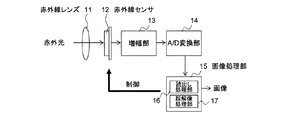
図1に示すように、本実施形態の赤外線撮像装置は、赤外線レンズ11と、赤外線センサ12と、増幅部13と、A/D変換部14と、画像処理部15と、を有している。また、画像処理部15は、読出し処理部16と、超解像処理部17と、を有している。
As shown in FIG. 1, the infrared imaging device of the present embodiment includes an infrared lens 11, an infrared sensor 12, an
赤外線レンズ11は、被写体の撮影時に、被写体からの赤外光を集光する。 The infrared lens 11 condenses infrared light from the subject when photographing the subject.
赤外線センサ12は、画素ごとに設けられたボロメータを有し、赤外線レンズ11にて集光された赤外光を画像信号としてボロメータにより1画素ずつ検知する。 The infrared sensor 12 has a bolometer provided for each pixel, and detects infrared light collected by the infrared lens 11 pixel by pixel using the bolometer as an image signal.
赤外線センサ12にて検知された画像信号は、画像処理部15の読出し処理部16の制御の元で読出され、増幅部13にて増幅され、A/D変換部14にてデジタル信号に変換された後、画像処理部15から不図示の表示装置へと出力される。
The image signal detected by the infrared sensor 12 is read under the control of the
以下、本実施形態の赤外線撮像装置の動作について説明する。
(1)画素の読出し処理
まず、本実施形態の赤外線撮像装置の画素の読出し処理を、関連する赤外線撮像装置と対比しながら説明する。
Hereinafter, the operation of the infrared imaging device of the present embodiment will be described.
(1) Pixel Reading Process First, the pixel reading process of the infrared imaging apparatus of the present embodiment will be described in comparison with the related infrared imaging apparatus.
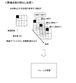
図2を参照すると、関連する赤外線撮像装置においては、1つのボロメータで検知された1画素分の画像信号を読出し、この読出し動作を所定の時間間隔で1画素ずつシフトさせながら繰り返すことで、全画素を読出す。 Referring to FIG. 2, in the related infrared imaging apparatus, an image signal for one pixel detected by one bolometer is read, and this reading operation is repeated while shifting one pixel at a time interval, Read the pixel.
これに対して、図3を参照すると、本実施形態の赤外線撮像装置においては、読出し処理部16は、2直列2並列に4個のボロメータを接続し、4個のボロメータで検知された4画素分の画像信号を連結画像信号として読出し、この読出し動作を所定の時間間隔で1画素ずつシフトさせながら繰り返すことで、全画素を読出す。
On the other hand, referring to FIG. 3, in the infrared imaging device of the present embodiment, the
このとき、4個のボロメータの等価回路は、図3に示すように、4個のボロメータが2直列2並列に接続された回路となる。1つのボロメータの抵抗値をRbとすると、この等価回路の全体抵抗値は、(2×Rb)/2=Rbとなり、図2と同値になる。 At this time, the equivalent circuit of the four bolometers is a circuit in which four bolometers are connected in two series and two in parallel as shown in FIG. If the resistance value of one bolometer is Rb, the total resistance value of this equivalent circuit is (2 × Rb) / 2 = Rb, which is the same value as in FIG.
なお、図2および図3においては、左端の最上部の画素から右方向に1画素ずつシフトし、右端の画素まで進んだら、1画素分下方向にシフトして左端の画素から右方向に1画素ずつシフトすることを繰り返すという順序で画素の読出しを行っているが、画素を読出す順序はこれに限定されず、全画素を読出すことができれば、順序は問わない。 In FIGS. 2 and 3, the pixel is shifted one pixel at a time from the uppermost pixel at the left end to the right end pixel. When the pixel reaches the right end pixel, the pixel is shifted downward by one pixel and the pixel at the left end is shifted to the right by one. Pixels are read in the order of repeating shifting pixel by pixel, but the order of reading pixels is not limited to this, and the order is not limited as long as all pixels can be read.
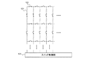
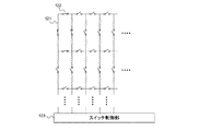
ここで、本実施形態の上記読出し動作の具体的な実現手段を、図4Aおよび図4Bを参照して説明する。図4Aおよび図4Bは、赤外線センサ12の概略構成を示している。 Here, specific means for realizing the read operation of the present embodiment will be described with reference to FIGS. 4A and 4B. 4A and 4B show a schematic configuration of the infrared sensor 12.
図4Aおよび図4Bを参照すると、赤外線センサ12は、画素ごとに設けられたボロメータ121と、ボロメータ121間に配置されたスイッチ122と、読出し処理部16の制御の元で、スイッチ122の開閉状態を制御するスイッチ制御部123と、を有する。
Referring to FIGS. 4A and 4B, the infrared sensor 12 includes a
例えば、図3の読出し時刻nにおいては、スイッチ制御部123は、図4Aのように、画像信号を読み出す4個の画素の4個のボロメータ間に配置されたスイッチ122を閉状態にし、その他のスイッチ122を開状態にする。
For example, at the readout time n in FIG. 3, the
また、図3の読出し時刻n+1においては、スイッチ制御部123は、図4Bのように、画像信号を読み出す4個の画素の4個のボロメータ間に配置されたスイッチ122を閉状態にし、その他のスイッチ122を開状態にする。
(2)超解像処理
本実施形態において、上記のように読出した連結画像信号による画像は、4画素分の画像を連結した連結画像であるため、解像度が低い低解像度画像となる。
Further, at the readout time n + 1 in FIG. 3, the
(2) Super-resolution processing In the present embodiment, the image based on the connected image signal read out as described above is a connected image obtained by connecting the images for four pixels, and thus becomes a low-resolution image with low resolution.
そこで、本実施形態においては、超解像処理部17は、連結画像信号を不図示のメモリに蓄積しておき、連結画像ごとに、その連結画像の連結画像信号とその連結画像に重なり合う周辺の連結画像の連結画像信号とを用いて超解像処理を行うことにより、その連結画像の画素を1画素ずつ読出した時と同じ画素数に高解像度化する。
Therefore, in the present embodiment, the
なお、超解像処理は、公知の技術であり(例えば、「業界が注目!超解像技術について」、[平成21年10月21日検索]、インターネット<http://www.toshiba.co.jp/regza/detail/superresolution/resolution.html>)、本発明は公知の技術を利用できるため、超解像処理に関する詳細な説明を省略する。 The super-resolution processing is a known technique (for example, “Industry attention! Super-resolution technology”, [October 21, 2009 search], Internet <http://www.toshiba.co .jp / regza / detail / superresolution / resolution.html>), since a known technique can be used in the present invention, a detailed description of super-resolution processing is omitted.
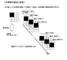
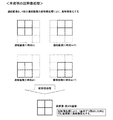
図5を参照すると、超解像処理部17は、例えば、図3の読出し時刻nにおいて連結画像信号を読出した連結画像1を高解像度化する場合、読出し時刻nにおいて読出した連結画像1の連結画像信号と、読出し時刻n+1において読出した連結画像2の連結画像信号と、読出し時刻mにおいて読出した連結画像3の連結画像信号と、読出し時刻m+1において読出した連結画像4の連結画像信号と、を用いて超解像処理を行う。
Referring to FIG. 5, for example, when the resolution of the connected image 1 read from the connected image signal at the read time n in FIG. 3 is increased, the
より具体的には、図6を参照すると、連結画像1が「A」という文字を表した画像である場合、連結画像1〜4の各々の連結画像信号を用いて超解像処理を行うことで、連結画像1の高解像度化が図れる。 More specifically, referring to FIG. 6, when the connected image 1 is an image representing the letter “A”, super-resolution processing is performed using each connected image signal of the connected images 1 to 4. Thus, the resolution of the connected image 1 can be increased.
上述したように本実施形態においては、読出し処理部16は、2直列2並列に4個のボロメータを接続し、4個のボロメータで検知された4画素分の画像信号を連結画像信号として読出し、当該読出し動作を所定の時間間隔で1画素ずつシフトさせながら繰り返し、また、超解像処理部17は、連結画像ごとに、当該連結画像の連結画像信号と当該連結画像に重なり合う周辺の連結画像の連結画像信号とを用いて超解像処理を行う。
As described above, in the present embodiment, the
このように、画像信号の読出し時に、4個のボロメータを2直列2並列に接続することで1/fノイズが低減されるため、高いS/N比が得ることができる。 As described above, when the image signal is read out, the 1 / f noise is reduced by connecting the four bolometers in two series and two in parallel, so that a high S / N ratio can be obtained.
また、4画素分の連結画像信号による連結画像の超解像処理を行うため、その連結画像の画素を1画素ずつ読出した時と同じ画素数に高解像度化することができる。さらに、超解像処理によりホワイトノイズも低減することができる。 Further, since the super-resolution processing of the connected image using the connected image signal for four pixels is performed, the resolution can be increased to the same number of pixels as when the pixels of the connected image are read out pixel by pixel. Furthermore, white noise can also be reduced by super-resolution processing.
したがって、赤外線撮像装置において、高解像度でかつ高S/N比の画像を取得することができるようになる。 Therefore, in the infrared imaging device, an image with high resolution and a high S / N ratio can be acquired.
なお、本実施形態においては、画像信号の読出し時に、2直列2並列に4個のボロメータを接続し、4個のボロメータで検知された4画素分の画像信号を連結画像信号として読出す構成について説明したが、本発明はこれに限定されず、N(Nは2以上の自然数)直列N並列にN×N個のボロメータを接続し、N×N個のボロメータで検知されたN×N画素分の画像信号を連結画像信号として読出す構成であればよい。 In the present embodiment, when reading out an image signal, four bolometers are connected in two series and two in parallel, and an image signal for four pixels detected by the four bolometers is read out as a connected image signal. Although described above, the present invention is not limited to this, and N (N is a natural number of 2 or more) N × N bolometers connected in series N in parallel, and N × N pixels detected by N × N bolometers It suffices if the image signal is read as a connected image signal.
11 赤外線レンズ
12 赤外線センサ
13 増幅部
14 A/D変換部
15 画像処理部
16 読出し処理部
17 超解像処理部
DESCRIPTION OF SYMBOLS 11 Infrared lens 12
Claims (4)
画素ごとに設けられたボロメータを具備し、前記赤外線レンズにて集光された赤外光を画像信号としてボロメータにより1画素ずつ検知する赤外線センサと、
N(Nは2以上の自然数)直列N並列にN×N個のボロメータを接続し、N×N個のボロメータで検知されたN×N画素分の画像信号を連結画像信号として読出し、当該読出し動作を所定の時間間隔で1画素ずつシフトさせながら繰り返す読出し処理部と、
前記連結画像信号による連結画像ごとに、当該連結画像の連結画像信号と当該連結画像に重なり合う周辺の連結画像の連結画像信号とを用いて超解像処理を行う超解像処理部と、を有する赤外線撮像装置。 An infrared lens that collects infrared light from the subject when shooting the subject;
An infrared sensor that includes a bolometer provided for each pixel, and that detects infrared light collected by the infrared lens one pixel at a time using the bolometer as an image signal;
N (N is a natural number equal to or greater than 2) N × N bolometers are connected in series N in parallel, and N × N pixel image signals detected by the N × N bolometers are read out as connected image signals. A readout processing unit that repeats the operation while shifting the operation by one pixel at a predetermined time interval;
A super-resolution processing unit that performs super-resolution processing for each connected image by the connected image signal using a connected image signal of the connected image and a connected image signal of a peripheral connected image that overlaps the connected image. Infrared imaging device.
前記ボロメータ間に配置されたスイッチと、
前記読出し処理部の制御の元で、画像信号を読み出すN×N個の画素のN×N個のボロメータ間に配置されたスイッチを閉状態にし、その他のスイッチを開状態にするスイッチ制御部と、をさらに具備する、請求項1に記載の赤外線撮像装置。 The infrared sensor is
A switch disposed between the bolometers;
A switch control unit that closes a switch disposed between N × N bolometers of an N × N pixel that reads an image signal under the control of the readout processing unit, and that opens the other switches; The infrared imaging device according to claim 1, further comprising:
被写体の撮影時に、被写体からの赤外光を赤外線レンズにより集光するステップと、
赤外線センサの画素ごとに設けられたボロメータにより、前記赤外線レンズにて集光された赤外光を画像信号として1画素ずつ検知するステップと、
N(Nは2以上の自然数)直列N並列にN×N個のボロメータを接続し、N×N個のボロメータで検知されたN×N画素分の画像信号を連結画像信号として読出し、当該読出し動作を所定の時間間隔で1画素ずつシフトさせながら繰り返す読出しステップと、
前記連結画像信号による連結画像ごとに、当該連結画像の連結画像信号と当該連結画像に重なり合う周辺の連結画像の連結画像信号とを用いて超解像処理を行うステップと、を有する赤外線撮像方法。 An infrared imaging method using an infrared imaging device,
Condensing infrared light from the subject with an infrared lens when photographing the subject;
Detecting the infrared light collected by the infrared lens as an image signal one pixel at a time using a bolometer provided for each pixel of the infrared sensor;
N (N is a natural number equal to or greater than 2) N × N bolometers are connected in series N in parallel, and N × N pixel image signals detected by the N × N bolometers are read out as connected image signals. A readout step of repeating the operation while shifting the pixel one pixel at a predetermined time interval;
Performing a super-resolution process for each connected image based on the connected image signal, using a connected image signal of the connected image and a connected image signal of a peripheral connected image that overlaps the connected image.
画像信号を読み出すN×N個の画素のN×N個のボロメータ間に配置されたスイッチを閉状態にし、その他のスイッチを開状態にする、請求項3に記載の赤外線撮像方法。 In the reading step,
The infrared imaging method according to claim 3, wherein a switch disposed between N × N bolometers of N × N pixels for reading out an image signal is closed, and the other switches are opened.
Priority Applications (1)
| Application Number | Priority Date | Filing Date | Title |
|---|---|---|---|
| JP2009247765A JP5392005B2 (en) | 2009-10-28 | 2009-10-28 | Infrared imaging apparatus and infrared imaging method |
Applications Claiming Priority (1)
| Application Number | Priority Date | Filing Date | Title |
|---|---|---|---|
| JP2009247765A JP5392005B2 (en) | 2009-10-28 | 2009-10-28 | Infrared imaging apparatus and infrared imaging method |
Publications (2)
| Publication Number | Publication Date |
|---|---|
| JP2011095044A JP2011095044A (en) | 2011-05-12 |
| JP5392005B2 true JP5392005B2 (en) | 2014-01-22 |
Family
ID=44112129
Family Applications (1)
| Application Number | Title | Priority Date | Filing Date |
|---|---|---|---|
| JP2009247765A Active JP5392005B2 (en) | 2009-10-28 | 2009-10-28 | Infrared imaging apparatus and infrared imaging method |
Country Status (1)
| Country | Link |
|---|---|
| JP (1) | JP5392005B2 (en) |
Cited By (1)
| Publication number | Priority date | Publication date | Assignee | Title |
|---|---|---|---|---|
| US12181344B2 (en) | 2020-12-24 | 2024-12-31 | Samsung Electronics Co., Ltd. | Thermal infrared detector |
Family Cites Families (2)
| Publication number | Priority date | Publication date | Assignee | Title |
|---|---|---|---|---|
| GB0202506D0 (en) * | 2002-02-02 | 2002-03-20 | Qinetiq Ltd | Reconfigurable detector array |
| JP2008076373A (en) * | 2006-09-22 | 2008-04-03 | Seiko Npc Corp | Infrared ray detector |
-
2009
- 2009-10-28 JP JP2009247765A patent/JP5392005B2/en active Active
Cited By (1)
| Publication number | Priority date | Publication date | Assignee | Title |
|---|---|---|---|---|
| US12181344B2 (en) | 2020-12-24 | 2024-12-31 | Samsung Electronics Co., Ltd. | Thermal infrared detector |
Also Published As
| Publication number | Publication date |
|---|---|
| JP2011095044A (en) | 2011-05-12 |
Similar Documents
| Publication | Publication Date | Title |
|---|---|---|
| CN101536491B (en) | Imaging device and imaging method | |
| JP4448888B2 (en) | Imaging apparatus and signal processing method of imaging apparatus | |
| JP2008193163A (en) | Solid-state imaging device | |
| JP2011097568A (en) | Image sensing apparatus | |
| CN105430361B (en) | Imaging method, imaging sensor, imaging device and electronic installation | |
| TW462178B (en) | Circuit architecture and method for switching sensor resolution | |
| JP2013236298A (en) | Imaging apparatus | |
| TW201204020A (en) | Imaging device and image processing device | |
| JP2010171666A (en) | Driving method of solid state imaging element, and solid state imaging element | |
| TW200924512A (en) | Image processing device and image processing method | |
| JP5217213B2 (en) | Imaging apparatus and program | |
| JP5392005B2 (en) | Infrared imaging apparatus and infrared imaging method | |
| JP5829122B2 (en) | Imaging apparatus and evaluation value generation apparatus | |
| WO2017138200A1 (en) | Imaging device and method for controlling imaging device | |
| JP4929584B2 (en) | Signal processing method, signal processing apparatus, and semiconductor device for detecting physical quantity distribution | |
| JP4326239B2 (en) | Electronic imaging system and method for improving image quality in an electronic imaging system | |
| JP2008172606A (en) | Solid-state imaging device and camera system | |
| JP2007081991A5 (en) | ||
| JP5398610B2 (en) | Solid-state electronic imaging device and operation control method thereof | |
| JP6448219B2 (en) | Imaging apparatus and control method thereof | |
| JP2006005500A (en) | Imaging device, imaging method, and imaging device | |
| JP4807075B2 (en) | Imaging device and defective pixel correction method thereof | |
| KR100931859B1 (en) | Wafer Inspection Camera | |
| JP2008227255A (en) | Electronic device with charge detection amplifier | |
| JP4229234B2 (en) | Digital camera |
Legal Events
| Date | Code | Title | Description |
|---|---|---|---|
| A621 | Written request for application examination |
Free format text: JAPANESE INTERMEDIATE CODE: A621 Effective date: 20120912 |
|
| A977 | Report on retrieval |
Free format text: JAPANESE INTERMEDIATE CODE: A971007 Effective date: 20130710 |
|
| TRDD | Decision of grant or rejection written | ||
| A01 | Written decision to grant a patent or to grant a registration (utility model) |
Free format text: JAPANESE INTERMEDIATE CODE: A01 Effective date: 20130917 |
|
| A61 | First payment of annual fees (during grant procedure) |
Free format text: JAPANESE INTERMEDIATE CODE: A61 Effective date: 20130930 |
|
| R150 | Certificate of patent or registration of utility model |
Ref document number: 5392005 Country of ref document: JP Free format text: JAPANESE INTERMEDIATE CODE: R150 Free format text: JAPANESE INTERMEDIATE CODE: R150 |