JP5385722B2 - Interface circuit - Google Patents
Interface circuit Download PDFInfo
- Publication number
- JP5385722B2 JP5385722B2 JP2009190218A JP2009190218A JP5385722B2 JP 5385722 B2 JP5385722 B2 JP 5385722B2 JP 2009190218 A JP2009190218 A JP 2009190218A JP 2009190218 A JP2009190218 A JP 2009190218A JP 5385722 B2 JP5385722 B2 JP 5385722B2
- Authority
- JP
- Japan
- Prior art keywords
- data
- protocol
- signal
- mode
- clock
- Prior art date
- Legal status (The legal status is an assumption and is not a legal conclusion. Google has not performed a legal analysis and makes no representation as to the accuracy of the status listed.)
- Expired - Fee Related
Links
Images


Landscapes
- Information Transfer Systems (AREA)
- Communication Control (AREA)
Description
本発明は、各種の電子装置で使用される2種類の標準プロトコルを自動的に切り換える機能を有するインターフェース回路などに関する。 The present invention relates to an interface circuit having a function of automatically switching between two types of standard protocols used in various electronic devices.
図5は、モトローラ社によって開発された汎用のSPIインターフェースを用いて、マスタ装置(図示せず)との間でシリアル通信ができるスレーブ装置である電子装置100のブロック図である。
このスレーブ装置100は、図5に示すように、選択信号線102、クロック線106、およびデータ線104と接続されるようになっている。選択信号線102には、マスタ装置からスレーブ装置100を選択するための選択信号CSBが供給される。クロック線106には、マスタ装置からシリアルクロックSCLが供給される。データ線104は、マスタ装置との間で双方向の通信をするときに、データSDAの授受に使用される。
FIG. 5 is a block diagram of the
The
このような構成のスレーブ装置100では、図6に示すようなタイミングで通信が行われる。すなわち、選択信号CSBが「ハイレベル」から「ローレベル」に遷移後に、クロックSCLに同期してデータSDAが供給される。
図7は、フィリップス社によって開発された汎用のI2Cインターフェースを用いて、マスタ装置(図示せず)との間で双方向の通信を行うことができるスレーブ装置である電子装置300のブロック図である。
In the
FIG. 7 is a block diagram of an
このスレーブ装置300は、図7に示すように、クロック線304およびデータ線302からなる双方向バスと接続されるようになっている。クロック線304には、マスタ装置からシリアルクロックSCLが供給される。データ線302は、マスタ装置との間で双方向の通信をするときに、データSDAの授受に使用される。
このような構成のスレーブ装置300では、図8に示すようなタイミングで通信が行われる。
As shown in FIG. 7, the
In the
すなわち、この通信では、通信開始はデータ転送開始「START」、その終了はデータ転送終了「STOP」という固有の状態が発生する。そして、データ転送開始「START」は、クロックSCLが「ハイレベル」でデータSDAが「ハイレベル」から「ローレベル」への遷移である。一方、データ転送終了「STOP」は、クロックSCLが「ハイレベル」でデータSDAが「ローレベル」から「ハイレベル」への遷移である。データ転送開始「START」後に、クロックSCLに同期してデータSDAが供給される。 That is, in this communication, a unique state occurs in which the communication start is the data transfer start “START” and the end is the data transfer end “STOP”. The data transfer start “START” is a transition from the clock SCL to “high level” and the data SDA from “high level” to “low level”. On the other hand, the data transfer completion “STOP” is a transition from the clock SCL to “high level” and the data SDA from “low level” to “high level”. After the start of data transfer “START”, data SDA is supplied in synchronization with the clock SCL.
ここで、SPIインターフェースとI2Cインターフェースの両方の機能を持ち、これらを自動的に切り換える電子装置、およびその機能の自動切り換え方法が知られている(例えば、特許文献1参照)。
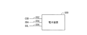
図9は、特許文献1に記載された、従来のインターフェース・プロトコルを自動的に切り換える電子装置のブロック図である。
この電子装置500は、選択信号線502、クロック線506、およびデータ線504と接続されるようになっている。
Here, an electronic apparatus having both functions of an SPI interface and an I2C interface and automatically switching between these functions and an automatic switching method of the functions are known (for example, see Patent Document 1).
FIG. 9 is a block diagram of an electronic device described in Patent Document 1 that automatically switches a conventional interface protocol.
The
選択信号線502には、マスタ装置からスレーブ装置である電子装置500を選択するための選択信号CSBが供給される。クロック線506には、マスタ装置からクロックSCLが供給される。データ線504は、マスタ装置との間で双方向の通信をするときに、データSDAの授受に使用される。
このような電子装置500では、選択信号CSBの極性、言い換えると選択信号CSBのレベルで、SPIインターフェースとI2Cインターフェースの機能を自動的に切り換えるように構成されている。すなわち、選択信号CSBが「ローレベル」ではSPIインターフェースが選択され、選択信号CSBが「ハイレベル」ではI2Cインターフェースが選択される。
The
Such an
図10は、特許文献1に記載された2つのプロトコルの切り換える方法に関するデータ送受のフローチャートであり、電子装置500の動作手順について以下に説明する。
ステップS1において、マスタ装置が選択信号502上とデータ線504上とクロック線506上に「ハイレベル」を供給することで、電子装置500はデフォルト(標準動作)としてインターフェースをI2Cモードに設定する。ステップS2において、電子装置500は入力信号についてインターフェースを監視する。ステップS3において、電子装置500は、選択信号線502上の選択信号CSBの「ハイレベル」から「ローレベル」への遷移の有無を検出する。
FIG. 10 is a flowchart of data transmission / reception regarding a method of switching between two protocols described in Patent Document 1, and an operation procedure of the
In step S1, the master apparatus supplies “high level” on the
ステップS3において、選択信号CSBの「ローレベル」への遷移が検出されないときには、ステップS8に進む。ステップS8では、電子装置500は、データ線504上のデータSDAについてデータ転送開始「START」に遷移があるか否かを判定する。この判定の結果、その遷移がない場合にはステップS2に戻り、その遷移がある場合にはステップS9に進む。ステップS9では、電子装置500はI2Cモードで読み出し動作や書き込み動作を実行し、その実行の終了後にステップS2に戻る。
If no transition of the selection signal CSB to “low level” is detected in step S3, the process proceeds to step S8. In step S8, the
一方、ステップS3において、選択信号CSBの「ローレベル」への遷移が検出されると、次のステップS4に進む。ステップS4では、電子装置500はインターフェースをSPIモードで動作するように設定する。ステップS5では、電子装置500は、SPIモードで読み出し動作や書き込み動作を実行する。電子装置500は、ステップS6において選択信号線502上の選択信号CSBの「ハイレベル」への遷移を検出すると、ステップS7でインターフェースをI2Cモードに設定して、ステップS2に戻る。
On the other hand, when the transition of the selection signal CSB to “low level” is detected in step S3, the process proceeds to the next step S4. In step S4, the
図9で示すような電子装置500をスレーブ装置としてマスタ装置との間で通信を行う通信システムでは、1つのマスタ装置で多数の電子装置のアクティブ/非アクティブを制御することが要求される。図11は、このような通信システムの一例を示すブロック図である。
図11の通信システムは、1つのマスタ装置702と、スレーブ装置として機能する4つの電子装置704、706、708、710とからなり、マスタ装置702がその4つの電子装置のうちの1つと選択的に双方向通信する。
In a communication system that performs communication with a master device using the
The communication system of FIG. 11 includes one
このため、マスタ装置702と4つの電子装置704、706、708、710とは、クロックSCLを転送する共通のクロック線720およびデータSDAを転送する共通のデータ線722で接続されている。また、マスタ装置702と電子装置704、706、708、710とは、独立の選択信号線724、726、728、730により接続されている。そして、マスタ装置702との間で行われるSPIプロトコルに基づく通信における電子装置704、706、708、710のうちの何れかのアクティブ/非アクティブの制御には、選択信号CSB1、CSB2、CSB3、CSB4が使用される。
Therefore, the
図12は、1つのマスタ装置802が2つの電子装置804、806と選択的に双方向の通信を行う通信システムのブロック図である。
この通信システムにおいて、マスタ装置802が電子装置804との間でSPIプロトコルに従ったデータ送受を行う場合、クロック線814上のクロックSCL、データ線812のデータSDA、および選択信号線810上の選択信号CSB1が使用される。選択信号線810上の選択信号CSB1が「ローレベル」で、選択信号線816上の選択信号CSB2が「ハイレベル」となる。
このとき、電子装置804はSPIインターフェースが設定され、電子装置806はI2Cインターフェースが設定された状態である。そして、電子装置804へのデータ線812上の送受データSDAとクロック線814上のクロックSCLは、電子装置806にも入力される。
FIG. 12 is a block diagram of a communication system in which one
In this communication system, when the
At this time, the SPI interface is set for the
このとき、選択信号CSB2が「ハイレベル」であって、クロックSCLが「ハイレベル」で送受データSDAが「ハイレベル」から「ローレベル」への遷移が行われると、電子装置806はI2Cインターフェースのデータ転送開始「START」を認識して(図8参照)、I2Cモードで読み出し動作や書き込み動作を開始する。
このように、クロックSCLと転送データSDAによって、電子装置806がI2Cモードで読み出し動作や書き込み動作を開始する誤動作を生じる。そしてさらに、電子装置804へのデータ送受が妨害される、という不具合が発生する。
At this time, when the selection signal CSB2 is “high level”, the clock SCL is “high level”, and the transmission / reception data SDA is changed from “high level” to “low level”, the
As described above, the clock SCL and the transfer data SDA cause a malfunction in which the
図12では、2つの電子装置を用いたデータ送受の例を示したが、このような誤動作は図11のように多数の電子装置を制御する場合にも同様である。
このような誤動作は、たとえば、電子装置806がデータ転送開始「START」を認識しないタイミング、つまりクロックSCLが「ハイレベル」で送受データSDAの「ハイレベル」から「ローレベル」への遷移が生じないようにマスタ装置802が信号を発行した場合であっても、起こりうる。この理由について、以下に図面を参照して説明する。
Although FIG. 12 shows an example of data transmission / reception using two electronic devices, such a malfunction is the same when a large number of electronic devices are controlled as shown in FIG.
Such a malfunction occurs, for example, when the
図13は、図12の電子装置の内部回路の概要を示し、インターフェースコア回路906と、スタートストップ判定回路908とを備えている。
図13に示す電子装置904では、スタートストップ判定回路908は、データ線812上のデータSDAとクロック線814上のクロックSCLに基づき、データ転送開始「START」を認識し、スタート判定信号を生成する。このスタート判定信号と選択信号線810上の選択信号CSBとを用いて、図10のフローチャートのステップS3、S8の判定処理を行う。そして、これら判定処理に基づき、インターフェースコア回路906は、I2CモードまたはSPIモードで読み出し動作や書き込み動作を実行する(図10のステップS5、S9)。
FIG. 13 shows an outline of an internal circuit of the electronic device of FIG. 12, and includes an
In the
ここで、マスタ装置802から電子装置904に向けて転送されるクロック線814上のクロックSCLとデータ線812上のデータSDAとは、マスタ装置802の発生直後には、例えば図14(A)(B)に示すようなタイミングにある。
しかし、そのクロックSCLとデータSDAは、マスタ装置802からスタートストップ判定回路908に至るまでに遅延がある。この遅延の原因としては、内部回路に起因する遅延(図13では、この遅延を抵抗914、916で表現)、または配線に起因する遅延(図13では、この遅延を抵抗910、912で表現)がある。
Here, the clock SCL on the
However, the clock SCL and data SDA are delayed from the
そして、データSDAの遅延がクロックSCLの遅延よりも大きな場合には(データSDAの遅延>クロックSCLの遅延)、クロックSCLとデータSDAは図14(C)(D)のようになる。このため、スタートストップ判定回路908は、データ転送開始「START」を認識し、スタート判定信号を生成し、この結果、電子装置904はI2Cモードで読み出し動作や書き込み動作を開始する誤動作を生じる。
When the delay of the data SDA is larger than the delay of the clock SCL (the delay of the data SDA> the delay of the clock SCL), the clock SCL and the data SDA are as shown in FIGS. For this reason, the start /
そこで、本発明の目的は、マスタ装置が複数のスレーブ装置との間でデータとクロックについて共用の信号線を使用し、複数のプロトコルのうちの1つを選択して通信する場合に、スレーブ装置の誤動作を防止できるインターフェース回路などを提供することにある。 SUMMARY OF THE INVENTION Accordingly, an object of the present invention is to provide a slave device when a master device uses a common signal line for data and clocks with a plurality of slave devices and selects one of a plurality of protocols for communication. It is an object of the present invention to provide an interface circuit or the like that can prevent malfunction of the device.
上記の課題を解決し本発明の目的を達成するために、各発明は以下のような構成からなる。
第1の発明は、マスタ装置とスレーブ装置との間でクロック、データ、および前記スレーブ装置の選択信号を用いて第1のプロトコルに基づく通信を行う第1のモードと、前記マスタ装置と前記スレーブ装置との間でクロックおよびデータを用いて第2のプロトコルに基づく通信を行う第2のモードと、を切り換えるインターフェース回路であって、前記クロックがハイレベルであり、かつ前記データがハイレベルからローレベルに変化する状態を判定し、判定信号を生成する判定手段と、前記第1のプロトコルに使用される所定の信号の変化を検出し、前記第1のプロトコル動作であることを検出した時には動作検出信号を生成する動作検出手段と、前記動作検出信号が生成された時には、前記判定信号の生成にかかわらず、前記第2のモードでのデータの送受を制限する信号を生成する制限手段と、を備える。
In order to solve the above-described problems and achieve the object of the present invention, each invention has the following configuration.
A first invention is a first mode in which communication based on a first protocol is performed between a master device and a slave device using a clock, data, and a selection signal of the slave device, and the master device and the slave An interface circuit for switching between a second mode in which communication based on a second protocol is performed with a device using a clock and data, wherein the clock is at a high level and the data is switched from a high level to a low level. A determination means for determining a state that changes to a level, and generating a determination signal; detecting a change in a predetermined signal used in the first protocol; and operating when detecting a first protocol operation a movement detecting means for generating a detection signal, when the motion detection signal is generated, irrespective of the generation of the determination signal, said second mode Comprising a limiting means for generating a signal for limiting the transmission and reception of data in the de, a.
第2の発明は、第1の発明において、前記動作検出手段は、前記クロックを計数し、当該計数に基づいて前記第1のプロトコルに使用される所定の信号を生成するカウンタを備える。
第3の発明は、第1または第2の発明において、前記動作検出手段は、前記第1のプロトコルに使用される信号をトリガーとして前記動作検出信号を生成するフリップフロップを備える。
第4の発明は、インターフェース回路を備えた電子装置であって、前記インターフェース回路は、第1〜第3の発明のうちの何れか1のインターフェース回路である。
In a second aspect based on the first aspect, the operation detection means includes a counter that counts the clock and generates a predetermined signal used in the first protocol based on the count.
According to a third invention, in the first or second invention, the motion detection means includes a flip-flop that generates the motion detection signal using a signal used for the first protocol as a trigger.
A fourth invention is an electronic device including an interface circuit, and the interface circuit is any one of the first to third inventions.
第5の発明は、マスタ装置とスレーブ装置との間でクロック、データ、および前記スレーブ装置の選択信号を用いて第1のプロトコルに基づく通信を行う第1のモードと、前記マスタ装置と前記スレーブ装置との間でクロックおよびデータを用いて第2のプロトコルに基づく通信を行う第2のモードと、を切り換える方法であって、前記選択信号のハイレベルからローレベルへの遷移の有無を検出する第1のステップと、前記第1のステップにおいて、前記選択信号のハイレベルからローレベルへの遷移があると検出された場合に、前記第2のモードによる動作を制限する制限フラグを設定し、前記スレーブ装置が前記第1のモードで動作を実行し、実行の終了後に前記第1のステップに戻る第2のステップと、前記第1のステップにおいて、前記選択信号のハイレベルからローレベルへの遷移がないと検出された場合に、前記データの転送開始の遷移の有無を判定する第3のステップと、前記第3のステップにおいて、前記データの転送開始の遷移があると判定された場合には、前記制限フラグの設定の有無を判定し、前記制限フラグの設定があると判定された場合には、前記第1のステップに戻り、前記制限フラグの設定がないと判定された場合には、前記スレーブ装置が前記第2のモードで動作を実行し、実行の終了後に前記第1のステップに戻る第4のステップと、を備える。 According to a fifth aspect of the present invention, there is provided a first mode for performing communication based on a first protocol using a clock, data, and a selection signal of the slave device between the master device and the slave device, and the master device and the slave. a second mode for performing communication based on a second protocol using a clock and data to and from the device, a method for switching, the presence of transition to Ha Irebe Le Kararo Rebe Le of said selection signals a first step of detecting, in said first step, when it is detected that there is a transition to Ha Irebe Le Kararo Rebe Le of the selection signals, restriction flag for restricting the operation according to the second mode In the first step, the second step in which the slave device executes the operation in the first mode and returns to the first step after the end of the execution. When it is detected that there is no transition to Ha Irebe Le Kararo Rebe Le of the selection signal, and a third step of determining whether the transition of the start of transfer of the data, in the third step, the data If it is determined that there is a transfer start transition, it is determined whether or not the limit flag is set. If it is determined that the limit flag is set, the process returns to the first step, and And a fourth step in which the slave device performs an operation in the second mode and returns to the first step after completion of execution when it is determined that the restriction flag is not set.
このような構成の本発明によれば、マスタ装置が複数のスレーブ装置との間でデータとクロックについて共用の信号線を使用し、複数のプロトコルのうちの1つを選択して通信する場合に、スレーブ装置の誤動作を防止できる。 According to the present invention having such a configuration, when a master device uses a common signal line for data and clocks with a plurality of slave devices and selects one of a plurality of protocols for communication. Thus, malfunction of the slave device can be prevented.
以下、本発明の実施形態について、図面を参照して説明する。
(インターフェース回路の実施形態)
図1は、本発明のインターフェース回路を適用した電子装置の一例を示すブロック図である。
このインターフェース回路に係る実施形態は、マスタ装置(図示せず)との間で双方向の通信を行う各種の電子装置1100に適用されるものである。
電子装置1100は、図示しないマスタ装置との間でSPIプロトコルに基づく通信を行うSPIモードと、マスタ装置との間でI2Cプロトコルに基づく通信を行うI2Cモードとを有する。そして、その2つのモードで通信を行うとともに、その2つのモードがインターフェース回路によって自動的に切り換わるようになっている。
Hereinafter, embodiments of the present invention will be described with reference to the drawings.
(Embodiment of interface circuit)
FIG. 1 is a block diagram showing an example of an electronic device to which the interface circuit of the present invention is applied.
The embodiment according to the interface circuit is applied to various
The
このため、電子装置1100は、図1に示すように、インターフェースコア回路1102と、スタートストップ判定回路1104と、SPI動作検出回路1106と、インバータ回路1109と、オア回路1108とを少なくとも備え、これらが本発明のインターフェース回路の実施形態を構成する。
インターフェースコア回路1102は、図示しないマスタ装置との間でSPIプロトコルとI2Cプロトコルに従うデータの送受とを自動的に切り換えて行うために、図2に示すような各種の処理や動作を行う。
Therefore, the
The
また、インターフェースコア回路1102は、選択信号線1110、データ線1112、およびクロック線1114によって図示しないマスタ装置と接続される。選択信号線1110には、マスタ装置から電子装置1100を選択するための選択信号が供給される。データ線1112は、データSDAの転送に使用される。クロック線1114には、マスタ装置からクロックCSBが供給される。
The
スタートストップ判定回路1104は、データ線1112上のデータSDAとクロック線1114上のクロックSCLを監視し、これに基づいてデータ転送開始「START」の有無を判定し、スタート判定信号を生成して出力する。スタート判定信号は、データ転送開始「START」があることを判定したときには例えば「ハイレベル」になる。
SPI動作検出回路1106は、SPIプロトコルで使用される所定の信号の極性変化(レベル変化)を検出し、SPIプロトコル動作のときには動作検出信号I2CDISを出力する。動作検出信号I2CDISは、SPIプロトコル動作のときには例えば「ハイレベル」になる。
The start /
The SPI
スタートストップ判定回路1104から出力されるスタート判定信号はインバータ回路1109で論理値が反転され、その反転信号がオア回路1108に入力される。オア回路1108は、インバータ回路1109の出力信号とSPI動作検出回路1106から出力される動作検出信号I2CDISとの論理和演算を行い、その結果を出力する。
このように、この実施形態では、SPI動作検出回路1106がSPIプロトコルのアクセスを検出したときには、動作検出信号I2CDISが「ハイレベル」になり、スタートストップ判定回路1104から出力されるスタート判定信号の有無にかかわらず、オア回路1108から出力される制限信号は「ハイレベル」になる。このため、インターフェースコア回路1102は、SPIプロトコルで動作する場合には、I2Cプロトコルでの動作が制限される。
The logical value of the start determination signal output from the start /
As described above, in this embodiment, when the SPI
(実施形態の動作例)
次に、このような構成の実施形態の動作例について、図2のフローチャートを参照して説明する。
ステップS21において、マスタ装置が選択信号線1110上とデータ線1112上とクロック線1114上に「ハイレベル」を供給することで、インターフェースコア回路1102は、デフォルト(標準動作)としてインターフェースをI2Cモードに設定する。ステップS22において、インターフェースコア回路1102は、動作検出信号I2CDISを「ローレベル」に設定する。これにより、動作開始時においてSPIプロトコルとI2Cプロトコルの両方のプロトコルが選択可能となる。
(Operation example of embodiment)
Next, an operation example of the embodiment having such a configuration will be described with reference to the flowchart of FIG.
In step S21, the master device supplies “high level” on the
ステップS23において、インターフェースコア回路1102は、入力信号についてインターフェースを監視する。ステップS24では、インターフェースコア回路1102は、選択信号線1110上の選択信号CSBの「ハイレベル」から「ローレベル」への遷移の有無を検出する。
ステップS24において、選択信号CSBの「ハイレベル」から「ローレベル」への遷移が検出されると、次のステップS25に進む。ステップS25では、インターフェースコア回路1102は、インターフェースをSPIモードで動作するように設定する。ステップS26では、インターフェースコア回路1102は、動作検出信号I2CDISを「ハイレベル」に設定する。この設定により、マスタ装置から電子装置1100へのデータ転送はSPIプロトコルのみが使用可能となる。
In step S23, the
If a transition from “high level” to “low level” of the selection signal CSB is detected in step S24, the process proceeds to the next step S25. In step S25, the
ステップS27では、インターフェースコア回路1102は、SPIモードで読み出し動作や書き込み動作を実行する。インターフェースコア回路1102は、ステップS28において選択信号線1110上の選択信号CSBの立ち上がりエッジを検出すると、ステップS29でインターフェースをI2Cモードに設定して、ステップS23に戻る。
一方、ステップS24において、選択信号CSBの「ハイレベル」から「ローレベル」への遷移が検出されないときには、ステップS30に進む。ステップS30では、インターフェースコア回路1102は、データ線1110上のデータSDAについてデータ転送開始「START」に遷移があるか否かを判定する。この判定の結果、その遷移がない場合にはステップS23に戻り、その遷移がある場合にはステップS31に進む。
In step S27, the
On the other hand, when a transition from “high level” to “low level” of the selection signal CSB is not detected in step S24, the process proceeds to step S30. In step S30, the
ステップS31では、インターフェースコア回路1102は、動作検出信号I2CDISが「ローレベル」であるか否かを判定する。
この判定の結果、動作検出信号I2CDISが「ローレベル」でないと判定された場合、すなわち、動作検出信号I2CDISが「ハイレベル」であってSPIプロトコルによるデータ転送であると判定された場合には、ステップS23に戻る。
一方、ステップS31において、動作検出信号I2CDISが「ローレベル」であると判定された場合には、ステップS32に進む。ステップS32では、インターフェースコア回路1102は、I2Cモードで読み出し動作や書き込み動作を実行し、その実行の終了後にステップS23に戻る。
In step S31, the
As a result of this determination, when it is determined that the operation detection signal I2CDIS is not “low level”, that is, when it is determined that the operation detection signal I2CDIS is “high level” and data transfer is based on the SPI protocol, The process returns to step S23.
On the other hand, if it is determined in step S31 that the operation detection signal I2CDIS is “low level”, the process proceeds to step S32. In step S32, the
図3は、図1のSPI動作検出回路1106の構成を具体化した、電子装置1100の構成を示すブロック図である。
SPI動作検出回路1106は、8ビットのアドレスと8ビットのデータとを16ビットで送受するSPIプロトコルの場合を想定したものであり、図3に示すように、カウンタ1116と、フリップフロップ1118とを備えている。
カウンタ1116は、インターフェースコア回路1102に供給されるクロックSCLのエッジ数で状態遷移するための5ビットのカウンタ[4:0]、すなわち、そのエッジに同期して計数動作を行う5ビットのカウンタである。フリップフロップ1118は、5ビットのカウンタ1116のMSBビット(最上位ビット)の値をそのクロックとして用いる。
なお、図3の電子装置1100において、カウンタ1116およびフリップフロップ1118以外の部分の構成は、図1の電子装置の構成と実質的に同様である。
FIG. 3 is a block diagram showing the configuration of the
The SPI
The
Note that, in the
次に、図3に示すインターフェース回路の実施形態の動作例について、図4を参照して説明する。
図4は、SPIプロトコルの入力信号のタイミングチャートである。
カウンタ1116は、SPIプロトコルに従って入力されるクロックSCLの立ち上がりに同期して計数動作を行う(図4(B)(D)参照 )。そして、カウンタ1116のMSBビットの値は、クロックSCLの16発目の立ち上がりエッジに同期して「ローレベル」から「ハイレベル」に変化する(図4(B)(E)参照 )。カウンタ1116のMSBビットの値はフリップフロップ1118に入力されるので、フリップフロップ1118から出力される動作検出信号I2CDISは「ローレベル」から「ハイレベル」に変化する(図4(E)(F)参照 )。
オア回路1108は、インバータ回路1109の出力信号とフリップフロップ1118から出力される動作検出信号I2CDISとの論理和演算を行い、その結果を出力する。このため、オア回路1108からは、インターフェースコア回路1102がI2Cプロトコルで動作することを制限するための制限信号が出力される。
Next, an operation example of the embodiment of the interface circuit shown in FIG. 3 will be described with reference to FIG.
FIG. 4 is a timing chart of the input signal of the SPI protocol.
The
The OR
すなわち、カウンタ1116およびフリップフロップ1118が、SPIプロトコルのアクセスを検出すると、フリップフロップ1118から出力される動作検出信号I2CDISが「ハイレベル」になる。これにより、スタートストップ判定回路1104から出力されるスタート判定信号の有無にかかわらず、オア回路1108の出力信号は「ハイレベル」になる。このため、インターフェースコア回路1102は、SPIプロトコルで動作する場合には、I2Cプロトコルでの動作が制限される。
このように、この実施形態では、マスタ装置が電子装置1100との間でSPIプロトコルに従ったデータの送受を行ないたいときには、電子装置1100が自動的にI2Cモードでの読み出し動作や書き込み動作が常に無効となるようにしたので、SPIモードでの動作を確保することができる。
That is, when the
As described above, in this embodiment, when the master device wants to send / receive data to / from the
(SPI動作検出回路の変形例)
図3では、SPI動作検出回路は、カウンタ1116とフリップフロップ1118で構成し、動作検出信号I2CDISを生成するようにしたが、このような構成に限定されるものではない。
また、フリップフロップ1118のトリガーは、カウンタ1118のMSBビットを使用したが、これはカウンタ1118のMSBビットに限定するものではなく、さらにカウンタ1118に限定するものではない。
フリップフロップ1118のトリガーとしては、例えばカウンタ1118のLSBビットの値、または選択信号線1110上の選択信号CSBの「ハイレベル」から「ローレベル」への遷移を検出した信号を使用することができる。
つまり、SPI動作検出回路は、SPIアクセスのみで極性の変化する所定の信号を検出し、これに基づいてフリップフロップ1118のトリガーなどとして使用することで、動作検出信号I2CDISを生成することができれば良い。
(Modification of SPI operation detection circuit)
In FIG. 3, the SPI operation detection circuit is configured by the
The trigger of the flip-
As the trigger of the flip-
In other words, the SPI operation detection circuit only needs to be able to generate the operation detection signal I2CDIS by detecting a predetermined signal whose polarity changes only by SPI access and using it as a trigger for the flip-
本発明のインターフェース回路は、例えばADコンバータ、DAコンバータや通信用ICと接続する場合に適用することができる。 The interface circuit of the present invention can be applied when connected to, for example, an AD converter, a DA converter, or a communication IC.
1100・・・電子装置
1102・・・インターフェースコア回路
1104・・・スタートストップ判定回路
1106・・・SPI動作検出回路
1108・・・オア回路
1109・・・インバータ回路
1110・・・選択信号線
1112・・・データ線
1114・・・クロック線
1116・・・カウンタ
1118・・・フリップフロップ
DESCRIPTION OF
Claims (5)
前記クロックがハイレベルであり、かつ前記データがハイレベルからローレベルに変化する状態を判定し、判定信号を生成する判定手段と、
前記第1のプロトコルに使用される所定の信号の変化を検出し、前記第1のプロトコル動作であることを検出した時には動作検出信号を生成する動作検出手段と、
前記動作検出信号が生成された時には、前記判定信号の生成にかかわらず、前記第2のモードでのデータの送受を制限する信号を生成する制限手段と、
を備えることを特徴とするインターフェース回路。 A first mode for performing communication based on a first protocol using a clock, data, and a selection signal of the slave device between the master device and the slave device, and a clock between the master device and the slave device And an interface circuit that switches between a second mode for performing communication based on the second protocol using data,
Determination means for determining a state in which the clock is at a high level and the data changes from a high level to a low level, and generating a determination signal;
An operation detection means for detecting a change in a predetermined signal used in the first protocol and generating an operation detection signal when detecting a change in the first protocol operation ;
Limiting means for generating a signal for limiting transmission and reception of data in the second mode regardless of the generation of the determination signal when the operation detection signal is generated ;
An interface circuit comprising:
前記クロックを計数し、当該計数に基づいて前記第1のプロトコルに使用される所定の信号を生成するカウンタを備えることを特徴とする請求項1に記載のインターフェース回路。 The motion detection means is
The interface circuit according to claim 1, further comprising: a counter that counts the clock and generates a predetermined signal used for the first protocol based on the count.
前記第1のプロトコルに使用される信号をトリガーとして前記動作検出信号を生成するフリップフロップを備えることを特徴とする請求項1または請求項2に記載のインターフェース回路。 The motion detection means is
The interface circuit according to claim 1, further comprising: a flip-flop that generates the operation detection signal using a signal used for the first protocol as a trigger.
前記インターフェース回路は、請求項1乃至請求項3のうちの何れか1項に記載のインターフェース回路であることを特徴とする電子装置。 An electronic device comprising an interface circuit,
The electronic device according to claim 1, wherein the interface circuit is the interface circuit according to claim 1.
前記選択信号のハイレベルからローレベルへの遷移の有無を検出する第1のステップと、
前記第1のステップにおいて、前記選択信号のハイレベルからローレベルへの遷移があると検出された場合に、前記第2のモードによる動作を制限する制限フラグを設定し、前記スレーブ装置が前記第1のモードで動作を実行し、実行の終了後に前記第1のステップに戻る第2のステップと、
前記第1のステップにおいて、前記選択信号のハイレベルからローレベルへの遷移がないと検出された場合に、前記データの転送開始の遷移の有無を判定する第3のステップと、
前記第3のステップにおいて、前記データの転送開始の遷移があると判定された場合には、前記制限フラグの設定の有無を判定し、前記制限フラグの設定があると判定された場合には、前記第1のステップに戻り、前記制限フラグの設定がないと判定された場合には、前記スレーブ装置が前記第2のモードで動作を実行し、実行の終了後に前記第1のステップに戻る第4のステップと、
を備えることを特徴とするプロトコルの切り換え方法。 A first mode for performing communication based on a first protocol using a clock, data, and a selection signal of the slave device between the master device and the slave device, and a clock between the master device and the slave device And a second mode for performing communication based on the second protocol using data,
A first step of detecting the presence or absence of transition to Ha Irebe Le Kararo Rebe Le of said selection signal,
In the first step, when it is detected that there is a transition to Ha Irebe Le Kararo Rebe Le of the selection signal, to set the restriction flag for restricting the operation according to the second mode, the slave device A second step of performing an operation in the first mode and returning to the first step after completion of execution;
In the first step, when the transition to Ha Irebe Le Kararo Rebe Le of the selection signal is detected that there is no, and the third step determines the presence or absence of transitions of the start of transfer of said data,
In the third step, when it is determined that there is a transition of the data transfer start, it is determined whether or not the limit flag is set, and when it is determined that the limit flag is set, Returning to the first step, if it is determined that the restriction flag is not set, the slave device executes the operation in the second mode, and returns to the first step after the execution is completed. 4 steps,
A method for switching protocols, comprising:
Priority Applications (1)
| Application Number | Priority Date | Filing Date | Title |
|---|---|---|---|
| JP2009190218A JP5385722B2 (en) | 2009-08-19 | 2009-08-19 | Interface circuit |
Applications Claiming Priority (1)
| Application Number | Priority Date | Filing Date | Title |
|---|---|---|---|
| JP2009190218A JP5385722B2 (en) | 2009-08-19 | 2009-08-19 | Interface circuit |
Publications (2)
| Publication Number | Publication Date |
|---|---|
| JP2011043904A JP2011043904A (en) | 2011-03-03 |
| JP5385722B2 true JP5385722B2 (en) | 2014-01-08 |
Family
ID=43831303
Family Applications (1)
| Application Number | Title | Priority Date | Filing Date |
|---|---|---|---|
| JP2009190218A Expired - Fee Related JP5385722B2 (en) | 2009-08-19 | 2009-08-19 | Interface circuit |
Country Status (1)
| Country | Link |
|---|---|
| JP (1) | JP5385722B2 (en) |
Families Citing this family (1)
| Publication number | Priority date | Publication date | Assignee | Title |
|---|---|---|---|---|
| JP7430327B2 (en) | 2020-06-02 | 2024-02-13 | 多摩川精機株式会社 | serial communication system |
Family Cites Families (3)
| Publication number | Priority date | Publication date | Assignee | Title |
|---|---|---|---|---|
| JPS63250759A (en) * | 1987-04-08 | 1988-10-18 | Nippon Motoroola Kk | Integrated circuit device |
| US20020108011A1 (en) * | 2000-12-11 | 2002-08-08 | Reza Tanha | Dual interface serial bus |
| JP2008029823A (en) * | 2006-06-27 | 2008-02-14 | Matsushita Electric Ind Co Ltd | Loading/unloading unit and transferring device |
-
2009
- 2009-08-19 JP JP2009190218A patent/JP5385722B2/en not_active Expired - Fee Related
Also Published As
| Publication number | Publication date |
|---|---|
| JP2011043904A (en) | 2011-03-03 |
Similar Documents
| Publication | Publication Date | Title |
|---|---|---|
| US10007637B2 (en) | Single wire bus system | |
| JP6612885B2 (en) | Receive clock calibration for serial bus | |
| CA2759946C (en) | Single wire bus system | |
| US6799233B1 (en) | Generalized I2C slave transmitter/receiver state machine | |
| US20020108011A1 (en) | Dual interface serial bus | |
| JP2016538624A (en) | Coexistence of I2C slave device and camera control interface expansion device on shared control data bus | |
| JP2005128747A (en) | Integrated circuit device with transmission/reception macro for serial transfer bus | |
| US5884044A (en) | Dedicated DDC integrable multimode communications cell | |
| SG189197A1 (en) | Electronic device and serial data communication method | |
| CN107870884B (en) | Data transmission device and wireless communication circuit | |
| JP2006344159A (en) | Communication controller for common bus connecting device | |
| JP4160068B2 (en) | Digital programming interface between baseband processor and radio frequency integrated module | |
| KR102169033B1 (en) | power optimization system and Method of driving the same | |
| JP5385722B2 (en) | Interface circuit | |
| JP3949429B2 (en) | IIC bus control system | |
| WO2009069094A1 (en) | Method and device for routing data between components | |
| CN111913904A (en) | Method for automatically assigning mutually different addresses to a plurality of slave devices using a master-slave communication protocol and device therefor | |
| KR20190127570A (en) | Display device and driver therof | |
| KR20080020909A (en) | Electronic device and i2c communication method thereof | |
| JP4931727B2 (en) | Data communication system | |
| JP2010140244A (en) | Control system | |
| JP5921264B2 (en) | Serial communication system and communication initialization method thereof, and serial communication apparatus and communication initialization method thereof | |
| KR20090074491A (en) | Method and device for selectible interfacing on the basis of i2c bus protocol, and i2c system thereby | |
| JP2021106377A (en) | Wake-up circuit and receiving system | |
| KR20040093854A (en) | PS2 transmitter |
Legal Events
| Date | Code | Title | Description |
|---|---|---|---|
| A621 | Written request for application examination |
Free format text: JAPANESE INTERMEDIATE CODE: A621 Effective date: 20120223 |
|
| A977 | Report on retrieval |
Free format text: JAPANESE INTERMEDIATE CODE: A971007 Effective date: 20130319 |
|
| A131 | Notification of reasons for refusal |
Free format text: JAPANESE INTERMEDIATE CODE: A131 Effective date: 20130402 |
|
| A521 | Written amendment |
Free format text: JAPANESE INTERMEDIATE CODE: A523 Effective date: 20130426 |
|
| TRDD | Decision of grant or rejection written | ||
| A01 | Written decision to grant a patent or to grant a registration (utility model) |
Free format text: JAPANESE INTERMEDIATE CODE: A01 Effective date: 20131001 |
|
| A61 | First payment of annual fees (during grant procedure) |
Free format text: JAPANESE INTERMEDIATE CODE: A61 Effective date: 20131004 |
|
| R150 | Certificate of patent or registration of utility model |
Free format text: JAPANESE INTERMEDIATE CODE: R150 |
|
| LAPS | Cancellation because of no payment of annual fees |