JP5381259B2 - Optical imprint mold - Google Patents
Optical imprint mold Download PDFInfo
- Publication number
- JP5381259B2 JP5381259B2 JP2009095556A JP2009095556A JP5381259B2 JP 5381259 B2 JP5381259 B2 JP 5381259B2 JP 2009095556 A JP2009095556 A JP 2009095556A JP 2009095556 A JP2009095556 A JP 2009095556A JP 5381259 B2 JP5381259 B2 JP 5381259B2
- Authority
- JP
- Japan
- Prior art keywords
- light
- base material
- mold
- shielding portion
- light shielding
- Prior art date
- Legal status (The legal status is an assumption and is not a legal conclusion. Google has not performed a legal analysis and makes no representation as to the accuracy of the status listed.)
- Expired - Fee Related
Links
Images


Landscapes
- Moulds For Moulding Plastics Or The Like (AREA)
- Shaping Of Tube Ends By Bending Or Straightening (AREA)
- Exposure Of Semiconductors, Excluding Electron Or Ion Beam Exposure (AREA)
Description
本発明は、被加工物に所望のパターンを転写形成する光インプリント用モールドに関する。 The present invention relates to an optical imprint mold for transferring and forming a desired pattern on a workpiece.
微細加工技術として、近年ナノインプリント技術に注目が集まっている。ナノインプリント技術は、基材の表面に微細な凹凸構造を形成した型部材を用い、凹凸構造を被加工物に転写することで微細構造を等倍転写するパターン形成技術である(特許文献1)。
上記のナノインプリント技術の一つの方法として、光インプリント法が知られている。この光インプリント法では、例えば、基材表面に被加工物として光硬化性の樹脂層を形成し、この樹脂層に所望の凹凸構造を有するモールド(型部材)を圧着する。そして、この状態でモールド側から樹脂層に紫外線を照射して樹脂層を硬化させ、その後、モールドを樹脂層から離型する。これにより、モールドが有する凹凸が反転した凹凸構造を被加工物である樹脂層に形成することができる(特許文献2)。このような光インプリントは、従来のフォトリソグラフィー技術では形成が困難なナノメートルオーダーの微細パターンの形成が可能であり、次世代リソグラフィー技術として有望視されている。
In recent years, attention has been focused on nanoimprint technology as a microfabrication technology. The nanoimprint technology is a pattern formation technology that uses a mold member having a fine concavo-convex structure formed on the surface of a substrate and transfers the concavo-convex structure to a workpiece to transfer the fine structure at the same magnification (Patent Document 1).
As one method of the nanoimprint technique, an optical imprint method is known. In this optical imprint method, for example, a photocurable resin layer is formed as a workpiece on the surface of a base material, and a mold (mold member) having a desired concavo-convex structure is pressure-bonded to the resin layer. In this state, the resin layer is irradiated with ultraviolet rays from the mold side to cure the resin layer, and then the mold is released from the resin layer. Thereby, the uneven structure in which the unevenness of the mold is inverted can be formed on the resin layer as the workpiece (Patent Document 2). Such optical imprints are capable of forming nanometer-order fine patterns that are difficult to form with conventional photolithography techniques, and are promising as next-generation lithography techniques.
しかし、光インプリント法では、モールドの圧着時に外側にはみ出した光硬化性の樹脂層は、モールドの側面に付着し、紫外線照射によって、凹凸構造を形成すべき部位の樹脂層と同時に硬化する。このような硬化により、モールドを樹脂層から離型する際に大きな力が作用し、モールドや被加工物に損傷を与えるという問題があった。
また、モールドでパターン形成できる領域よりも大きい領域に、ステップアンドリピート方式でパターン形成を行う場合がある。従来のモールドでは、凹凸構造が形成されているパターン領域より外側を通過する光により、凹凸構造を形成すべき部位より外側の樹脂層が露光されてしまう。しかし、加工前の領域が露光され硬化してしまうと、ステップアンドリピート方式でのパターン形成が行えず、このため、隣接する区域との間の境界幅を大きく設定せざるを得ないという問題があった。
さらに、モールドに樹脂層が異物として付着し、次の加工領域に欠陥を生じるという問題もあった。
このような問題を解消するために、パターン領域ではない部位(非パターン領域)に遮光部材を設けたモールドが提案されている(特許文献3)。
However, in the photoimprint method, the photocurable resin layer that protrudes to the outside during the pressure bonding of the mold adheres to the side surface of the mold, and is cured simultaneously with the resin layer at the site where the concavo-convex structure is to be formed. Due to such curing, there is a problem that a large force acts when releasing the mold from the resin layer, and damages the mold and the workpiece.
Moreover, pattern formation may be performed by a step-and-repeat method in a region larger than a region where a pattern can be formed by a mold. In the conventional mold, the resin layer outside the portion where the concavo-convex structure is to be formed is exposed by light passing outside the pattern region where the concavo-convex structure is formed. However, if the area before processing is exposed and hardened, pattern formation by the step-and-repeat method cannot be performed, and therefore, there is a problem that the boundary width between adjacent areas must be set large. there were.
Further, there is a problem that the resin layer adheres to the mold as a foreign substance, and a defect is generated in the next processing area.
In order to solve such a problem, a mold in which a light shielding member is provided in a portion (non-pattern region) that is not a pattern region has been proposed (Patent Document 3).
しかし、インプリント装置のモールド保持部が、遮光部材の一部に接触するようにモールドを保持する場合、インプリント時に圧着と離型が繰り返され、また、モールド保持部への着脱が繰り返されることによって、機械的外力により遮光部材から異物が発生し、この異物がモールドや被加工物に付着して欠陥を生じるという問題があった。そして、このような異物発生を防止するために、モールド保持部で保持される部位に遮光部材を形成しないようにすると、モールド保持部と遮光部材との隙間を照射光が通過して、凹凸構造を形成すべき部位より外側の樹脂層が露光されてしまうという問題があった。また、インプリント装置によってモールド保持部の構造が異なるので、遮光部材を形成すべき領域、インプリント装置が保持するべき領域、インプリント装置が遮光すべき領域という3つの要素を相互に考慮しなければならず、インプリント装置の設計において大きな制約となっていた。
本発明は、上述のような実情に鑑みてなされたものであり、非パターン領域からの光漏れや被加工物への異物の付着が防止され、種々のインプリント装置において安定した使用が可能な光インプリント用モールドを提供することを目的とする。
However, when the mold holding part of the imprint apparatus holds the mold so as to be in contact with a part of the light shielding member, pressure bonding and mold release are repeated during imprinting, and attachment / detachment to the mold holding part is repeated. Therefore, there is a problem that foreign matter is generated from the light shielding member due to mechanical external force, and the foreign matter adheres to the mold or the workpiece to cause a defect. And in order to prevent such foreign matter generation | occurrence | production, if it does not form a light shielding member in the site | part hold | maintained at a mold holding part, irradiation light will pass through the clearance gap between a mold holding part and a light shielding member, and uneven structure There is a problem that the resin layer outside the portion where the film should be formed is exposed. In addition, since the structure of the mold holding portion differs depending on the imprint apparatus, three factors, that is, the area where the light shielding member is to be formed, the area where the imprint apparatus should be held, and the area where the imprint apparatus should be shielded from light must be taken into consideration. In other words, the design of the imprint apparatus is a great restriction.
The present invention has been made in view of the above circumstances, and prevents light leakage from a non-pattern region and adhesion of foreign matter to a workpiece, and can be used stably in various imprint apparatuses. An object is to provide a mold for optical imprinting.
このような目的を達成するために、本発明の光インプリント用モールドは、透明な基材と、該基材の表面側に形成された凹凸パターンと、遮光部とを有し、該遮光部は前記凹凸パターンが形成されたパターン領域を含む所望の光透過領域を画定するように配設され、かつ、非パターン領域の前記基材の内部に存在するものであり、前記遮光部は前記基材内部に形成された気泡部位であり、該気泡部位は直径が10〜100μmの気泡が密集あるいは散在して構成され、気泡密度は3×10⁵〜5×10⁶個/cm3であり、波長が200〜400nmの光に対する透過率が1%以下であるような構成とした。
また、本発明の光インプリント用モールドは、透明な基材と、該基材の表面側に形成された凹凸パターンと、遮光部とを有し、該遮光部は前記凹凸パターンが形成されたパターン領域を含む所望の光透過領域を画定するように配設され、かつ、非パターン領域の前記基材の内部に存在するものであり、前記遮光部は前記基材内部に埋設された遮光性材料であり、該遮光性材料を被覆し、かつ、前記基材と同一面をなすように保護平坦化層が配設されていることを特徴とした光インプリント用モールド。
In order to achieve such an object, the mold for optical imprinting of the present invention has a transparent base material, a concavo-convex pattern formed on the surface side of the base material, and a light shielding portion, and the light shielding portion. Is disposed so as to define a desired light transmission region including a pattern region in which the concave / convex pattern is formed, and exists inside the base material in a non-pattern region, and the light shielding portion is the base It is a bubble part formed inside the material, the bubble part is composed of bubbles having a diameter of 10 to 100 μm densely or scattered, and the bubble density is 3 × 10 5 to 5 × 10 6 / cm 3 , It was set as the structure which the transmittance | permeability with respect to the light with a wavelength of 200-400 nm is 1% or less.
Moreover, the mold for optical imprinting of the present invention has a transparent substrate, an uneven pattern formed on the surface side of the substrate, and a light shielding part, and the uneven pattern is formed on the light shielding part. A light-shielding property that is disposed so as to define a desired light-transmitting region including a pattern region and is present inside the base material in a non-pattern region, and the light-shielding part is embedded in the base material. A mold for optical imprinting, which is a material, covers the light-shielding material, and is provided with a protective flattening layer so as to be flush with the substrate.
また、本発明の光インプリント用モールドは、透明な基材と、該基材の表面側に形成された凹凸パターンと、遮光部とを有し、該遮光部は前記凹凸パターンが形成されたパターン領域を含む所望の光透過領域を画定するように配設され、かつ、非パターン領域の前記基材の表層から所定の深さまで存在するものであり、前記遮光部は前記基材に添加されたマンガン、銅、コバルト、クロム、鉄、ウラニウム、銀、ニッケル、カドミウム、セレン、金、ネオジム、フッ化カルシウム、フッ化ソーダ、リン酸カルシウム、硫黄の1種または2種以上の添加物により化学組成が変化してなる組成変化部位であり、波長が200〜400nmの光に対する透過率が1%以下であるような構成とした。 Moreover, the mold for optical imprinting of the present invention has a transparent substrate, an uneven pattern formed on the surface side of the substrate, and a light shielding part, and the uneven pattern is formed on the light shielding part. It is disposed so as to define a desired light transmission region including a pattern region, and exists from a surface layer of the base material in a non-pattern region to a predetermined depth, and the light shielding portion is added to the base material. Chemical composition with one or more additives of manganese, copper, cobalt, chromium, iron, uranium, silver, nickel, cadmium, selenium, gold, neodymium, calcium fluoride, sodium fluoride, calcium phosphate, sulfur It is a composition change part which changes, and it was set as the structure which the transmittance | permeability with respect to the light with a wavelength of 200-400 nm is 1% or less.
本発明の光インプリント用モールドは、所望の光透過領域を画定するように遮光部が配設されているので、被加工物の意図しない部位への露光が遮光部によって確実に抑制され、また、遮光部が基材の内部、または表層から所定の深さまでに存在し、基材の表面や裏面に凸部となって存在していないので、モールド保持部で保持される部位に遮光部が存在しても、機械的外力による遮光部からの異物の発生が防止され、したがって、種々のインプリント装置のモールド保持機構に対応可能であり、インプリント装置の設計において、露光光学系の設計と、機械的な保持機構の設計を独立して行うことができ、装置設計の自由度が大幅に向上し、また、モールドの裏面が平坦なので、吸着機構によるモールド保持が安定するという効果が奏される。 Since the light imprint mold of the present invention is provided with a light shielding portion so as to define a desired light transmission region, exposure to an unintended part of the workpiece is reliably suppressed by the light shielding portion, and In addition, since the light-shielding part exists in the base material or from the surface layer to a predetermined depth and does not exist as a convex part on the front surface or the back surface of the base material, the light-shielding part is in the part held by the mold holding part. Even if it exists, the generation of foreign matter from the light-shielding portion due to mechanical external force is prevented, and therefore, it is possible to cope with the mold holding mechanism of various imprint apparatuses, and in the design of the imprint apparatus, the design of the exposure optical system The design of the mechanical holding mechanism can be performed independently, the degree of freedom in designing the device is greatly improved, and since the back surface of the mold is flat, the mold holding by the suction mechanism is stabilized. .
以下、本発明の実施形態について図面を参照しながら説明する。
[第1の実施形態]
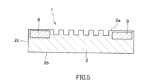
図1および図2は本発明の光インプリント用モールドの一実施形態を示す平面図であり、図3は図1のI−I矢視断面図である。図1〜図3において、光インプリント用モールド1は、透明な基材2と、この基材2の表面2a側に形成された凹凸パターン3aと、遮光部6とを有している。そして、図1および図3に示されるように、凹凸パターン3aが形成されたパターン領域3(図1では斜線を付して示す)の周囲に非パターン領域4が設けられている。また、図2および図3に示されるように、遮光部6は非パターン領域4の基材2の内部に存在しており、かつ、パターン領域3を含む所望の光透過領域5(図2において鎖線で囲まれた領域)を画定するように配設されている。
Hereinafter, embodiments of the present invention will be described with reference to the drawings.
[First Embodiment]
1 and 2 are plan views showing an embodiment of the optical imprint mold of the present invention, and FIG. 3 is a cross-sectional view taken along the arrow I-I in FIG. 1 to 3, the
上述の例では、遮光部6は基材2の厚みの略中央部に基材厚みの約半分の厚さで配設されているが、遮光部6の配設位置はこれに限定されるものではなく、遮光部6の光遮蔽性や画定する光透過領域5等を考慮して適宜設定することができる。例えば、図4に示されるように、基材2の厚みと略同等の厚さで配設されていてもよく、また、図5に示されるように、基材2の表面2a、裏面2bのいずれかの近傍(図5では表面2aの近傍)に配設されていてもよい。また、図6に示されるように、基材2の内部に埋設された遮光部6を被覆し、かつ、基材2の裏面2bと同一面をなすように保護平坦化層7が配設されていてもよい。
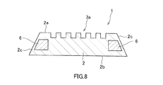
また、上述の例では、基材2の側面2cは主面である表面2a、裏面2cに対して垂直となる面であるが、本発明はこれに限定されるものではない。例えば、図7に示されるように、基材2の表面2a側に段差8を有する構造(メサ構造)、図8に示されるように、基材2の側面2cが傾斜している構造であってもよい。
In the above-described example, the
Moreover, in the above-mentioned example, although the
ここで、光透過領域5は、光インプリント用モールド1の裏面2b側から照射された光が被加工物を露光する領域である。この光透過領域5について、図9を参照しながら説明する。例えば、照射光に斜入射光成分が含まれ、その最大入射角がθである場合、光透過領域5は、この最大入射角θと、パターン領域3に最も近い遮光部6の端部6aの位置(特に、基材2の表面2aに最も近い端部6aの位置)と、基材2の表面2aから遮光部6までの深さdを適宜設定することにより画定できる。
Here, the
光インプリント用モールド1を構成する基材2は、被加工物を硬化させるための照射光を透過可能な透明基材である。このような基材2の材料としては、例えば、石英ガラス、珪酸系ガラス、フッ化カルシウム、フッ化マグネシウム、アクリルガラス、パイレックス(登録商標)ガラス、青板ガラス、ソーダガラス、BK−7等、あるいは、これらの任意の積層材を用いることができる。また、基材2の厚みは被加工物の材質、凹凸パターン3aの形状、基材の強度、取り扱い適性等を考慮して設定することができ、例えば、0.1〜10mm程度の範囲で適宜設定することができる。
光インプリント用モールド1を構成する凹凸パターン3aは、基材2の表面2aに形成されたマイクロ〜ナノオーダーの微細な凹凸構造である。図示例では、凹凸パターン3aは基材2にエッチングにより微細な凹部を形成して構成されている。また、基材2上に微細な凸部を配設して凹凸パターン3aとしてもよい。凹凸パターン3aの寸法、形状は用途等に応じて適宜設定することができ、特に限定されない。
The
The concavo-
光インプリント用モールド1を構成する遮光部6は、被加工物を硬化させるために光インプリント法で使用する照射光によって被加工物の意図しない部位が露光されるのを抑制するものであり、例えば、波長が200〜400nm程度の光に対する透過率が1%以下、好ましくは0.1%以下のものとすることができる。このような遮光部6は、基材2と同一の材料からなり、かつ、光学的性質が基材2と異なるものとすることができる。この場合、例えば、基材2の内部にレーザー光を収斂して基材2に絶縁破壊を生じさせクラック部位を形成し、これにより不透明な遮光部6とすることができる。また、基材2内部に結晶を析出させ結晶化部位を形成し、これにより不透明な遮光部6とすることができる。このような結晶化は、レーザー光の収斂等により行うことができる。
The
また、光インプリント用モールド1を構成する遮光部6は、基材2と異なる材料からなり、かつ、光学的性質が基材2と異なるものとすることができる。この場合、遮光部6は、例えば、基材2の内部に形成された気泡部位とすることができる。このような気泡部位からなる遮光部6は、予め基材2の製造工程において、気泡含有の石英ガラスと透明な石英ガラスをフッ酸接合する方法等により所定のパターンで形成することができる。また、気泡部位は、例えば、直径が10〜100μm程度の気泡が密集あるいは散在して構成されている層とすることができる。この気泡部位の気泡密度は、3×10⁵〜5×10⁶個/cm3の範囲で設定することができる。また、厚み方向の気泡密度、気泡直径が勾配を有するものであってもよい。尚、気泡の平均直径、気泡密度の測定は、目盛り付レンズをもつ偏光顕微鏡を用いて行うことができる。
Further, the light-shielding
また、図6に示したように、遮光部6は基材2の内部に埋設された遮光性材料からなり、この遮光性材料を被覆し、かつ、基材2の裏面2bと同一面をなすように保護平坦化層7を配設したものであってもよい。この場合、遮光性材料としては、アルミニウム、ニッケル、コバルト、クロム、チタン、タンタル、タングステン、モリブデン、錫、亜鉛等の金属、シリコン等を挙げることができ、また、これらの酸化物、窒化物、合金等も使用することができる。また、保護平坦化層7は、上記の基材2の材料として挙げた材料や、Spin on Glass等を用いて形成することができる。
このような光インプリント用モールド1は、所望の光透過領域5を画定するように遮光部6が配設されているので、被加工物の意図しない部位への露光が遮光部6によって確実に抑制され、また、遮光部6が基材の内部に存在し、基材2の表面や裏面に凸部となって存在していないので、モールド保持部で保持される部位に遮光部が存在しても、機械的外力による遮光部からの異物の発生が防止される。したがって、種々のインプリント装置のモールド保持機構に対応可能であり、インプリント装置の設計において、露光光学系の設計と、機械的な保持機構の設計を独立して行うことができ、装置設計の自由度が大幅に向上する。また、光インプリント用モールド1の裏面が平坦なので、吸着機構によりモールド保持を安定して行なうことができる。
Further, as shown in FIG. 6, the
Since such a
[第2の実施形態]
図10は本発明の光インプリント用モールドの他の実施形態を示す断面図であり、図1のI−I矢視における図3対応の断面図である。図10において、光インプリント用モールド11は、透明な基材12と、この基材12の表面12a側に形成された凹凸パターン13aと、遮光部16とを有している。この光インプリント用モールド11では、凹凸パターン13aが形成されたパターン領域13の周囲に非パターン領域14が設けられており、また、遮光部16は非パターン領域14に、基材12の裏面12bの表層から所定の深さまで存在して、かつ、パターン領域13を含む所望の光透過領域15を画定するように配設されている。このような光インプリント用モールド11におけるパターン領域13、非パターン領域14、光透過領域15は、上述の光インプリント用モールド1のパターン領域3、非パターン領域4、光透過領域5と同様であり、上述の図1および図2を参考とすることができる。
[Second Embodiment]
FIG. 10 is a cross-sectional view showing another embodiment of the optical imprint mold of the present invention, and is a cross-sectional view corresponding to FIG. In FIG. 10, the
上述の例では、遮光部16は基材12の裏面12bの表層から所定の深さまで存在しているが、遮光部16の配設位置はこれに限定されるものではなく、遮光部16の光遮蔽性や画定する光透過領域15等を考慮して適宜設定することができる。例えば、図11に示されるように、遮光部16が基材12の表面12aの表層から所定の深さまで存在していてもよい。また、例えば、図12に示されるように、基材12が表面12a側に段差18を有する構造(メサ構造)である場合に、段差18が形成された部位において、遮光部16が表層から所定の深さまで存在していてもよい。
In the above-described example, the
ここで、光透過領域15は、光インプリント用モールド1の裏面12b側から照射された光が被加工物を露光する領域である。この光透過領域15について、図13を参照しながら説明する。まず、図13(A)に示されるように、遮光部16が基材12の裏面12bの表層から所定の深さまで存在している場合、光透過領域15は、照射光の最大入射角θと、パターン領域13に最も近い遮光部16の端部16aの位置(特に、基材12の表面12aに最も近い端部16aの位置)と、基材12の表面12aから遮光部16までの深さdを適宜設定することにより画定できる。また、図13(B)に示されるように、遮光部16が基材12の表面12aの表層から所定の深さまで存在している場合、光透過領域15は、照射光の最大入射角θや遮光部16までの深さを考慮する必要はなく、パターン領域13に最も近い遮光部16の端部16aの位置を適宜設定することにより画定できる。
光インプリント用モールド11を構成する基材12、凹凸パターン13aは、上述の光インプリント用モールド1を構成する基材2、凹凸パターン3aと同様とすることができ、ここでの説明は省略する。
Here, the
The
光インプリント用モールド11を構成する遮光部16は、被加工物を硬化させるために光インプリント法で使用する照射光によって被加工物の意図しない部位が露光されるのを抑制するものであり、例えば、波長が200〜400nm程度の光に対する透過率が1%以下、好ましくは0.1%以下のものとすることができる。また、遮光部16の厚みは、その光遮蔽性を考慮して適宜設定することができる。
このような遮光部16は、例えば、基材12と同一の材料からなり、かつ、光学的性質が基材12と異なるものとすることができる。この場合、遮光部16は、基材12の光学的性質を変化させて形成した層とすることができ、例えば、結晶化部位を形成して遮光部16とすることができる。この結晶化部位は、上述の遮光部6において説明したように形成することができる。
The
Such a light-shielding
また、光インプリント用モールド11を構成する遮光部16は、基材12と異なる材料からなり、かつ、光学的性質が基材12と異なるものとすることができる。この場合、遮光部16は、基材12に添加された添加物により化学組成が変化してなる組成変化部位とすることができる。このような組成変化部位からなる遮光部16は、例えば、基材12にマンガン、銅、コバルト、クロム、鉄、ウラニウム、銀、ニッケル、カドミウム、セレン、金、ネオジム、フッ化カルシウム、フッ化ソーダ、リン酸カルシウム、硫黄等の添加物の1種または2種以上を添加して形成することができる。添加量は、用いる添加物、目標とする光隠蔽性等に応じて設定することができ、例えば、基材12の単位重量当りの添加量を0.2〜20g/kg程度の範囲で設定することができる。
さらに、基材12と異なる材料からなる遮光部16が、基材12に同一面となるように埋め込まれた遮光性材料からなるものであってもよい。遮光性材料としては、上述の遮光部6の説明で挙げた材料を使用することができる。
Further, the
Furthermore, the
このような本発明の光インプリント用モールド11は、所望の光透過領域15を画定するように遮光部16が配設されているので、被加工物の意図しない部位への露光が遮光部16によって確実に抑制される。また、遮光部16が基材12の表層から所定の深さまで存在し、基材12の表面や裏面に凸部となって存在していないので、モールド保持部で保持される部位に遮光部16が存在しても、機械的外力による遮光部16からの異物の発生が防止される。したがって、種々のインプリント装置のモールド保持機構に対応可能であり、インプリント装置の設計において、露光光学系の設計と、機械的な保持機構の設計を独立して行うことができ、装置設計の自由度が大幅に向上する。また、光インプリント用モールド11の裏面が平坦なので、吸着機構によるモールド保持が安定する。
Since the light-imprinting
次に、インプリント装置のモールド保持機構による本発明の光インプリント用モールドの保持の状態を図14〜図16を参照して説明する。
図14に示される例では、上述の図3に示されるような態様の本発明の光インプリント用モールド1の基材2の裏面2b側を吸着機構(真空チャック)21で吸着保持するものである。本発明では、遮光部が基材の裏面に凸部となって存在していないので、吸着機構によりモールド保持を安定して行なうことができる。
また、図15に示される例では、上述の図8に示されるような態様の本発明の光インプリント用モールド1の基材2の側面2cと裏面2bの周辺部を保持装置22で機械的に保持するものである。本発明では、遮光部が基材の裏面や側面に凸部となって存在していないので、保持装置22で保持される部位に遮光部が存在しても、機械的外力による遮光部からの異物の発生が防止される。
Next, the state of holding the optical imprint mold of the present invention by the mold holding mechanism of the imprint apparatus will be described with reference to FIGS.
In the example shown in FIG. 14, the
Further, in the example shown in FIG. 15, the holding
さらに、図16に示される例では、上述の図12に示されるような態様の本発明の光インプリント用モールド11の基材12の段差18が形成された部位を保持装置23で機械的に保持するものである。本発明では、遮光部16が基材12の表層から所定の深さまでに存在し、基材12の裏面12bや段差18が形成された面に凸部となって存在していないので、保持装置23で保持される部位に遮光部16が存在しても、機械的外力による遮光部からの異物の発生が防止される。
Further, in the example shown in FIG. 16, the portion where the
次いで、本発明の光インプリント用モールドを用いたインプリント装置による光インプリント法でのパターン形成の一例を図17および図18を参照して説明する。
図17に示されるように、本発明の光インプリント用モールド1が真空チャック21によって基材2の裏面2b側を吸着保持されている。そして、基板32の表面に光硬化性の樹脂層33を備えた被加工物31を基板ステージ28に載置し、樹脂層33に光インプリント用モールド1を圧着する。そして、この状態で照明光学系26から光インプリント用モールド1に紫外線を照射し、光インプリント用モールド1を透過した紫外線により樹脂層33を硬化させる。この際、光インプリント用モールド1を構成する遮光部6によって所定の光透過領域5(図2、図3、図9参照)が画定されているので、被加工物31の意図しない部位への露光が遮光部6によって確実に抑制される。尚、この紫外線照射において、照明光学系26からの紫外線を適切な部位に照射するためにブラインド27を照明光学系26と光インプリント用モールド1との間に介在させることに何ら制限はない。
その後、図18に示されるように、光インプリント用モールド1を樹脂層33から離型する。これにより、光インプリント用モールド1が有する凹凸パターン3aが反転した凹凸構造34が被加工物である樹脂層33に転写形成される。
上述の実施形態は例示であり、本発明はこれに限定されるものではない。
Next, an example of pattern formation by an optical imprint method using an imprint apparatus using the optical imprint mold of the present invention will be described with reference to FIGS.
As shown in FIG. 17, the
Thereafter, as shown in FIG. 18, the
The above-described embodiment is an exemplification, and the present invention is not limited to this.
次に、より具体的な実施例を示して本発明を更に詳細に説明する。
[参考例]
厚み675μmの石英ガラス(65mm角)を光インプリント用モールド用基材として準備した。この基材の表面にスパッタリング法によりクロム薄膜(厚み15nm)を成膜し、その後、このクロム薄膜上に市販のレジストを塗布した。
次いで、市販の電子線描画装置内のステージ上に、基材の裏面がステージと対向するように基材を配置し、レジストに電子線を照射して、所望のパターン潜像を形成した。
次に、レジストを現像してレジストパターンを形成し、このレジストパターンをマスクとしてドライエッチングにより基材に凹凸パターンを形成した。形成した凹凸パターンは深さ200nm、ライン/スペースが100nm/100nmであった。この凹凸パターンが形成されたパターン領域は、基材の中央に位置する35mm角の領域であった。
Next, the present invention will be described in more detail by showing more specific examples.
[ Reference example ]
Quartz glass (65 mm square) with a thickness of 675 μm was prepared as a substrate for molds for optical imprinting. A chromium thin film (
Next, the base material was placed on a stage in a commercially available electron beam drawing apparatus so that the back surface of the base material faces the stage, and the resist was irradiated with an electron beam to form a desired pattern latent image.
Next, the resist was developed to form a resist pattern, and an uneven pattern was formed on the substrate by dry etching using the resist pattern as a mask. The formed concavo-convex pattern had a depth of 200 nm and a line / space of 100 nm / 100 nm. The pattern area on which the uneven pattern was formed was a 35 mm square area located at the center of the substrate.
次に、この基材の表面(凹凸パターンを形成した面)側から、下記の条件でレーザー光を基材内部に収斂し絶縁破壊を生じさせてクラック部位からなる遮光部を深さ100〜500μmの位置に形成した。この遮光部の基材内側に向く端部(図9に示される端部6a)が囲む領域は35mm角であり、上記のパターン領域の外側を囲むものであった。また、基材の側面に向く遮光部の端部は、基材の側面から約100μm内側に位置するものであった。これにより、図3に示されるような光インプリント用モールドを作製した。
Next, from the surface (surface on which the concavo-convex pattern is formed) side of the base material, laser light is converged inside the base material under the following conditions to cause dielectric breakdown, and the light shielding portion consisting of the crack portion is 100 to 500 μm deep. Formed in the position. An area surrounded by an end portion (end
尚、このような遮光部の形成位置は、基材の中央に位置し、かつ、上記のパターン領域の外側を囲む35mm角の光透過領域(図2参照)を画定するものである。本実施例ではパターン領域と、遮光部が画定する光透過領域の大きさが同一となるよう作製することが可能であった。以下の実施例1〜4、比較例2〜3においても同様の光透過領域を画定するために遮光部を形成した。
(レーザー照射条件)
・使用レーザー : YAG
・照射エネルギー : 400μJ
上記のように遮光部を形成した部位と形成していない部位の光透過率を大塚電子(株)製 MCPDを用いて測定した結果、遮光部が形成された部位の光透過率は1%、形成されていない部位の光透過率は93%であった。
The formation position of such a light shielding part is located in the center of the substrate and defines a 35 mm square light transmission region (see FIG. 2) surrounding the outside of the pattern region. In this embodiment, it was possible to manufacture the pattern region and the light transmission region defined by the light shielding portion so as to have the same size. In Examples 1 to 4 and Comparative Examples 2 to 3 below, a light shielding portion was formed in order to define the same light transmission region.
(Laser irradiation conditions)
・ Laser used: YAG
・ Irradiation energy: 400μJ
As a result of measuring the light transmittance of the part where the light shielding part was formed as described above using the MCPD manufactured by Otsuka Electronics Co., Ltd., the light transmittance of the part where the light shielding part was formed was 1%, The light transmittance of the part which was not formed was 93%.
[実施例1]
まず、気泡含有の石英ガラス(65mm角)を作製した。すなわち、石英粉末(ユミニン(株)製 IOTA−5、平均粒子径300μm)100重量部に対して、窒化ケイ素粉末(宇部興産(株)製 SN−E10、平均粒子径0.5μm)を0.01重量部、エタノール50重量部を添加して攪拌、混合した。次いで、エタノールを除去し乾燥して得た混合粉末300gをカーボン製るつぼに充填(充填密度1.4g/cm3)し、電気炉内に入れ、雰囲気を1×10-3mmHgとした。その後、室温から1800℃まで300℃/時間の昇温速度で加熱し、1800℃に10分間保持した後、電気炉内が常圧に達するまで窒素ガスを導入した。これにより得られた気泡含有の石英ガラスの気泡の平均径は72μm、気泡密度は9×105個/cm3であった。
[Example 1 ]
First, bubble-containing quartz glass (65 mm square) was produced. In other words, 100 parts by weight of quartz powder (IOTA-5 manufactured by Yuminin Co., Ltd., average particle size: 300 μm) is 0.1% of silicon nitride powder (SN-E10 manufactured by Ube Industries, Ltd., average particle size: 0.5 μm). 01 parts by weight and 50 parts by weight of ethanol were added and stirred and mixed. Next, 300 g of mixed powder obtained by removing ethanol and drying was filled in a carbon crucible (filling density: 1.4 g / cm 3 ) and placed in an electric furnace to make the
次に、この石英ガラス(65mm角)の中心をフッ酸を用いて35mm角でくり抜いて、回廊形状の遮光部を作製した。その後、この遮光部のくり抜き箇所に石英ガラス(35mm角)をはめ込み、フッ酸接合で接合し、さらに、両面を機械研磨により平坦化して、厚み675μmの基材とした。
次いで、この基材の中央に位置する35mm角の領域(気泡を含有していない石英ガラス)に、参考例と同様にして、凹凸パターン(深さ200nm、ライン/スペース100nm/100nm)を作製した。これにより、図4に示されるような光インプリント用モールドを作製した。
上記のような遮光部(気泡含有の石英ガラス)と中央の石英ガラス(35mm角)の光透過率を参考例と同様に測定した結果、遮光部の光透過率は1%、中央の石英ガラスの光透過率は93%であった。
Next, the center of this quartz glass (65 mm square) was cut out with a 35 mm square using hydrofluoric acid to produce a corridor-shaped light shielding part. Thereafter, quartz glass (35 mm square) was fitted into the cut-out portion of the light shielding portion, joined by hydrofluoric acid joining, and further, both surfaces were flattened by mechanical polishing to obtain a substrate having a thickness of 675 μm.
Next, an uneven pattern (depth: 200 nm, line / space: 100 nm / 100 nm) was produced in a 35 mm square region (quartz glass containing no bubbles) located in the center of the substrate in the same manner as in the reference example . . Thereby, a mold for optical imprinting as shown in FIG. 4 was produced.
As a result of measuring the light transmittance of the light shielding part (bubble-containing quartz glass) and the central quartz glass (35 mm square) in the same manner as in the reference example , the light transmittance of the light shielding part was 1%, and the central quartz glass. The light transmittance of was 93%.
[実施例2]
参考例と同様にして、基材の表面に凹凸パターンの形成までを行った。
次いで、この基材の裏面(凹凸パターンが形成されていない面)に市販のレジストを塗布し、所定のフォトマスクを介して露光し現像することにより、表面の凹凸パターンが中央に位置するように裏面に35mm角のレジストパターンを形成し、また、基材裏面の周辺部に幅が4mmのレジストパターンを形成した。このレジストパターンをマスクとしてドライエッチングにより基材の裏面をエッチングして深さ1μmの凹部を形成した。次いで、スパッタリング法により、上記の凹部内にクロム薄膜(厚み100nm)を形成し、上記のレジストパターンを剥離した。その後、このクロム薄膜を被覆するように溶融状態のSpin on Glassを配設し、硬化後に機械研磨によって基材裏面を平坦なものとした。これにより、基材内部にクロム薄膜(遮光性材料)が埋設されてなる遮光部を形成した(図6参照)。この遮光部の基材内側に向く端部(図9に示される端部6a)が囲む領域は35mm角であり、上記のパターン領域の外側を囲むものであった。また、基材の側面に向く遮光部の端部は、基材の側面から約4mm内側に位置するものであった。これにより、図6に示されるような光インプリント用モールドを作製した。
[Example 2 ]
In the same manner as in the reference example , the formation of the uneven pattern on the surface of the substrate was performed.
Next, a commercially available resist is applied to the back surface (the surface on which the uneven pattern is not formed) of this base material, and exposure and development are performed through a predetermined photomask so that the uneven pattern on the front surface is positioned at the center. A 35 mm square resist pattern was formed on the back surface, and a resist pattern with a width of 4 mm was formed on the periphery of the back surface of the substrate. Using this resist pattern as a mask, the back surface of the substrate was etched by dry etching to form a recess having a depth of 1 μm. Next, a chromium thin film (thickness: 100 nm) was formed in the recess by sputtering, and the resist pattern was peeled off. Thereafter, spin-on-glass in a molten state was disposed so as to cover the chromium thin film, and the substrate back surface was flattened by mechanical polishing after curing. This formed the light-shielding part by which the chromium thin film (light-shielding material) was embed | buried under the base material (refer FIG. 6). An area surrounded by an end portion (end
上記のように遮光部を形成した部位と形成していない部位の光透過率を参考例と同様に測定した結果、遮光部が形成された部位の光透過率は0.1%、形成されていない部位の光透過率は93%であった。 As described above, the light transmittance of the portion where the light shielding portion is formed and the portion where the light shielding portion is not formed are measured in the same manner as in the reference example . As a result, the light transmittance of the portion where the light shielding portion is formed is 0.1%. The light transmittance of the part which is not present was 93%.
[実施例3]
まず、銅赤色ガラス(65mm角)を作製した。すなわち、ベースガラス(含有鉄分量はFe2O3換算で0.015重量%)を溶融窯で溶融し、これに接続するカララントフォアハース内で、酸化第二銅(CuO)13.965重量%、酸化第一スズ(SnO)5.98重量%、炭素0.05重量%を含むフリットを1.0重量%添加し、さらに、金属セレン(Se)1.344重量%を含むフリットを0.15重量%添加し均一に混合し、成形後、最高温度600℃において、60分間徐冷(熱処理)を行い、銅赤色ガラスとした。
次に、この銅赤色ガラス(65mm角)の中心をフッ酸を用いて35mm角でくり抜いて、回廊形状の遮光部を作製した。その後、この遮光部のくり抜き箇所に石英ガラス(35mm角)をはめ込み、フッ酸接合で接合し、さらに、両面を機械研磨により平坦化して、厚み675μmの基材とした。
次いで、この基材の中央に位置する35mm角の領域(石英ガラス)に、参考例と同様にして、凹凸パターン(深さ200nm、ライン/スペース100nm/100nm)を作製した。これにより、図4に示されるような光インプリント用モールドを作製した。
上記のような遮光部(銅赤色ガラス)と中央の石英ガラス(35mm角)の光透過率を参考例と同様に測定した結果、遮光部の光透過率は1%、中央の石英ガラスの光透過率は93%であった。
[Example 3 ]
First, copper red glass (65 mm square) was produced. That is, base glass (the iron content is 0.015 wt% in terms of Fe 2 O 3 ) is melted in a melting kiln, and cuprous oxide (CuO) 13.965 wt. %, A frit containing stannous oxide (SnO) 5.98% by weight and carbon 0.05% by weight is added, and a frit containing 1.344% by weight of metal selenium (Se) is further added. .15% by weight was added and mixed uniformly, and after molding, it was gradually cooled (heat treatment) at a maximum temperature of 600 ° C. for 60 minutes to obtain a copper red glass.
Next, the center of this copper red glass (65 mm square) was hollowed out with a 35 mm square using hydrofluoric acid to produce a corridor-shaped light shielding part. Thereafter, quartz glass (35 mm square) was fitted into the cut-out portion of the light shielding portion, joined by hydrofluoric acid joining, and further, both surfaces were flattened by mechanical polishing to obtain a substrate having a thickness of 675 μm.
Next, an uneven pattern (depth 200 nm, line / space 100 nm / 100 nm) was produced in a 35 mm square region (quartz glass) located at the center of the substrate in the same manner as in the reference example . Thereby, a mold for optical imprinting as shown in FIG. 4 was produced.
The light transmittance of the light shielding part (copper red glass) and the central quartz glass (35 mm square) as described above was measured in the same manner as in the reference example . As a result, the light transmittance of the light shielding part was 1% and the light of the central quartz glass. The transmittance was 93%.
[実施例4]
参考例と同様にして、基材の表面に凹凸パターンの形成までを行った。
次いで、この基材の裏面(凹凸パターンが形成されていない面)に実施例2で使用したのと同じ市販のレジストを塗布し、所定のフォトマスクを介して露光し現像することにより、表面の凹凸パターンが中央に位置するように裏面に35mm角のレジストパターンを形成した。このレジストパターンをマスクとしてドライエッチングにより基材の裏面をエッチングして深さ100nmの凹部を形成した。次いで、スパッタリング法により、上記の凹部内にクロム薄膜(厚み100nm)を形成し、上記のレジストパターンを剥離した。その後、機械研磨によって基材裏面を平坦なものとした。これにより、基材裏面の表層から深さ100nmまでクロム薄膜(遮光性材料)が埋め込まれてなる遮光部を形成した(図10参照)。この遮光部の基材内側に向く端部(図9に示される端部6a)が囲む領域は35mm角であり、上記のパターン領域の外側を囲むものであった。これにより、図10に示されるような光インプリント用モールドを作製した。
上記のように遮光部を形成した部位と形成していない部位の光透過率を参考例と同様に測定した結果、遮光部が形成された部位の光透過率は0.1%、形成されていない部位の光透過率は93%であった。
[Example 4 ]
In the same manner as in the reference example , the formation of the uneven pattern on the surface of the substrate was performed.
Next, the same commercially available resist as used in Example 2 was applied to the back surface (the surface on which the concave / convex pattern was not formed) of this base material, and exposed and developed through a predetermined photomask, thereby A 35 mm square resist pattern was formed on the back surface so that the concavo-convex pattern was located in the center. Using this resist pattern as a mask, the back surface of the substrate was etched by dry etching to form a recess having a depth of 100 nm. Next, a chromium thin film (thickness: 100 nm) was formed in the recess by sputtering, and the resist pattern was peeled off. Thereafter, the back surface of the substrate was made flat by mechanical polishing. This formed the light shielding part in which the chromium thin film (light shielding material) was embedded from the surface layer on the back surface of the base material to a depth of 100 nm (see FIG. 10 ). An area surrounded by an end portion (end
As described above, the light transmittance of the portion where the light shielding portion is formed and the portion where the light shielding portion is not formed are measured in the same manner as in the reference example . As a result, the light transmittance of the portion where the light shielding portion is formed is 0.1%. The light transmittance of the non-existing part was 93%.
[比較例1]
遮光部を形成しない他は、参考例と同様にして、光インプリント用モールドを作製した。
[Comparative Example 1]
An optical imprint mold was produced in the same manner as in the reference example except that the light shielding portion was not formed.
[比較例2]
参考例と同様にして、基材の表面に凹凸パターンの形成までを行った。
次いで、この基材の裏面(凹凸パターンが形成されていない面)に実施例3で使用したのと同じ市販のレジストを塗布し、所定のフォトマスクを介して露光し現像することにより、表面の凹凸パターンが中央に位置するように裏面に35mm角のレジストパターンを形成した。このレジストパターンをマスクとしてスパッタリング法により、基板裏面にクロム薄膜(厚み100nm)を形成し、上記のレジストパターンを剥離した。これにより、基材裏面にクロム薄膜からなる遮光部を形成した。この遮光部の基材内側に向く端部(図9に示される端部6a)が囲む領域は35mm角であり、上記のパターン領域の外側を囲むものであった。これにより、光インプリント用モールドを作製した。
上記のように遮光部を形成した部位と形成していない部位の光透過率を参考例と同様に測定した結果、遮光部が形成された部位の光透過率は0.1%、形成されていない部位の光透過率は93%であった。
[Comparative Example 2]
In the same manner as in the reference example , the formation of the uneven pattern on the surface of the substrate was performed.
Next, the same commercially available resist as used in Example 3 was applied to the back surface (the surface on which the concave / convex pattern was not formed) of the base material, and exposed and developed through a predetermined photomask, thereby A 35 mm square resist pattern was formed on the back surface so that the concavo-convex pattern was located in the center. Using this resist pattern as a mask, a chromium thin film (thickness: 100 nm) was formed on the back surface of the substrate by sputtering, and the resist pattern was peeled off. This formed the light-shielding part which consists of a chromium thin film in the base-material back surface. An area surrounded by an end portion (end
As described above, the light transmittance of the portion where the light shielding portion is formed and the portion where the light shielding portion is not formed are measured in the same manner as in the reference example . As a result, the light transmittance of the portion where the light shielding portion is formed is 0.1%. The light transmittance of the non-existing part was 93%.
[評価1]
上述のように作製した光インプリント用モールド(参考例、実施例1〜4、比較例1〜2)について、下記の各評価を行った。
<吸着保持の安定性>
外形が65mm角である各光インプリント用モールドの裏面を、下記の真空チャック1を用いて保持し、インプリント装置を使用してパターン転写を実施した。すなわち、6インチ径のシリコンウエハ基板の表面に厚み0.7μmの光硬化性樹脂層(東洋合成工業(株)製 PAK−01)を備えた被加工物を、インプリント装置の基板ステージに載置した。次いで、光硬化性樹脂層に光インプリント用モールドを押し当てた(光硬化性樹脂層への押し込み量=0.1μm)。この状態で光インプリント装置の照明光学系から紫外線(ピーク波長365nm)を照射し、光インプリント用モールドを透過した紫外線により光硬化性樹脂層を硬化させた。その後、光インプリント用モールドを被加工物から離型する。このようなパターン転写を10回実施し、吸着保持の安定性を下記の基準で判定して表1に示した。
[Evaluation 1]
The following evaluation was performed about the mold for optical imprint produced as mentioned above ( reference example, Examples 1-4 , Comparative Examples 1-2).
<Stability of adsorption retention>
The back surface of each optical imprint mold having an outer shape of 65 mm square was held using the
(真空チャック1)
光インプリント用モールドを、周囲から15mmの範囲で吸着保持するもので
あり、モールドと真空チャック1との接触領域における吸着部の分布は均一で
あり、かつ、モールドと真空チャック1との接触面積当りの吸着部の面積比率
は0.4である。したがって、真空チャック1の中心を光が通過してモールド
に対して光照射が可能な領域の大きさは35mm角である。
(吸着保持安定性の判定基準)
○ : 被加工物からの離型時に、モールドが真空チャック1に保持され
ている
× : 被加工物からの離型時に、被加工物側にモールドが貼り付くこと
がある
(Vacuum chuck 1)
The optical imprint mold is sucked and held within a range of 15 mm from the periphery, the distribution of the sucking portion in the contact area between the mold and the
(Criteria for adsorption retention stability)
○: The mold is held by the
ing
×: The mold is attached to the workpiece side when releasing from the workpiece.
Is
<不要露光防止効果>
光インプリント用モールドを上記の真空チャック1により保持してインプリント装置に装着した。また、6インチ径のシリコンウエハ基板の表面に厚み0.7μmの光硬化性樹脂層(東洋合成工業(株)製 PAK−01)を備えた被加工物を、インプリント装置の基板ステージに載置した。
次いで、光硬化性樹脂層に光インプリント用モールドを圧着(光硬化性樹脂層への押し込み量=0.1μm)した。この状態でインプリント装置の照明光学系から紫外線(ピーク波長=365nm)を照射し、光インプリント用モールドを透過した紫外線により光硬化性樹脂層を硬化させた。その後、光インプリント用モールドを被加工物から離型し、光インプリント用モールドが有する凹凸パターンの反転凹凸構造が転写形成された樹脂層を得た。
<Anti-exposure prevention effect>
The optical imprint mold was held by the
Next, a mold for photoimprinting was pressure-bonded to the photocurable resin layer (the amount of pressing into the photocurable resin layer = 0.1 μm). In this state, ultraviolet light (peak wavelength = 365 nm) was irradiated from the illumination optical system of the imprint apparatus, and the photocurable resin layer was cured by the ultraviolet light transmitted through the mold for photoimprint. Then, the mold for optical imprint was released from the workpiece, and a resin layer was obtained in which the inverted concavo-convex structure of the concavo-convex pattern of the optical imprint mold was transferred.
次いで、この樹脂層の未硬化部位をアセトンによって除去し、基板上に残存する樹脂層(反転凹凸構造が転写形成されている)を光硬化領域として測定した。この光硬化領域と、上述の光透過領域(35mm角)とを比較し、遮光部による不要露光防止効果を下記の基準で判定して表1に示した。
(不要露光防止効果の判定基準)
○ : 光硬化領域と光透過領域が一致している
△ : 光硬化領域が光透過領域よりも広く、その差は50μm未満
× : 光硬化領域が光透過領域よりも広く、その差は50μm以上
Next, the uncured portion of the resin layer was removed with acetone, and the resin layer remaining on the substrate (in which the inverted concavo-convex structure was transferred) was measured as a photocured region. This photocured region was compared with the above-described light transmissive region (35 mm square), and the effect of preventing unnecessary exposure by the light-shielding portion was determined according to the following criteria and shown in Table 1.
(Criteria for unnecessary exposure prevention effect)
○: The photocuring region and the light transmission region match
Δ: The photocuring region is wider than the light transmitting region, and the difference is less than 50 μm.
×: The photocuring region is wider than the light transmission region, and the difference is 50 μm or more.
<異物発生の有無>
各光インプリント用モールドを真空チャック1で保持し、着脱を50回繰り返した。この着脱の繰り返しは、6インチ径のシリコンウエハを下方に配して行い、50回の着脱が終了した後、6インチ径のシリコンウエハ上の異物を異物検査機((株)トプコン製 WM−7)で検査し、下記の基準で異物発生の有無を判定して表1に示した。
(異物発生有無の判定基準)
無 : 1.0μmの異物の増加数が10個/cm2以下である
有 : 1.0μmの異物の増加数が10個/cm2を超える
<Existence of foreign matter>
Each mold for optical imprinting was held by the
(Judgment criteria for foreign matter occurrence)
None: Increase in the number of foreign matters of 1.0 μm is 10 / cm 2 or less.
Existence: Increase in the number of foreign particles of 1.0 μm exceeds 10 / cm 2
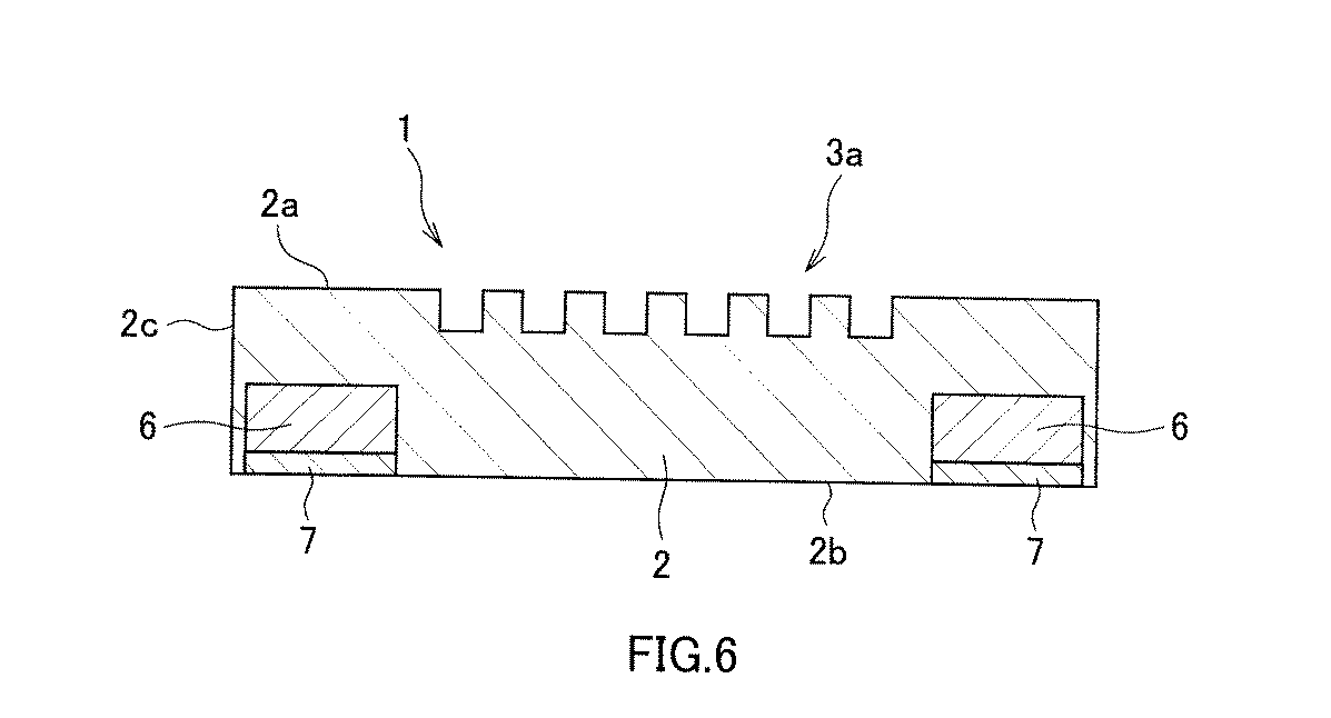
表1に示されるように、吸着保持安定性を見ると、ここで使用した真空チャック1は、全てのモールドを安定して保持することが可能であることがわかる。
また、不要露光防止効果を見ると、比較例1では不要部が露光されることが明らかである。比較例1は、遮光部を具備していないので、真空チャック1が実質的に遮光部となる役割を果たしている。しかし、真空チャック1では、光透過領域(35mm角)以外の部位を遮光することができないため、不要部が露光されてしまっている。一般に、真空チャックの寸法精度、モールドとのアライメント精度の制約を考えると、光透過領域以外の部位を真空チャックで完全に保持することは事実上不可能であり、不要露光防止効果の面で、比較例1は実施例1〜4および比較例2に対して大きく劣るものとなっている。
As shown in Table 1, it can be seen from the suction holding stability that the
Moreover, when the unnecessary exposure prevention effect is seen, in Comparative Example 1, it is clear that an unnecessary part is exposed. Since the comparative example 1 is not provided with the light shielding part, the
さらに、異物発生を見ると、比較例2において異物発生が確認された。これは、比較例2では、基材裏面に厚み100nmで形成したクロム薄膜からなる遮光部が真空チャック1と繰り返し接触することで、遮光部を構成するクロム薄膜が剥がれたものである。したがって、遮光部が基材内部に存在するか、基材と同一面となるように埋め込まれているモールド(実施例1〜4)は、従来のモールドである比較例2に比して優れていることが明らかである。
このような評価1の比較例2の結果から、基材裏面に突出するように設けられた遮光部に直接真空チャックが接触することが異物発生の原因であることが理解できた。そこで、真空チャックにより保持するための部位には遮光部を存在させないように比較例2を改善した下記の比較例3のモールドを作製した。
Furthermore, when the occurrence of foreign matter was observed, the occurrence of foreign matter was confirmed in Comparative Example 2. In Comparative Example 2, the light shielding part made of a chromium thin film formed with a thickness of 100 nm on the back surface of the base material is repeatedly brought into contact with the
From the result of Comparative Example 2 of
[比較例3]
実施例1と同様にして、基材の表面に凹凸パターンの形成までを行った。
次いで、この基材の裏面(凹凸パターンが形成されていない面)に実施例2で使用したのと同じ市販のレジストを塗布し、所定のフォトマスクを介して露光し現像することにより、表面の凹凸パターンが中央に位置するように裏面に35mm角のレジストパターンを形成し、また、基材裏面の周辺部に幅が10mmのレジストパターンを形成した。た。このレジストパターンをマスクとしてスパッタリング法により、基板裏面にクロム薄膜(厚み100nm)を形成し、上記のレジストパターンを剥離した。これにより、基材裏面にクロム薄膜からなる遮光部を形成した。この遮光部の基材内側に向く端部(図9に示される端部6a)が囲む領域は35mm角であり、上記のパターン領域の外側を囲むものであった。また、基材の側面に向く遮光部の端部は、基材の側面から約10mm内側に位置するものであった。これにより、光インプリント用モールドを作製した。
上記のように遮光部を形成した部位と形成していない部位の光透過率を参考例と同様に測定した結果、遮光部が形成された部位の光透過率は0.1%、形成されていない部位の光透過率は93%であった。
上記のように遮光部を形成した部位と形成していない部位の光透過率を参考例と同様に測定した結果、遮光部が形成された部位の光透過率は0.1%、形成されていない部位の光透過率は93%であった。
[Comparative Example 3]
In the same manner as in Example 1 , the formation of the uneven pattern on the surface of the substrate was performed.
Next, the same commercially available resist as used in Example 2 was applied to the back surface (the surface on which the concave / convex pattern was not formed) of this base material, and exposed and developed through a predetermined photomask, thereby A 35 mm square resist pattern was formed on the back surface so that the concavo-convex pattern was located at the center, and a resist pattern having a width of 10 mm was formed on the peripheral portion of the back surface of the substrate. It was. Using this resist pattern as a mask, a chromium thin film (thickness: 100 nm) was formed on the back surface of the substrate by sputtering, and the resist pattern was peeled off. This formed the light-shielding part which consists of a chromium thin film in the base-material back surface. An area surrounded by an end portion (end
As described above, the light transmittance of the portion where the light shielding portion is formed and the portion where the light shielding portion is not formed are measured in the same manner as in the reference example . As a result, the light transmittance of the portion where the light shielding portion is formed is 0.1%. The light transmittance of the part which is not present was 93%.
As described above, the light transmittance of the portion where the light shielding portion is formed and the portion where the light shielding portion is not formed are measured in the same manner as in the reference example . As a result, the light transmittance of the portion where the light shielding portion is formed is 0.1%. The light transmittance of the non-existing part was 93%.
[評価2]
上述のように作製した比較例3の光インプリント用モールドと、上記の実施例1〜4の光インプリントモールドについて、下記の真空チャック2を用いて、評価1と同様にして、吸着保持の安定性と異物発生の有無を判定して表2に示した。
(真空チャック2)
光インプリント用モールドを、周囲から5mmの範囲で吸着保持するものであ
り、モールドと真空チャック2との接触領域における吸着部の分布は均一であ
り、かつ、モールドと真空チャック2との接触面積当りの吸着部の面積比率は
0.4である。したがって、真空チャック2の中心を光が通過してモールドに
対して光照射が可能な領域の大きさは55mm角である。
[Evaluation 2]
About the optical imprint mold of Comparative Example 3 produced as described above and the optical imprint molds of Examples 1 to 4 above, the following
(Vacuum chuck 2)
The optical imprint mold is sucked and held within a range of 5 mm from the surroundings. The distribution of the suction part in the contact area between the mold and the
表2に示されるように、比較例3では、基材裏面に厚み100nmで形成したクロム薄膜からなる遮光部が、基材の側面から内側の約10mmの幅の部位には存在せず、真空チャック2は、このように遮光部が存在しないモールドの周辺部位を保持するので、異物の発生はみられなかった。
しかし、真空チャック2は真空チャック1に比べて保持部分の面積が十分ではなかったため、全てのモールド(実施例1〜4、比較例3)に対し、良好な吸着保持安定性を発現できないものであった。
以上の評価1、評価2の結果から、ナノインプリント装置が、例えば、モールドの裏面側を吸着保持することを必要とした場合、本発明のモールドでは異物を発生させず、不要部の露光が行われない状態であって、かつ吸着保持安定性を得ることが可能であるが、従来のモールドでは不可能であることが確認された。
As shown in Table 2, in Comparative Example 3, the light-shielding portion formed of a chromium thin film formed on the back surface of the base material with a thickness of 100 nm does not exist in a portion having a width of about 10 mm inside from the side surface of the base material. Since the
However, since the area of the holding part of the
From the results of the
ナノインプリント技術を用いた微細加工に利用可能である。 It can be used for microfabrication using nanoimprint technology.
1,11…光インプリント用モールド
2,12…基材
3a,13a…凹凸パターン
3,13…パターン領域
4,14…非パターン領域
5,15…光透過領域
6,16…遮光部
7…保護平坦化層
DESCRIPTION OF
Claims (3)
Priority Applications (1)
| Application Number | Priority Date | Filing Date | Title |
|---|---|---|---|
| JP2009095556A JP5381259B2 (en) | 2009-04-10 | 2009-04-10 | Optical imprint mold |
Applications Claiming Priority (1)
| Application Number | Priority Date | Filing Date | Title |
|---|---|---|---|
| JP2009095556A JP5381259B2 (en) | 2009-04-10 | 2009-04-10 | Optical imprint mold |
Related Child Applications (1)
| Application Number | Title | Priority Date | Filing Date |
|---|---|---|---|
| JP2013157341A Division JP5821909B2 (en) | 2013-07-30 | 2013-07-30 | Optical imprint mold and manufacturing method thereof |
Publications (2)
| Publication Number | Publication Date |
|---|---|
| JP2010245470A JP2010245470A (en) | 2010-10-28 |
| JP5381259B2 true JP5381259B2 (en) | 2014-01-08 |
Family
ID=43098117
Family Applications (1)
| Application Number | Title | Priority Date | Filing Date |
|---|---|---|---|
| JP2009095556A Expired - Fee Related JP5381259B2 (en) | 2009-04-10 | 2009-04-10 | Optical imprint mold |
Country Status (1)
| Country | Link |
|---|---|
| JP (1) | JP5381259B2 (en) |
Families Citing this family (6)
| Publication number | Priority date | Publication date | Assignee | Title |
|---|---|---|---|---|
| FR2955522B1 (en) * | 2010-01-28 | 2012-02-24 | Commissariat Energie Atomique | MOLD FOR UV ASSISTED NANO-PRINTING LITHOGRAPHY AND METHODS OF MAKING SUCH A MOLD |
| JP2012253303A (en) * | 2011-06-07 | 2012-12-20 | Hitachi High-Technologies Corp | Micro structure transfer stamper and micro structure transfer device mounted with the same |
| JP5537517B2 (en) * | 2011-09-09 | 2014-07-02 | 株式会社東芝 | Template cleaning device |
| JP6409284B2 (en) * | 2014-02-25 | 2018-10-24 | 大日本印刷株式会社 | Imprint mold substrate, imprint mold, method for producing the same, and method for regenerating imprint mold |
| JP6569189B2 (en) * | 2014-04-01 | 2019-09-04 | 大日本印刷株式会社 | Imprint mold substrate and method for producing the same, imprint method, imprint mold and method for regenerating the same |
| US11040482B2 (en) * | 2017-02-28 | 2021-06-22 | Toshiba Kikai Kabushiki Kaisha | Transfer method, transfer apparatus, and mold |
Family Cites Families (3)
| Publication number | Priority date | Publication date | Assignee | Title |
|---|---|---|---|---|
| JPH02289311A (en) * | 1989-01-25 | 1990-11-29 | Hoya Corp | Manufacture of stamper and board for information recording medium for which stamper is used |
| JP4303846B2 (en) * | 1999-10-04 | 2009-07-29 | 大日本印刷株式会社 | Card issuance processing method |
| US6653030B2 (en) * | 2002-01-23 | 2003-11-25 | Hewlett-Packard Development Company, L.P. | Optical-mechanical feature fabrication during manufacture of semiconductors and other micro-devices and nano-devices that include micron and sub-micron features |
-
2009
- 2009-04-10 JP JP2009095556A patent/JP5381259B2/en not_active Expired - Fee Related
Also Published As
| Publication number | Publication date |
|---|---|
| JP2010245470A (en) | 2010-10-28 |
Similar Documents
| Publication | Publication Date | Title |
|---|---|---|
| JP5821909B2 (en) | Optical imprint mold and manufacturing method thereof | |
| JP5381259B2 (en) | Optical imprint mold | |
| JP5257225B2 (en) | Nanoimprint mold and manufacturing method thereof | |
| CN101154035B (en) | Fine mold and method for regenerating fine mold | |
| JP4869263B2 (en) | mold | |
| US11340526B2 (en) | Production method of template, template blank, and template substrate for imprinting, production method of template for imprinting, and template | |
| JP6111783B2 (en) | Imprint method and imprint apparatus | |
| JP6019685B2 (en) | Nanoimprint method and nanoimprint apparatus | |
| JP2008230232A (en) | Mold, manufacturing method of mold, imprint device and imprint method, and manufacturing method of structure using imprint method | |
| JP2008221674A (en) | Mold, manufacturing method of mold, processing apparatus, and processing method | |
| KR101663842B1 (en) | Substrate with multilayer reflection film, reflective mask blank and method for manufacturing reflective mask blank | |
| JP2011114046A (en) | Pattern forming method, pattern forming apparatus, nano-imprint mold, and method of manufacturing nano-imprint mold | |
| KR20110093654A (en) | Pattern forming method | |
| JP2010287625A (en) | Template and pattern forming method | |
| JP6669432B2 (en) | Alignment method, imprint method, and imprint apparatus | |
| JP5773024B2 (en) | Nanoimprint pattern forming equipment | |
| JP5050532B2 (en) | Imprint mold, imprint mold manufacturing method, and surface modification apparatus | |
| JP5407525B2 (en) | Nanoimprint transfer substrate and nanoimprint transfer method | |
| JP2015138928A (en) | Manufacturing method of mold for imprinting | |
| JP2007210275A (en) | Mold for imprint | |
| JP2018022807A (en) | Alignment method, imprint method, and imprint device | |
| JP2013239620A (en) | Pattern forming method | |
| TW200412471A (en) | Mask having a pellicle and manufacturing method thereof | |
| JP2011146496A (en) | Mold for optical imprint, and optical imprint method using the same | |
| JP4852225B2 (en) | Exposure apparatus and exposure method |
Legal Events
| Date | Code | Title | Description |
|---|---|---|---|
| A621 | Written request for application examination |
Free format text: JAPANESE INTERMEDIATE CODE: A621 Effective date: 20120216 |
|
| A977 | Report on retrieval |
Free format text: JAPANESE INTERMEDIATE CODE: A971007 Effective date: 20130315 |
|
| A131 | Notification of reasons for refusal |
Free format text: JAPANESE INTERMEDIATE CODE: A131 Effective date: 20130326 |
|
| A521 | Written amendment |
Free format text: JAPANESE INTERMEDIATE CODE: A523 Effective date: 20130516 |
|
| A131 | Notification of reasons for refusal |
Free format text: JAPANESE INTERMEDIATE CODE: A131 Effective date: 20130611 |
|
| A521 | Written amendment |
Free format text: JAPANESE INTERMEDIATE CODE: A523 Effective date: 20130717 |
|
| TRDD | Decision of grant or rejection written | ||
| A01 | Written decision to grant a patent or to grant a registration (utility model) |
Free format text: JAPANESE INTERMEDIATE CODE: A01 Effective date: 20130903 |
|
| A61 | First payment of annual fees (during grant procedure) |
Free format text: JAPANESE INTERMEDIATE CODE: A61 Effective date: 20130916 |
|
| R150 | Certificate of patent or registration of utility model |
Ref document number: 5381259 Country of ref document: JP Free format text: JAPANESE INTERMEDIATE CODE: R150 Free format text: JAPANESE INTERMEDIATE CODE: R150 |
|
| LAPS | Cancellation because of no payment of annual fees |