JP5375375B2 - Semiconductor integrated circuit and liquid crystal driving circuit - Google Patents
Semiconductor integrated circuit and liquid crystal driving circuit Download PDFInfo
- Publication number
- JP5375375B2 JP5375375B2 JP2009158067A JP2009158067A JP5375375B2 JP 5375375 B2 JP5375375 B2 JP 5375375B2 JP 2009158067 A JP2009158067 A JP 2009158067A JP 2009158067 A JP2009158067 A JP 2009158067A JP 5375375 B2 JP5375375 B2 JP 5375375B2
- Authority
- JP
- Japan
- Prior art keywords
- channel
- converter
- switch
- signal
- order
- Prior art date
- Legal status (The legal status is an assumption and is not a legal conclusion. Google has not performed a legal analysis and makes no representation as to the accuracy of the status listed.)
- Expired - Fee Related
Links
Images


Classifications
-
- G—PHYSICS
- G09—EDUCATION; CRYPTOGRAPHY; DISPLAY; ADVERTISING; SEALS
- G09G—ARRANGEMENTS OR CIRCUITS FOR CONTROL OF INDICATING DEVICES USING STATIC MEANS TO PRESENT VARIABLE INFORMATION
- G09G3/00—Control arrangements or circuits, of interest only in connection with visual indicators other than cathode-ray tubes
- G09G3/20—Control arrangements or circuits, of interest only in connection with visual indicators other than cathode-ray tubes for presentation of an assembly of a number of characters, e.g. a page, by composing the assembly by combination of individual elements arranged in a matrix no fixed position being assigned to or needed to be assigned to the individual characters or partial characters
- G09G3/34—Control arrangements or circuits, of interest only in connection with visual indicators other than cathode-ray tubes for presentation of an assembly of a number of characters, e.g. a page, by composing the assembly by combination of individual elements arranged in a matrix no fixed position being assigned to or needed to be assigned to the individual characters or partial characters by control of light from an independent source
- G09G3/36—Control arrangements or circuits, of interest only in connection with visual indicators other than cathode-ray tubes for presentation of an assembly of a number of characters, e.g. a page, by composing the assembly by combination of individual elements arranged in a matrix no fixed position being assigned to or needed to be assigned to the individual characters or partial characters by control of light from an independent source using liquid crystals
- G09G3/3611—Control of matrices with row and column drivers
- G09G3/3685—Details of drivers for data electrodes
- G09G3/3688—Details of drivers for data electrodes suitable for active matrices only
-
- G—PHYSICS
- G09—EDUCATION; CRYPTOGRAPHY; DISPLAY; ADVERTISING; SEALS
- G09G—ARRANGEMENTS OR CIRCUITS FOR CONTROL OF INDICATING DEVICES USING STATIC MEANS TO PRESENT VARIABLE INFORMATION
- G09G2310/00—Command of the display device
- G09G2310/02—Addressing, scanning or driving the display screen or processing steps related thereto
- G09G2310/0264—Details of driving circuits
- G09G2310/027—Details of drivers for data electrodes, the drivers handling digital grey scale data, e.g. use of D/A converters
Abstract
Description
本発明は、冗長回路を備える複数のDA変換器が組み込まれた半導体集積回路又は液晶駆動回路に関する。 The present invention relates to a semiconductor integrated circuit or a liquid crystal driving circuit in which a plurality of DA converters including redundant circuits are incorporated.
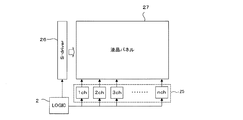
半導体基板上に多数のDA変換器を並列に形成した半導体集積回路が多方面に利用されている。例えば液晶表示装置用の液晶パネルでは、多数の走査線と多数の信号線の交差部に画素が構成され、走査線と信号線に走査信号と映像信号を与えて各画素を駆動する(例えば特許文献1を参照)。図14は、液晶パネルに映像信号を供給する信号ドライバのDA変換器100を表す模式図である。ロジック回路120は、映像表示用のシリアルデータを直列接続するラインバッファ131〜139に供給する。ラインバッファ131〜139は、入力したシリアルデータを各チャンネル用のパラレルデータに変換する。各DA変換器141〜149は、各チャンネルのデジタルデータをアナログデータに変換し、各増幅器151〜159へ出力する。各増幅器151〜159は、DA変換器141〜149から入力したアナログデータを増幅して液晶パネルの信号線へ供給する。各DA変換器141〜149は、複数のスイッチと電圧レベルから構成され、各ラインバッファ131〜139から入力したデジタル信号に応じてスイッチを作動し、夫々選択された電圧を出力する。
A semiconductor integrated circuit in which a large number of DA converters are formed in parallel on a semiconductor substrate is used in various fields. For example, in a liquid crystal panel for a liquid crystal display device, pixels are configured at intersections of a large number of scanning lines and a large number of signal lines, and each pixel is driven by applying scanning signals and video signals to the scanning lines and the signal lines (for example, patents). Reference 1). FIG. 14 is a schematic diagram showing a
例えば、液晶表示装置では、液晶パネルの大型化、高精細化、高密度化が進み、信号線の数も500ライン以上に増加している。また、液晶パネルへ供給する電圧は高精度化している。そのため、DA変換器の不良発生確率が高くなってきている。DA変換器に不良が発生すると、当該不良DA変換器に対応する信号線が点灯しない、或いは諧調不良によるライン欠陥が発生する。 For example, in liquid crystal display devices, liquid crystal panels have been increased in size, definition, and density, and the number of signal lines has increased to 500 lines or more. In addition, the voltage supplied to the liquid crystal panel is highly accurate. For this reason, the probability of occurrence of defects in the DA converter is increasing. When a defect occurs in the DA converter, the signal line corresponding to the defective DA converter does not light up or a line defect due to a gradation failure occurs.
そこで、本発明の目的は、DA変換器に不良が発生した場合でも、不良箇所のDA変換器と他のDA変換器の接続を変更して不良箇所のDA変換器の使用を回避し、集積回路全体が不良となることを救済することができる半導体集積回路又は液晶駆動回路を提供することである。 Accordingly, the object of the present invention is to avoid the use of a defective DA converter by changing the connection between the defective DA converter and another DA converter even if a defect occurs in the DA converter. It is an object of the present invention to provide a semiconductor integrated circuit or a liquid crystal driving circuit that can remedy a failure of the entire circuit.
本発明においては上記課題を解決するために以下の手段を講じた。 In the present invention, the following means have been taken in order to solve the above problems.
請求項1の発明においては、シリアルデータをパラレルなαチャンネルのデジタル信号とβチャンネルのデジタル信号に変換するラインバッファと、αチャンネルのデジタル信号とβチャンネルのデジタル信号を選択的に切替えて出力するαチャンネルの第一切替え器と、αチャンネルの第一切替え器から入力するデジタル信号をアナログ信号に変換するαチャンネルのDA変換器と、βチャンネルのデジタル信号をアナログ信号に変換するβチャンネルのDA変換器と、αチャンネルのデジタル信号をアナログ信号に変換する冗長用のDA変換器と、前記冗長用のDA変換器から入力するアナログ信号とαチャンネルのDA変換器から入力するアナログ信号を選択的に切替えて出力するαチャンネルの第二切替え器と、αチャンネルのDA変換器からのアナログ信号とβチャンネルのDA変換器からのアナログ信号を選択的に切替えて出力するβチャンネルの第二切替え器と、αチャンネルの第二切替え器から入力したアナログ信号を増幅するαチャンネルの増幅器と、βチャンネルの第二切替え器から入力したアナログ信号を増幅するβチャンネルの増幅器と、を備え、前記αチャンネルは、順番が上位の第1チャンネルから順番が下位の第n(nは2以上の整数)チャンネルを含み、前記ラインバッファは前記第1〜第nチャンネル用のデジタル信号を生成し、前記第1〜第nの各チャンネルは、第一切替え器と、DA変換器と、第二切替え器と、増幅器を含み、前記冗長用のDA変換器を順番が0番目の最上位とし、前記第1〜第nの各チャンネルのDA変換器を順番が上位の1番目から順番が下位のn番目とし、前記βチャンネルのDA変換器を順番が最下位とした場合に、第1〜第nの各チャンネルの第一切替え器は、自チャンネルのデジタル信号と自チャンネルよりも順番が下位のチャンネルのデジタル信号とを選択的に切替えて自チャンネルのDA変換器へ出力し、第1〜第nの各チャンネルの第二切替え器は、自チャンネルのDA変換器から出力されるアナログ信号と順番が上位のDA変換器から出力されるアナログ信号とを選択的に切替えて自チャンネルの増幅器へ出力し、各チャンネルの増幅器は、自チャンネルのDA変換器が異常であるか否かを検査して異常判定信号を生成する異常検出器として機能し、前記の各チャンネルは、自チャンネルの増幅器により生成された異常判定信号と、自チャンネルよりも順番が下位のチャンネルが存在する場合に当該下位のチャンネルにより生成された異常検出信号との論理和をとる論理回路と、自チャンネルの論理回路から入力した論理和信号を保持し、自チャンネルよりも上位のチャンネルが存在する場合に当該上位のチャンネル用の異常検出信号と、自チャンネルの第一切替え器及び第二切替え器に与える切替え信号とを生成するラッチ回路と、を更に備える半導体集積回路とした。 In the first aspect of the invention, a line buffer for converting serial data into a parallel α channel digital signal and a β channel digital signal, and an α channel digital signal and a β channel digital signal are selectively switched and output. α channel first switcher, α channel DA converter that converts digital signal input from α channel first switcher to analog signal, and β channel DA that converts β channel digital signal to analog signal A converter, a redundant DA converter that converts an α channel digital signal into an analog signal, an analog signal input from the redundant DA converter, and an analog signal input from the α channel DA converter Α channel second switcher and α channel DA converter Β-channel second switch for selectively switching and outputting the analog signal from the β-channel DA converter and an α-channel amplifier for amplifying the analog signal input from the α-channel second switch And a β-channel amplifier that amplifies the analog signal input from the β-channel second switch , wherein the α-channel is in the order of the first channel from the higher order to the lower order n-th (n is 2 or more). The line buffer generates digital signals for the first to n-th channels, and each of the first to n-th channels includes a first switch, a DA converter, and a second Including a switching device and an amplifier, the DA converter for redundancy is the highest in the order of 0, and the DA converters of the first to n-th channels from the highest in the order The first switch of each of the first to n-th channels is more than the digital signal of the own channel and the own channel when the number is the lowest n-th and the β-channel DA converter is the lowest order. The digital signal of the channel with the lower order is selectively switched and output to the DA converter of the own channel, and the second switch of each of the first to nth channels is output from the DA converter of the own channel. The analog signal and the analog signal output from the higher order DA converter are selectively switched and output to the amplifier of the own channel. The amplifier of each channel determines whether the DA converter of the own channel is abnormal or not. Function as an anomaly detector that generates an anomaly judgment signal by checking each of the channels, and the above-mentioned channels are ordered in order of the anomaly judgment signal generated by the amplifier of the own channel and the own channel. If there is a lower channel, it holds a logical circuit that performs a logical sum with the abnormality detection signal generated by the lower channel, and a logical sum signal that is input from the logical circuit of its own channel. an abnormality detection signal for the channel of the upper when the channels are present, a latch circuit for generating a switching signal supplied to the first selector and the second selector of own channel, a semiconductor integrated circuit Ru further comprising a did.
請求項2の発明においては、前記第1〜第nの各チャンネルの第一切替え器は、自チャンネルのデジタル信号と自チャンネルよりも1チャンネル分下位のデジタル信号とを選択的に切替えて自チャンネルのDA変換器へ出力し、前記第1〜第nの各チャンネルの第二切替え器は、自チャンネルのDA変換器から出力されるアナログ信号と順番が1DA変換器分上位のDA変換器から出力されるアナログ信号とを選択的に切替えて自チャンネルの増幅器へ出力する、ことを特徴とする請求項1に記載の半導体集積回路とした。
According to a second aspect of the present invention, the first switch for each of the first to n-th channels selectively switches between the digital signal of the own channel and the digital signal that is one channel lower than the own channel. The second switch of each of the first to n-th channels outputs the analog signal output from the DA converter of its own channel and the higher order DA converter in the order of 1 DA converter. 2. The semiconductor integrated circuit according to
請求項3の発明においては、第jチャンネル(jは1以上でn以下の整数)より順番が上位のチャンネルが存在する場合において、当該上位の各チャンネルの第一切替え器は、切替え信号に応じて順番が下位のチャンネルのデジタル信号を自チャンネルのDA変換器に出力し、前記第jチャンネルより順番が下位の各チャンネルの第一切替え器は、自チャンネルのデジタル信号を自チャンネルのDA変換器に出力し、前記第jチャンネル、及び、前記第jチャンネルより順番が上位のチャンネルが存在する場合において当該上位の各チャンネルの第二切替え器は、前記切替え信号に応じて順番が上位のDA変換器により生成されたアナログ信号を自チャンネルの増幅器に出力するとともに、前記第jチャンネルより順番が下位の各チャンネルの第二切替え器は、自チャンネルのDA変換器から出力されたアナログ信号を自チャンネルの増幅器に出力する請求項1又は2に記載の半導体集積回路とした。 In the invention of claim 3 , when there is a channel higher in order than the j-th channel (j is an integer not less than 1 and not more than n), the first switch of each higher-order channel responds to the switching signal. The digital signal of the channel lower in order is output to the DA converter of the own channel, and the first switch of each channel lower in order than the j-th channel converts the digital signal of the own channel into the DA converter of the own channel. When the j-th channel and the channel higher in order than the j-th channel exist, the second switcher of each higher-order channel performs DA conversion in the higher order according to the switching signal. Output the analog signal generated by the amplifier to the amplifier of its own channel, and each channel whose order is lower than the j-th channel The second selector, and a semiconductor integrated circuit according to claim 1 or 2 outputs an analog signal outputted from the DA converter of the own channel to the amplifier of the own channel.
請求項4の発明においては、前記各チャンネルは第1〜第x(xは2以上の整数)のサブチャンネルを含み、各チャンネルの第一切替え器は、第1〜第xのサブ第一切替え器を含み、各チャンネルのDA変換器は、第1〜第xのサブDA変換器を含み、前記第0番目のDA変換器は、第1〜第xのサブDA変換器を含み、各チャンネルの第二切替え器は、第1〜第xのサブ第二切替え器を含み、各チャンネルの増幅器は、第1〜第xのサブ増幅器を含み、各チャンネルの第pサブ第一切替え器(pは1からx以下の整数)は、自チャンネルの第pサブチャンネルのデジタル信号と、自チャンネルよりも順番が下位のチャンネルが存在する場合の当該下位のチャンネルの第pサブチャンネルのデジタル信号とを選択的に切替えて自チャンネルの第pサブDA変換器に出力し、各チャンネルの第pサブ第二切替え器は、自チャンネルの第pサブDA変換器から出力されるアナログ信号と、自チャンネルよりも順番が上位のチャンネルが存在する場合において当該上位のチャンネルの第pサブDA変換器から出力されるアナログ信号とを選択的に切替えて出力し、各チャンネルの第pサブ増幅器は、自チャンネルの第pサブ第二切替え器から出力されるアナログ信号を増幅する請求項1〜3のいずれか1項に記載の半導体集積回路とした。
According to a fourth aspect of the present invention, each of the channels includes first to xth (x is an integer of 2 or more) subchannels, and the first switch of each channel includes the first to xth subfirst switching. The DA converter for each channel includes first to xth sub-DA converters, and the zeroth DA converter includes first to xth sub-DA converters for each channel. The first switch includes first to xth sub-second switchers, and each channel amplifier includes first to xth subamplifiers, and each channel's pth subfirst switch (p Is an integer equal to or less than 1 to x) is a digital signal of the p-th subchannel of the own channel and a digital signal of the p-th subchannel of the lower channel when there is a lower order channel than the own channel. Selectively switch to the own channel The p-sub second DA converter of each channel outputs to the p-sub DA converter, and the analog signal output from the p-th sub DA converter of the own channel and the channel higher in order than the own channel exist. In this case, the analog signal output from the p-th sub-DA converter of the higher channel is selectively switched and output, and the p-th sub-amplifier of each channel is output from the p-th sub-second switch of its own channel. and a semiconductor integrated circuit according to any one of
請求項5の発明においては、前記サブDA変換器はオペアンプから構成され、前記第1〜第nのサブチャンネルのうちの所定のサブチャンネルは、前記オペアンプを増幅器の機能から比較器の機能に切替える第三切替え器と、前記オペアンプの入力を、自サブチャンネルの第二切替え器からの入力から、自サブチャンネルの第二切替え器からの入力と他のサブチャンネルの第二切替え器からの入力の並列入力に切替える第四切替え器と、を備えることを特徴とする請求項4に記載の半導体集積回路とした。
According to a fifth aspect of the present invention, the sub DA converter is composed of an operational amplifier, and a predetermined subchannel of the first to nth subchannels switches the operational amplifier from an amplifier function to a comparator function. The input of the third switch and the operational amplifier is changed from the input from the second switch of the own subchannel to the input from the second switch of the own subchannel and the input from the second switch of the other subchannel. The semiconductor integrated circuit according to
請求項6の発明においては、シリアルデータをパラレルな第1〜第nチャンネル(nは2以上の整数)のデジタル信号に変換するラインバッファと、第iチャンネル(iは1からn−1の整数)のデジタル信号と第i+1チャンネルのデジタル信号とを選択的に切替えて出力する第iチャンネルの第一切替え器と、第1チャンネルのデジタル信号をアナログ信号に変換する冗長用の0番目のDA変換器と、第iチャンネルの第一切替え器から出力されるデジタル信号をアナログ信号に変換する第iチャンネルに属するi番目のDA変換器と、i番目のDA変換器から出力されるアナログ信号とi−1番目のDA変換器から出力されるアナログ信号を選択的に切替えて出力する第iチャンネルの第二切替え器と、第iチャンネルの第二切替え器から出力されるアナログ信号を増幅する第iチャンネルの増幅器と、を備え、前記αチャンネルは、順番が上位の第1チャンネルから順番が下位の第n(nは2以上の整数)チャンネルを含み、前記ラインバッファは前記第1〜第nチャンネル用のデジタル信号を生成し、前記第1〜第nの各チャンネルは、第一切替え器と、DA変換器と、第二切替え器と、増幅器を含み、前記冗長用のDA変換器を順番が0番目の最上位とし、前記第1〜第nの各チャンネルのDA変換器を順番が上位の1番目から順番が下位のn番目とし、前記βチャンネルのDA変換器を順番が最下位とした場合に、第1〜第nの各チャンネルの第一切替え器は、自チャンネルのデジタル信号と自チャンネルよりも順番が下位のチャンネルのデジタル信号とを選択的に切替えて自チャンネルのDA変換器へ出力し、第1〜第nの各チャンネルの第二切替え器は、自チャンネルのDA変換器から出力されるアナログ信号と順番が上位のDA変換器から出力されるアナログ信号とを選択的に切替えて自チャンネルの増幅器へ出力し、各チャンネルの増幅器は、自チャンネルのDA変換器が異常であるか否かを検査して異常判定信号を生成する異常検出器として機能し、前記の各チャンネルは、自チャンネルの増幅器により生成された異常判定信号と、自チャンネルよりも順番が下位のチャンネルが存在する場合に当該下位のチャンネルにより生成された異常検出信号との論理和をとる論理回路と、自チャンネルの論理回路から入力した論理和信号を保持し、自チャンネルよりも上位のチャンネルが存在する場合に当該上位のチャンネル用の異常検出信号と、自チャンネルの第一切替え器及び第二切替え器に与える切替え信号とを生成するラッチ回路と、を更に備え、前記増幅器において増幅されたアナログ信号を映像信号とする液晶駆動回路とした。 According to a sixth aspect of the present invention, a line buffer for converting serial data into parallel digital signals of the first to nth channels (n is an integer equal to or greater than 2), and an i-th channel (i is an integer from 1 to n-1). ) And the (i + 1) th channel digital signal are selectively switched and output, and the i-th channel first switcher and the redundant 0th DA converter that converts the first channel digital signal into an analog signal , The i-th DA converter belonging to the i-th channel for converting the digital signal output from the first switch of the i-th channel into an analog signal, the analog signal output from the i-th DA converter, and i A second switch for the i-th channel for selectively switching and outputting the analog signal output from the first DA converter, and a second switch for the i-th channel Comprising an amplifier of the i-th channel for amplifying the analog signal et output, wherein the α channel, the n-th order is lower order from the first channel of the upper (n is an integer of 2 or more) a channel, The line buffer generates digital signals for the first to n-th channels, and each of the first to n-th channels includes a first switch, a DA converter, a second switch, and an amplifier. , The redundant DA converter is the highest in the order of 0, the DA converter of each of the first to n-th channels is in the order from the first to the lower n, and the β channel When the DA converter is the lowest order, the first switch of each of the first to nth channels selects the digital signal of its own channel and the digital signal of the channel whose order is lower than its own channel Cut off Output to the DA converter of the own channel, and the second switcher of each of the first to nth channels outputs the analog signal output from the DA converter of the own channel and the higher order DA converter. As an abnormality detector that selectively switches between analog signals and outputs to the amplifier of the own channel, and the amplifier of each channel generates an abnormality determination signal by checking whether or not the DA converter of the own channel is abnormal Each of the channels functions as a logic of an abnormality determination signal generated by the amplifier of the own channel and an abnormality detection signal generated by the lower channel when there is a lower order channel than the own channel. This function is used when a logical circuit that takes the sum and a logical sum signal input from the logical circuit of its own channel are held and there is a higher channel than the own channel. An abnormality detection signal for the channel of the upper, a latch circuit for generating a switching signal supplied to the first selector and the second selector of own channel, further comprising a video signal an analog signal amplified in the amplifier and A liquid crystal driving circuit is provided.
本発明の半導体集積回路では、シリアルデータをパラレルなαチャンネルのデジタル信号とβチャンネルのデジタル信号に変換するラインバッファを備えている。また、αチャンネルとβチャンネルのデジタル信号を選択的に切替えて出力するαチャンネルの第一切替え器と、αチャンネルの第一切替え器から入力するデジタル信号をアナログ信号に変換するαチャンネルのDA変換器を備えている。また、βチャンネルのデジタル信号をアナログ信号に変換するβチャンネルのDA変換器と、αチャンネルのデジタル信号をアナログ信号に変換する冗長用のDA変換器を備えている。また、前記冗長用のDA変換器とαチャンネルのDA変換器から入力するアナログ信号を選択的に切替えて出力するαチャンネルの第二切替え器を備えている。また、αチャンネルとβチャンネルから入力するアナログ信号を選択的に切替えて出力するβチャンネルの第二切替え器を備えている。また、αチャンネルの第二切替え器から入力したアナログ信号を増幅するαチャンネルの増幅器と、βチャンネルの第二切替え器から入力したアナログ信号を増幅するβチャンネルの増幅器と、を備えている。つまり、いずれかのDA変換器が不良と判定されたときは、第一切替え器及び第二切替え器により、その不良と判定されたDA変換器から冗長用のDA変換器側に、DA変換器の接続をシフトさせることができる。これにより、不良のDA変換器を回避して正常に動作させることができる。 The semiconductor integrated circuit of the present invention includes a line buffer for converting serial data into parallel α-channel digital signals and β-channel digital signals. In addition, the α channel first switch for selectively switching and outputting the α channel and β channel digital signals, and the α channel DA conversion for converting the digital signals input from the α channel first switch to analog signals Equipped with a bowl. Also, a β-channel DA converter that converts a β-channel digital signal into an analog signal and a redundant DA converter that converts an α-channel digital signal into an analog signal are provided. In addition, an α channel second switch for selectively switching and outputting the analog signal input from the redundant DA converter and the α channel DA converter is provided. Also, a β-channel second switcher for selectively switching and outputting analog signals input from the α channel and the β channel is provided. In addition, an α channel amplifier that amplifies the analog signal input from the α channel second switch and a β channel amplifier that amplifies the analog signal input from the β channel second switch are provided. That is, when any one of the DA converters is determined to be defective, the DA converter determined to be defective by the first switch and the second switch from the DA converter to the redundant DA converter side. The connection can be shifted. As a result, it is possible to operate normally while avoiding defective DA converters.
図1(a)は、本発明に係る半導体集積回路1の基本的な構成を表す。本発明の半導体集積回路1は、αチャンネルとβチャンネルと冗長用のDA変換器50を備えている。αチャンネルは、ラインバッファ31、第一切替え器41、DA変換器51、第二切替え器61、増幅器71を備えている。βチャンネルは、ラインバッファ32、DA変換器52、第二切替え器62、増幅器72を備えている。
FIG. 1A shows a basic configuration of a semiconductor integrated
ラインバッファ31、32は、シリアルデータを入力し、パラレルなαチャンネル用のデジタル信号とβチャンネル用のデジタル信号に変換する。冗長用のDA変換器50は、αチャンネルのデジタル信号をアナログ信号に変換する。αチャンネルの第一切替え器41は、αチャンネルのデジタル信号とβチャンネルのデジタル信号を選択的に切替えてαチャンネルのDA変換器51へ出力する。αチャンネルの第二切替え器61は、冗長用のDA変換器50からのアナログ信号とαチャンネルのDA変換器51からのアナログ信号を選択的に切替えてαチャンネルの増幅器71に出力する。αチャンネルの増幅器71は、外部に増幅されたアナログ信号を出力する。
The line buffers 31 and 32 input serial data and convert them into parallel α channel digital signals and β channel digital signals. The
βチャンネルのDA変換器52は、αチャンネルのデジタル信号をアナログ信号に変換する。βチャンネルの第二切替え器62は、αチャンネルのDA変換器51からのアナログ信号とβチャンネルのDA変換器からのアナログ信号を選択的に切替えてβチャンネルの増幅器72に出力する。βチャンネルの増幅器72は、外部に増幅されたアナログ信号を出力する。
The β-
通常動作においては、αチャンネルの第一切替え器41は自チャンネルのデジタル信号を選択して自チャンネルのDA変換器51に出力する。更に、αチャンネルの第二切替え器61は、自チャンネルのDA変換にからのアナログ信号を選択して自チャンネルの増幅器71に出力する。βチャンネルの第二切替え器62は、自チャンネルのDA変換器からのアナログ信号を選択して自チャンネルの増幅器72に出力する。
In the normal operation, the
図1(b)は、αチャンネルのDA変換器51が異常であり、冗長用のDA変換器50を使用して冗長救済を行った状態を表している。αチャンネルの第二切替え器61は、冗長用のDA変換器50からのアナログ信号を選択し、自チャンネルの増幅器71に出力する。これにより、異常DA変換器の使用を回避して、半導体集積回路1を救済することができる。
FIG. 1B shows a state in which the α-
更に、βチャンネルのDA変換器52が異常である場合には、αチャンネルの第一切替え器41は、βチャンネルのデジタル信号を選択して自チャンネルのDA変換器52に出力する。βチャンネルの第二切替え器62は、αチャンネルのDA変換器51からのアナログ信号を選択して自チャンネルの増幅器72に出力する。また、αチャンネルの第二切替え器61は、冗長用のDA変換器50からのアナログ信号を選択して自チャンネルの増幅器71に出力する。即ち、信号の流れを、冗長用のDA変換器側に1チャンネル分シフトさせて冗長救済を行う。これにより、αチャンネル又はβチャンネルのいずれかのDA変換器に異常が発生した場合でも、これを救済することができる。
Further, if the β-
また、αチャンネルを、順番が上位の第1チャンネルから順番が下位の第nチャンネルを含むように構成することができる。各チャンネルは、第一切替え器、DA変換器、第二切替え器、増幅器を備えている。そして、冗長用のDA変換器を順番が最上位の0番目とし、第1〜第nチャンネルに含まれるDA変換器を1番目〜n番目とし、βチャンネルに含まれるDA変換器を順番が最下位とする。 In addition, the α channel can be configured to include the n-th channel in the lower order from the first channel in the higher order. Each channel includes a first switch, a DA converter, a second switch, and an amplifier. Then, the DA converter for redundancy is the 0th in the highest order, the DA converters included in the first to nth channels are the 1st to the nth, and the DA converters included in the β channel are the highest in the order. Lower order.
このように各チャンネルのDA変換器を順位付けした場合に、第1〜第nの各チャンネルの第一切替え器は、自チャンネルのデジタル信号と自チャンネルよりも順番が下位のチャンネルのデジタル信号とを選択的に切替えて自チャンネルのDA変換器へ出力する。また、各チャンネルの第二切替え器は、自チャンネルのDA変換器からのアナログ信号と順番が上位のDA変換器からのアナログ信号とを選択的に切替えて自チャンネルの増幅器へ出力するように構成することができる。これにより、多数のチャンネルを含む半導体集積回路のいずれかのDA変換器が異常である場合でも、その半導体集積回路を冗長救済することができる。 When the DA converters of the respective channels are ranked in this way, the first switch of each of the first to n-th channels has the digital signal of the own channel and the digital signal of the channel lower in order than the own channel. Are selectively switched and output to the DA converter of the own channel. The second switch for each channel is configured to selectively switch between the analog signal from the DA converter of the own channel and the analog signal from the higher order DA converter and output to the amplifier of the own channel. can do. As a result, even if any DA converter of a semiconductor integrated circuit including a large number of channels is abnormal, the semiconductor integrated circuit can be redundantly repaired.
また、第1〜第nの各チャンネルの第一切替え器は、自チャンネルのデジタル信号と、自チャンネルよりも順番が複数チャンネル分下位のチャンネルの複数のデジタル信号とから選択的に切替えて出力することもできる。また、各チャンネルの第二切替え器は、自チャンネルの順番と同じ順番のDA変換器により生成されたアナログ信号と、順番が複数DA変換器分上位の複数のDA変換器により生成されたアナログ信号とから選択的に切替えて出力することもできる。このように構成すれば、複数のDA変換器が異常である場合も、冗長救済することができる。 The first switch for each of the first to n-th channels selectively switches and outputs the digital signal of its own channel and the plurality of digital signals of channels lower in order than the own channel by a plurality of channels. You can also. In addition, the second switching unit of each channel is configured such that an analog signal generated by a DA converter in the same order as the order of the own channel and an analog signal generated by a plurality of DA converters higher in order by a plurality of DA converters. It is also possible to selectively switch between and output. With this configuration, even when a plurality of DA converters are abnormal, redundant relief can be performed.
また、各チャンネルの増幅器に、自チャンネルのDA変換器が異常であるか否かを検出する検出機能を付加して、異常判定信号を生成する異常検出器として機能させることができる。第1〜第nの各チャンネルは、自チャンネルの増幅器により生成された異常判定信号と、順位が1チャンネル分下位のチャンネルから入力した異常検出信号との論理和をとる論理回路を備えている。各チャンネルは、自チャンネルの論理回路から入力した論理和信号を保持し、自チャンネルの少なくとも第二切替え器へ出力する切替え信号を生成するラッチ回路を備えている。また、このラッチ回路は、上位チャンネルが存在する場合に当該上位チャンネルへ、下位チャンネルにおいて異常判定信号が生成されたことを知らせるための異常検出信号を生成する。 In addition, a detection function for detecting whether or not the DA converter of the own channel is abnormal can be added to the amplifier of each channel to function as an abnormality detector that generates an abnormality determination signal. Each of the first to n-th channels includes a logic circuit that performs a logical sum of an abnormality determination signal generated by the amplifier of its own channel and an abnormality detection signal input from a channel lower in rank by one channel. Each channel includes a latch circuit that holds a logical sum signal input from the logic circuit of the own channel and generates a switching signal to be output to at least the second switch of the own channel. In addition, when there is an upper channel, the latch circuit generates an abnormality detection signal for notifying the upper channel that an abnormality determination signal has been generated in the lower channel.
これにより、検査モードにおいてDA変換器の異常が検出された場合には、少なくとも第二切替え器により異常DA変換器の接続を切り離し、異常DA変換器よりも上位のDA変換器の接続を冗長用のDA変換器側へ一括してシフトさせることができる。 As a result, when an abnormality of the DA converter is detected in the inspection mode, the connection of the abnormal DA converter is disconnected by at least the second switch, and the connection of the DA converter higher than the abnormal DA converter is used for redundancy. Can be collectively shifted to the DA converter side.
また、1チャンネルを複数のサブチャンネルにより構成し、各チャンネルの第一切替え器、DA変換器、第二切替え器及び増幅器を、それぞれ複数のサブ第一切替え器、サブDA変換器、サブ第二切替え器及びサブ増幅器とする。そして、各チャンネルの夫々のサブ第一切替え器は、自チャンネルの自サブチャンネルのデジタル信号と自チャンネルよりも下位の対応するサブチャンネルのデジタル信号とを選択的に切替えて出力する。各チャンネルの夫々のDA変換器は、自チャンネルの自サブチャンネルのサブ第一切替え器から出力されるデジタル信号をアナログ信号に変換する。各チャンネルの夫々のサブ第二切替え器は、自サブチャンネルのサブDA変換器からのアナログ信号と、自チャンネルより上位チャンネルが存在する場合に当該上位チャンネルの対応サブチャンネルのサブDA変換器からのアナログ信号を選択的に切替えて出力する。これにより、1つのチャンネルに複数のサブチャンネルが存在し、より複雑なDA変換を行う場合でも、いずれかのサブDA変換器が異常となったときに冗長救済することができる。 Further, one channel is composed of a plurality of subchannels, and the first switcher, DA converter, second switcher and amplifier of each channel are respectively connected to a plurality of subfirst switchers, sub DA converters, sub second converters. Switch and sub-amplifier. Each sub first switching unit of each channel selectively switches and outputs the digital signal of the own subchannel of the own channel and the digital signal of the corresponding subchannel lower than the own channel. Each DA converter of each channel converts the digital signal output from the sub first switch of the own subchannel of the own channel into an analog signal. Each sub-second switcher of each channel receives the analog signal from the sub-DA converter of its own sub-channel, and from the sub-DA converter of the corresponding sub-channel of the higher-order channel when there is a higher channel than the own channel. The analog signal is selectively switched and output. Thus, even when a plurality of sub-channels exist in one channel and more complicated DA conversion is performed, redundant relief can be performed when any of the sub-DA converters becomes abnormal.
また、各サブチャンネルの増幅器をオペアンプにより構成し、各サブチャンネルのうち、所定のサブチャンネルには、増幅器から比較器に切替える第三切替え器と、入力を切替えるための第四切替え器を備える。第四切替え器では、自サブチャンネルの第二切替え器からの入力から、自チャンネルの第二切替え器からの入力と、他のサブチャンネルの第二切替え器からの入力との並列入力に切替える。これにより、検査モードにおいて、自サブチャンネルのサブDA変換器の出力と、他のサブチャンネルのサブDA変換器の出力とを比較して、異常のサブDA変換器を検出することができる。 The amplifier of each subchannel is constituted by an operational amplifier, and a predetermined subchannel of each subchannel is provided with a third switch for switching from the amplifier to the comparator and a fourth switch for switching input. In the fourth switch, the input from the second switch of the own subchannel is switched to the parallel input of the input from the second switch of the own channel and the input from the second switch of the other subchannel. Thereby, in the inspection mode, an abnormal sub DA converter can be detected by comparing the output of the sub DA converter of its own subchannel with the output of the sub DA converter of another subchannel.
以下、本発明の実施形態について、図面を用いて具体的に説明する。 Embodiments of the present invention will be specifically described below with reference to the drawings.
<第1実施形態>
図2は、本発明の第1実施形態に係る半導体集積回路1の構成を表す模式図である。半導体集積回路1は、シリアルなデジタルデータを入力して、第1〜第nチャンネルのパラレルなアナログ信号を出力する。以下、具体的に説明する。(なお、以下において説明の都合上、第nチャンネルを順番が最下位として説明しているが、必ずしも並び順が最下位でなくともよい。)
<First Embodiment>
FIG. 2 is a schematic diagram showing the configuration of the semiconductor integrated
第1〜第nチャンネルの各ラインバッファ(LB)31〜39は、それぞれ第1〜第nチャンネル用のデジタル信号を生成する。第1チャンネルの第一切替え器41は、第1チャンネルのラインバッファ31から出力されるデジタル信号と、第2チャンネルのラインバッファ32から出力されるデジタル信号とを入力して、いずれかのチャンネルのデジタル信号を選択的に切替えて出力する。第1チャンネルのDA変換器51は、第一切替え器41から入力するデジタル信号をアナログ信号に変換する。第1チャンネルのDA変換器は順番が1番目のDA変換器である。なお、図面においては、第一切替え器をMUXA(マルチプレクサA)で表し、第二切替え器はMUXB(マルチプレクサB)により表す。
The first to n-th channel line buffers (LB) 31 to 39 generate digital signals for the first to n-th channels, respectively. The
この1番目の順番よりも更に上位の0番目のDA変換器50は、冗長用のDA変換器であり、第1チャンネルのラインバッファ31から入力するデジタル信号をアナログ信号に変換する。第1チャンネルの第二切替え器61は、順位が1番目のDA変換器51から出力されるアナログ信号と、順位が0番目の冗長用のDA変換器50から出力されるアナログ信号とを入力して、いずれかの順番のアナログ信号を出力する。第1チャンネルの増幅器(AMP)71は、第1チャンネルの第二切替え器61から入力したアナログ信号を増幅して出力する。
The
第2チャンネルは、第1チャンネルと同様の構成を備えている。第2チャンネルの第一切替え器41は、第2及び第3チャンネルのラインバッファ32及び33から各チャンネルのデジタル信号を入力して、いずれかのチャンネルのデジタル信号を選択的に切替えて第2チャンネルのDA変換器52に出力する。第2チャンネルの第二切替え器62は、順番が2番目の第2チャンネル及び順番が1番目の第1チャンネルのDAコンバータ52及び51からアナログ信号を入力して、いずれかのアナログ信号を第2チャンネルの増幅器72に出力する。第3チャンネル以下の下位の各チャンネルも同様に構成されている。なお、DA変換回路は、上記順番が1番目〜n番目のDA変換器51〜59と冗長用の最上位の0番目のDA変換器50が含まれている。
The second channel has the same configuration as the first channel. The second channel first switch 41 receives the digital signal of each channel from the line buffers 32 and 33 of the second and third channels, and selectively switches the digital signal of any channel to the second channel. To the
図3及び図4は、上記半導体集積回路1の動作を説明するための図であり、構成は図2と同様である。図3は、各チャンネルのDA変換器51〜59のいずれにも異常がないときの、第一切替え器41〜49及び第二切替え器61〜69の接続状態を表している。図4は、順番が3番目の第3チャンネルのDA変換器53が異常であるときの、第一切替え器41〜49及び第二切替え器61〜69の接続状態を表している。
3 and 4 are diagrams for explaining the operation of the semiconductor integrated
図3に示すように、いずれのDA変換器も正常であるときは、各チャンネルの第一切替え器41〜49は、自チャンネルのラインバッファ31〜39から出力されるデジタル信号を選択して自チャンネルのDA変換器51〜59へ出力する。各チャンネルの第二切替え器61〜69は、自チャンネルのDA変換器51〜59から出力されるアナログ信号を選択して自チャンネルの増幅器71〜79に出力する。
As shown in FIG. 3, when all the DA converters are normal, the
図4に示すように、第3チャンネルの順番が3番目のDA変換器が異常である場合は、第2チャンネルの第一切替え器42は、第3チャンネルのラインバッファ33から出力されるデジタル信号を第2チャンネルの順番が2番目のDA変換器52に出力する。第3チャンネルの第二切替え器63は、第2チャンネルの順番が2番目のDA変換器52から出力されるアナログ信号を選択して第3チャンネルの増幅器73に出力する。
As shown in FIG. 4, when the third D / A converter in the third channel order is abnormal, the second channel first switching
同様に、第1チャンネルの第一切替え器41は、第2チャンネルのラインバッファ32から出力されるデジタル信号を第1チャンネルの順番が1番目のDA変換器51に出力する。第2チャンネルの第二切替え器62は、第1チャンネルの順番が1番目のDA変換器51から出力されるアナログ信号を選択して第2チャンネルの増幅器72に出力する。
Similarly, the first channel first switching
更に、第1チャンネルの第二切替え器61は、冗長用の順番が最上位の0番目のDA変換器50から出力されるアナログ信号を選択して第1チャンネルの増幅器71に出力する。
Furthermore, the
他方、第4チャンネルを含む当該第4チャンネルよりも順番が下位の第4〜第nの各チャンネルにおいては、第一切替え器は自チャンネルのラインバッファから出力されたデジタル信号を選択して自チャンネルのDA変換器へ出力する。第二切替え器は自チャンネルのDA変換器により変換されたアナログ信号を選択して自チャンネルの増幅器に出力する。 On the other hand, in each of the 4th to nth channels, the order of which is lower than that of the fourth channel including the fourth channel , the first switch selects the digital signal output from the line buffer of the own channel and selects the own channel. Output to the DA converter. The second switch selects the analog signal converted by the DA converter of its own channel and outputs it to the amplifier of its own channel.
このように、本実施形態においては、異常DA変換器が存在する場合には、上位チャンネルの第一及び第二切替え器により、各チャンネルの信号経路を冗長用のDA変換器側にシフトさせ、迂回させて正常に動作するようにした。これにより、いずれかのDA変換器が異常動作を行う場合でも、この半導体集積回路を救済することができる。 Thus, in the present embodiment, when an abnormal DA converter exists, the signal path of each channel is shifted to the redundant DA converter side by the first and second switchers of the upper channel, Detoured to work properly. Thereby, even when any of the DA converters performs an abnormal operation, the semiconductor integrated circuit can be relieved.
上記第1実施形態において、冗長用の0番目のDA変換器50を、順番が上位の第1チャンネル側に設けているが、これに代えて、冗長用のDA変換器50を順番が最下位の第nチャンネル側に設けても良い。各チャンネルは半導体基板表面に並列して互いに隣接するように形成することができる。
In the first embodiment, the
また、冗長用のDA変換器は、順番が上位の第1チャンネル側と、順番が下位の第nチャンネル側の両方に設けることができる。そして、各チャンネルの第一切替え器は、自チャンネルと1チャンネル上位及び下位の3つのチャンネルのラインバッファからデジタル信号を入力し、選択的に切替えていずれかのデジタル信号を自チャンネルのDA変換器に出力する。各チャンネルの第二切替え器は、自チャンネルの順番のDA変換器と1DA変換器分順番が上位及び下位の3つのDA変換器からアナログ信号を入力し、選択的に切替えていずれかのアナログ信号を自チャンネルの増幅器に出力する構成とすることができる。これによれば、2つのDA変換器が異常である場合でも、最上位側及び最下位側に信号通路をシフトさせることにより、半導体集積回路を救済することができる。 Further, the redundant DA converter can be provided on both the first channel side in the higher order and the nth channel side in the lower order. The first switching unit for each channel inputs digital signals from the line buffers of the upper channel and the lower three channels of the channel and selectively switches one of the digital signals to the DA converter of the channel. Output to. The second switcher of each channel inputs analog signals from the DA converter in the order of its own channel and the three DA converters in the higher order and lower order for the 1 DA converter, and selectively switches one of the analog signals. Can be output to the amplifier of the own channel. According to this, even when the two DA converters are abnormal, the semiconductor integrated circuit can be relieved by shifting the signal path to the most significant side and the least significant side.
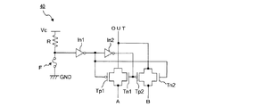
図5は、本発明の半導体集積回路に使用される切替え器40の一例を示す回路図である。本例においては、フューズの溶断により、2つの入力信号A及びBを選択的に切替えて一方を出力する。
FIG. 5 is a circuit diagram showing an example of the
入力信号Aは、PチャンネルのトランジスタTp1とNチャンネルのトランジスタTn1とが並列に接続する一方の端子に入力し、他方の端子が出力端OUTに接続している。入力した信号Bは、PチャンネルのトランジスタTp2とNチャンネルのトランジスタTn2とが並列に接続する一方の端子に入力し、他方の端子が出力端OUTに接続している。 The input signal A is input to one terminal where the P-channel transistor Tp1 and the N-channel transistor Tn1 are connected in parallel, and the other terminal is connected to the output terminal OUT. The input signal B is input to one terminal where the P-channel transistor Tp2 and the N-channel transistor Tn2 are connected in parallel, and the other terminal is connected to the output terminal OUT.
抵抗RとフューズFは直列接続し、電圧VcとGND間に挿入されている。抵抗RとフューズFとの接続点は、第1インバータIn1の入力端に接続している。第1インバータIn1の出力端は第2インバータIn2の入力端とトランジスタTp1のゲート及びトランジスタTn2のゲートに接続している。第2インバータIn2の出力端はトランジスタTn1のゲートとトランジスタTp2のゲートに接続している。 The resistor R and the fuse F are connected in series and are inserted between the voltage Vc and GND. A connection point between the resistor R and the fuse F is connected to an input terminal of the first inverter In1. The output terminal of the first inverter In1 is connected to the input terminal of the second inverter In2, the gate of the transistor Tp1, and the gate of the transistor Tn2. The output terminal of the second inverter In2 is connected to the gate of the transistor Tn1 and the gate of the transistor Tp2.
Vcに電圧が印加されているときは、第1インバータIn1の入力端はLレベル、出力端はHレベルとなり、第2インバータIn2の入力端はHレベル、出力端はLレベルとなる。そのため、トランジスタTp1は、ゲートがHレベルとなってオフ状態となり、トランジスタTn1は、ゲートがLレベルとなって同様にオフ状態となる。他方、トランジスタTp2は、ゲートがLレベルとなってオン状態となり、トランジスタTn2はゲートがHレベルとなって同様にオン状態となる。従って、信号Aは遮断され、信号Bが出力される。 When a voltage is applied to Vc, the input terminal of the first inverter In1 is L level and the output terminal is H level, the input terminal of the second inverter In2 is H level, and the output terminal is L level. Therefore, the transistor Tp1 is turned off with the gate being at the H level, and the transistor Tn1 is similarly turned off with the gate being at the L level. On the other hand, the transistor Tp2 is turned on with the gate at the L level, and the transistor Tn2 is turned on with the gate at the H level. Therefore, the signal A is cut off and the signal B is output.
レーザ光等により、フューズFを溶断する。すると第1インバータIn1の入力端は反転してHレベルとなる。これにより、各トランジスタTp1、Tn1、Tp2、Tn2のゲートの電位は反転し、信号Bが遮断され、信号Aが出力される。このフューズを用いた切替え器を図2に示す第一及び第二切替え器41〜49及び61〜69に適用することができる。
The fuse F is melted by laser light or the like. Then, the input terminal of the first inverter In1 is inverted and becomes H level. As a result, the potentials of the gates of the transistors Tp1, Tn1, Tp2, and Tn2 are inverted, the signal B is cut off, and the signal A is output. The switching device using this fuse can be applied to the first and
例えば、図2に示す第一及び第二切替え器41〜49、61〜69に図5に示す切替え器40を適用する。第一切替え器41〜49に適用する場合には、信号Bとして自チャンネルのデジタル信号を入力し、信号Aとして自チャンネルよりも下位チャンネルのデジタル信号を入力する。第二切替え器61〜69に適用する場合には、信号Aとして自チャンネルと同じ順番のDA変換器からのアナログ信号と、信号Bとして順番が上位のDA変換器からのアナログ信号を入力する。
For example, the switching
例えば、図4に示すように第3チャンネルのDA変換器53が異常である場合は、第1〜第3チャンネルの第一切替え器41、42及び第二切替え器61、62、63のフューズFをレーザ光等により溶断する。これにより、第1〜第3チャンネルの各チャンネルにおいて、1DA変換器分順番が上位のDA変換器により変換されたアナログ信号を入力して増幅器することになる。
For example, as shown in FIG. 4, when the
なお、上記図5に示すように、フューズFの接続状態から切断状態に切り替えて信号Bから信号Aに切替えた。これに代えて、第1インバータIn1の入力端に他の回路により生成した信号、例えばDA変換器の異常を検出したときに発生させる切替え信号を入力して、信号Aと信号Bとを選択的に切替えるようにしてもよい。 In addition, as shown in the said FIG. 5, it switched from the connection state of the fuse F to the disconnection state, and switched from the signal B to the signal A. Instead, a signal generated by another circuit, for example, a switching signal generated when an abnormality of the DA converter is detected is input to the input terminal of the first inverter In1, and the signal A and the signal B are selectively selected. You may make it switch to.
図4において、第3チャンネルの3番目のDA変換器53が異常である場合について救済する場合を説明したが、より一般的には次の通りである。特定の第jチャンネルに属するj番目のDA変換器が異常であるとする。この場合には、第jチャンネルよりも上位にチャンネルが存在するとき、当該上位の各チャンネルの第一切替え器は、順番が1チャンネル分下位のチャンネルのデジタル信号を自チャンネルのDA変換器に出力する。更に、第jチャンネルよりも順番が下位の各チャンネルの第一切替え器は、自チャンネルのデジタル信号を自チャンネルのDA変換器に出力する。
In FIG. 4, the case where the
第jチャンネルと第jチャンネルよりも順番が上位の各チャンネルの第二切替え器は、切替え信号を入力して、順番が1DA変換器分上位のDA変換器により生成されたアナログ信号を自チャンネルの増幅器に出力する。第jチャンネルよりも順番が下位の各チャンネルの第二切替え器は、自チャンネルのDA変換器から出力されたアナログ信号を自チャンネルの増幅器に出力する。 The second switcher of each channel in the higher order than the jth channel and the jth channel inputs the switching signal, and the analog signal generated by the DA converter higher in order by 1 DA converter is input to the own channel. Output to the amplifier. The second switch of each channel lower in order than the j-th channel outputs the analog signal output from the DA converter of the own channel to the amplifier of the own channel.
<第2実施形態>
図6は、本発明の第2実施形態に係る半導体集積回路10の構成を表す模式図である。本第2実施形態においては、冗長用の0番目のDA変換器50は2つのDA変換器50a、50bから構成されている。本第2実施形態では、第1〜第nチャンネルのDA変換器のうち、2つのDA変換器が異常である場合も、救済することができる。同一の部分又は同一の機能を有する部分には同一の符号を付している。
Second Embodiment
FIG. 6 is a schematic diagram showing the configuration of the semiconductor integrated
ロジック回路2は、ラインバッファ31〜39にシリアルデータを出力する。ラインバッファ31〜39は、第1〜第nチャンネルのパラレルなデジタル信号を生成する。第1チャンネルの第一切替え器41は、第1〜第3チャンネルの各チャンネルのデジタル信号を入力して、いずれかのチャンネルのデジタル信号を選択的に切替えて出力する。第1チャンネルのDA変換器51は、第一切替え器41から入力するデジタル信号をアナログ信号に変換する。第1チャンネルのDA変換器51は順番が1番目のDA変換器である。
The
1番目の順番よりも更に上位の0番目のDA変換器50は、冗長用の2つのDA変換器50a、50bから構成されている。冗長用のDA変換器50aは、第1チャンネルのデジタル信号を入力してアナログ信号に変換し、冗長用のDA変換器50bは、第2チャンネルのデジタル信号をアナログ信号に変換する。第1チャンネルの第二切替え器61は、順位が1番目のDA変換器51から出力されるアナログ信号と、冗長用の順位が0番目の2つのDA変換器50a、50bから出力されるアナログ信号を入力して、いずれかの順番のいずれかのDA変換器からのアナログ信号を出力する。第1チャンネルの増幅器71は、第1チャンネルの第二切替え器61から入力したアナログ信号を増幅して出力する。
The
第2チャンネルの第一切替え器42は、第2〜第4チャンネルのデジタル信号を入力して、いずれかのチャンネルのデジタル信号を選択的に切替えて出力する。第2チャンネルのDA変換器52は、第一切替え器42から入力するデジタル信号をアナログ信号に変換する。第2チャンネルのDA変換器52は順番が2番目のDA変換器である。
The
第2チャンネルの第二切替え器62は、順番が2番目のDA変換器52と順番が1番目のDA変換器51と順番が0番目の冗長用のDA変換器50bから出力されるアナログ信号を入力して、いずれかの順番のアナログ信号を出力する。第2チャンネルの増幅器72は、第2チャンネルの第二切替え器62から入力したアナログ信号を増幅して出力する。
The
第3チャンネルの第一切替え器43は、第3〜第5チャンネルのデジタル信号を入力して、いずれかのチャンネルのデジタル信号を選択的に切替えて出力する。第3チャンネルのDA変換器53は、第一切替え器43から入力するデジタル信号をアナログ信号に変換する。第3チャンネルのDA変換器53は順番が3番目のDA変換器である。
The
第3チャンネルの第二切替え器63は、順番が3番目のDA変換器53と順番が2番目のDA変換器52と順番が1番目のDA変換器51から出力されるアナログ信号を入力して、いずれかの順番のアナログ信号を出力する。第3チャンネルの増幅器73は、第3チャンネルの第二切替え器63から入力したアナログ信号を増幅して出力する。第4チャンネル以降は第3チャンネルと同様である。
The third channel
図7は、図6における半導体集積回路10において、第2チャンネルの2番目のDA変換器52と、第4チャンネルの4番目のDA変換器54が異常である場合の、第一切替え器41〜49、及び、第二切替え器61〜69の接続状態を表す。第3チャンネルの第一切替え器43は、第4チャンネルのラインバッファ34から出力されるデジタル信号を入力して第3チャンネルの順番が3番目のDA変換器53に出力する。第4チャンネルの第二切替え器64は、順番が3番目のDA変換器53から入力したアナログ信号を第4チャンネルの増幅器74に出力する。
7 shows the
第1チャンネルの第一切替え器41は、第3チャンネルのラインバッファ33から入力したデジタル信号を第1チャンネルの順番が1番目のDA変換器51に出力する。第3チャンネルの第二切替え器63は、順番が1番目のDA変換器51から入力したアナログ信号を第3チャンネルの増幅器73に出力する。第2チャンネルの第二切替え器62は、順番が0番目の冗長用のDA変換器50bから入力したアナログ信号を第2チャンネルの増幅器72に出力する。第1チャンネルの第二切替え器61は、順番が0番目の冗長用のDA変換器50aから入力したアナログ信号を第1チャンネルの増幅器71に出力する。
The
また、第4チャンネルよりも順番が下位の各チャンネルにおいては、ラインバッファから出力されたデジタル信号は当該チャンネルの第一切替え器により当該チャンネルのDA変換器に出力される。更に、そのDA変換器から出力されるアナログ信号は当該チャンネルの第二切替え器を介して当該チャンネルの増幅器に出力される。 In each channel lower in order than the fourth channel, the digital signal output from the line buffer is output to the DA converter of the channel by the first switch of the channel. Further, the analog signal output from the DA converter is output to the amplifier of the channel via the second switch of the channel.
このように、2つのDA変換器が異常である場合でも、第一及び第二切替え器により信号経路を冗長回路側へシフトさせて迂回させることにより救済することができる。また、第一及び第二切替え器を切替え信号により駆動すれば、容易に且つ瞬時に救済することができる。更に、異常DA変換器が図7に示すように順番が飛び越える場合でも、また、順番が連続する場合でも救済することができる。 As described above, even when the two DA converters are abnormal, the first and second switching units can be remedied by shifting the signal path to the redundant circuit side to make a detour. Further, if the first and second switching devices are driven by the switching signal, the relief can be easily and instantaneously performed. Further, even when the order of the abnormal DA converter jumps over as shown in FIG. 7 or when the order is continuous, it can be remedied.
上記第2実施形態の場合は、冗長用の0番目のDA変換器として2つのDA変換器50a、50bを構成して、2つの異常DA変換器を救済できるようにしたが、本発明はこれに限定されない。0番目の冗長用のDA変換器としてk個(kは1以上であり、n以下の整数)の冗長用のDA変換器を構成して、k個の異常DA変換器を救済するように構成することができる。
In the case of the second embodiment, the two
この場合に、0番目の冗長用のDA変換器は、01番目から0k番目のk個の冗長用のDA変換器を備える。1番目のDA変換器よりも順番が上位の0k番目の冗長用のDA変換器は、第kチャンネルのデジタルデータを入力する。0k番目の冗長用のDA変換器よりも順番が上位の0(k−1)番目の冗長用のDA変換器は、第(k−1)チャンネルのデジタル信号を入力する。以降同様にして、02番目よりも順番が上位の冗長用の01番目のDA変換器は第1チャンネルのデジタル信号を入力する。 In this case, the 0th redundant DA converter includes the 01st to 0kth k redundant DA converters. The 0k-th redundant DA converter in higher order than the first DA converter inputs the k-th channel digital data. The 0 (k−1) th redundant DA converter, which is higher in order than the 0kth redundant DA converter, inputs the (k−1) th channel digital signal. Thereafter, similarly, the 01st DA converter for redundancy having a higher order than the 02nd inputs the digital signal of the first channel.
更に、第1チャンネルの第一切替え器は、第1〜第(1+k)チャンネルの各デジタル信号を入力して選択的に切替えて第1チャンネルの順番が1番目のDA変換器に出力する。第1チャンネルの第二切替え器は、順番が01〜0k番目の冗長用の各DA変換器と、第1チャンネルの順番が1番目のDA変換器から出力されたアナログ信号を入力し、選択的に切り替えて第1チャンネルの増幅器に出力する。第2チャンネルの第一切替え器は、第2〜第(2+k)チャンネルの各デジタル信号を入力して選択的に切替えて第2チャンネルの順番が2番目のDA変換器に出力する。第2チャンネルの第二切替え器は、順番が02〜0k番目の冗長用のDA変換器と、第1及び第2チャンネルの1番目及び2番目のDA変換器からアナログ信号を入力し、選択的に切替えて第2チャンネルの増幅器に出力する。以降同様にして、第kチャンネルの第一切替え器は、第k〜(1+2k)チャンネルの各デジタル信号を入力して選択的に切替えて第kチャンネルのk番目のDA変換器に出力する。第kチャンネルの第二切替え器は、順番が0k番目の冗長用のDA変換器と、第1〜第kチャンネルの1番目〜k番目のDA変換器からのアナログ信号を入力し、選択的に切替えて第kチャンネルの増幅器に出力する。以降同様である。 Further, the first switch of the first channel receives the respective digital signals of the first to (1 + k) channels, selectively switches them, and outputs them to the DA converter whose order of the first channels is the first. The second switcher of the first channel receives each of the DA converters for redundancy having the order of 0 to 0k and the analog signal output from the DA converter having the first order of the first channel. And output to the amplifier of the first channel. The first switch of the second channel receives the digital signals of the second to (2 + k) channels, selectively switches them, and outputs them to the DA converter having the second channel order. The second switch of the second channel receives analog signals from the redundant DA converters in the order of 02 to 0k and the first and second DA converters of the first and second channels, and selectively And output to the second channel amplifier. In the same manner, the k-th channel first switch receives the digital signals of the k-th to (1 + 2k) channels, selectively switches them, and outputs them to the k-th channel k-DA converter. The second switch of the k-th channel inputs the analog signals from the 0k-th redundant DA converter and the first to k-th DA-converters of the first to k-th channels, and selectively Switch to output to the k-th channel amplifier. The same applies thereafter.
このように構成することにより、多数の異常DA変換器が発生した場合でも、第一及び第二切替え器により信号経路を冗長用のDA変換器側に順次切替えることにより、救済することができる。しかし、冗長用のDA変換器の数が増加するにつれて配線が複雑になり、回路面積が増大するので、異常発生確率とDA変換器の冗長作成コストとのコストパフォーマンスを勘案して最適冗長個数を適宜設定すればよい。 With this configuration, even when a large number of abnormal DA converters are generated, the first and second switchers can be remedied by sequentially switching the signal path to the redundant DA converter side. However, as the number of redundant DA converters increases, the wiring becomes more complex and the circuit area increases. Therefore, the optimal redundant number should be determined in consideration of the cost performance of the probability of occurrence of abnormality and the redundancy creation cost of the DA converter. What is necessary is just to set suitably.
<第3実施形態>
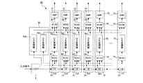
図8は、本発明の第3実施形態に係る半導体集積回路20の構成を表す図である。本実施形態では、増幅器がDA変換器の異常検出器としての機能を有し、異常DA変換器が検出されたときは自動的に冗長用のDA変換器側に配線をシフトして切り替える。
<Third Embodiment>
FIG. 8 is a diagram showing the configuration of the semiconductor integrated
図8に示す半導体集積回路20は、ラインバッファ31〜39、第一切替え器41〜49、DA変換器51〜59、第二切替え器61〜69、及び、増幅器71〜79が含まれ、冗長用のDA変換器50が構成されている。これらの構成及び配線は図2に示す第1実施形態と同様であり、同様に動作する。
The semiconductor integrated
第1チャンネルには、ラインバッファ31、第一及び第二切替え器41、61、DA変換器51、増幅器71の他に、増幅器71からの異常判定信号と順番が下位の第2チャンネルにおいて生成される異常検出信号との論理和を取る論理回路81を備えている。更に、第1チャンネルは、論理回路81からの論理和信号を入力して、第一及び第二切替え器41、61に切替え信号を出力するラッチ回路91を備えている。また、第1チャンネルよりも下位チャンネルの各ラッチ回路92〜99は、順番が1チャンネル分上位のチャンネルに論理和信号を供給する。
In the first channel, in addition to the
各チャンネルの増幅器71〜79の夫々は、ロジック回路2から出力されるTest−Enable信号に応じて、自チャンネルのDA変換器が異常であるか否かを検査し、異常であることを検出したときは、自チャンネルの論理回路に異常判定信号を出力する。また、各チャンネルのラッチ回路91〜99の夫々は、ロジック回路2からのTiming信号を入力して、リセットされる。
Each of the
増幅器71〜79は、例えば、オペアンプとスイッチにより構成することができる。例えば通常動作においては、オペアンプの出力端が反転入力端に接続し、非反転増幅器として機能し、検査モードにおいては、反転入力端を基準電圧に接続し、非反転入力端を自チャンネルの第二切替え器の出力端に接続し、比較器として機能する。また、増幅器71〜79は、後述するように、複数のオペアンプから構成することができる。例えば隣接するDA変換器から出力される2つのアナログ信号を比較することにより、DA変換器の異常を検出するように構成することができる。
The
図8に示す半導体集積回路20は次のように動作する。ロジック回路2は検査モードに入ると各ラッチ回路91〜99にTiming信号を出力して各ラッチ回路91〜99をリセットする。ロジック回路2は更に各増幅器71〜79にTest−Enable信号を出力して各増幅器71〜79を検査モードの接続に切替える。これにより、各増幅器71〜79は自チャンネルのDA変換器の異常を検出する異常検出器として機能する。
The semiconductor integrated
例えば第3チャンネルの増幅器73がDA変換器53の異常を検出したときは、増幅器73はOR回路からなる論理回路83にHレベルの論理和信号を出力する。その他のDA変換器51、52、54〜59は正常なので、各増幅器71、72、74〜79は自チャンネルの論理回路81、82、84〜89にLレベルの信号を出力する。なお、図8には、DA変換器54〜58、増幅器74〜78、論理回路84〜88は図示していない。
For example, when the
第3チャンネルの論理回路83は、Hレベルの異常判定信号を入力してHレベルの論理和信号をラッチ回路93に出力する。ラッチ回路93はHレベルの異常検出信号を第2チャンネルの論理回路82に出力し、論理回路82はラッチ回路92にHレベルの論理和信号を出力する。ラッチ回路92はHレベルの異常検出信号を第1チャンネルの論理回路81に出力し、論理回路81はHレベルの論理和信号をラッチ回路91に出力する。また、第3チャンネルの論理回路83は自チャンネルよりも順番が下位の、例えばラッチ回路99からLレベルの信号を入力している。
The
自チャンネルの論理回路からHレベルの信号を入力した各ラッチ回路91、92、93は、自チャンネルの第一切替え器41、42、43及び第二切替え器61、62、63に対して切替え信号を出力する。各第一切替え器41、42、43は自チャンネルよりも1チャンネル分順番が下位のデジタル信号を入力して自チャンネルのDA変換器に出力する。各第二切替え器61、62、63は自チャンネルのDA変換器よりも順番が上位のDA変換器からアナログ信号を入力して自チャンネルの増幅器に出力する。つまり、第3チャンネル及び第3チャンネル以上の各チャンネルのデジタル信号は1DA変換器分順番が上位のDA変換器によりデジタル信号をアナログ信号に変換して、順番が下位のチャンネルに当該アナログ信号を出力する。
Each of the
第3チャンネルよりも順番が下位のチャンネルのラッチ回路99からは切替え信号が生成されないので、自チャンネルのデジタル信号は自チャンネルのDA変換器によりアナログ信号に変換され、自チャンネルの増幅器により増幅されて出力される。
Since the switching signal is not generated from the
以上のとおり、図8に示す半導体集積回路20は、いずれかのDA変換器が異常である場合には、この異常DA変換器を回避するように信号経路を冗長用のDA変換器側に変更して正常に動作する。また、上記の異常検出機構及び第一及び第二切替え器の自動切換え機構を図6に示す第2実施形態の半導体集積回路10に適用すれば、2個のDA変換器が異常である場合でもこれを自動的に救済することができる。
As described above, the semiconductor integrated
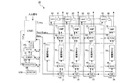
<第4実施形態>
図9は、本発明の第4実施形態に係る半導体集積回路20の構成を表す図である。本第4実施形態では第3実施形態の半導体集積回路にパタン発生用のパタン・タイミングジェネレータ回路等が付加されている。このパタン・タイミングジェネレータ回路等は、検査モードにおいてDA変換器の異常を検出するためのテスト用のパタンデータやテスト用のタイミング信号を生成する。
<Fourth embodiment>
FIG. 9 is a diagram illustrating a configuration of a semiconductor integrated
図9において、ロジック回路2、ラインバッファ31〜39、第一切替え器41〜49、DA変換器51〜59、冗長用のDA変換器50、第二切替え器61〜69、増幅器71〜79、論理回路81〜89、ラッチ回路91〜99の構成は図8に示す第3実施形態と同様なので、説明を省略する。同一の部分又は同一の機能を有する部分には同一の符号を付している。
In FIG. 9,
デテクタ回路DEはVDDの電圧を入力してイネーブル信号及びリセット信号を生成する。オシレータ回路OSはイネーブル信号を入力し、イネーブル信号の極性に応じて発振を開始して発振信号を生成する。デバイダ回路DIは発振信号を入力して分周し、クロック信号CLKを生成する。パタン・タイミング回路PGはパタン・タイミングジェネレータ回路であり、クロック信号CLKを入力してテスト用パタン信号及びテスト用動作タイミング信号を生成する。 The detector circuit DE receives the VDD voltage and generates an enable signal and a reset signal. The oscillator circuit OS receives an enable signal, starts oscillation according to the polarity of the enable signal, and generates an oscillation signal. The divider circuit DI receives the oscillation signal and divides it to generate the clock signal CLK. The pattern timing circuit PG is a pattern timing generator circuit that receives the clock signal CLK and generates a test pattern signal and a test operation timing signal.
上記回路は次にように動作する。電源が投入され、VDDが立ち上がったことをデテクタ回路DEが検知してイネーブル信号及びリセット信号を生成する。オシレータ回路OSはデテクタ回路DEのイネーブル信号を入力して発振を開始し、デバイダ回路DI、パタン・タイミング回路PG及びロジック回路2はデテクタ回路DEのリセット信号を入力してリセットされる。発振を開始したオシレータ回路OSは発振信号をデバイダ回路DIへ出力し、デバイダ回路DIはこの発振信号を入力して分周し、クロック信号CLKを生成し、ロジック回路2及びパタン・タイミング回路PGへ出力する。
The circuit operates as follows. The detector circuit DE detects that the power is turned on and VDD has risen, and generates an enable signal and a reset signal. The oscillator circuit OS receives the enable signal of the detector circuit DE and starts oscillation , and the divider circuit DI, the pattern timing circuit PG, and the
パタン・タイミング回路PGはクロック信号CLKを用いてテスト用のパタン信号と、テスト用のタイミング信号を生成してロジック回路2へ出力する。ロジック回路2は、Test−Enable信号を生成して増幅器71〜79に出力し、Timing信号を生成してラッチ回路91〜99をリセットし、テスト用のパタンデータを生成してラインバッファ31〜39へ出力する。増幅器71〜79はTest−Enable信号を入力することによりDA変換器51〜59の異常を検出する異常検出器として機能する。テスト完了時にはイネーブル信号をHレベルからLレベルへ切替えて、オシレータ回路OSの発振を停止する。これにより、検査モードは終了する。
The pattern timing circuit PG generates a test pattern signal and a test timing signal using the clock signal CLK, and outputs them to the
この構成により、外部から制御信号やテスト用のパタン信号等を必要とせずに、DA変換器51〜59の異常を検出することができ、更に、いずれかのDA変換器が異常の場合には、自動的に冗長救済を図ることができる。
With this configuration, it is possible to detect an abnormality in the
なお、上記の回路構成において、VDDを検出するためのデテクタ回路DEを設けて、電源投入時に検査モードが実行されるように構成したが、デテクタ回路DEを除去して、外部からテスト制御信号を入力することで、検査モードが実行されるようにしてもよい。 In the above circuit configuration, the detector circuit DE for detecting VDD is provided and the inspection mode is executed when the power is turned on. However, the detector circuit DE is removed, and a test control signal is externally supplied. The inspection mode may be executed by inputting.
<第5実施形態>
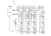
図10は、本発明の第5実施形態に係る半導体集積回路30の構成を表す図である。本第5実施形態においては、各チャンネルが4つのサブチャンネルにより構成されている。同一の部分又は同一の機能を有する部分には同一の符号を付している。
<Fifth Embodiment>
FIG. 10 is a diagram showing a configuration of a semiconductor integrated
図10に示すように、各チャンネルは4つのサブチャンネルAch〜Dchから構成されている。各チャンネルは、4つのサブチャンネルに対応する4つのサブラインバッファ、4つのサブ第一切替え器、4つのサブDA変換器、4つのサブ第二切替え器、4つのサブ増幅器、1つの論理回路、1つのラッチ回路から構成されている。各チャンネルの各サブチャンネルは、1つのサブラインバッファ、1つのサブ第一切替え器、1つのサブDA変換器、1つのサブ第二切替え器、1つのサブ増幅器から構成されている。冗長用のDA変換器50は4つのサブDA変換器により構成されている。この冗長用の4つのサブDA変換器の夫々は、第1チャンネルの4つのサブチャンネルの夫々対応するサブラインバッファからデジタル信号を入力する。
As shown in FIG. 10, each channel is composed of four subchannels Ach to Dch. Each channel includes four subline buffers corresponding to four subchannels, four subfirst switchers, four subDA converters, four subsecond switchers, four subamplifiers, one logic circuit, It consists of two latch circuits. Each subchannel of each channel is composed of one subline buffer, one subfirst switch, one subDA converter, one subsecond switch, and one subamplifier. The
例えば第1チャンネルのサブチャンネルAchに注目して説明する。サブ第一切替え器は自サブチャンネルAchのサブラインバッファと第2チャンネルのサブチャンネルAchからのデジタル信号とを入力して選択的に切替えて自サブチャンネルのサブDA変換器へ出力する。サブチャンネルAchのサブDA変換器は入力したデジタル信号をアナログ信号に変換する。サブチャンネルAchのサブ第二切替え器は、自サブチャンネルAchのデジタル信号をアナログ信号に変換する冗長用のサブDA変換器と自サブチャンネルAchのサブDA変換器からのアナログ信号を入力して自サブチャンネルAchのサブ増幅器へ選択的に切替えて出力する。他のサブチャンネルも同様の構成を備えている。 For example, the description will be made by paying attention to the subchannel Ach of the first channel. The first sub-switcher inputs the sub-line buffer of the own sub-channel Ach and the digital signal from the second-channel sub-channel Ach, selectively switches them, and outputs them to the sub-DA converter of the own sub-channel. The sub D / A converter of the sub channel Ach converts the input digital signal into an analog signal. The sub second switch of the subchannel Ach inputs the analog signal from the redundant sub DA converter that converts the digital signal of the own subchannel Ach into an analog signal and the analog signal from the sub DA converter of the own subchannel Ach. The signal is selectively switched to the sub-channel Ach sub-amplifier for output. Other subchannels have the same configuration.
第2チャンネルよりも順番が下位のチャンネルでは次の通りである。各サブチャンネルのサブ第二切替え器は、1チャンネル分順番が上位のチャンネルの対応するサブチャンネルのサブDA変換器と自サブチャンネルのサブDA変換器からのアナログ信号を選択的に切替えて自サブチャンネルのサブ増幅器へ出力する。なお、説明の都合上図10では3チャンネルの構成を表しているが、実際は更に多数のチャンネルを備えている。 It is as follows in the channel lower in order than the second channel. The sub-second switcher for each subchannel selectively switches the analog signal from the corresponding subchannel sub-DA converter of the higher-order channel and the sub-DA converter of the own subchannel by one channel. Output to the channel sub-amplifier. For convenience of explanation, FIG. 10 shows a three-channel configuration, but actually, a larger number of channels are provided.
図11(a)は第2チャンネルを抜き出して示した図である。図11(b)は通常使用状態である通常モードのときの増幅器72に構成されるスイッチSW1〜SW4の接続状態を表す。図11(c)は、DA変換器52を検査する検査モード1のときのSW1〜SW4の接続状態を表す。図11(d)は、DA変換器52を検査する検査モード2のときのスイッチSW1〜SW4の接続状態を表す。なお、スイッチSW1、SW3は第三切替え器に相当し、スイッチSW2、SW4は第四切替え器に相当する。
FIG. 11A shows the second channel extracted. FIG. 11B shows a connection state of the switches SW1 to SW4 configured in the
図11(a)に示すように、各サブチャンネルAch〜Dchは、サブ増幅器としてオペアンプOPa〜OPdを備えている。サブチャンネルAch、BchのオペアンプOPa、OPbは、出力端が反転入力端に接続され、非反転入力端にサブ第二切替え器からのアナログ信号を入力する非反転増幅器を構成している。サブチャンネルCchのオペアンプOPcは、出力端と反転入力端との間にスイッチSW1が挿入され、反転入力端及び非反転入力端とサブチャンネルBch及びCchからのサブ第二切替え器の出力との間にスイッチSW2が挿入されている。サブチャンネルDchのオペアンプOPdは、出力端と反転入力端との間にスイッチSW3が挿入され、反転入力端及び非反転入力端とサブチャンネルAch及びDchのサブ第二切替え器からの出力との間にスイッチSW4が挿入されている。 As shown in FIG. 11A, each of the subchannels Ach to Dch includes operational amplifiers OPa to OPd as subamplifiers. The operational amplifiers OPa and OPb of the sub-channels Ach and Bch constitute a non-inverting amplifier that has an output terminal connected to the inverting input terminal and inputs an analog signal from the sub second switch to the non-inverting input terminal. In the subchannel Cch operational amplifier OPc, the switch SW1 is inserted between the output terminal and the inverting input terminal, and between the inverting input terminal and the non-inverting input terminal and the output of the sub second switch from the subchannels Bch and Cch. The switch SW2 is inserted in In the subchannel Dch operational amplifier OPd, the switch SW3 is inserted between the output terminal and the inverting input terminal, and between the inverting input terminal and the non-inverting input terminal and the output from the sub-second switcher of the subchannels Ach and Dch. The switch SW4 is inserted in
論理回路82はNAND回路とOR回路から構成されている。NAND回路はオペアンプOPcとオペアンプOPdの出力の否定論理積をOR回路に出力する。OR回路は、NAND回路からの否定論理積と順番が下位の第3チャンネルからの異常検出信号との論理和をラッチ回路92に出力する。以下、増幅器72の動作及びDA変換器の異常検出方法を図11(b)〜(c)に基づいて具体的に説明する。
The
図11(b)は、通常モードのときのスイッチSW1〜SW4の接続状態を表す。スイッチSW1及びSW3は接続状態となり、オペアンプOPc及びOPdの夫々の出力端と反転入力端が接続し、オペアンプOPc及びOPdは非反転増幅器として動作する。また、スイッチSW2及びSW4は、サブチャンネルCch及びDchの各サブDA変換器により変換されたアナログ信号をオペアンプOPc及びOPdの非反転入力端に入力するように切り替わる。その結果、オペアンプOPc、OPdは、オペアンプOPa、OPbと同等の電流増幅器として機能する。 FIG. 11B shows the connection state of the switches SW1 to SW4 in the normal mode. The switches SW1 and SW3 are connected, the output terminals of the operational amplifiers OPc and OPd are connected to the inverting input terminal, and the operational amplifiers OPc and OPd operate as a non-inverting amplifier. The switches SW2 and SW4 are switched so that the analog signals converted by the sub-DA converters of the subchannels Cch and Dch are input to the non-inverting input terminals of the operational amplifiers OPc and OPd. As a result, the operational amplifiers OPc and OPd function as current amplifiers equivalent to the operational amplifiers OPa and OPb.
検査モードに入ると、ロジック回路2は、増幅器72にTest−Enable信号を出力してスイッチSW1〜SW4をセットするとともに、Timing信号によりラッチ回路92をリセットし、ラインバッファ32にテストデータを出力する。
When entering the inspection mode, the
図11(c)は最初の検査モード1におけるスイッチSW1〜SW4の接続状態を表す。スイッチSW1は開状態となり、スイッチSW2は、サブチャンネルBchのサブ第二切替え器の出力がオペアンプOPcの反転入力端に入力し、自サブチャンネルCchのサブ第二切替え器の出力が非反転入力端に入力する接続状態に切り替わる。従って、オペアンプOPcは、サブチャンネルBchとCchの2つのサブDA変換器の出力電圧を比較する比較器として動作する。更に、スイッチSW3は開状態となり、スイッチSW4は、サブチャンネルAchのサブ第二切替え器の出力がオペアンプOPdの反転入力端に入力し、自サブチャンネルDchのサブ第二切替え器の出力が非反転入力端に入力する接続状態に切り替わる。従って、オペアンプOPdは、サブチャンネルAchとDchの2つのサブDA変換器の出力電圧を比較する比較器として動作する。
FIG. 11C shows the connection state of the switches SW1 to SW4 in the
ロジック回路2はラインバッファ32にテストデータを出力し、各サブチャンネルAch、Bch、Cch、Dchに対して夫々電圧Va、Vb、Vc、Vdを設定する。この場合にVcはVbより微小電圧δcb高く、VdはVaよりも微小電圧δda高く設定し、この関係を維持して電圧Va、Vb、Vc、Vdを変化させる。各サブDA変換器が正常に動作する場合には、各サブDA変換器により変換された電圧は常にVc>Vb、Vd>Vaの関係が維持される。従って、オペアンプOPc及びOPdからはHレベルの信号が出力され、NAND回路からはLレベルが出力されて、異常がないことを表す。一方、各サブチャンネルのサブDA変換器から出力される電圧の関係が、Vc<VbやVd<Vaとなる場合は、オペアンプOPc又はOPdのいずれか又は両方の出力がLレベルとなる。その結果、NAND回路の出力はHレベルに反転し、これに伴いOR回路の出力もHレベルに反転して、いずれかのDA変換器が異常であることを知らせる。
The
しかし、例えば、サブチャンネルBchのサブDA変換器が故障して、設定された電圧Vbよりも常に低い電圧を発生させる場合がある。また、サブチャンネルAchのサブDA変換器が故障して、設定された電圧Vaよりも常に低い電圧を発生させる場合がある。これらの場合には、各サブDA変換器により変換された電圧は常にVc>Vb、Vd>Vaの関係を維持することになり、異常を検出できない場合が存在する。 However, for example, the sub D / A converter of the sub channel Bch may break down and generate a voltage that is always lower than the set voltage Vb. Further, the sub-DA converter of the sub-channel Ach may break down and generate a voltage that is always lower than the set voltage Va. In these cases, the voltage converted by each sub DA converter always maintains the relationship of Vc> Vb and Vd> Va, and there is a case where an abnormality cannot be detected.
こそで、次の検査モード2においては、図11(d)に示すようにスイッチSW2及びSW4の接続状態を切替える。即ち、サブチャンネルCchのVcをオペアンプOPcの反転入力端に、サブチャンネルBchのVbをオペアンプOPcの非反転入力端に入力する。また、サブチャンネルDchのVdをオペアンプOPdの反転入力端に、サブチャンネルAchのVaをオペアンプOPdの非反転入力端に入力する。
In the
更に、ロジック回路2は、VbをVcより微小電圧δbc高く、VaをVdよりも微小電圧δad高く設定し、この関係を維持して電圧Va、Vb、Vc、Vdを変化させる。各サブDA変換器が正常に動作する場合には、各サブDA変換器により変換された電圧は常にVb>Vc、Va>Vdの関係を維持する。従って、オペアンプOPc及びOPdからはHレベルの信号が出力され、NAND回路からはLレベルが出力されて、異常がないことを表す。
Further, the
一方、各サブチャンネルのサブDA変換器から出力される電圧関係が、Vb<VcやVa<Vdとなる場合は、オペアンプOPc又はOPdのいずれか又は両方の出力がLレベルとなる。その結果、NAND回路の出力はHレベルに反転し、OR回路の出力もHレベルに反転して、いずれかのサブDA変換器が異常であることを知らせる。 On the other hand, when the voltage relationship output from the sub D / A converter of each sub channel is Vb <Vc or Va <Vd, the output of either or both of the operational amplifiers OPc and OPd is L level. As a result, the output of the NAND circuit is inverted to H level, and the output of the OR circuit is also inverted to H level to notify that any of the sub DA converters is abnormal.
上記検査モード1及び検査モード2において異常が検出されると、OR回路からHレベルの信号を入力したラッチ回路92は、第一切替え器42及び第二切替え器62に切替え信号を出力するとともに、順番が上位の第1チャンネルに異常検出信号を出力する。第1チャンネルの論理回路81は、ラッチ回路92からHレベルの異常検出信号を入力してそのOR回路がHレベルの和信号を出力する。第1チャンネルのラッチ回路91は、Hレベルの和信号を入力して、第一切替え器41及び第二切替え器61に切替え信号を出力する。
When an abnormality is detected in the
これにより、第1チャンネルの各サブ第一切替え器は、第2チャンネルの各サブチャンネル用のデジタル信号を自サブチャンネルの各サブDA変換器へ出力する。第1チャンネルの各サブ第二切替え器は、冗長用の各サブDA変換器により変換されたアナログ信号を自サブチャンネルの各サブ増幅器へ出力する。従って、第2チャンネルの各サブチャンネルのデジタル信号は第1チャンネルのDA変換器51により変換され、第2チャンネルの第二切替え器62を介して増幅器72(オペアンプOPa〜OPd)により増幅され、出力される。また、第1チャンネルの各サブチャンネルのデジタル信号は冗長用のDA変換器50により変換され、第1チャンネルの第二切替え器61を介して増幅器71(オペアンプOPa〜OPd)により増幅され、出力される。
Thereby, each sub 1st changer of a 1st channel outputs the digital signal for each subchannel of a 2nd channel to each sub DA converter of an own subchannel. Each sub-second switch in the first channel outputs the analog signal converted by each sub-DA converter for redundancy to each sub-amplifier in its own sub-channel. Accordingly, the digital signal of each sub-channel of the second channel is converted by the
このように、増幅器をオペアンプOPにより構成し、通常動作では電流増幅器として機能させ、検査モードにおいては比較器として機能させることにより、比較的簡単な構成でDA変換器の異常を検出できるとともに、冗長回路を設けて冗長救済することができる。 In this way, the amplifier is composed of the operational amplifier OP, and functions as a current amplifier in normal operation, and functions as a comparator in the inspection mode, so that an abnormality of the DA converter can be detected with a relatively simple configuration, and redundant. A circuit can be provided to provide redundant relief.
なお、本第5実施形態の半導体集積回路30は、液晶パネルの信号駆動回路に適用するのが好適である。液晶パネルでは、液晶の劣化、信頼性低下を防止するために、液晶層に対して共通電極を基準として正負の交番電圧を印加する。例えば、サブチャンネルAchとDchに正側(又は負側)の電圧、サブチャンネルBchとCchに負側(又は正側)の電圧を与える。そして、サブチャンネルAchとBchの出力を交番させ、サブチャンネルCchとDchの出力を交番させて液晶パネルに交番電圧を与えることができる。
Note that the semiconductor integrated
なお、本第5実施形態においては、4つのサブチャンネルを1チャンネルとして取り扱い、4つのサブチャンネルのいずれかのDA変換器が異常である場合に、1チャンネル単位で冗長用のDA変換器側に接続をシフトして冗長救済を行う。この場合に、各サブチャンネルを独立した1チャンネルとみなすこともできる。つまり、各第一切替え器は自チャンネルのデジタル信号と順番が4チャンネル分下位のデジタル信号とのいずれかを選択的に切替えて自チャンネルのDA変換器に出力する。また、各第二切替え器は、自チャンネルのDA変換器により変換されたアナログ信号と順番が4チャンネル分上位のDA変換器により変換されたアナログ信号とのいずれかを選択的に切替えて自チャンネルの増幅器に出力する、とみなすことができる。 In the fifth embodiment, four subchannels are handled as one channel, and if any DA converter of any of the four subchannels is abnormal, the redundant DA converter side is set in units of one channel. Redundant relief is performed by shifting the connection. In this case, each subchannel can be regarded as an independent channel. That is, each first switch selectively switches between the digital signal of its own channel and the digital signal lower in order by four channels, and outputs it to the DA converter of its own channel. Each second switch selectively switches between the analog signal converted by the DA converter of its own channel and the analog signal converted by the DA converter which is higher in order by four channels. Can be regarded as being output to the amplifier.
図12は、例えば図9に示す第4実施形態や図10に示す第5実施形態などの半導体集積回路における検査モードのタイミングチャート図を示す。電源が投入されVDDが印加されると、デテクタ回路DEがイネーブル信号やリセット信号を出力し、オシレータ回路OSからOscillator OUT信号が出力される。デバイダ回路DIからクロック信号CLKが出力される。ロジック回路2は、増幅器71〜79とラッチ回路91〜99に与えるTEST/Test_Enable信号をLレベルからHレベルへ反転させ、検査モードを開始する。ロジック回路2は、同時にテストデータからなるData信号をラインバッファ31〜39に与える。増幅器71〜79は検査モードにおいてはDA変換器51〜59の異常検出器として機能し、異常が検出されると当該増幅器のAMP out信号がLレベルからHレベルに反転する。すると、論理回路の出力がLレベルからHレベルに反転し、ラッチ回路のRS_Latch OUT信号がLレベルからHレベルに反転し、当該チャンネル及びこのチャンネルよりも順番が上位のチャンネルの第一切替え器及び第二切替え器に出力される。
FIG. 12 is a timing chart of an inspection mode in a semiconductor integrated circuit such as the fourth embodiment shown in FIG. 9 or the fifth embodiment shown in FIG. When power is turned on and VDD is applied, the detector circuit DE outputs an enable signal and a reset signal, and the oscillator circuit OS outputs an Oscillator OUT signal. A clock signal CLK is output from the divider circuit DI. The
<第6実施形態>
図13は、本発明の第6実施形態に係る液晶駆動回路を表す模式図である。液晶駆動回路は、液晶パネル27の走査線を駆動する走査線ドライバ26と、信号線を駆動する信号線ドライバ25と、これらのドライバに駆動信号を供給するロジック回路2などから構成されている。信号線ドライバ25は、第1〜第5実施形態において説明した半導体集積回路により構成され、この半導体集積回路の第1〜第nチャンネルから出力されるアナログ信号が液晶パネル27の各信号線に供給される。
<Sixth Embodiment>
FIG. 13 is a schematic diagram showing a liquid crystal driving circuit according to the sixth embodiment of the present invention. The liquid crystal driving circuit includes a
特に、液晶パネル27では信号線が500本以上形成されており、そのうち1本の信号線に供給される映像信号が異常であると、ライン欠陥として見えるようになる。本液晶駆動回路はDA変換器が異常となった場合でも冗長救済することができるので、液晶駆動回路のコスト低減に大きく寄与することができる。
In particular, in the
1、10、20、30 半導体集積回路
2 ロジック回路
31〜39 ラインバッファ
41〜49 第一切替え器
50 冗長用のDA変換器
51〜59 DA変換器
61〜69 第二切替え器
71〜79 増幅器
81〜89 論理回路
91〜99 ラッチ回路
1, 10, 20, 30 Semiconductor integrated
Claims (6)
αチャンネルのデジタル信号とβチャンネルのデジタル信号を選択的に切替えて出力するαチャンネルの第一切替え器と、
αチャンネルの第一切替え器から入力するデジタル信号をアナログ信号に変換するαチャンネルのDA変換器と、
βチャンネルのデジタル信号をアナログ信号に変換するβチャンネルのDA変換器と、
αチャンネルのデジタル信号をアナログ信号に変換する冗長用のDA変換器と、
前記冗長用のDA変換器から入力するアナログ信号とαチャンネルのDA変換器から入力するアナログ信号を選択的に切替えて出力するαチャンネルの第二切替え器と、
αチャンネルのDA変換器からのアナログ信号とβチャンネルのDA変換器からのアナログ信号を選択的に切替えて出力するβチャンネルの第二切替え器と、
αチャンネルの第二切替え器から入力したアナログ信号を増幅するαチャンネルの増幅器と、
βチャンネルの第二切替え器から入力したアナログ信号を増幅するβチャンネルの増幅器と、を備え、
前記αチャンネルは、順番が上位の第1チャンネルから順番が下位の第n(nは2以上の整数)チャンネルを含み、前記ラインバッファは前記第1〜第nチャンネル用のデジタル信号を生成し、
前記第1〜第nの各チャンネルは、第一切替え器と、DA変換器と、第二切替え器と、増幅器を含み、
前記冗長用のDA変換器を順番が0番目の最上位とし、前記第1〜第nの各チャンネルのDA変換器を順番が上位の1番目から順番が下位のn番目とし、前記βチャンネルのDA変換器を順番が最下位とした場合に、
第1〜第nの各チャンネルの第一切替え器は、自チャンネルのデジタル信号と自チャンネルよりも順番が下位のチャンネルのデジタル信号とを選択的に切替えて自チャンネルのDA変換器へ出力し、
第1〜第nの各チャンネルの第二切替え器は、自チャンネルのDA変換器から出力されるアナログ信号と順番が上位のDA変換器から出力されるアナログ信号とを選択的に切替えて自チャンネルの増幅器へ出力し、
各チャンネルの増幅器は、自チャンネルのDA変換器が異常であるか否かを検査して異常判定信号を生成する異常検出器として機能し、
前記の各チャンネルは、
自チャンネルの増幅器により生成された異常判定信号と、自チャンネルよりも順番が下位のチャンネルが存在する場合に当該下位のチャンネルにより生成された異常検出信号との論理和をとる論理回路と、
自チャンネルの論理回路から入力した論理和信号を保持し、自チャンネルよりも上位のチャンネルが存在する場合に当該上位のチャンネル用の異常検出信号と、自チャンネルの第一切替え器及び第二切替え器に与える切替え信号とを生成するラッチ回路と、を更に備える半導体集積回路。 A line buffer that converts serial data into parallel α-channel digital signals and β-channel digital signals;
a first α channel switcher that selectively switches between an α channel digital signal and a β channel digital signal,
an α channel DA converter that converts a digital signal input from the α channel first switch to an analog signal;
a β-channel DA converter for converting a β-channel digital signal into an analog signal;
a redundant DA converter that converts an alpha channel digital signal into an analog signal;
An α channel second switch for selectively switching and outputting an analog signal input from the redundant DA converter and an analog signal input from the α channel DA converter;
a β-channel second switch for selectively switching and outputting an analog signal from the α-channel DA converter and an analog signal from the β-channel DA converter;
an α channel amplifier that amplifies the analog signal input from the α channel second switch;
a β channel amplifier that amplifies the analog signal input from the β channel second switch ,
The α channel includes an n-th channel (n is an integer equal to or greater than 2) in order from the first channel in the higher order, and the line buffer generates digital signals for the first to n-th channels,
Each of the first to n-th channels includes a first switch, a DA converter, a second switch, and an amplifier.
The redundant DA converter is the highest in the 0th order, the DA converters in the first to nth channels are in the order from the first to the lower nth, and the β channel When the DA converter is in the lowest order,
The first switch of each of the first to n-th channels selectively switches between the digital signal of the own channel and the digital signal of the channel lower in order than the own channel and outputs to the DA converter of the own channel,
The second switch for each of the first to n-th channels selectively switches between the analog signal output from the DA converter of the own channel and the analog signal output from the higher order DA converter. Output to the amplifier
The amplifier of each channel functions as an abnormality detector that generates an abnormality determination signal by checking whether or not the DA converter of its own channel is abnormal,
Each of the above channels is
A logic circuit that performs a logical sum of the abnormality determination signal generated by the amplifier of the own channel and the abnormality detection signal generated by the lower channel when there is a lower order channel than the own channel;
Holds the logical sum signal input from the logic circuit of the own channel, and when there is a channel higher than the own channel, the abnormality detection signal for the higher channel, the first switcher and the second switcher of the own channel And a latch circuit for generating a switching signal to be applied to the semiconductor integrated circuit.
前記第1〜第nの各チャンネルの第二切替え器は、自チャンネルのDA変換器から出力されるアナログ信号と順番が1DA変換器分上位のDA変換器から出力されるアナログ信号とを選択的に切替えて自チャンネルの増幅器へ出力する、ことを特徴とする請求項1に記載の半導体集積回路。 The second switch of each of the first to n-th channels selectively selects an analog signal output from the DA converter of its own channel and an analog signal output from a DA converter higher in order by 1 DA converter. 2. The semiconductor integrated circuit according to claim 1, wherein the output is switched to the amplifier of the own channel.
前記第jチャンネル、及び、前記第jチャンネルより順番が上位のチャンネルが存在する場合において当該上位の各チャンネルの第二切替え器は、前記切替え信号に応じて順番が上位のDA変換器により生成されたアナログ信号を自チャンネルの増幅器に出力するとともに、前記第jチャンネルより順番が下位の各チャンネルの第二切替え器は、自チャンネルのDA変換器から出力されたアナログ信号を自チャンネルの増幅器に出力する請求項1又は2に記載の半導体集積回路。 In the case where there is a channel higher in order than the j-th channel and the j-th channel, the second switch of each higher-order channel is generated by a DA converter having a higher order in accordance with the switching signal. The analog signal output from the DA converter of the own channel is output to the amplifier of the own channel. The semiconductor integrated circuit according to claim 1 or 2.
各チャンネルの第一切替え器は、第1〜第xのサブ第一切替え器を含み、 The first switch of each channel includes first to xth sub first switches,
各チャンネルのDA変換器は、第1〜第xのサブDA変換器を含み、 Each channel DA converter includes first to xth sub DA converters,
前記第0番目のDA変換器は、第1〜第xのサブDA変換器を含み、 The zeroth DA converter includes first to xth sub DA converters,
各チャンネルの第二切替え器は、第1〜第xのサブ第二切替え器を含み、 The second switch of each channel includes first to xth sub-second switches,
各チャンネルの増幅器は、第1〜第xのサブ増幅器を含み、 Each channel amplifier includes first to xth sub-amplifiers;
各チャンネルの第pサブ第一切替え器(pは1からx以下の整数)は、自チャンネルの第pサブチャンネルのデジタル信号と、自チャンネルよりも順番が下位のチャンネルが存在する場合の当該下位のチャンネルの第pサブチャンネルのデジタル信号とを選択的に切替えて自チャンネルの第pサブDA変換器に出力し、 The p-th sub first switcher (p is an integer from 1 to x) of each channel is the subordinate when there is a digital signal of the p-th subchannel of the own channel and a channel whose order is lower than the own channel. Selectively switching the digital signal of the p-th sub-channel of the current channel to the p-th sub-DA converter of the own channel,
各チャンネルの第pサブ第二切替え器は、自チャンネルの第pサブDA変換器から出力されるアナログ信号と、自チャンネルよりも順番が上位のチャンネルが存在する場合において当該上位のチャンネルの第pサブDA変換器から出力されるアナログ信号とを選択的に切替えて出力し、 The p-th sub-second switch for each channel is configured so that the analog signal output from the p-th sub-DA converter of its own channel and the p-th sub channel of the higher-order channel when there is a higher-order channel than the own channel. Selectively switch the analog signal output from the sub DA converter,
各チャンネルの第pサブ増幅器は、自チャンネルの第pサブ第二切替え器から出力されるアナログ信号を増幅する請求項1〜3のいずれか1項に記載の半導体集積回路。 4. The semiconductor integrated circuit according to claim 1, wherein the p-th sub-amplifier of each channel amplifies the analog signal output from the p-th sub-second switch of the own channel.
前記第1〜第nのサブチャンネルのうちの所定のサブチャンネルは、 A predetermined sub-channel among the first to n-th sub-channels is
前記オペアンプを増幅器の機能から比較器の機能に切替える第三切替え器と、 A third switch for switching the operational amplifier from an amplifier function to a comparator function;
前記オペアンプの入力を、自サブチャンネルの第二切替え器からの入力から、自サブチャンネルの第二切替え器からの入力と他のサブチャンネルの第二切替え器からの入力の並列入力に切替える第四切替え器と、を備えることを特徴とする請求項4に記載の半導体集積回路。 The fourth operational amplifier switches the input of the operational amplifier from the input from the second switch of the own subchannel to the parallel input of the input from the second switch of the own subchannel and the input from the second switch of the other subchannel. The semiconductor integrated circuit according to claim 4, further comprising a switch.
第iチャンネル(iは1からn−1の整数)のデジタル信号と第i+1チャンネルのデジタル信号とを選択的に切替えて出力する第iチャンネルの第一切替え器と、 A first switch of the i-th channel for selectively switching and outputting the digital signal of the i-th channel (i is an integer from 1 to n-1) and the digital signal of the i + 1-th channel;
第1チャンネルのデジタル信号をアナログ信号に変換する冗長用の0番目のDA変換器と、 A 0th DA converter for redundancy that converts the digital signal of the first channel into an analog signal;
第iチャンネルの第一切替え器から出力されるデジタル信号をアナログ信号に変換する第iチャンネルに属するi番目のDA変換器と、 An i-th DA converter belonging to the i-th channel for converting a digital signal output from the first switch of the i-th channel into an analog signal;
i番目のDA変換器から出力されるアナログ信号とi−1番目のDA変換器から出力されるアナログ信号を選択的に切替えて出力する第iチャンネルの第二切替え器と、 a second switch of the i-th channel for selectively switching the analog signal output from the i-th DA converter and the analog signal output from the (i-1) -th DA converter;
第iチャンネルの第二切替え器から出力されるアナログ信号を増幅する第iチャンネルの増幅器と、を備え、 An i-th channel amplifier for amplifying an analog signal output from the i-th channel second switch,
前記αチャンネルは、順番が上位の第1チャンネルから順番が下位の第n(nは2以上の整数)チャンネルを含み、前記ラインバッファは前記第1〜第nチャンネル用のデジタル信号を生成し、 The α channel includes an n-th channel (n is an integer equal to or greater than 2) in order from the first channel in the higher order, and the line buffer generates digital signals for the first to n-th channels,
前記第1〜第nの各チャンネルは、第一切替え器と、DA変換器と、第二切替え器と、増幅器を含み、 Each of the first to n-th channels includes a first switch, a DA converter, a second switch, and an amplifier.
前記冗長用のDA変換器を順番が0番目の最上位とし、前記第1〜第nの各チャンネルのDA変換器を順番が上位の1番目から順番が下位のn番目とし、前記βチャンネルのDA変換器を順番が最下位とした場合に、 The redundant DA converter is the highest in the 0th order, the DA converters in the first to nth channels are in the order from the first to the lower nth, and the β channel When the DA converter is in the lowest order,
第1〜第nの各チャンネルの第一切替え器は、自チャンネルのデジタル信号と自チャンネルよりも順番が下位のチャンネルのデジタル信号とを選択的に切替えて自チャンネルのDA変換器へ出力し、 The first switch of each of the first to n-th channels selectively switches between the digital signal of the own channel and the digital signal of the channel lower in order than the own channel and outputs to the DA converter of the own channel,
第1〜第nの各チャンネルの第二切替え器は、自チャンネルのDA変換器から出力されるアナログ信号と順番が上位のDA変換器から出力されるアナログ信号とを選択的に切替えて自チャンネルの増幅器へ出力し、 The second switch for each of the first to n-th channels selectively switches between the analog signal output from the DA converter of the own channel and the analog signal output from the higher order DA converter. Output to the amplifier
各チャンネルの増幅器は、自チャンネルのDA変換器が異常であるか否かを検査して異常判定信号を生成する異常検出器として機能し、 The amplifier of each channel functions as an abnormality detector that generates an abnormality determination signal by checking whether or not the DA converter of its own channel is abnormal,
前記の各チャンネルは、 Each of the above channels is
自チャンネルの増幅器により生成された異常判定信号と、自チャンネルよりも順番が下位のチャンネルが存在する場合に当該下位のチャンネルにより生成された異常検出信号との論理和をとる論理回路と、 A logic circuit that performs a logical sum of the abnormality determination signal generated by the amplifier of the own channel and the abnormality detection signal generated by the lower channel when there is a lower order channel than the own channel;
自チャンネルの論理回路から入力した論理和信号を保持し、自チャンネルよりも上位のチャンネルが存在する場合に当該上位のチャンネル用の異常検出信号と、自チャンネルの第一切替え器及び第二切替え器に与える切替え信号とを生成するラッチ回路と、を更に備え、 Holds the logical sum signal input from the logic circuit of the own channel, and when there is a channel higher than the own channel, the abnormality detection signal for the higher channel, the first switcher and the second switcher of the own channel And a latch circuit for generating a switching signal to be applied to
前記増幅器において増幅されたアナログ信号を映像信号とする液晶駆動回路。 A liquid crystal driving circuit using an analog signal amplified by the amplifier as a video signal.
Priority Applications (4)
| Application Number | Priority Date | Filing Date | Title |
|---|---|---|---|
| JP2009158067A JP5375375B2 (en) | 2009-07-02 | 2009-07-02 | Semiconductor integrated circuit and liquid crystal driving circuit |
| US12/801,592 US8878709B2 (en) | 2009-07-02 | 2010-06-16 | Semiconductor integrated circuit and liquid crystal drive circuit |
| KR1020100057010A KR20110002787A (en) | 2009-07-02 | 2010-06-16 | Semiconductor integrated circuit and liquid crystal drive circuit |
| CN201010219931.2A CN101944339B (en) | 2009-07-02 | 2010-06-25 | Semiconductor integrated circuit and liquid crystal drive circuit |
Applications Claiming Priority (1)
| Application Number | Priority Date | Filing Date | Title |
|---|---|---|---|
| JP2009158067A JP5375375B2 (en) | 2009-07-02 | 2009-07-02 | Semiconductor integrated circuit and liquid crystal driving circuit |
Publications (3)
| Publication Number | Publication Date |
|---|---|
| JP2011015231A JP2011015231A (en) | 2011-01-20 |
| JP2011015231A5 JP2011015231A5 (en) | 2012-07-26 |
| JP5375375B2 true JP5375375B2 (en) | 2013-12-25 |
Family
ID=43412401
Family Applications (1)
| Application Number | Title | Priority Date | Filing Date |
|---|---|---|---|
| JP2009158067A Expired - Fee Related JP5375375B2 (en) | 2009-07-02 | 2009-07-02 | Semiconductor integrated circuit and liquid crystal driving circuit |
Country Status (4)
| Country | Link |
|---|---|
| US (1) | US8878709B2 (en) |
| JP (1) | JP5375375B2 (en) |
| KR (1) | KR20110002787A (en) |
| CN (1) | CN101944339B (en) |
Families Citing this family (8)
| Publication number | Priority date | Publication date | Assignee | Title |
|---|---|---|---|---|
| TW201401221A (en) * | 2012-06-27 | 2014-01-01 | Hon Hai Prec Ind Co Ltd | System and method for processing fault of a digital/analog convertor in a graphic card |
| JP6286142B2 (en) * | 2013-06-20 | 2018-02-28 | ラピスセミコンダクタ株式会社 | Display device and source driver |
| CN103631296B (en) * | 2013-12-18 | 2016-03-30 | 海能达通信股份有限公司 | A kind of voltage regulator circuit system |
| KR102154190B1 (en) | 2014-05-08 | 2020-09-09 | 삼성전자 주식회사 | Driver integrated circuit comprised of multi-chip and driving method thereof |
| KR20170037767A (en) * | 2015-09-25 | 2017-04-05 | 삼성디스플레이 주식회사 | Data driving integrated circuit and display device comprising the same |
| CN109906607A (en) * | 2016-10-26 | 2019-06-18 | Nec显示器解决方案株式会社 | Video signal output apparatus, display system and vision signal output method |
| JP2020123795A (en) * | 2019-01-30 | 2020-08-13 | ソニーセミコンダクタソリューションズ株式会社 | Solid-state imaging device and electronic device |
| JP2022152667A (en) * | 2021-03-29 | 2022-10-12 | ラピステクノロジー株式会社 | Source driver and display device |
Family Cites Families (15)
| Publication number | Priority date | Publication date | Assignee | Title |
|---|---|---|---|---|
| US5198814A (en) * | 1990-11-28 | 1993-03-30 | Nec Corporation | Digital-to-analog converter with conversion error compensation |
| GB9219836D0 (en) * | 1992-09-18 | 1992-10-28 | Philips Electronics Uk Ltd | Electronic drive circuits for active matrix devices,and a method of self-tasting and programming such circuits |
| JPH0850796A (en) | 1993-11-29 | 1996-02-20 | Sanyo Electric Co Ltd | Shift register and display |
| JPH08184804A (en) * | 1994-12-28 | 1996-07-16 | Sharp Corp | Drive circuit for matrix image display device |
| JP3224001B2 (en) * | 1995-06-26 | 2001-10-29 | シャープ株式会社 | Data signal line driving circuit, scanning signal line driving circuit, and image display device |
| JPH08278771A (en) * | 1995-04-10 | 1996-10-22 | Matsushita Electric Ind Co Ltd | Device for vertically driving liquid crystal |
| JPH10105122A (en) * | 1996-09-27 | 1998-04-24 | Nec Kansai Ltd | Driving device for liquid crystal display |
| US5955979A (en) * | 1997-09-15 | 1999-09-21 | National Instruments Corporation | System and method for compensating for glitch errors in a D/A converter |
| KR100815898B1 (en) * | 2001-10-13 | 2008-03-21 | 엘지.필립스 엘시디 주식회사 | Mehtod and apparatus for driving data of liquid crystal display |
| JP2005331709A (en) * | 2004-05-20 | 2005-12-02 | Renesas Technology Corp | Liquid crystal display driving apparatus and liquid crystal display system |
| US7395471B2 (en) * | 2004-06-17 | 2008-07-01 | Texas Instruments Incorporated | Connection of auxiliary circuitry to tap and instruction register controls |
| JP2007147959A (en) * | 2005-11-28 | 2007-06-14 | Nec Lcd Technologies Ltd | Driving circuit of lcd panel |
| JP4915841B2 (en) * | 2006-04-20 | 2012-04-11 | ルネサスエレクトロニクス株式会社 | Gradation voltage generation circuit, driver IC, and liquid crystal display device |
| JP2008102345A (en) * | 2006-10-19 | 2008-05-01 | Nec Electronics Corp | Semiconductor integrated circuit device |
| JP4277055B2 (en) * | 2007-05-29 | 2009-06-10 | シャープ株式会社 | Drive circuit, display device, and television system |
-
2009
- 2009-07-02 JP JP2009158067A patent/JP5375375B2/en not_active Expired - Fee Related
-
2010
- 2010-06-16 US US12/801,592 patent/US8878709B2/en not_active Expired - Fee Related
- 2010-06-16 KR KR1020100057010A patent/KR20110002787A/en active IP Right Grant
- 2010-06-25 CN CN201010219931.2A patent/CN101944339B/en not_active Expired - Fee Related
Also Published As
| Publication number | Publication date |
|---|---|
| KR20110002787A (en) | 2011-01-10 |
| CN101944339A (en) | 2011-01-12 |
| CN101944339B (en) | 2014-01-22 |
| US20110001765A1 (en) | 2011-01-06 |
| JP2011015231A (en) | 2011-01-20 |
| US8878709B2 (en) | 2014-11-04 |
Similar Documents
| Publication | Publication Date | Title |
|---|---|---|
| JP5375375B2 (en) | Semiconductor integrated circuit and liquid crystal driving circuit | |
| US20100182299A1 (en) | Semiconductor integrated circuit, liquid crystal driver circuit, and liquid crystal display apparatus | |
| JP5154386B2 (en) | Driving circuit and display device | |
| US7268763B2 (en) | Method for driving display and drive circuit for display | |
| JPH10339861A (en) | Fault tolerant architecture | |
| JP2009015247A (en) | Data driver of display device, test method thereof and probe card | |
| TW200847107A (en) | Liquid crystal display and shift register with individual driving node | |
| JP2587546B2 (en) | Scanning circuit | |
| JP2008102344A (en) | Driving circuit of display device and test method thereof | |
| JP2011033846A (en) | Liquid crystal display device and method of manufacturing the same | |
| JP3821862B2 (en) | Method of operating drive circuit of active matrix display device | |
| JP2018004887A (en) | Display control device and display panel module | |
| CN115691442A (en) | Display driver and display device | |
| US7511692B2 (en) | Gradation voltage selecting circuit, driver circuit, liquid crystal drive circuit, and liquid crystal display device | |
| US20030151575A1 (en) | Driver circuit for liquid crystal display panel | |
| US20100271406A1 (en) | Display driver and method of testing the same | |
| JP2011112970A (en) | Source driver and display device | |
| KR100946601B1 (en) | Driver of display unit | |
| JP2010171490A (en) | Operational amplifier, semiconductor device, and display device | |
| JP2011038849A (en) | Semiconductor integrated circuit | |
| JP2012233966A (en) | Drive circuit of display device and test control method | |
| JP2011112971A (en) | Display device and method of driving the same | |
| JP2006173779A (en) | Digital/analog conversion circuit and display | |
| JP2009210838A (en) | Drive circuit, and display device provided with drive circuit | |
| US11862058B2 (en) | Load driving circuit, display driver, display apparatus and semiconductor device |
Legal Events
| Date | Code | Title | Description |
|---|---|---|---|
| A521 | Written amendment |
Free format text: JAPANESE INTERMEDIATE CODE: A523 Effective date: 20120608 |
|
| A621 | Written request for application examination |
Free format text: JAPANESE INTERMEDIATE CODE: A621 Effective date: 20120608 |
|
| A977 | Report on retrieval |
Free format text: JAPANESE INTERMEDIATE CODE: A971007 Effective date: 20130606 |
|
| A131 | Notification of reasons for refusal |
Free format text: JAPANESE INTERMEDIATE CODE: A131 Effective date: 20130611 |
|
| A521 | Written amendment |
Free format text: JAPANESE INTERMEDIATE CODE: A523 Effective date: 20130802 |
|
| TRDD | Decision of grant or rejection written | ||
| A01 | Written decision to grant a patent or to grant a registration (utility model) |
Free format text: JAPANESE INTERMEDIATE CODE: A01 Effective date: 20130827 |
|
| A61 | First payment of annual fees (during grant procedure) |
Free format text: JAPANESE INTERMEDIATE CODE: A61 Effective date: 20130909 |
|
| R250 | Receipt of annual fees |
Free format text: JAPANESE INTERMEDIATE CODE: R250 |
|
| LAPS | Cancellation because of no payment of annual fees |