JP5358431B2 - Multilevel data storage cell maintenance operation - Google Patents
Multilevel data storage cell maintenance operation Download PDFInfo
- Publication number
- JP5358431B2 JP5358431B2 JP2009511191A JP2009511191A JP5358431B2 JP 5358431 B2 JP5358431 B2 JP 5358431B2 JP 2009511191 A JP2009511191 A JP 2009511191A JP 2009511191 A JP2009511191 A JP 2009511191A JP 5358431 B2 JP5358431 B2 JP 5358431B2
- Authority
- JP
- Japan
- Prior art keywords
- data
- processor
- memory
- resolution
- cell
- Prior art date
- Legal status (The legal status is an assumption and is not a legal conclusion. Google has not performed a legal analysis and makes no representation as to the accuracy of the status listed.)
- Active
Links
- 238000012423 maintenance Methods 0.000 title claims description 67
- 238000013500 data storage Methods 0.000 title description 17
- 210000000352 storage cell Anatomy 0.000 title 1
- 230000015654 memory Effects 0.000 claims abstract description 393
- 238000000034 method Methods 0.000 claims abstract description 151
- 238000001514 detection method Methods 0.000 claims abstract description 18
- 230000004044 response Effects 0.000 claims description 14
- 230000001960 triggered effect Effects 0.000 claims description 5
- 238000012360 testing method Methods 0.000 abstract description 3
- 230000008569 process Effects 0.000 description 106
- 238000012937 correction Methods 0.000 description 52
- 230000006870 function Effects 0.000 description 48
- 238000009826 distribution Methods 0.000 description 31
- 238000013507 mapping Methods 0.000 description 16
- 238000004891 communication Methods 0.000 description 15
- 238000003860 storage Methods 0.000 description 10
- 238000012546 transfer Methods 0.000 description 8
- 238000007726 management method Methods 0.000 description 7
- 238000004590 computer program Methods 0.000 description 6
- 238000012545 processing Methods 0.000 description 5
- 230000000694 effects Effects 0.000 description 4
- 238000005516 engineering process Methods 0.000 description 4
- 239000000835 fiber Substances 0.000 description 4
- 230000015556 catabolic process Effects 0.000 description 3
- 238000006243 chemical reaction Methods 0.000 description 3
- 238000006731 degradation reaction Methods 0.000 description 3
- 238000010586 diagram Methods 0.000 description 3
- 230000033228 biological regulation Effects 0.000 description 2
- 230000003139 buffering effect Effects 0.000 description 2
- 230000008859 change Effects 0.000 description 2
- 230000003287 optical effect Effects 0.000 description 2
- 230000001360 synchronised effect Effects 0.000 description 2
- 206010070597 Disorder of sex development Diseases 0.000 description 1
- 230000006978 adaptation Effects 0.000 description 1
- 230000032683 aging Effects 0.000 description 1
- 238000004458 analytical method Methods 0.000 description 1
- 238000013459 approach Methods 0.000 description 1
- 230000005540 biological transmission Effects 0.000 description 1
- 230000032677 cell aging Effects 0.000 description 1
- 230000002950 deficient Effects 0.000 description 1
- 238000013402 definitive screening design Methods 0.000 description 1
- 238000011162 downstream development Methods 0.000 description 1
- 238000001914 filtration Methods 0.000 description 1
- 238000007689 inspection Methods 0.000 description 1
- 238000009434 installation Methods 0.000 description 1
- 230000010354 integration Effects 0.000 description 1
- 230000002427 irreversible effect Effects 0.000 description 1
- 239000004973 liquid crystal related substance Substances 0.000 description 1
- 238000004519 manufacturing process Methods 0.000 description 1
- 238000005259 measurement Methods 0.000 description 1
- 238000012986 modification Methods 0.000 description 1
- 230000004048 modification Effects 0.000 description 1
- 230000000644 propagated effect Effects 0.000 description 1
- 238000011084 recovery Methods 0.000 description 1
- 239000004065 semiconductor Substances 0.000 description 1
- 238000006467 substitution reaction Methods 0.000 description 1
- 239000000758 substrate Substances 0.000 description 1
- 230000007704 transition Effects 0.000 description 1
Images


Classifications
-
- G—PHYSICS
- G11—INFORMATION STORAGE
- G11C—STATIC STORES
- G11C16/00—Erasable programmable read-only memories
- G11C16/02—Erasable programmable read-only memories electrically programmable
- G11C16/04—Erasable programmable read-only memories electrically programmable using variable threshold transistors, e.g. FAMOS
-
- G—PHYSICS
- G11—INFORMATION STORAGE
- G11C—STATIC STORES
- G11C16/00—Erasable programmable read-only memories
- G11C16/02—Erasable programmable read-only memories electrically programmable
- G11C16/06—Auxiliary circuits, e.g. for writing into memory
- G11C16/26—Sensing or reading circuits; Data output circuits
-
- G—PHYSICS
- G11—INFORMATION STORAGE
- G11C—STATIC STORES
- G11C11/00—Digital stores characterised by the use of particular electric or magnetic storage elements; Storage elements therefor
- G11C11/56—Digital stores characterised by the use of particular electric or magnetic storage elements; Storage elements therefor using storage elements with more than two stable states represented by steps, e.g. of voltage, current, phase, frequency
- G11C11/5621—Digital stores characterised by the use of particular electric or magnetic storage elements; Storage elements therefor using storage elements with more than two stable states represented by steps, e.g. of voltage, current, phase, frequency using charge storage in a floating gate
- G11C11/5642—Sensing or reading circuits; Data output circuits
-
- G—PHYSICS
- G11—INFORMATION STORAGE
- G11C—STATIC STORES
- G11C16/00—Erasable programmable read-only memories
- G11C16/02—Erasable programmable read-only memories electrically programmable
- G11C16/06—Auxiliary circuits, e.g. for writing into memory
- G11C16/34—Determination of programming status, e.g. threshold voltage, overprogramming or underprogramming, retention
- G11C16/3418—Disturbance prevention or evaluation; Refreshing of disturbed memory data
- G11C16/3431—Circuits or methods to detect disturbed nonvolatile memory cells, e.g. which still read as programmed but with threshold less than the program verify threshold or read as erased but with threshold greater than the erase verify threshold, and to reverse the disturbance via a refreshing programming or erasing step
-
- G—PHYSICS
- G11—INFORMATION STORAGE
- G11C—STATIC STORES
- G11C16/00—Erasable programmable read-only memories
- G11C16/02—Erasable programmable read-only memories electrically programmable
- G11C16/06—Auxiliary circuits, e.g. for writing into memory
- G11C16/34—Determination of programming status, e.g. threshold voltage, overprogramming or underprogramming, retention
- G11C16/349—Arrangements for evaluating degradation, retention or wearout, e.g. by counting erase cycles
-
- G—PHYSICS
- G11—INFORMATION STORAGE
- G11C—STATIC STORES
- G11C11/00—Digital stores characterised by the use of particular electric or magnetic storage elements; Storage elements therefor
- G11C11/56—Digital stores characterised by the use of particular electric or magnetic storage elements; Storage elements therefor using storage elements with more than two stable states represented by steps, e.g. of voltage, current, phase, frequency
- G11C11/5621—Digital stores characterised by the use of particular electric or magnetic storage elements; Storage elements therefor using storage elements with more than two stable states represented by steps, e.g. of voltage, current, phase, frequency using charge storage in a floating gate
- G11C11/5628—Programming or writing circuits; Data input circuits
-
- G—PHYSICS
- G11—INFORMATION STORAGE
- G11C—STATIC STORES
- G11C16/00—Erasable programmable read-only memories
- G11C16/02—Erasable programmable read-only memories electrically programmable
- G11C16/06—Auxiliary circuits, e.g. for writing into memory
- G11C16/30—Power supply circuits
-
- G—PHYSICS
- G11—INFORMATION STORAGE
- G11C—STATIC STORES
- G11C2211/00—Indexing scheme relating to digital stores characterized by the use of particular electric or magnetic storage elements; Storage elements therefor
- G11C2211/56—Indexing scheme relating to G11C11/56 and sub-groups for features not covered by these groups
- G11C2211/564—Miscellaneous aspects
- G11C2211/5641—Multilevel memory having cells with different number of storage levels
-
- G—PHYSICS
- G11—INFORMATION STORAGE
- G11C—STATIC STORES
- G11C29/00—Checking stores for correct operation ; Subsequent repair; Testing stores during standby or offline operation
Abstract
Description
種々の実施例は、一般に不揮発性メモリ素子に関し、特定の実施例は、多値フラッシュセルを動作させるシステム及び方法に関する。 Various embodiments relate generally to non-volatile memory devices, and particular embodiments relate to systems and methods for operating multi-level flash cells.
計算装置の能力及び機能が増加するのに伴い、データ記憶装置に対する要求も増加している。データ記憶装置は、例えばプロセッサにより実行されて得るプログラム命令(すなわち、コード)を格納するために使用されている。例えばデータ記憶装置は、オーディオ、画像及び/又はテキスト情報を含む他の種類のデータを格納するためにも使用されている。近年、多くのデータコンテンツ(例えば、歌、音楽映像等)を格納できるデータ記憶装置を有するシステムが携帯デバイスにおいて普及している。 As the capabilities and functions of computing devices increase, so does the demand for data storage devices. Data storage devices are used, for example, to store program instructions (ie, code) that can be executed by a processor. For example, data storage devices are also used to store other types of data including audio, image and / or text information. In recent years, systems having data storage devices that can store many data contents (for example, songs, music videos, etc.) have become widespread in portable devices.
そのような携帯デバイスは、小さなフォームファクタを有し且つバッテリ等のポータブル電源から動作可能であるデータ記憶装置(data storage device:DSD)を含む。携帯デバイスにおけるDSDの中には、電源から切断された時にデータを保存できる不揮発性メモリを提供できるものもある。携帯デバイスは、ハードディスクドライブ、EEPROM(電気的消去可能プログラマブル読み出し専用メモリ)及びフラッシュメモリ等の種々の不揮発性データ記憶装置を使用している。 Such portable devices include a data storage device (DSD) that has a small form factor and is operable from a portable power source such as a battery. Some DSDs in portable devices can provide non-volatile memory that can store data when disconnected from a power source. Portable devices use various non-volatile data storage devices such as hard disk drives, EEPROM (electrically erasable programmable read only memory) and flash memory.
フラッシュメモリは、広く使用される種類のDSDとなっている。例えばフラッシュメモリは、携帯電子デバイス及び消費者アプリケーションにおいて不揮発性メモリを提供する。フラッシュメモリは、NORフラッシュ及びNANDフラッシュの2種類である。一般にNORフラッシュは、所定の位置でコードを実行するための容量を提供し、ランダムにアクセス可能である(すなわち、RAMと同様)。一般にNANDフラッシュは、より迅速にデータを消去でき、大量のデータ(例えば、512バイトの量)にアクセスでき、同等のNORフラッシュより多くの寿命消去サイクルを提供することができる。例えば、一般にNANDフラッシュは、デジタルカメラ及びMP3プレーヤ等の消費者デバイスの高密度ファイル記憶媒体としてビット当たりのコストを安価なコストで不揮発性記憶装置を提供し得る。 Flash memory is a widely used type of DSD. For example, flash memory provides non-volatile memory in portable electronic devices and consumer applications. There are two types of flash memory, NOR flash and NAND flash. In general, NOR flash provides the capacity to execute code in place and is randomly accessible (ie, similar to RAM). In general, NAND flash can erase data more quickly, can access large amounts of data (eg, 512 byte quantities), and can provide more lifetime erase cycles than an equivalent NOR flash. For example, NAND flash generally can provide non-volatile storage at a low cost per bit as a high density file storage medium for consumer devices such as digital cameras and MP3 players.
一般的なフラッシュメモリは、デジタルデータ値を表す電圧で各メモリセルに電荷を格納することにより1つの情報を格納する。2値セルは、「高」電圧に充電されるか又は「低」電圧に放電されるセルに基づいて1ビットの情報を格納する。NANDフラッシュメモリは、4つの異なる電圧範囲のうち1つの範囲内になるように電荷を復号化することにより、単一のセルに最大2ビットの情報を格納するように開発された。NORフラッシュメモリは、256個の異なる電圧範囲のうち1つの範囲内になるように電荷を復号化することにより、単一のセルに最大8ビットの情報を格納できるように開発された。 A general flash memory stores one piece of information by storing electric charge in each memory cell with a voltage representing a digital data value. A binary cell stores one bit of information based on a cell that is charged to a “high” voltage or discharged to a “low” voltage. NAND flash memory has been developed to store up to 2 bits of information in a single cell by decoding the charge to be within one of four different voltage ranges. NOR flash memory has been developed to store up to 8 bits of information in a single cell by decoding the charge to be within one of 256 different voltage ranges.
説明される装置及び関連するシステム、方法及びコンピュータプログラム製品は、フラッシュメモリ素子における多値データ記憶装置に関する。 The described apparatus and related systems, methods and computer program products relate to multi-value data storage in flash memory devices.
1つの側面において概要を述べると、複数のメモリセルを含む多値フラッシュメモリ素子は、データ値を表す電圧レベルまで電荷を格納する第1のメモリセルから電圧レベルを検出することにより管理される。電圧レベルにより表されるデータ値は、第1のメモリセルに対応する解像度レジスタエントリに少なくとも部分的に基づいて判定される。電荷は、データ値を表す目標電圧になるまで1つ以上のメモリセルに印加される。目標電圧は、1つ以上のメモリセルに対応する解像度レジスタエントリに少なくとも部分的に基づいて判定される。 In one aspect, a multilevel flash memory device that includes a plurality of memory cells is managed by detecting a voltage level from a first memory cell that stores charge up to a voltage level representing a data value. The data value represented by the voltage level is determined based at least in part on the resolution register entry corresponding to the first memory cell. The charge is applied to one or more memory cells until a target voltage representing the data value is reached. The target voltage is determined based at least in part on a resolution register entry corresponding to one or more memory cells.
実施例は、1つ以上の以下の特徴を含んでもよい。1つ以上のメモリセルは第1のメモリセルであり、第1のメモリセルに電荷を印加する動作は、第1のメモリセルにおける電圧低下を調整するために第1のメモリセルに追加の電荷を印加することを含む。第1のメモリセルにおける低下量は、参照セルに格納された基準電圧レベルを検出することにより判定される。参照セルは、対応する所定の電圧レベルと関連付けられ、低下量は、所定の電圧レベルを参照セルに格納された検出電圧レベルと比較することにより判定される。或いは、低下量は、複数の参照セルにおいて格納された電圧レベルを検出することにより判定される。また、第1のメモリセルに印加される追加の電荷量は補正関数に基づいて判定される。 Embodiments may include one or more of the following features. The one or more memory cells are first memory cells, and the operation of applying charge to the first memory cell includes adding charge to the first memory cell to adjust for voltage drop in the first memory cell. Applying. The amount of decrease in the first memory cell is determined by detecting the reference voltage level stored in the reference cell. The reference cell is associated with a corresponding predetermined voltage level, and the amount of decrease is determined by comparing the predetermined voltage level with a detected voltage level stored in the reference cell. Alternatively, the decrease amount is determined by detecting the voltage level stored in the plurality of reference cells. Further, the amount of additional charge applied to the first memory cell is determined based on the correction function.
信号がホストデバイスから受信され、保守動作を開始する。受信した信号に応答して、電荷はデータ値を表す目標電圧になるまで1つ以上のメモリセルに印加される。ホストデバイスからの信号は電源条件を示す。ホストデバイスからの信号は、ホストデバイスが交流電力を供給されるか及び/又はホストデバイスのバッテリが所定の充電レベルまで充電されているかを示す。また、ホストデバイスからの信号は、スケジュールされた保守動作を示す。 A signal is received from the host device to initiate a maintenance operation. In response to the received signal, charge is applied to one or more memory cells until a target voltage representing the data value is reached. A signal from the host device indicates a power supply condition. The signal from the host device indicates whether the host device is supplied with AC power and / or whether the host device battery is charged to a predetermined charge level. A signal from the host device indicates a scheduled maintenance operation.
信号がフラッシュメモリプロセッサから受信され、保守動作が開始される。受信した信号に応答して、電荷はデータ値を表す目標電圧になるまで1つ以上のメモリセルに印加される。フラッシュメモリプロセッサからの信号は、フラッシュメモリプロセッサが保守動作を実行するのに十分な帯域幅を有することを示す。例えば、フラッシュメモリプロセッサからの信号は、フラッシュメモリプロセッサがアイドル状態であることを示す。 A signal is received from the flash memory processor and a maintenance operation is initiated. In response to the received signal, charge is applied to one or more memory cells until a target voltage representing the data value is reached. The signal from the flash memory processor indicates that the flash memory processor has sufficient bandwidth to perform maintenance operations. For example, a signal from the flash memory processor indicates that the flash memory processor is idle.
第1のメモリセルに対応する解像度レジスタエントリは、第1の可能なデータ値数に対応する第1の解像度を示す。第2の可能なデータ値数に対応する第2の解像度で書き込むための信号が受信され、1つ以上のメモリセルに対応する解像度レジスタエントリは第2の解像度を示すように更新される。目標電圧は第2の解像度に基づく。第1の可能なデータ値数は第2の可能なデータ値数より多く、1つ以上のメモリセルは複数のメモリセルから選択された2つ以上のメモリセルを含む。あるいは、第1の可能なデータ値数は第2の可能なデータ値数と等しく、1つ以上のメモリセルは第1のメモリセルとは異なるメモリセルを含む。第2の可能なデータ値数は、第1の可能なデータ値数を上回る。第1の可能なデータ値数は4ビットを超えない。例えば、第1の可能なデータ値数は2ビット又は1ビットである。第2の可能なデータ値数は少なくとも4ビットである。例えば、第2の可能なデータ値数は少なくとも8ビットである。第1の解像度で第1のメモリセルに格納されるデータ値は、ホストデバイスから受信されたデータがフラッシュメモリ素子に書き込まれる書き込み動作の結果である。 The resolution register entry corresponding to the first memory cell indicates the first resolution corresponding to the first possible number of data values. A signal for writing at a second resolution corresponding to the second possible number of data values is received and a resolution register entry corresponding to one or more memory cells is updated to indicate the second resolution. The target voltage is based on the second resolution. The first number of possible data values is greater than the second number of possible data values, and the one or more memory cells include two or more memory cells selected from the plurality of memory cells. Alternatively, the first number of possible data values is equal to the second number of possible data values, and the one or more memory cells include a different memory cell than the first memory cell. The second number of possible data values is greater than the first number of possible data values. The first possible number of data values does not exceed 4 bits. For example, the first possible number of data values is 2 bits or 1 bit. The second possible number of data values is at least 4 bits. For example, the second possible number of data values is at least 8 bits. The data value stored in the first memory cell at the first resolution is the result of a write operation in which data received from the host device is written to the flash memory element.
信号がホストデバイスから受信され、ホストデバイスから受信されるデータをフラッシュメモリ素子に書き込む。ホストデバイスから受信されるデータ値は、第1の可能なデータ値数に対応する第1の解像度で第1のメモリセルに書き込まれ、第1の解像度は、第1のメモリセルに対応する解像度レジスタに記録される。第2の可能なデータ値数に対応する第2の解像度で書き込むための信号が受信され、第2の可能なデータ値数は第1のデータ値数を上回る。1つ以上のメモリセルに対応する解像度レジスタは第2の解像度を示すように更新され、目標電圧は第2の解像度に基づく。信号がホストデバイスから受信され、ホストデバイスの電力条件を示す。 A signal is received from the host device and data received from the host device is written to the flash memory device. Data values received from the host device are written to the first memory cell with a first resolution corresponding to the first possible number of data values, the first resolution being a resolution corresponding to the first memory cell. Recorded in the register. A signal for writing at a second resolution corresponding to the second possible number of data values is received, wherein the second possible number of data values exceeds the first number of data values. The resolution register corresponding to the one or more memory cells is updated to indicate the second resolution, and the target voltage is based on the second resolution. A signal is received from the host device and indicates a power condition of the host device.
第1のメモリセルに対応する解像度レジスタエントリは、第1の可能なデータ値数に対応する第1の解像度を示す。第1のメモリセルに関連付けれられる解像度レジスタエントリは、第2の可能なデータ値数に対応する第2の解像度を示すように更新され、第1の可能なデータ値数は第2の可能なデータ値数より多い。第2のデータ値は、第2の解像度で第1のメモリセルに書き込まれる。第1のメモリセルと関連付けられる解像度レジスタエントリの更新及び第2の解像度での第1のメモリセルへの書き込みは、第1のメモリセルを含むメモリセルのページと関連付けられる誤り条件によりトリガされる。メモリセルのページは、ダウングレードされたメモリセルの第2のページと対にされる。論理アドレス指定ソフトウェアコードは、メモリセルのページの対を第1の解像度でメモリセルの単一ページとして処理するように更新される。 The resolution register entry corresponding to the first memory cell indicates the first resolution corresponding to the first possible number of data values. The resolution register entry associated with the first memory cell is updated to indicate a second resolution corresponding to the second possible data value number, and the first possible data value number is the second possible data value number. More than the number of data values. The second data value is written to the first memory cell with the second resolution. Updating the resolution register entry associated with the first memory cell and writing to the first memory cell at the second resolution is triggered by an error condition associated with the page of memory cells that includes the first memory cell. . The page of memory cells is paired with a second page of downgraded memory cells. The logical addressing software code is updated to treat the page pair of memory cells as a single page of memory cells at the first resolution.
一般的な別の面において、保守動作を実行するかの判定が行なわれる。保守動作が実行されるべきであると判定すたことに応答して、メモリセルのページと関連付けられる誤り情報が識別され、誤り情報が誤り基準を満たすかの判定が行なわれる。メモリセルのページに対応する1つ以上の解像度レジスタは、第1の解像度から第2の解像度に調整される。第1の解像度及び第2の解像度の各々は複数の電圧範囲を規定し、各電圧範囲は可能なデータ値に対応する。第1の解像度は、第2の解像度より多くの電圧範囲を有する。 In another general aspect, a determination is made whether to perform a maintenance operation. In response to determining that a maintenance operation should be performed, error information associated with the page of memory cells is identified and a determination is made whether the error information meets the error criteria. One or more resolution registers corresponding to a page of memory cells are adjusted from the first resolution to the second resolution. Each of the first resolution and the second resolution defines a plurality of voltage ranges, each voltage range corresponding to a possible data value. The first resolution has a greater voltage range than the second resolution.
実施例は、1つ以上の、下記の特徴を含んでもよい。すなわち、保守動作を実行するか否かを判定することは、ホストデバイスが交流電力を受け取っていること又は所定の充電レベルまで充電されたバッテリを有すること等の所定の条件を満たす電源をホストデバイスが有するかどうかを判定することを含む。及び/又は、保守動作を実行するかを判定することは、プロセッサが所定の閾値を超える未使用の帯域幅を有するかを判定することを含む。 Embodiments may include one or more of the following features. That is, determining whether or not to perform the maintenance operation means that the host device supplies a power source that satisfies a predetermined condition such as the host device receiving AC power or having a battery charged to a predetermined charge level. Determining whether has. And / or determining whether to perform a maintenance operation includes determining whether the processor has unused bandwidth that exceeds a predetermined threshold.
また、別の面において、格納されたデータ値における低下の調整は、複数のメモリセルに電荷を印加することにより行なわれる。各メモリセルは、データ値に対応する目標電圧まで充電される。メモリセルは、所定の電圧まで充電される参照セルを含む。参照セルにおける電圧レベルが検出され、メモリセルのグループの電圧レベルが検出される。追加の電荷は、参照セルにおいて検出された電圧レベルと所定の電圧との差分に基づいてメモリセルに印加される。 In another aspect, the adjustment of the decrease in the stored data value is performed by applying a charge to a plurality of memory cells. Each memory cell is charged to a target voltage corresponding to the data value. The memory cell includes a reference cell that is charged to a predetermined voltage. The voltage level at the reference cell is detected, and the voltage level of the group of memory cells is detected. The additional charge is applied to the memory cell based on the difference between the voltage level detected in the reference cell and a predetermined voltage.
実施例は、1つ以上の、下記の特徴を含んでもよい。電圧レベルは、第2の参照セルにおいて検出される。メモリセルに追加の電荷を印加することは、第2の参照セルにおいて検出された電圧レベル及び所定の第2の参照セル電圧に更に基づく。メモリセルは、NANDフラッシュメモリセル又はNORフラッシュメモリセルである。各データ値は、4ビットを上回るビット数を含む。 Embodiments may include one or more of the following features. The voltage level is detected in the second reference cell. Applying additional charge to the memory cell is further based on the voltage level detected in the second reference cell and the predetermined second reference cell voltage. The memory cell is a NAND flash memory cell or a NOR flash memory cell. Each data value includes more than 4 bits.
更に別の面において、データは複数のメモリセルに格納される。各メモリセルは、指定されたビット数を有するデータ値に対応する電圧レベルになるまで書き込み動作中に電荷を受け取るように構成される。メモリセルと関連付けられる解像度レジスタは、各々が1つ以上の対応するメモリセルに格納されたビット数を示す複数のエントリを含む。ホストインタフェースは、ホストデバイスに対する電源条件を示す信号をホストデバイスから受信するように構成される。プロセッサは、メモリセルにデータ値を書き換え、所定の電源条件を示す信号に応答して、第1のビット数から第2のビット数を示すように解像度レジスタを調整するように構成される。 In yet another aspect, data is stored in a plurality of memory cells. Each memory cell is configured to receive charge during a write operation until a voltage level corresponding to a data value having a specified number of bits. The resolution register associated with the memory cell includes a plurality of entries each indicating the number of bits stored in one or more corresponding memory cells. The host interface is configured to receive a signal indicating a power condition for the host device from the host device. The processor is configured to rewrite the data value in the memory cell and adjust the resolution register to indicate the second bit number from the first bit number in response to a signal indicative of the predetermined power supply condition.
実施例は、1つ以上の、下記の特徴を含んでもよい。論理アドレス指定ソフトウェアコードは、データにアクセスする際に使用するためにホストデバイスから受信される論理アドレスを物理アドレスに変換する。ホストインタフェースは、ホストデバイスからコマンドを受信するように、また、ホストデバイスとデータを交換するように更に構成される。 Embodiments may include one or more of the following features. The logical addressing software code converts the logical address received from the host device to a physical address for use in accessing data. The host interface is further configured to receive commands from the host device and to exchange data with the host device.
更に別の面によれば、保守動作を実行するかの判定が行なわれる。複数のフラッシュメモリセルと関連付けられる保守ログが読み出される。保守ログに記録される保守活動が実行される。保守活動は、元々はより低い解像度で格納されたデータ値をより高い解像度で書き換えること、所定の誤り条件と関連付けられるメモリセルのグループに対する解像度を低減すること、元のデータ値と同一の解像度で所定の誤り閾値を超えるデータ値を書き換えること、最も頻繁にアクセスされるデータをアクセスされる頻度が最も少ないデータと交換すること又は電圧低下に対する補正を行なうためにメモリセルに追加の電荷を印加することによりデータ値をリフレッシュすることのうち1つ以上を含むことができる。 According to yet another aspect, a determination is made whether to perform a maintenance operation. A maintenance log associated with a plurality of flash memory cells is read. Maintenance activities recorded in the maintenance log are performed. Maintenance activities include rewriting data values originally stored at a lower resolution at a higher resolution, reducing the resolution for a group of memory cells associated with a given error condition, at the same resolution as the original data value. Rewrite data values that exceed a predetermined error threshold, exchange the most frequently accessed data with less frequently accessed data, or apply additional charge to the memory cell to compensate for voltage drops This may include one or more of refreshing the data value.
実施例は、1つ以上の下記の特徴を含んでもよい。保守動作を実行するかを判定することは、ホストデバイスが交流電力を受け取ること又はホストデバイスがバッテリを所定の充電レベルまで充電すること等の所定の条件を満たす電源をホストデバイスが有するかを判定することを含む。保守動作を実行するかを判定することは、内部プロセッサが所定の閾値を超える未使用の帯域幅を有するかを判定することを含む。異なる物理メモリセルに書き換えられるデータ値に対する論理アドレス指定ソフトウェアコードは、1つ以上の保守活動の間に更新される。 Embodiments may include one or more of the following features. Determining whether to perform a maintenance operation determines whether the host device has a power source that satisfies a predetermined condition such as the host device receiving AC power or the host device charging the battery to a predetermined charge level. Including doing. Determining whether to perform a maintenance operation includes determining whether the internal processor has unused bandwidth that exceeds a predetermined threshold. The logical addressing software code for data values that are rewritten to different physical memory cells is updated during one or more maintenance activities.
いくつかの実施例は、1つ以上の利点を提供し得る。例えばいくつかの実施例は、高性能データ記憶機能を提供することができる。記憶密度及び/又は容量は増加してもよい。いくつかの例は、信頼性を向上し且つ/又はデータ誤り率を低減することができる。種々の実施例は、集積レベルを向上し、小型化し、電磁雑音を低減し且つ/又は雑音余裕を改善することができる。いくつかの実施例は、論理及び/又はプログラミング/消去回路への電圧供給等の補助システムにおいて安価なシステムコストを実現することができる。 Some embodiments may provide one or more advantages. For example, some embodiments can provide high performance data storage capabilities. Storage density and / or capacity may be increased. Some examples can improve reliability and / or reduce the data error rate. Various embodiments can increase the level of integration, miniaturize, reduce electromagnetic noise and / or improve noise margin. Some embodiments can achieve low system costs in auxiliary systems such as voltage supply to logic and / or programming / erase circuits.
添付の図面及び以下の説明において、本発明の1つ以上の実施例の詳細を示す。本発明の他の特徴は、説明及び図面、並びに請求の範囲から明らかとなるだろう。 The details of one or more embodiments of the invention are set forth in the accompanying drawings and the description below. Other features of the invention will be apparent from the description and drawings, and from the claims.
種々の図面における同様の図中符号は同様の要素を示す。 Like reference symbols in the various drawings indicate like elements.
種々の実施例は、ディープ(deep)な多値セル(multi-level cell:MLC)に情報を格納できるフラッシュメモリに関する。ディープな多値セルは、セル電圧に従って少なくとも数ビットのデータを符号化し得る。いくつかの実施例は、ディープなMLCフラッシュメモリを含むシステムを実現するアーキテクチャに関する。また、いくつかの実施例は、ディープなMLCフラッシュメモリを使用してデータ格納動作を実行する技術に関する。 Various embodiments relate to a flash memory capable of storing information in a deep multi-level cell (MLC). Deep multi-level cells can encode at least several bits of data according to the cell voltage. Some embodiments relate to an architecture for implementing a system that includes deep MLC flash memory. Some embodiments also relate to techniques for performing data storage operations using deep MLC flash memory.
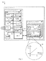
図1は、ホストデバイス(不図示)にデータ記憶装置を提供するマルチチップパッケージ(MCP)100の一例を示す。MCP100は、データを格納するためのNANDフラッシュメモリダイ103と、ホストからの読み出し及び/又は書き込みコマンドに応答してフラッシュメモリへのアクセスを容易にするフラッシュディスクコントローラ(FDC)106とを含む。いくつかの実施例において、NANDメモリダイ103は、ディープなMLCにデータを格納する。例えば、フラッシュメモリダイ103のセルは、3ビット、4ビット、5ビット、6ビット、7ビット、8ビット、9ビット、10ビット又はそれ以上の情報を保持することができるい。また、例えばMCP100は、デジタルカメラ、他の画像格納デバイス、携帯オーディオデバイス、パーソナルデジタルアシスタント(PDA)及びデジタルビデオレコーダ等の種々の携帯デバイスにおいてデータ記憶装置を提供することもできる。いくつかの実施例は、他の応用例において使用されてもよい。他の応用例には、特にデータへの迅速なアクセスが望ましい状況において、デスクトップコンピュータ、サーバ、無線ルータ又は組込みアプリケーション(例えば、自動車)が含まれてもよい。本明細書で説明する例に係る装置及び技術は、フラッシュメモリ密度を増加するため、並びに/あるいは高性能及び/又は信頼できる不揮発性データ記憶装置の動作を達成するために実現され得るものである。
FIG. 1 shows an example of a multi-chip package (MCP) 100 that provides a data storage device to a host device (not shown). The
図示する一例として、MCP100は、フラッシュメモリのセルのグループ(例えば、ページ又はブロック)における各セルに1バイト(すなわち、8ビット)の情報を格納することによりデータファイルを格納してもよい。他の例は、16ビット、32ビット、64ビット又はそれ以上の解像度を有してもよい。いくつかの実施例において、解像度は、セルのゲートにおける単一の又は複数の電子検出により判定されてもよい。他の実施例において、任意の実際のビット数の情報は、個々のフラッシュメモリセルが充電される電圧において符号化されてもよい。
As an example shown, the
FDC106は、ホストインタフェース109、プロセッサ112及びフラッシュインタフェース115を含む。FDC106は、ホストインタフェース109を介してデスクトップコンピュータ、サーバ又は携帯計算装置上のプロセッサ等のホストデバイスからコマンド及び/又はデータ(例えば、ソフトウェアコード更新データ又はユーザデータ)を受信し且つ/又はホストデバイスにデータを送信する。ホストとの通信には、例えばATA(Advanced Technology Attachment)、シリアルATA(SATA)、Block Abstracted NAND、セキュアデジタル(SD)又はマルチメディアカード(MMC)等のカスタム又は標準プロトコルを使用してもよい。いくつかの実施例において、MCP100は、ホストデバイスと同一の製品の一部としてもよい。また、他の実施例において、ホストデバイスは、プロセッサを使用する少なくとも1つの他のデバイスへの通信リンク(例えば、USB、Firewire、Bluetooth)を介してMCP100と動作可能に通信していてもよい。例えばホストは、少なくとも1つのネットワークを介して制御メッセージを送出し且つデータメッセージを送出及び受信することによりMCP100にリモートアクセスしてもよい。少なくとも1つのネットワークは、有線、無線又は光ファイバリンク、あるいはそれらの組合せを含んでもよい。そのようなネットワークは、パケットによる通信をサポートしてもよく、また、インターネット等のワイドエリアネットワーク又はローカルネットワークを含んでもよい。
The
ホストデバイス上のプロセッサは、フラッシュメモリの物理アドレスを識別するためにFDC106により処理される論理アドレス指定方式を使用して、NANDフラッシュメモリダイ103からデータを読み出してもよく且つ/又はNANDフラッシュメモリダイ103にデータを書き込んでもよい。いくつかの実施例において、ホストインタフェース109は、ATA/IDEインタフェースを使用してホストデバイスと通信するように構成されてもよい。プロセッサ112は、受信したコマンドを処理し、フラッシュインタフェース115を使用してNANDフラッシュメモリダイ103にアクセスすることができる。FDC106は、信頼性の向上、読み出し及び書き込み時間の短縮、電力効率の向上及びチップボリューム毎の容量の増加等、NANDフラッシュメモリダイ103の性能を向上するために磨耗管理機能性、ブロック管理機能性、誤り訂正機能性及び論理アドレス指定管理機能性等の機能性を提供するように構成され得る。本明細書において説明する特定の技術及び装置は、NAND及び/又はNORフラッシュメモリ、他の種類の電気的消去可能メモリ又は電気的書き込み可能メモリ、あるいはデータアクセス解像度がページ又はブロックに存在するメモリに適用可能であってもよい。
The processor on the host device may read data from the NAND flash memory die 103 and / or use a logical addressing scheme that is processed by the
図1にはNANDフラッシュメモリダイ103が1つのみ示されるが、MCP100は2つ以上のNANDフラッシュメモリダイ103を含んでもよい。いくつかの実施例は、不揮発性メモリの任意の組合せを含んでもよく、それはNANDフラッシュ、NORフラッシュ又は電気的消去可能プログラマブル読み出し専用メモリ(EEPROM)を含んでもよい。いくつかの図示する例において、MCP100は、2つ、3つ、4つ又は少なくとも8つのNANDフラッシュメモリダイ103を含むことができる。例えばMCP100は、4つのNANDフラッシュメモリダイ103とパッケージ化される(例えば、スタックに)ダイ上にフラッシュディスクコントローラ106を含んでもよい。
Although only one NAND flash memory die 103 is shown in FIG. 1, the
いくつかの実施例において、フラッシュディスクコントローラ106及びフラッシュメモリダイ103は、単一のダイ上に実現されてもよい。他の実施例において、フラッシュディスクコントローラ106の1つ以上の構成要素は、部分的又は全体的に単一のダイ又はMCP100の外部に実現されてもよい。例えば、同期ダイナミックランダムアクセスメモリ(SDRAM)151及び/又は不揮発性メモリ(NVM)154の一部又は全てがMCP100の外部に実現されてもよい。いくつかの実施例において、フラッシュディスクコントローラ106の一部又は全てがフラッシュメモリダイ103とは別にパッケージ化されてもよい。図示する一例において、NVM154、SDRAM151、ホストインタフェース109及び少なくともプロセッサ112の一部の各々はMCP100の外部に実現されてもよい。他の実施例において、フラッシュインタフェース115とフラッシュメモリダイ103との間のアナログ信号及び/又はデジタル信号は、統合パッケージに外部から転送されてもよい。
In some embodiments,
リモート又は分散送信構造(例えば、遮蔽及び/又は制御されるインピーダンス信号パス)は、少なくとも1つのフラッシュメモリダイ103に対して及び少なくとも1つのフラッシュメモリダイ103から信号を移送するために実現されてもよい。いくつかの実施例において、メモリは、不揮発性メモリの追加のパッケージをインストールすることにより拡張されてもよい。バッファリングデバイス及び/又はルーティングデバイスは、アナログ信号及び/又はデジタル信号の種々の数のメモリダイ103への配信をサポートするために使用されてもよい。更にプロセッサ112の機能は、MCP100の外部で実行されてもよい。種々の例において、プロセッサ112は、MCP100と同一の基板(例えば、プリント回路基板)の回路又は同一の製品に全体的又は部分的に実現されてもよい。プロセッサ112は、通信リンク(例えば、有線、無線、光ファイバ又はそれらの任意の組合せ)を介してMCP100と動作可能に通信する別の計算装置から実現されてもよい。
A remote or distributed transmission structure (eg, a shielded and / or controlled impedance signal path) may be implemented to transport signals to and from at least one flash memory die 103. Good. In some embodiments, the memory may be expanded by installing additional packages of non-volatile memory. Buffering devices and / or routing devices may be used to support distribution of analog and / or digital signals to various numbers of memory dies 103. Further, the functions of the
MCP100は、例えば少なくとも最大100ギガバイト以上の任意の実際的なメモリサイズを有してもよい。図示する例において、NANDフラッシュメモリダイ103は、複数のフラッシュメモリブロック118を含むように編成される。いくつかの実施例において、NANDフラッシュメモリダイ103は、数百又は数千のフラッシュメモリブロック118を含んでもよい。各フラッシュメモリブロック118は、複数のフラッシュメモリページ121を含む。図示するように、各フラッシュメモリページ121は、データ124を格納するセル及びそのデータと関連付けられる誤り訂正符号(ECC)127を格納するセルを含む。一例として、フラッシュメモリページ121は、2048バイトのデータ及び64バイトのECCデータを格納することができる。データセル124は、フラッシュディスクコントローラ106から受信される情報を格納する。ECCセル127は、データセル124に格納されるデータと関連付けられる追加の整合性メタデータ(例えば、ECCデータ)を格納する。種々の実施例において、ECCデータにより、フラッシュディスクコントローラ106はデータ中のビット誤りを検出及び/又は訂正できる。
The
図示する例において、各フラッシュメモリブロック118は1つ以上の参照セル130a、130b、130cを更に含む。いくつかの実施例において、FDC106は参照セル130a、130b、130cの電圧を監視して、セル124、127において電圧の低下度又はドリフトの程度を推定するように構成される。各ブロック118において、参照セル130aはブロック118の開始部分に位置付けられ、参照セル130bはブロック118の終了部分に位置付けられるようしてもよい。また、各フラッシュメモリページ121は参照セル130cを含んでもよい。いくつかの実施例において、より多くの参照セル又はより少ない参照セルがメモリ103のページ、ブロック及びダイにわたり任意のパターンで分布され、セル124、127の予想される性能を判定するようにしてもよい。
In the illustrated example, each flash memory block 118 further includes one or
いくつかの実施例において、参照セルは、特定の関心データセルの使用レベルを表す読み出し/書き込み使用レベルを体験するセル中に又はセルの周囲に位置付けられる。補償方法は、非参照セルを他の非参照セルと比較することに基づいてなされる。例えば同一のページ又はブロックの複数のセルの電圧が相対的に低い場合、補償は、読み出し誤りが大きく低減されるように測定値に従って閾値(例えば、セル中の異なる値レベル間の電圧閾値)を調整して小さくすることを含んでもよい。また、他の例は、参照セルの検出電圧に基づく補正関数を判定することを含み、その補正関数は、検出電圧をメモリセルにより表されるデジタルデータ値に変換する前に、その検出電圧を調整する。 In some embodiments, the reference cell is positioned in or around a cell that experiences a read / write usage level that represents the usage level of a particular data cell of interest. The compensation method is based on comparing non-reference cells with other non-reference cells. For example, if the voltages of multiple cells on the same page or block are relatively low, the compensation will set a threshold (eg, a voltage threshold between different value levels in the cell) according to the measurement so that read errors are greatly reduced. It may include adjusting to make it smaller. Another example also includes determining a correction function based on the detection voltage of the reference cell, which correction function converts the detection voltage to a digital data value represented by the memory cell before converting the detection voltage. adjust.
いくつかの実施例において、メモリセルは、検出された電圧低下に対して補正を行なうために複数のセルに追加の電荷を印加することによりリフレッシュされる。例えば、1つ以上の参照セルの電圧レベルがある電圧ドリフトの閾値量を超えることを示す場合、その参照セルに関連するページ又はブロックのメモリセルは、追加の電荷を印加することにより調整され得る。あるいは格納データに従ってセルを適切な電圧レベルに復元するために書き換えられてもよい。そのような調整は、参照セルの電圧ドリフトを検出した直後に実行されるか又は後の保守動作の一部として実行される。いくつかの実施例において、追加の電荷が印加されてもよく、あるいはメモリセルは検出された参照セル電圧と目標参照セル電圧との差分に基づいて書き換えられてもよい。その差分は、参照セル及び対応するデータセルの双方に対する電圧ドリフト又は低下の大よその量を示すと仮定されてもよい。 In some embodiments, the memory cell is refreshed by applying additional charge to the plurality of cells to compensate for the detected voltage drop. For example, if the voltage level of one or more reference cells indicates that it exceeds a threshold amount of voltage drift, the page or block of memory cells associated with that reference cell can be adjusted by applying additional charge. . Alternatively, the cell may be rewritten to restore the cell to an appropriate voltage level according to the stored data. Such adjustment is performed immediately after detecting the voltage drift of the reference cell or as part of a subsequent maintenance operation. In some embodiments, additional charge may be applied, or the memory cell may be rewritten based on the difference between the detected reference cell voltage and the target reference cell voltage. The difference may be assumed to indicate an approximate amount of voltage drift or drop for both the reference cell and the corresponding data cell.
他の実施例において、追加の電荷の印加又はメモリセルの書き換えは、全てのセルを読み出し、閾値への任意の必要な調整を実行し(例えば、参照セル電圧に基づく補正関数を使用し且つ/又は本明細書において説明する他の技術を使用して)、格納されるデータを取得するために検出データに対して誤り訂正を実行することにより実行されてもよい。その後データは、識別された電圧のドリフト又は低下に対して種々のメモリセルを補正するのに必要とされる追加の電荷量又は適切な電圧レベルを判定するために使用される。いくつかの実施例によれば、印加される追加の電荷量は、検出電圧をデジタルデータ値に変換する前に検出電圧を調整するために使用された補正関数と同一の又はそれに類似する補正関数に基づいて判定される。 In other embodiments, the application of additional charge or rewriting of the memory cells reads all cells and performs any necessary adjustments to the threshold (eg, using a correction function based on the reference cell voltage and / or (Or using other techniques described herein) may be performed by performing error correction on the detected data to obtain stored data. The data is then used to determine the amount of additional charge or appropriate voltage level needed to correct the various memory cells for the identified voltage drift or drop. According to some embodiments, the additional charge applied is a correction function that is the same as or similar to the correction function used to adjust the detection voltage before converting the detection voltage to a digital data value. It is determined based on.
いくつかの実施例において、フラッシュメモリのセルは適応可能に再割り当てされてもよい。例えば参照セルは、読み出し又は書き込み使用情報、温度、製品年齢、供給電圧(例えば、低バッテリ、交流電源)及び/又は検出誤りレベルに応答して適宜追加、除去、再配置及び/又は再分布されてもよい。メモリのある特定のブロック又はページにおける誤りが少ない場合、ECCセル127及び/又は参照セル130として割り当てられるセルをより少なくしてもよく、それによりデータセル124は更に多くすることができる。参照、データ及びECC機能に対するセルの相対的な割り当て、並びに個々のセルの解像度は、現在の動作条件に基づき且つ/又は所定の条件に従って動的に調整されてもよい。例えば、解像度は誤り率に基づいて調整されてもよく、ページ毎のECCセル数は誤り率、並びに読み出し及び書き込み履歴情報に基づいてもよく、参照セルの場所及び分布は誤り率及び製品年齢に基づいてもよい。この例は、単にコントローラ106及びフラッシュメモリダイが種々の基準に従って動的に調整されてもよいことを示す。他の基準は、データの重要度、電源の可用性(例えば、交流電源、バッテリ電源)、並びにメモリサイズ、速度性能及びデータ整合性を最大限にする相対的な重要さに関する規定の基準を含んでもよい。例えば、非常に多くのソフトウェア補正を必要とする高いセル解像度を維持することにより、アクセス時間は更に長くなる可能性がある。基準は、応用例の要求に従ってユーザ、製品製造業者又はソフトウェアにより適応されてもよい。
In some embodiments, the flash memory cells may be adaptively reallocated. For example, reference cells may be added, removed, rearranged and / or redistributed as appropriate in response to read or write usage information, temperature, product age, supply voltage (eg, low battery, AC power) and / or detection error level. May be. If there are fewer errors in a particular block or page of memory, fewer cells may be allocated as
いくつかの実施形態において、非常に多くのソフトウェア補正を必要とするデータは、時間の経過に関連する電荷の変動を補正するために又は劣化し始めたメモリセルのページを補正するために保守動作において書き換えられてもよい。1つ以上のメモリセルの解像度を変更する場合、データはメモリセルの異なるページに書き込まれ、同一の又は異なる解像度で書き込まれる。いくつかの実施例において、メモリセルの元のページはより低い解像度にダウングレードされる。これは、メモリセルが経時変化により劣化するにつれて必要とされる場合が多い。データの書き換えが識別された電圧ドリフト又は低下の結果として実行される場合、メモリセルの同一の又は異なるページ又はブロックにデータを書き込むことができる。 In some embodiments, data that requires a large number of software corrections is a maintenance operation to correct charge variations associated with time or to correct pages of memory cells that have begun to degrade. May be rewritten. When changing the resolution of one or more memory cells, data is written to different pages of the memory cell and written at the same or different resolution. In some embodiments, the original page of memory cells is downgraded to a lower resolution. This is often required as the memory cell degrades over time. Data can be written to the same or different pages or blocks of memory cells if data rewriting is performed as a result of identified voltage drift or degradation.
フラッシュインタフェース115は、フラッシュメモリダイ103に対する直接制御、ハンドシェーク及びデータ転送アクセスを提供する。フラッシュインタフェース115は、制御インタフェース133及びアナログインタフェース136を含む。いくつかの実施例において、制御インタフェース133は、制御、アドレス及びデータ信号をフラッシュメモリダイ103に送出することができる。コマンド及びメモリアドレスは、デジタル信号又はアナログ信号で送信され得る。更にフラッシュディスクコントローラ106は、フラッシュメモリダイ103からアナログ信号を受信できる。フラッシュディスクコントローラ106は、フラッシュメモリダイ103上のフラッシュメモリ論理とインタフェースするためのプロセッサを含んでもよく、フラッシュダイ上のフラッシュメモリ論理とインタフェースするためのこのプロセッサは、フラッシュインタフェース115に組み込まれてもよい。
The flash interface 115 provides direct control, handshaking and data transfer access to the flash memory die 103. The flash interface 115 includes a
フラッシュメモリダイ103は、読み出しコマンドに応答して、個々のデータセル124に格納されたデータを表すセル電圧を出力してもよい。フラッシュディスクコントローラ106は、フラッシュメモリダイ103上の各メモリセルから出力されたアナログ電圧信号を受信できる。それらのアナログセル電圧又はアナログ電圧信号は、FDC106のアナログインタフェース136に送信される。いくつかの実施例において、フラッシュインタフェース115は、制御インタフェース133とは別個のデータバス及びフラッシュメモリダイ103と通信するためのアナログインタフェース136を更に含み得る。
The flash memory die 103 may output cell voltages representing data stored in the individual data cells 124 in response to the read command. The
アナログインタフェース136は、アナログフロントエンド(アナログFE)139及びアナログ/デジタル変換器(ADC)142を含む。アナログFE139は、アナログ信号を受信すると、例えばオフセット、補正レベルシフト、利得、バッファリング、フィルタリング又は制御インピーダンスを提供して反射を最小限にするために、必要に応じて信号を適応させてもよい。アナログFEは、高いインピーダンス入力を提供してフラッシュメモリセルの負荷を最小限にしてもよいし、また低いインピーダンス出力を提供して、ADC142の入力に結合されるサンプルホールド回路又はトラックホールド回路を駆動してもよい。いくつかの実施例において、アナログFE139は、1つ以上のフラッシュメモリダイからの複数のアナログ出力線のうち1つを選択するためにアナログマルチプレクサ(不図示)を更に含む。
The analog interface 136 includes an analog front end (analog FE) 139 and an analog / digital converter (ADC) 142. Upon receiving an analog signal, the
ADC142は、データセル124、127の電圧の対応するデジタルデータ値表現を判定するためにアナログ値を処理する。ADC142は、適応されたアナログ信号を受信し、アナログ信号をアナログ電圧のデジタル表現に変換する。ADC142(又はADCのプロセッサ)は、例えばマッピング関数に基づいてメモリセルに格納された電圧により表されるデジタルデータ値にそのデジタル表現を変換する。プロセッサ112は、デジタル表現をデジタルデータ値に変換するために更に使用される。アナログ電圧のデジタル表現は、各々が特定のデジタルデータ値を表す複数のアナログ電圧レベルをADC142又はプロセッサが区別できるように十分な情報を含み得る。デジタル表現は、デジタルデータ値より多くのビット数のデータを含んでもよい。いくつかの実施例において、ADC142は、フラッシュディスクコントローラ106に含まれるのではなく、フラッシュメモリダイ103に組み込まれる。そのような場合、フラッシュインタフェース115は、フラッシュメモリダイ103からセル電圧のデジタル表現又はデジタルデータ値を受信することになる。
The
マッピング関数145の一例を示す。マッピング関数145に基づいて、ADC142又はプロセッサ112は、アナログセル電圧をデジタル表現及び/又はデジタルデータ値に変換することができる。例えば、アナログ電圧をデジタル表現及び/又はデジタルデータ値にマップするために使用される一連のアナログ電圧閾値が存在してもよい。同様に、マッピング関数145は、アナログ電圧のデジタル表現のデジタルデータ値への変換を更に示してもよい。例えば、アナログ電圧の1つ以上のデジタル表現を、特定のデジタルデータ値にマップしてもよく、各デジタルデータ値は1つ以上のデジタル表現の対応する別個の集合を有する。
An example of the
いくつかの実施例において、ADC142又はプロセッサ112は、マッピング関数145を変更するパラメータを受信するように構成される。例えばFDC106は、現在の温度、供給電圧、ページデータの読み出し及び書き込み回数、並びに/あるいは参照セル130a、130b及び/又は130cの電圧に基づいてマッピング関数を適応させる。いくつかの実施例において、マッピング関数に対する適応は、隣接するデータセル124、ECCセル127及び/又は他のセルの電圧特性に基づく。セル電圧とデジタルデータ値とのマッピング145については、図2A及び図2Bを参照して更に詳細に説明する。また、いくつかの実施例において、ADC142又はプロセッサは、受信したアナログ信号又はアナログ信号のデジタル表現に対する代替値を検索するための代替値コマンドに応答可能に動作する。代替値コマンドの実施例については、図6A〜図6Cを参照して更に詳細に説明される。
In some embodiments, the
フラッシュディスクコントローラ106は、ECCエンジン148を更に含む。種々の実施例において、ECCエンジン148は、ECCセル127を使用してハードウェア及び/又はソフトウェア誤り検査訂正を実行する。また、いくつかの実施例において、ECCエンジン148は、状態遷移機械を使用するデータ回復を提供する。例えばECCエンジン148は、データのページの誤りビット数を検出するように構成される。ECCエンジン148は、使用されるECCアルゴリズムを判定してもよい。一例としてECCエンジン148は、まず、例えばハミング符号又はリードソロモン符号を使用してハードウェアECCアルゴリズムを試行するように構成され得る。そして、ハードウェアECCアルゴリズムがデータのページの回復時に失敗した場合、ソフトウェアECC訂正が試行されてる用に構成してもよい。ハードウェアECC,ソフトウェアECC及び他の技術を組み合わせて使用することを示す方法の一例については、図5を参照して後に説明する。いくつかの実施例において、ECCエンジン148は、データのページのサイズの最大少なくとも約10%以上に対して誤り訂正を提供することができる。また、いくつかの例において、プロセッサが使用するECCアルゴリズムを判定するようにしてもよい。
The
いくつかの実施例において、ECCアルゴリズムが所定の数又は所定の割合より多い誤りを含むデータを回復するために使用される場合、プロセッサ112は、フラッシュメモリページに格納されたデータを書き換えるか又はリフレッシュする。他の実施例において、プロセッサ112は、保守ログにそのような誤りを含んでいたデータの物理的及び/又は論理的な場所を記録する。プロセッサ112は、保守動作中にそのデータを書き換えるか又はリフレッシュする(図9を参照)。保守動作は、ホストデバイスが所定の電力条件下で動作している時に実行されるようにしてもよいし、プロセッサ112が所定量の余分な帯域幅を有する時に実行されるようにしてもよいし、且つ/又はスケジュールされた間隔で実行されるようにしてもよい。
In some embodiments, if the ECC algorithm is used to recover data that contains a predetermined number or more than a predetermined percentage of errors, the
フラッシュディスクコントローラ(FDC)106は、ダイナミックランダムアクセスメモリ(DRAM)を含んでもよい。この例のフラッシュディスクコントローラ106は、同期ダイナミックランダムアクセスメモリ(SDRAM)151を更に含む。例えばSDRAM151は、SDR(single data rate)SDRAMでもよいし、或いはDDR(double data rate)SDRAMでもよい。いくつかの実施例において、例えばFDC106は、ホストデバイスに対する出力データ及びデータのページに対する代替デジタル値等の一時データを格納するためにSDRAM151を高速で高密度なバッファとして使用され得る。また、FDC106は、DRAM等の他の種類のRAMを更に含んでもよい。一例として、FDC106はNANDフラッシュメモリダイ103からアナログデータを受信してもよい。
The flash disk controller (FDC) 106 may include dynamic random access memory (DRAM). The
FDC106は、場合によっては1つ以上のセルに対して代替デジタルデータ値を含むデジタルデータに、検出したアナログ電圧を変換してもよい。ECCエンジン148は、デジタルデータを検査及び訂正し、可能性としては各フラッシュメモリページ121上のセルに対するデータ値及び代替データ値の複数の異なる組合せを検査する。誤り訂正が成功した場合、プロセッサ112は、デジタルデータをSDRAM151のホスト出力バッファに格納してもよい。いくつかの実施例において、ホストデバイスは、ホスト出力バッファからデータを検索する。あるいは、フラッシュディスクコントローラ106はデータをホスト出力バッファからホストデバイスに転送してもよい。SDRAM151又は他のキャッシュメモリは、フラッシュメモリダイ103に書き込まれるデータを格納するために更に使用されてもよい。
The
FDC106は、不揮発性メモリ(NVM)154を更に含む。この例において、NVM154は、磨耗管理ソフトウェアコード157、ブロック管理ソフトウェアコード160、論理アドレス指定ソフトウェアコード163及びセル解像度レジスタ166を含み、それら各々は、プロセッサ112により実行された時に特定の動作を実行する命令(又はフラッシュメモリ中の命令に対するポインタ)を含む。いくつかの実施例において、NVM154はNANDフラッシュメモリダイ103とは別個であってもよい。例えばNVM154は、NORフラッシュメモリであってもよく又は別のNANDフラッシュメモリであってもよい。他の実施例において、NVM154はNANDフラッシュメモリダイ103の1つ以上のページであってもよい。他の実施例において、NVM154はNANDフラッシュメモリダイ103に格納されたデータに対するポインタ又は記憶場所を格納する。いくつかの実施例において、プロセッサ112は、磨耗管理ソフトウェアコード157、ブロック管理ソフトウェアコード160及び論理アドレス指定ソフトウェアコード163を実行して、MCP100の効率、性能及び/又は信頼性を向上する。
The
プロセッサ112は、磨耗管理ソフトウェアコード157を使用してMCP100のページ121、ブロック118又はダイ103の磨耗を管理するように構成される。例えば磨耗管理ソフトウェアコード157は、プロセッサ112により実行された時に最も頻繁に使用されるメモリページのデータを使用頻度の少ないメモリページに交換するための負荷均一化動作を含む動作を実行する命令を含んでもよい。交換動作は、論理アドレス指定ソフトウェアコード163の更新を更に含んでもよい。
The
磨耗管理ソフトウェアコード157は、保守動作中に起動され得る。いくつかの実施例において、各読み出し動作の物理アドレス及び/又は論理アドレスは、保守ログに記録される。更に、各書き込み動作が保守ログに記録されてもよい。磨耗管理ソフトウェアコード157は、メモリセルのページ間で格納されたデータを再配置する方法を判定するために所定の閾値を使用してもよい。例えばそれら閾値は、1週間又は1ヶ月の間にメモリセルのページの100回又は1,000回の読み出し、といったものが挙げられる。他の実施例において、閾値は読み出し動作の合計回数の割合に基づいてもよく、あるいは時間毎のページ毎の読み出し平均回数からの偏差に基づいてもよい。保守動作の一例については、図9により後述する。
The wear
ブロック管理ソフトウェアコード160は、フラッシュメモリダイ103の不良ブロックを管理するためのコードを含む。例えばブロック管理ソフトウェアコード160は、フラッシュメモリブロック118に関する履歴誤り情報を含み得る。いくつかの実施例において、誤り情報は各フラッシュメモリページのセル解像度を維持するために使用される。ブロック管理ソフトウェアコードの一例については、後に、図8A及び図8Bを参照して更に詳細に説明する。
The block
フラッシュメモリダイ103中の低下した解像度(セル解像度レジスタ166において更新される)を有する不良ブロック又は不良ページの集合を対にし、論理アドレス指定の目的で、初期のより高い解像度を有するメモリセルの単一のブロック又は単一のページの等価物としてその不良ブロック又は不良ページの集合を処理するようにする(論理アドレス指定ソフトウェアコード163及び/又はセル解像度レジスタ166において更新される可能性が高い)ために、ブロック管理ソフトウェアコード160は使用されてもよい。ここで、ブロック管理ソフトウェアコード160は、おそらくは、論理アドレス指定ソフトウェアコード163及び/又はセル解像度レジスタ166と共に使用される。また、ブロック管理ソフトウェアコード157は、保守動作中に起動され得る。保守動作の一例については図9により後述する。
A pair of bad blocks or bad pages having a reduced resolution (updated in the cell resolution register 166) in the flash memory die 103 is paired, and for the purpose of logical addressing, an initial higher resolution memory cell unit. To treat the bad block or set of bad pages as a block or single page equivalent (possibly updated in logical addressing software code 163 and / or cell resolution register 166) In addition, block
論理アドレス指定ソフトウェアコード163は、ホストコマンドの論理アドレスをNANDフラッシュメモリダイ103の物理アドレスに変換するためのコードを含み得る。いくつかの例において、論理ページはNANDフラッシュメモリダイ103の複数の物理メモリページと関連付けられる。論理アドレス指定ソフトウェアコード163は、NVM154の論理アドレステーブルの変換及び更新を管理する。一例において、ページが10ビット解像度から8ビット解像度にダウングレードされるか又は論理ブロックアドレスから異なる物理ページアドレスへのマッピングが磨耗管理の目的で変更されると、論理アドレス指定ソフトウェアコード163は、ホストからの論理ブロックアドレスと物理ページアドレスとのリンクを動的に維持するように構成される。例えばアドレスの中間形式は、論理アドレスと物理アドレスとの変換の処理中に生成され得る。中間アドレス形式は、種々の不揮発性メモリ動作を実行するために生成、処理、格納、使用及び/又は操作され得る。論理アドレス指定ソフトウェアコードの一例については、図10を参照して更に詳細に後述する。
The logical addressing software code 163 may include code for converting the logical address of the host command to the physical address of the NAND flash memory die 103. In some examples, the logical page is associated with multiple physical memory pages of NAND flash memory die 103. The logical addressing software code 163 manages the conversion and update of the logical address table of the
セル解像度レジスタ166は、セル解像度に関する情報を各フラッシュメモリページ121に格納する。例えばNANDフラッシュメモリダイ103は、8ビットMLCフラッシュメモリである。いくつかの実施例において、フラッシュメモリブロック118の一部は、種々の条件に応じてダウングレード又はアップグレードされ得る。そのような条件の例は、誤り性能、温度、電圧条件、個々のセルの読み出し又は書き込み周期の回数、セルのグループ、ページ、隣接する場所にあるセル、参照セル、同等の読み出し及び/又は書き込み使用履歴を有するセル、あるいはデバイスの経時変化等の他の因子を含む。それら条件の一部又は全てに関する情報は、データ記憶装置に格納されてもよく、あるいは格納された1ビット以上の他の情報から判定又は推定されてもよい。一例において、格納された情報は、メモリダイ103の少なくとも一部のセルに対する使用レベルを表す履歴読み出し/書き込み使用データを含んでもよい。プロセッサ112は、ダウングレードされたメモリページのセル解像度を例えば4ビットに低減するようにセル解像度レジスタ166を更新してもよいため、フラッシュメモリページ121はより小さなメモリサイズで使用可能である。他の実施例において、セル解像度レジスタ166は、各フラッシュメモリブロック118に対するセル解像度を更に格納してもよい。
The cell resolution register 166 stores information on cell resolution in each flash memory page 121. For example, the NAND flash memory die 103 is an 8-bit MLC flash memory. In some embodiments, a portion of the flash memory block 118 may be downgraded or upgraded depending on various conditions. Examples of such conditions are error performance, temperature, voltage conditions, number of individual cell read or write cycles, cell groups, pages, adjacent cells, reference cells, equivalent read and / or write. Includes other factors such as cells with usage history or device aging. Information about some or all of these conditions may be stored in a data storage device, or may be determined or estimated from other information stored in one or more bits. In one example, the stored information may include historical read / write usage data that represents a usage level for at least some cells of the memory die 103. The
いくつかの実施例において、セル解像度レジスタ166は、データをホストデバイスからMCP100のメモリセルに転送する前に調整されて単一ビットの解像度又は別の少ないビット数の低解像度にされる。この処理については、図7Bを参照して更に詳細に後述する。各メモリセルを充電するのに必要な精度はより低くなるため、データを転送する前にセル解像度レジスタ166を低減することにより、更に高速なデータ転送速度が可能になる。その後、転送されたデータはより高い解像度でメモリセルに書き換えられてもよい。いくつかの実施例において、転送されたデータは、保守動作中に(例えば、十分な処理リソースが利用可能であり且つ書き換えが他の読み出し又は書き込み動作を妨害しない時に後で)より高い解像度で書き換えられてもよい。いくつかの実施例において、低いセル解像度のデータ転送が保守ログに記録される。
In some embodiments, the cell resolution register 166 is adjusted to a single bit resolution or another low bit number low resolution prior to transferring data from the host device to the memory cells of the
いくつかの実施例において、論理アドレス指定ソフトウェアコード163、解像度レジスタ166及び/又はブロック管理ソフトウェアコード160はダウングレードされたメモリページ(又はダウングレードされたメモリブロック)をグループ化し、論理アドレス指定の目的でそのグループをダウングレードされていない単一のメモリページ(又はブロック)として処理する。ダウングレードされたメモリページのグループのメモリページは隣接するメモリページである必要はない。ダウングレードされたメモリページのグループは、異なるブロック及び異なるメモリダイのメモリページを含むことができる。いくつかの実施例において、ダウングレードされたメモリページ又はブロックのグループのダウングレードされた各メモリページ又はブロックは、そのページ又はブロックに関連する誤り条件に応じてダウングレードされる。
In some embodiments, the logical addressing software code 163, the resolution register 166, and / or the block
図2A及び図2Bは、メモリセルに格納されたデジタルデータ値とセル電圧とのマッピングを一括して示す。図2Aに示すように、8ビットメモリセルのデジタルデータ値分布200の例を示す。8ビットメモリセルは、256個の可能なデジタルデータ値を含み、4ビットメモリセルは16個の可能なデータ値を含む。可能なデータ値の数は2n(nはビット数である)に等しいが、可能なデジタルデータ値の数は可能なデジタルデータ値のnビット数に対応する必要はない。各メモリセルは1より大きい整数の数の可能なデジタルデータ値を有することができる。例えばメモリセルの中には10個の可能なデータ値を有することができるものもある。デジタル値分布200は、各デジタルデータ値の電圧分布を表すデジタル値分布曲線205〜210を含む。各デジタル値分布曲線(例えば、205〜210)は、可能な各デジタルデータ値と関連付けられる電圧レベルに対応するデジタル電圧値の範囲を表す。
2A and 2B collectively show mapping between digital data values stored in memory cells and cell voltages. As shown in FIG. 2A, an example of a digital
書き込み動作中、各メモリセルは、可能なデジタルデータ値のうちの1つから選択されたデジタルデータ値に対応するアナログ電圧になるまで電荷を受け取る。一般にこの対応する電圧は、所望のデジタルデータ値に対する分布曲線205〜210内に入る。この対応する電圧は、デジタルデータ値に対応する目標電圧であってもよい。例えばセル電圧が分布207内に入る場合、セルに格納されるデジタル値は02Hとなる。読み出し動作中、アナログ電圧信号は各セルから検出される。ADC136は、アナログ電圧信号をアナログ電圧信号のデジタル表現に変換する。このデジタル表現は、少なくとも1つのデジタル値分布曲線と比較されて、読み出したメモリセルに格納されたアナログ電圧により表されるデジタルデータ値を判定する。
During a write operation, each memory cell receives charge until an analog voltage corresponding to a digital data value selected from one of the possible digital data values is reached. In general, this corresponding voltage falls within the distribution curve 205-210 for the desired digital data value. This corresponding voltage may be a target voltage corresponding to the digital data value. For example, when the cell voltage falls within the
デジタルデータ値分布200は、デジタルデータ値分布曲線205〜210の間のグレー領域215を含む。いくつかの実施例において、ADC142がグレー領域215のうち1つの領域内にあるアナログ電圧信号を検出するか又はセル電圧を受信する場合、例えばADC142は、セル電圧を最近接するデジタルデータ値に変換する。例えばADC142が電圧レベル220に非常に近接するセル電圧を受信する場合、ADC142は、セル電圧を最近接するデジタルデータ値、すなわちFEHに変換する。いくつかの実施例において、FDC106は、いくつかのパラメータに基づいて最近接する値以外の代替値に変換するようにADC142に命令する代替値コマンドを更に含み得る。
The digital
いくつかの実施例において、FDC106は、データ値のページ又はブロックを変換しようとする誤り訂正処理において最近接するデジタルデータ値及び1つ以上の代替値を使用することができる。更にFDC106は、デジタルデータ値分布曲線205〜210又はグレー領域215内のセル電圧の場所に基づいて特定のセル電圧又は対応するデータ値に不確実性を割り当ててもよい。割り当てられた不確実性は、データ値のページ又はブロックを変換しようとするアルゴリズムにより使用され得る。それらパラメータのいくつかの例としては、温度、セルに対する読み出しの回数、セルに対する書き込みの回数、供給電圧及び参照セル130a、130b、130cの電圧のうち1つ以上が含まれ得る。いくつかの例において、セル電圧は最低セル電圧(Vmin)を下回るまで低下してもよい。FDC106は、受信したセル電圧にオフセットを加算することにより補正を行なってもよい。このオフセットは、アナログFE139により加算されてもよく、あるいはADC142又はプロセッサ112によりデジタルに加算されてもよい。
In some embodiments, the
いくつかの実施例において、FDC106は、デジタルデータ値分布200を変更することによりグレー領域215の幅及び場所を動的に調整してもよい。例えばFDC106は、1つ以上の参照セル電圧、メモリセルの使用及びNVM154に事前にロードされてもよい他のヒューリスティック等のパラメータに基づいてグレー領域215を調整する保守ソフトウェアコードを含んでもよい。そのような保守ソフトウェアコードは、セル解像度レジスタ166の更新を実行してもよい。例えば各ダイ103、アナログインタフェース135及び/又はMCP100は、製造時間及び線形化テーブルにおいて特徴付けられてもよく、あるいは補正係数又は他の補正調整は、MCP100の不揮発性メモリに格納されてもよい。場合によっては、最大電圧レベル(Vmax)、最小電圧レベル(Vmin)及びデジタル値分布曲線205〜210は、使用寿命の間のセルの実験テストに基づいて調整及び/又は最分布されてもよい。
In some embodiments, the
図2Bに示すように、セル電圧対デジタル値のグラフ250が示される。グラフ250は、ADC142がアナログ電圧をデジタル値に変換するのに使用する理想的な電圧特性255を含む。いくつかの例において、データセル124は、例えば温度、セルの経時変化、チャージポンプ又は供給電圧許容差、ADC136の非線形性、メモリセルにおける検出誤り、並びに/あるいはセルの読み出し及び書き込み回数のヒューリスティックによる理想的でない電圧特性260、265に従ってデジタル値を格納する。FDC106は、理想的な特性255に近付くように電圧特性260、265を種々の方法で補償するように構成される。以下、図3A、図3B、図4、図5、図6A〜図6Cを参照して、補償方法の例を説明する。
As shown in FIG. 2B, a
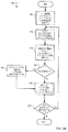
図3A及び図3Bは、NANDフラッシュメモリからデータのページを読み出すための処理350及び300の例を示すフローチャートである。処理350及び300は、プロセッサ112により実行され得る動作を含む。なお、いくつかの実施例において、処理350及び300は、ADC142と組み合わされ得る他の処理及び/又は制御素子により実行、補足又は強化されてもよい。例えば、コントローラ又は補償器は、処理350及び300の動作の一部又は全てを実行するアナログインタフェース136に存在してもよい。
3A and 3B are flowcharts illustrating examples of
図3Aは、多値メモリセルからの検出電圧レベルをデジタルデータ値に変換する処理を示す。処理350は、多値メモリセルからアナログ電圧レベルを検出することから開始する(ステップ355)。例えばこの電圧は、アナログインタフェース136により検出され得る。アナログインタフェース136は、フラッシュメモリダイ103からアナログ信号を受信するように動作可能な入力部を含んで構成され得る。フラッシュディスクコントローラ106は、入力部が受信するアナログ信号の送信元のメモリセルを選択するための制御モジュールを更に含んでもよい。ステップ360において、アナログ電圧信号は、検出されたアナログ電圧のデジタル表現に変換される。この変換は、ADC142により実行され得る。デジタル表現は、デジタルデータ値を表す複数の可能な電圧レベルのうちメモリセルにより格納されたアナログ電圧のレベルをADC142又はプロセッサ112が区別できるように十分なデータを有し得る。これは、デジタル表現がメモリセルに格納された電圧により表されるデジタルデータ値より多くのビット数のデータを含むようにすることにより達成され得る。
FIG. 3A shows a process for converting the detected voltage level from the multi-level memory cell into a digital data value.
図2Aは、この概念を示すことを助長する。可能なアナログセル電圧の範囲は、各々がアナログセル電圧のデジタル表現に対応する複数のセグメント(例えば、電圧レベル220により表されるような)に分離されてもよい。各デジタル値分布曲線205〜210及び各グレー領域215はそのようなセグメントの複数を含んでもよく、例えば、セル電圧がデジタル値分布曲線205〜210又はグレー領域215内のどこにあるかに関する追加の情報を提供でき且つデジタル値分布曲線205〜210より高い解像度を有するデジタル表現の使用を可能にする。
FIG. 2A helps illustrate this concept. The range of possible analog cell voltages may be separated into multiple segments (eg, as represented by voltage level 220), each corresponding to a digital representation of the analog cell voltage. Each digital value distribution curve 205-210 and each
ステップ365において、デジタル表現は、デジタルデータ値分布に基づいてデジタルデータ値に変換される。デジタルデータ値分布は、セル解像度レジスタ166に格納されてもよく、例えば、図2Aに示すデジタルデータ値分布200であってもよい。ステップ335において、プロセッサ又はコントローラは、読み出すメモリセルが更に存在するかを判定する。存在する場合、ステップ355に戻る。存在しない場合、処理350は終了する。
In
図3Bは、識別されたデジタルデータ値を格納し且つ不確実なデジタルデータ値の場所に印をつける処理を更に詳細に示す。例えばプロセッサ112がNANDフラッシュメモリダイ103からデータのページを検索するためのコマンドを受信した時、処理300は開始する。ステップ305において、プロセッサ112はセル解像度レジスタ166からページに対するセル解像度情報を検索する。その後、ステップ310において、プロセッサ112は、データセルに対するデジタル出力値をADC142から受信する。データセルに対するデジタル出力値は、データセルから検出された電圧のデジタル表現である。ADC142は、ステップ315において、格納された閾値に基づいて受信デジタルデータ値を判定する。いくつかの実施例において、プロセッサ112は、使用される閾値の集合を判定するためにセル解像度レジスタ166の情報を使用してもよい。それらの閾値は、図2Aに関して上述したデジタル値分布曲線205〜210に関連してもよい。例えばプロセッサ112は、8ビットセルに対して閾値の1つの集合を使用し、2ビットセルに対して閾値の別の集合を使用してもよい。場合によっては、プロセッサ112は、1つの8ビットセルに対して閾値の1つの集合を使用し、異なる8ビットセルに対して閾値の別の集合を使用してもよい。閾値の各集合は、可能なデジタルデータ値分布に対応してもよく、可能なデジタルデータ値に対応するアナログ電圧のデジタル表現の範囲を構成してもよい。
FIG. 3B shows in more detail the process of storing the identified digital data value and marking the location of the uncertain digital data value. For example, when the
ステップ320において、プロセッサ112は、受信アナログ電圧値に対するデジタルデータ値が不確実であるかを判定する。いくつかの実施例において、セル電圧がデジタル値分布200のグレー領域215にある場合、又は、セル電圧がデジタル値分布曲線205〜210とグレー領域215との境界近くにある場合、プロセッサ112は、デジタルデータ値が不確実であると判定する。また、いくつかの実施例において、種々のレベルの不確実性は、セル電圧がデジタル値分布200内のどこにあるかに依存して割り当てられる(例えば、より高い電圧はより大きい不確実性を有する傾向があるとしてもよく、且つ/又は、不確実性はグレー領域215の中間に近いセル電圧程高くなるとしてもよい)。ステップ320において、受信デジタル値が不確実でないとプロセッサ112が判定した場合、プロセッサ112は、ステップ325においてホスト出力バッファに受信デジタル値を格納する。一方、ステップ320において、受信デジタル値が不確実であるとプロセッサ112が判定した場合、プロセッサ112は、ステップ330においてマスクテーブルの不確実なデジタル値の場所に印をつけ、その後、ステップ325を実行する。いくつかの実施例によれば、1つ以上の代替値が、正確な値(例えば、不確実な値又は代替値のうちの1つ)を得る際に後で使用するために格納される。
In
プロセッサ112が受信デジタル値を格納した後、ステップ335において、プロセッサ112は読み出すセルが更に存在するかを判定する。例えばプロセッサ112は、メモリページの最後に到達したかを検査してもよい。読み出すセルが更に存在する場合、ステップ310に戻る。読み出すセルがそれ以上存在しない場合、処理300は終了する。いくつかの実施例において、更に処理は、メモリセルのページ又はブロックと関連付けられる不確実なデータ値の数を保守ログに記録する。他の実施例において、不確実なデータ値の数が所定の閾値を超える場合、処理はメモリセルのページ及び/又はブロックの物理的及び/又は論理的な場所を記録する。
After the
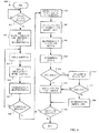
図4は、デジタル値へのセル電圧のマッピングを調整する補正関数を使用してNANDフラッシュメモリダイ103等のMLCフラッシュメモリからデータのページを読み出すための処理400の一例を示すフローチャートである。例えば処理400は、プロセッサ112により実行される。処理400は、読み出しコマンドを受信したかをプロセッサ112が判定するステップ405において開始する。例えばFDC106は、ホストインタフェース109を介してホストデバイスから読み出しコマンドを受信し得る。ステップ405において、読み出しコマンドを受信していないとプロセッサ112が判定した場合、ステップ405が繰り返される。
FIG. 4 is a flowchart illustrating an example of a
ステップ405において、読み出しコマンドが受信されたとプロセッサ112が判定した場合、ステップ410において、プロセッサ112は、温度、メモリページにおける読み出し又は書き込み回数、供給電圧、並びに/あるいは、NANDフラッシュメモリダイ103の他の動作条件に基づいて補正関数を更新する。いくつかの実施例において、ADC142又はアナログインタフェース136は、セル電圧がデジタル値に変換される前にアナログフロントエンド139において測定セル電圧を調整するために補正関数を使用する。他の実施例において、プロセッサ112はマッピング関数の閾値を調整するために補正関数を使用し、それによって、ADC142はアナログ電圧を調整されたデジタル値に変換することを可能としても良い。補正関数は、種々のセルに対して異なる。例えばより高い検出電圧を有するメモリセルは、補正関数により更に大きな調整値を有する。
If at
次にプロセッサ112は、ステップ415において参照セルを選択する。例えばプロセッサ112は、参照セル130a、130b又は130cの1つを選択してもよい。その後ステップ420において、プロセッサ112は選択した参照セルに格納された基準電圧を読み出す。ステップ425において、プロセッサ112は基準電圧に基づいて補正関数を更新する。例えば基準電圧が10%低下すると考えられる場合、プロセッサ112はデータの低下電圧を補償するように補正関数を調整してもよい。いくつかの実施例において、補正関数は検出電圧レベルを非線形的に調整する。補正関数は、より低い検出電圧レベルではなくより高い検出電圧レベルを調整してもよい。補正関数は、種々の調整量又は種々の調整割合だけ異なる電圧レベルにおいて検出電圧を調整してもよい。
Next, the
いくつかの実施例において、閾値は動作中に動的に調整され得る。また、いくつかの実施例において、プロセッサ112は、先に読み出された基準電圧のうち100個のサンプル等の固定数の先のサンプルを格納し、補正関数を更新するために格納された基準電圧の移動平均を使用するように構成される。補正関数は、例えば平均値、中央値、最頻値又は重み付き平均を含んでもよい他の関数に基づいて更新されてもよい。例えば、重み付き移動平均が使用されてもよい。ステップ430において、プロセッサ112は別の参照セルを選択するかを判定する。一例として、プロセッサ112は、補正関数を調整するのに十分な情報が存在するかを判定するようにしてもよい。また、別の例として、プロセッサ112は、読み出しコマンドに基づいていくつかのメモリページ及びいくつかのメモリブロックにおける全ての参照セルを読み出すように構成されてもよい。
In some embodiments, the threshold may be adjusted dynamically during operation. Also, in some embodiments, the
ステップ430において、読み出される別の参照セルが存在するとプロセッサ112が判定した場合、処理400はステップ415に戻る。いくつかの実施例において、参照セルの電圧を読み出すことにより補正関数を調整する処理は、メモリセルのグループから検索されたデータの検出された誤りによりトリガされる。他の実施例において、検出された誤りにより、検出電圧と関連付けられるデータ値を判定するための閾値のシフトが起きる。いくつかの実施例におけるそれらの閾値は自動的に下方にシフトされてもよいが、他の実施例において、閾値は1つ以上の参照セルの電圧に基づいて調整される。また、誤りは、メモリセルのグループと関連付けられるECC127を使用することにより検出され得る。
If, at
ステップ430において、読み出される他の参照セルが存在しないとプロセッサ112が判定した場合、プロセッサ112は、ステップ435において読み出しコマンドに基づいて読み出すページを選択する。その後ステップ440において、プロセッサ112は、例えば処理300(図3B)を使用してフラッシュメモリからデータの選択ページを読み出す。ステップ445において、プロセッサ112は、補正関数を使用してページデータを補正する。例えばプロセッサ112は、マッピング関数を調整するためにいくつかのパラメータをアナログインタフェース136に設定してもよい。別の例として、プロセッサ112は、補正関数を使用してADC142から出力されるデジタル表現を調整してもよい。次にプロセッサ112は、ステップ450において、ページに誤りが存在するかを検査するために誤り検査動作を実行する。いくつかの実施例において、誤り検査動作は、ハードウェア誤り検出回路を使用してECCエンジン148において行なわれてもよい。また、他の実施例において、誤り検査動作は、プロセッサ112がページ中の誤りを検査するためにNVM154に格納された誤り検出符号を実行するソフトウェアにおいて行なわれてもよい。誤り検査動作の後、プロセッサ112は、任意の誤りが検出されたかをステップ455において判定する。
If, at
誤りが検出されない場合、ステップ460において、プロセッサ112は読み出したデータをホストデバイスに送信する。そして、ステップ465において、プロセッサ112は、読み出す別のページが存在するかを判定する。読み出すページが更に存在する場合、ステップ435が繰り返される。一方、ステップ465で読み出すページがそれ以上存在しないと判定された場合、処理400は終了する。ステップ455において1つ以上の誤りが検出された場合、ステップ470において、プロセッサ112は誤り訂正動作を実行する。そのような動作の一例については、図5を参照して後述する。ステップ475において、プロセッサ112は、誤り訂正動作が成功したかを判定する。誤り訂正動作が成功した場合、ステップ460が繰り返される。誤り訂正動作が成功していない場合、プロセッサ112は、ステップ480において誤り情報(例えば、エラーログ)をNVM154に格納し、その後、処理をステップ465に進める。誤り情報は、保守ログに更に格納されてもよい。格納された誤り情報は、ブロック管理動作に使用されてもよい。ブロック管理動作に対する一例については図8Aを参照して後述する。いくつかの実施例において、プロセッサ112は、メモリセルのページ又はブロックの参照セル間の低下の変化をNVM154の保守ログに記録する。他の実施例において、参照セルにおける低下度が所定の条件を満たす場合、プロセッサ112はメモリセルのページ及び/又はブロックの物理的及び/又は論理的な場所のみを保守ログに記録する。例えば参照セルにおける低下が10%を超える場合又は種々の参照セルの低下度の差が10%を超える場合、メモリセルのページ及び/又はブロックに格納されたデータは、追加の電荷をメモリセルに印加することにより又は保守動作中にページを完全に書き換えることによりリフレッシュされるように構成することができる。保守動作の一例については、図9を参照して後述する。
If no error is detected, at
図5は、ビット誤りを含むデータのページを訂正するために誤り訂正動作を実行する処理500の一例を示すフローチャートである。処理500は、ステップ505において、プロセッサ112がフラッシュメモリから読み出されたデータのページにおいてビット誤りを検出し、ビット誤りを訂正するためのハードウェアECCアルゴリズムを実行するようにECCエンジン148にコマンドを送出した時に開始する。いくつかの実施例において、ECCエンジン148及びADC142、並びに/あるいはアナログインタフェース136はビット誤りを訂正するために協働してもよい。
FIG. 5 is a flowchart illustrating an example of a
ECCエンジン148は、ステップ510において、ハードウェアECCアルゴリズムが成功したかを検査する。ハードウェアECCアルゴリズムがデータのページの全ての誤りを訂正できる場合、ハードウェアECCアルゴリズムは成功する。成功した場合、ステップ515において、ECCエンジン148は例えばSDRAM151にECCの結果を格納する。次にECCエンジン148は、ステップ518において「誤り訂正成功(Error correction successful)」を示すメッセージを生成し、処理500は終了する。
The
存在する誤りビット数がハードウェアECCアルゴリズムが訂正できる誤りビット数を超える場合、ECCエンジン148は、ステップ520でフラッシュメモリからデータのページを再度読み出すようにアナログインタフェース136にメッセージを送出する。次のステップ525において、ECCエンジン148は、ハードウェアECCアルゴリズムを再度実行する。ステップ530において、ECCエンジン148は、ハードウェアECCアルゴリズムが成功したかを検査する。ハードウェアECCアルゴリズムが訂正できる場合、ハードウェアECCアルゴリズムは成功し、ステップ515に進む。
If the number of error bits present exceeds the number of error bits that the hardware ECC algorithm can correct, the
ステップ530において、存在する誤りビット数がハードウェアECCアルゴリズムが訂正できる誤りビット数を上回るとECCエンジン148が判定した場合、ステップ535において、ECCエンジン148は、ビット誤りを訂正するために代替値コマンドを実行する。代替値コマンドの実施例については、図6A〜図6Cを参照して後述する。ステップ540で、ECCエンジン148は、代替値コマンドがビット誤りを訂正するかを検査する。ビット誤りが訂正されるとECCエンジン148が判定した場合、ステップ515に進む。
If, in
ビット誤りが訂正されないとECCエンジン148が判定した場合、ECCエンジン148は、データのページを回復するために、ステップ540で拡張ソフトウェアECCアルゴリズムを実行する。例えば、拡張ソフトウェアECCアルゴリズムは、より多くのECCビットを使用するより深いECCアルゴリズムを含んでいるものとする。例えば、ハードウェアECCアルゴリズムは4ビットのECCビットを必要とし、拡張ソフトウェアECCアルゴリズムは128ビットのECCビットを使用するものとしてもよい。その後ECCエンジン148は、ステップ550において拡張ソフトウェアECCアルゴリズムが成功したかを検査する。拡張ソフトウェアECCアルゴリズムが成功したとECCエンジン148が判定した場合、ステップ515に進む。他方、ステップ550において拡張ソフトウェアECCアルゴリズムが成功していない場合、ECCエンジン148は、ステップ555においてメッセージ「誤り訂正失敗(Error correction unsuccessful)」を生成し、処理500は終了する。
If the
図6Aは、代替のデータ値を生成して使用するための処理600の一例を示すフローチャートである。プロセッサ112、ECCエンジン148、フラッシュインタフェース115、あるいは上記の素子及び他の素子の他の組合せが、処理600の動作を実行するように構成され得る。ステップ605において、プロセッサ112はマスクテーブルから情報を検索して、データページの不確実なデジタルデータ値を識別し(図3Bのステップ330を参照)且つ場合によっては不確実性の程度に関する情報を検索する。
FIG. 6A is a flowchart illustrating an example of a
プロセッサ112は、ステップ610においてパラメータ(例えば、温度、データページからの読み出し回数、データページへの書き込み回数、セル解像度レジスタ166の情報、供給電圧、チャージポンプ電圧、データページの基準電圧等)に基づいて補正データを検索、取得する。例えばプロセッサ112は、データページの補正データを判定するために補正関数を算出してもよい。更に又はあるいは、ステップ615において、プロセッサ112は補正データを使用して不確実な各データ値に対する代替デジタル値を判定する。不確実な各データ値に対する代替デジタル値は、最近接するデジタル値及び次に近接するデジタル値を含む場合が多い。更に代替デジタル値は、メモリセルの検出アナログ電圧のデジタル表現から2つのデジタルデータ値分だけ離れたデジタルデータ値を含んでもよい。一般に、全てのメモリセルが不確実なデータ値を有するわけではない。ステップ620において、プロセッサ112は、特定のデジタルデータ値を有するメモリセルに対する格納されたデジタルデータ値と共に識別された代替デジタル値をバッファに格納する。
In
代替デジタル値が格納された後、プロセッサ112は、ステップ625において代替デジタル値の組合せをバッファから選択する。代替デジタル値の組合せ自体は、例えば補正される可能性がより高いそれら代替デジタル値を識別しようとするアルゴリズムに基づいて選択されてもよい。この選択アルゴリズムは、各デジタルデータ値と関連付けられる不確実性の程度に関するデータを使用してもよい。更に、そのような選択アルゴリズムが使用されるかに関わらず、代替デジタル値の選択された組合せは全ての可能な代替デジタル値を含む必要はない。換言すると、不確実であると識別されたデータ値の中でも、元のデータ値の一部は代替データ値の部分集合と共に使用されてもよい。
After the alternative digital values are stored,
次にプロセッサ112は、ステップ630において、十分確実に判定されたデジタルデータ値と共に代替デジタル値の選択された組合せを使用してページデータをバッファに格納する。ステップ635において、プロセッサ112は格納されたページデータに対してECCアルゴリズムを実行する。例えばプロセッサ112は、処理500で説明されたような動作を実行してもよい。場合によっては、ECCアルゴリズムの実行により、1つ以上の代替デジタル値及び確実性を仮定して判定された1つ以上のデジタルデータ値が変更されてもよい。ステップ640において、プロセッサ112はECCアルゴリズムが成功したかを判定する。ECCアルゴリズムが成功したとプロセッサ112が判定した場合、ステップ645において、プロセッサ112は成功したECCの結果を含むページデータを格納し、処理600は終了する。
The
ステップ640において、ECCアルゴリズムが成功していないとプロセッサ112が判定した場合、ステップ650において、プロセッサ112は代替値の別の組合せが試行可能であるかを判定する。代替値の可能な組合せの数は、不確実なデジタルデータ値を含むメモリセルの数及び識別された代替デジタル値の数に依存する。一般に殆どのメモリセルは、不確実なデジタルデータ値を有さない。代替値の別の組合せが試行可能であるとプロセッサ112が判定した場合、ステップ625に戻る。
If, at
ステップ650において、全ての代替組合せが試行されたとプロセッサ112が判定した場合、ステップ655において、プロセッサ112はエラーメッセージを生成し、処理600は終了する。いくつかの実施例において、追加の代替値の生成及び/又は種々のデータ値を読み出すための電圧閾値の調整及びページデータに対する補正値を識別するためのECCアルゴリズムの実行の再試行が可能であってもよい。例えば代替値は、十分確実に特定の値を表すことを先に判定され且つデジタル値分布曲線205〜210(図2Aに関して上述された)の1つに対する閾値に相対的に近い電圧レベルに対して識別されてもよい。あるいは、種々のデジタル値分布曲線205〜210に対する電圧平均は上述のように調整され、データ値は再生成され、新しい代替値を識別することを含む。
If, at
いくつかの実施例において、ステップ655のエラーメッセージは、NVM154の保守ログに記録される。その後、図9に示すような保守動作中、追加の代替値の生成及び/又は種々のデータ値を読み出すための電圧閾値の調整及びページデータの補正値を識別するためのECCアルゴリズムの実行の再試行が可能であってもよい。識別された補正値はデータを書き換えるのに使用されてもよい。
In some embodiments, the error message of
図6Bは、代替値を生成して使用するための処理660の別の例を示すフローチャートである。処理660は、処理600と共通のステップを有する。この例において、マスクテーブルを使用して不確実なデータ値を識別した後、或いはステップ605の後、プロセッサ112は、ステップ665において最近接するデジタル値を使用して不確実な各値に対する代替値を判定する。例えばプロセッサ112は、デジタル値分布200(図2A)を使用し、セル電圧に最近接するデジタル値ではなく2番目に近接するデジタル値を選択する。プロセッサ112は、ステップ620で開始する図6Aと関連して説明された動作を実行することにより処理600を継続する。
FIG. 6B is a flowchart illustrating another example of a
図6Cは、代替値を生成して使用するための処理670の別の例を示すフローチャートである。この例においてプロセッサ112は、マスクテーブルから不確実なデジタル値情報を必ずしも検索しない。処理670は、プロセッサ112が選択したページに対して代替値識別及び解析を実行するためのコマンドを受信する(例えば図5のステップ535を参照)ステップ672において開始する。
FIG. 6C is a flowchart illustrating another example of a
ステップ674において、プロセッサ112は選択されたページの読み出しを開始する。ステップ676において、プロセッサ112はセル電圧を読み出すページのセルを選択する。ステップ678において、プロセッサ112は、セル電圧が不確実であるかを判定する。例えばプロセッサ112は、図2Aに示すようなデジタル値分布200を使用して、受信したセル電圧がグレー領域220のうちの1つのグレー領域内に存在するかを判定してもよい。セル電圧がグレー領域内にあるとプロセッサ112が判定した場合、プロセッサ112は、ステップ680において2番目に近接するデジタルデータ値を使用してセルのデジタルデータ値を判定する。他の実施例において、プロセッサ112は、最近接するデジタルデータ値を使用してセルのデジタルデータ値を判定する。次にプロセッサ112は、ステップ682においてデジタルデータ値をバッファに格納する。
In
ステップ678において、セル電圧がグレー領域内に存在しないとプロセッサ112が判定した場合、プロセッサ112は、ステップ684において格納された閾値に基づいてセルのデジタルデータ値を判定し、ステップ682を実行する。ステップ682の後、ステップ686において、プロセッサ112はページの別のセルを読み出すかを判定する。プロセッサ112が別のセルを読み出すと判定した場合、ステップ676に戻る。読み出すセルがそれ以上存在しないとプロセッサ112が判定した場合には、処理670は終了する。
If at
図7Aは、参照セル130a、130b、130cを使用してフラッシュメモリページ121にデータを書き込むための処理700の一例を示すフローチャートである。処理700は、プロセッサ112により実行され得る。処理700は、プロセッサ112が書き込みコマンドを受信するステップ705で開始する。例えば書き込みコマンドは、書き込み命令、書き込まれるデータ及びデータが書き込まれるメモリアドレスを含んで構成され得る。メモリアドレスは、例えばホストから論理ブロックアドレスとして受信されてもよい。ステップ710において、プロセッサ112は、書き込みコマンドに基づいてフラッシュメモリのメモリページを選択する。
FIG. 7A is a flowchart illustrating an example of a
次にプロセッサ112は、ステップ715において、SDRAM151等のバッファに書き込まれるデータをコピーしてもよい。データは、外部のホストデバイス又は別のメモリページから転送されてもよい。いくつかの実施例において、選択されたメモリページに格納されたデータは、選択されたページに再びコピーするためにバッファにコピーされる。他の実施例において、選択されたメモリページに書き込まれるデータはバッファにコピーされず、データソース(外部のホストデバイス又は他のメモリセルからの)から選択されたメモリページに直接書き込まれる。
Next, the
その後ステップ725において、プロセッサ112は選択されたページに格納された任意のデータを消去する。ステップ730において、プロセッサ112は、例えばデータセル124及び参照セル130cに電荷を印加することによりバッファから選択されたメモリページにデータを書き込む。ステップ730は、所望のデータ値及び各セルに対する対応するアナログ電圧レベルに依存して異なる電荷量をメモリセルに印加する。いくつかの実施例において、選択されたメモリページのメモリセルに電荷を印加するために、チャージポンプを使用することができる。その後ステップ735において、プロセッサ112は、選択されたページの参照セル130cの基準電圧を読み出す。基準電圧は、参照セル130cの電圧レベルを検出することにより読み出される。ステップ740において、プロセッサ112は、基準電圧が目標電圧より低いかを検査する。基準電圧が目標電圧より低いとプロセッサ112が判定した場合、ステップ730に戻り、追加の電荷を印加して選択されたメモリページのセルに格納された電圧を増加する。印加された追加の電荷量は、所望の電圧レベルが参照セルの電圧と割合に関して比較される方法に依存して比例して変更されてもよい(例えば検出された参照セルの電圧が目標電圧より10%低く、特定のメモリセルが参照セルの2倍の電圧レベルを有する場合、特定のメモリセルに印加される追加の電荷量は参照セルに印加される電荷の2倍であってもよい)。
Thereafter, in
ステップ740において、基準電圧が目標電圧より低くないとプロセッサ112が判定した場合、プロセッサ112は、ステップ745においてデータセルを選択し、ステップ750において選択したデータセルの電圧を読み出す。その後ステップ755において、プロセッサ112は、読み出した電圧が高すぎるかを判定する。例えばプロセッサ112は、読み出したセル電圧をデジタル値分布と比較し、セル電圧が目標デジタル値の電圧範囲内にあるかを検査してもよい。電圧が高すぎないとプロセッサ112が判定した場合、ステップ760において、プロセッサは別のデータセルを選択するかを判定する。別のデータセルを選択する必要がないとプロセッサ112が判定した場合、処理700は終了する。別のデータセルを選択する必要があると判定された場合、処理700はステップ745に戻り、追加のデータセルを検査する。
If, in
いくつかの実施例において、ステップ745で選択されたデータセルを検査して、それらが低すぎるかを判定できてもよい。低すぎると判定された場合、処理700はステップ730に戻り、1つ以上のデータセルに追加の電荷を印加する。いくつかの実施例において、ステップ740における1つ以上の参照セルの検査が完了すると、ステップ745(又はステップ745の繰り返し)において、全てのデータセルの電圧レベルは選択され、レベルが高すぎるか且つ/又は低すぎるかを判定してもよい。このように、参照セルは、ページ又はブロックの初期の充電を行なうために使用されてもよく、その後セルの電圧レベルを検査し且つ可能性として微調整する。更にいくつかの実施例において、ステップ740で使用される参照セルの目標電圧は、過充電を回避するために所望のデータ値に対する閾値電圧より僅かに低く設定されてもよく、その後、実際のデータセル値を検査し、実際のデータセルに対する所望のデータ値に対応する電圧レベルに達するように電圧レベルを微調整する。
In some embodiments, the data cells selected in
ステップ755において、電圧が高すぎるとプロセッサ112が判定した場合、プロセッサ112は、選択したページの書き換えが必要であるかを判定する。例えばプロセッサ112は、図5を参照して説明した訂正アルゴリズムの1つを使用して訂正可能な誤り数以下である閾値とビット誤り数とを比較してもよい。例えば、ビット誤り数が閾値を上回る場合、選択したページは書き換えられる。上回らない場合、プロセッサ112は、選択したページの書き換えが必要ないと判定する。ステップ765において、ページの書き換えが必要ないとプロセッサ112が判定した場合、処理700はステップ760に進む。ステップ765において、ページの書き換えが必要であるとプロセッサ112が判定した場合、処理700はステップ725に戻り、メモリページの書き込みを再度開始する。いくつかの実施例において、目標電圧は、目標電圧のオーバシュートの尤度を低減するためにステップ765の後に徐々に低下されてもよい。
In
図7Bは、ホストデバイスとMCP100との間のより速いデータ転送速度を達成する処理770の一例を示すフローチャートである。処理770は、プロセッサ112がホストデバイスから書き込みコマンドを受信するステップ772において開始する。例えばホストデバイスからの書き込みコマンドは、書き込み命令、書き込まれるデータ及びデータが書き込まれるメモリアドレスを含んでもよい。メモリアドレスは、例えば論理ブロックアドレスとしてホストから受信されてもよい。
FIG. 7B is a flowchart illustrating an example of a process 770 that achieves a faster data transfer rate between the host device and the
次にプロセッサ112は、高速書き込み処理(例えば、2値セル解像度又は他の相対的に低い解像度での書き込み)に進むか、あるいはより多くの時間、電力及びより高い解像度で書き込みを行なうプロセッサを多用する書き込み処理を使用するかを判定する。ステップ774において、プロセッサ112は、高速書き込みを実行するようにホストインタフェースからのコマンドがあるかを判定する。いくつかの実施例において、ホストデバイスは高速書き込みの解像度を指定することができる。ホストデバイスが高速書き込みを指定していない場合、プロセッサ112は、高速書き込みが保証されるかを個別に判定してもよい。ステップ776は、MCP100又はMCP100に接続されるホストデバイスが所定の電源条件を満たすかを判定する。図示する実施例において、ステップ776は、ホストデバイスが交流電力を供給されるかを判定する。他の実施例によれば、ステップ776は、ホストデバイスに電力を供給するバッテリが所定の充電レベルまで充電されるかを判定する。いくつかの実施例において、ステップ776は、ホストデバイスに電荷を供給するバッテリが最大容量又は少なくとも容量の90%まで充電されるているかを判定する。ステップ778は、プロセッサ112が所定の帯域幅条件を満たす余分な帯域幅を有するかを判定する。いくつかの実施例において、プロセッサ112がアイドル状態の場合にステップ778は満足される。また、他の実施例において、プロセッサ112の帯域幅の所定の割合が使用されていない場合にステップ778は満足される。776及び778の双方が満足される場合、ステップ780において処理700を使用して高解像度でメモリセルに書き込む。条件776及び778の一方又は双方が満足されない場合、高速書き込み手順に進む。
The
高速書き込み手順において、プロセッサ112は、ステップ782において、ホストデバイスからデータを書き込む1つ以上の利用可能なメモリセルページを選択する。いくつかの実施例において、プロセッサはホストデバイスからのデータをSDRAM151等のバッファにコピーされ得る。他の実施例において、ホストデバイスからのデータは、バッファにコピーされず、ステップ725及びステップ784の後にステップ786において選択したメモリページに直接書き込まれる。ステップ725において、プロセッサは選択したページに格納された任意のデータを消去する。ステップ784において、プロセッサ112は、選択したメモリページと関連付けられる任意のセル解像度レジスタを低解像度に更新する。いくつかの実施例において、低解像度とはメモリセル毎に1ビットの解像度のことである。他の実施例において、低解像度はセル毎に2ビット、3ビット又は4ビットである。ホストデバイスからのデータをMCP100にコピーする時に低解像度で書き込むことにより、各メモリセルを充電する時に必要とされる精度は低いためデータ転送速度は速くなり、メモリセルに書き込む時に必要とされる電圧調整量及び注意度は低減される。低解像度でメモリセルにデータを書き込んだ後、ステップ788では、選択したメモリページに格納されたデータが保守処理(処理900)の間に高解像度で書き換えられるべきであることを示す保守ログエントリを記録する。
In the fast write procedure, the
図8Aは、メモリページのセル解像度を調整する処理800の一例を示すフローチャートである。例えばプロセッサ112がセル解像度レジスタ166を更新するために保守プログラムを実行した時、処理800は処理800の動作を実行してもよい。処理800は、プロセッサ112が格納された誤り情報を読み出すステップ805において開始する。誤り情報は、例えば図4のステップ480で説明したように、読み出し誤り又は書き込み誤りの間に格納されてもよい。次にプロセッサ112は、ステップ810においてページを選択する。ステップ815において、プロセッサ112は、選択したページの誤り数が閾値より多いか判定する。選択したページの誤り数が閾値より多くない場合、プロセッサ112は、検査するページが更に存在するかをステップ820において検査する。検査するページがそれ以上存在しないとプロセッサ112が判定した場合、処理800は終了する。ステップ820において、検査するページが更に存在するとプロセッサ112が判定した場合、ステップ810に戻る。いくつかの実施例において、プロセッサ112は、誤りを含む全てのメモリページを検査してもよい。他の実施例において、プロセッサ112は、誤り情報に記録された新しい誤りを含むメモリページのみを検査してもよい。
FIG. 8A is a flowchart illustrating an example of a
ステップ815において、選択したページの誤り数が閾値より多い場合、ステップ825において、プロセッサ112は選択したページからデータのページをバッファにコピーする。次にプロセッサ112は、選択したページのセル解像度を低減するようにセル解像度レジスタ166を更新する。例えばフラッシュインタフェース115は、セル解像度レジスタ166を検査して、セル解像度が低減されたことを認識してもよく、その後フラッシュインタフェース115は、新しい低減されたセル解像度を使用して選択したページに対して読み出し及び書き込みを行なってもよい。
If, in
ステップ835において、プロセッサ112は、コピーしたデータに対する物理アドレスを割り当てることができる。利用可能なメモリページに依存して、プロセッサ112はコピーしたデータを格納するために1つ、2つ、4つ又は他の数の物理メモリページを割り当ててもよい。次にステップ840において、プロセッサ112は、割り当てられた物理アドレスに対応するように論理アドレステーブルを更新する。論理アドレステーブルは、論理ページを1つ以上の物理ページにマップするために使用されてもよい。メモリアクセス動作中の論理アドレステーブルの使用例については図10を参照して後述する。ステップ845において、プロセッサ112は、コピーしたデータをバッファから割り当てられた物理アドレスのページに移動する。次にプロセッサ112は、ステップ820において検査するページが更に存在するかを判定する。存在する場合、処理800はステップ810に戻る。存在しない場合、処理800は終了する。
In
図8Bは、メモリセルのページ又はブロックのグループをダウングレードし、元の解像度を有するメモリセルの単一のページ又はブロックとしてそのグループを論理的に処理することを重視する図8Aの処理に類似する処理を示す。図8Bにおいて、処理850は、格納された誤り情報を読み出し(805)、ページを選択し(810)、ページに関連する誤り数が閾値を上回るかを判定する(815)。ページに関連する誤り数が閾値を上回る場合、ページに格納されたデータはバッファにコピーされ(825)、ページに関連するセル解像度レジスタはページの解像度を低減するように更新される(830)。しかし、図8Bに示す実施例において、プロセッサは、低減されたセル解像度を有するデータの別のページを更に選択し(855)、2つのページを対にするために、ブロック管理コード及び/又は論理アドレス指定コードを更新する(860)。低減されたセル解像度を有する2つのページは、より高い元の解像度の単一のページとして論理的に処理される(865)。この処理は、3つ以上のメモリセルをグループ化してもよい。
FIG. 8B is similar to the process of FIG. 8A, with an emphasis on downgrading a page or block group of memory cells and logically treating that group as a single page or block of memory cells having the original resolution. The processing to be performed is shown. In FIG. 8B,
いくつかの実施例において、この処理は、メモリセルのブロック全体をダウングレードし、それらを対にするか又は関連付ける。いくつかの実施例において、対にされた各ページは、低く調整された同一のセル解像度を有し、同一数のメモリセルを含む。例えば8ビットのデータを格納する各メモリセルから4ビットのデータを格納する各メモリセルにダウングレードされたメモリセルのページは、各々が4ビットのデータを格納するメモリセルの別のページとグループ化される。メモリセルのそれら2つのページの組合せは、メモリセル毎に8ビットのデータを格納する単一のページとして(又は単一のブロックとして)フラッシュディスクコントローラにより論理的に処理される。メモリセルのそれら対にされたページは、同一ブロック上にある必要はなく、可能性として異なるフラッシュメモリダイに存在してもよい。次に処理850は、検査するメモリページが更に存在するかを判定するステップ820を実行し、図8Aにおいて説明されたように進行する。
In some embodiments, this process downgrades the entire block of memory cells and pairs or associates them. In some embodiments, each paired page has the same cell resolution adjusted low and includes the same number of memory cells. For example, a page of memory cells downgraded from each memory cell storing 8 bits of data to each memory cell storing 4 bits of data is grouped with another page of memory cells each storing 4 bits of data. It becomes. The combination of those two pages of memory cells is logically processed by the flash disk controller as a single page (or as a single block) that stores 8 bits of data per memory cell. Those paired pages of memory cells need not be on the same block, and may possibly reside on different flash memory dies. Next,
図9は、保守処理900を示すフローチャートである。保守処理900に対する1つの可能な機能は、相対的に低い解像度でフラッシュメモリに格納されたデータを相対的に高い解像度で書き換えるためのものである(例えば、図7Bを参照)。保守処理は、例えばデータ記憶容量を最大限にし且つホストデバイスのバッテリ寿命を最長にするために使用される。いくつかの実施例において、保守処理900は、定期的にスケジュールされた保守動作の一部としてプロセッサによりトリガされる。いくつかの実施例において、保守処理900は、ホストデバイスが交流電力を供給されることを信号伝送するホストデバイスからの信号によりトリガされる。他の実施例において、アイドル状態のプロセッサ112等の他の条件により、ホストデバイス又はプロセッサ112が保守処理9900をトリガしてもよい。
FIG. 9 is a flowchart showing the
処理900はステップ905で開始し、MCP100が所定の電力条件下で動作しているかを判定する。いくつかの実施例において、この電力条件はホストデバイスが交流電力を受信することにより満たされる。いくつかの実施例において、この電力条件は、ホストデバイスのバッテリが所定の電荷量を満たすことにより、例えばバッテリが満充電されることにより満たされる。満充電されたバッテリは、ホストデバイスが交流電力を供給されていることを示してもよい。MCP100が所定の電力条件を満たさない場合、処理900は終了する。
次にステップ910において、プロセッサ112は、プロセッサ112が保守処理900を完全に実行するのに十分な帯域幅を有するかを判定する。いくつかの実施例において、保守動作は、単に最小の帯域幅を必要とするバックグラウンドプロセスとして実行する。また、いくつかの実施例において、保守動作は、アイドル状態のプロセッサ112を必要とする。他の実施例において、処理900は、プロセッサ112が十分な帯域幅を有するかを判定しない。いくつかの実施例において、帯域幅の必要条件は、正常な保守処理間の時間又はフラッシュメモリ上の利用可能な空間量により測定される保守動作の必要性に基づいて変更される。プロセッサ112が十分な帯域幅を有さない場合、処理900は終了する。
Next, at
所定の電力条件が満たされ、プロセッサ112が十分な帯域幅を有する場合、ステップ915において、処理900は格納された保守ログを読み出す。いくつかの実施例において、格納された保守ログはNVM154に格納されている。また、いくつかの実施例において、格納された保守ログは可能な保守動作の優先度を示す。いくつかの実施例において、格納された保守ログは、任意の保守ステップ(ステップ920、ステップ925、ステップ930及びステップ935等)が簡略化された動作において実行されるかを判定するために使用される。例えば保守ログは、メモリセルの特定のページをダウングレードし且つメモリセルの同一ページ上のデータを書き換える必要性を示してもよい。他の実施例において、保守動作は、例えば転送データをより高い解像度で書き換えること(ステップ920)、処理800及び850を実行する等によりセル解像度を調整して低くし且つページのグループを対にすること(ステップ925)、所定の誤り条件を満たすデータを書き換えること(例えば、処理700を使用して)(ステップ930)、磨耗管理ソフトウェアコード157を使用して最も頻繁にアクセスされるデータを使用される頻度が最も少ないデータと交換すること(ステップ935)、1つの物理的な場所から別の物理的な場所にデータを移動した各保守動作に対して論理アドレス指定ソフトウェアコード163を更新すること(例えば、処理1000を使用して)(ステップ940)及びメモリセルのページに追加の電荷を印加することにより電圧低下の閾値量を上回るデータのページをリフレッシュすること(ステップ945)の所定のシーケンスである。一部の動作、全ての動作又は追加の動作を含む他のシーケンスが使用されてもよい。いくつかの実施例において、処理900は各保守ステップ920、925、930、935又は945の間にステップ905及び/又はステップ910を繰り返し、条件905又は910が変更された場合に終了してもよい。その後、処理900は終了する。
If the predetermined power condition is met and the
図10は、FDC106において論理アドレス指定を行なう処理1000の一例を示すフローチャートである。例えばFDC106は、受信した読み出し又は書き込みコマンドを、1つ以上の物理ページに対する論理アドレスへマップする。いくつかの実施例において、FDC106は、論理ページを1つ以上の可変物理ページに動的にマップしてもよい。例えばFDC106は、物理メモリページの負荷を均一化するためにマッピングを変更してもよい。いくつかの実施例において、論理ページと物理ページとのマッピングは論理アドレステーブルに格納され得る。また、いくつかの実施例において、プロセッサ112が論理アドレス指定コード163を実行している時、処理1000はプロセッサ112により実行されてもよい。メモリページをアクセスする(例えば、読み出されるか、書き込まれるか又は消去される)ホストデバイスからFDCがコマンドを受信した時、処理1000は開始する。その後ステップ1005において、プロセッサ112は、論理ページアドレスを受信してフラッシュメモリのページにアクセスする。
FIG. 10 is a flowchart illustrating an example of a
次にステップ1010において、プロセッサ112は、受信した論理アドレスと関連付けられる1つ以上の物理ページアドレスを判定する。一例において、受信した論理ページアドレスは、1つの物理ページアドレスにのみ関連付けられる。また、別の例において、物理ページが通常より低いセル解像度を有するため又は物理ページがフラッシュメモリにおいて連続していないため、あるいは物理ページが異なるブロック又は異なるダイに存在するため、受信した論理ページアドレスは2つ以上の物理ページに関連付けられる。
Next, in
ステップ1015において、プロセッサ112は、判定した物理ページアドレスのうちの第1のアドレスを選択する。ステップ1020において、プロセッサ112は選択した物理アドレスのページデータを読み出す。ステップ1025において、プロセッサ112はホスト出力バッファにページデータを格納する。ステップ1030において、プロセッサ112は、別のメモリページにアクセスする必要があるかを判定する。例えば論理ページアドレスと関連付けられる物理ページアドレスが2つ以上存在する場合、プロセッサ112は別のメモリページにアクセスする。ステップ1030において、別のメモリページにアクセスする必要があるとプロセッサ112が判定した場合、ステップ1035において、プロセッサは次に判定される物理ページアドレスを選択し、ステップ1020に戻る。別のメモリページにアクセスする必要がない場合、処理1000は終了する。
In
図11は、複数のNANDフラッシュメモリダイ103及びFDC106を含むシステム1100の一例を示す。FDC106は、アナログインタフェース115のマルチプレクサ(MUX)1105及びチャージポンプ1110を含む。システム1100がNANDフラッシュメモリダイ103を使用して示されるが、システム1100において使用される技術の一部は、NORフラッシュメモリダイ又はNANDダイ及びNORダイの組合せに適用可能であってもよい。システム1100は、ディスクリートICを使用して実現されてもよく、あるいは単一のパッケージに部分的又は全体的に組み込まれてもよい。
FIG. 11 shows an example of a
FDC106は、アナログインタフェース115を介してNANDフラッシュメモリダイ103からアナログデータを受信する。この例において、MUX1105は、複数のアナログ入力を受信する。いくつかの実施例において、MUX1105は、複数のフラッシュメモリダイ103から複数のアナログ入力を受信する。アナログインタフェース115は、ADC142に送信される1つのアナログ入力を選択するようにMUX1105を制御できる。例えばアナログインタフェース115は、受信した読み出しコマンドに基づいてMUX1105を制御してもよい。書き込み動作中、FDC106はチャージポンプ1110を使用して1つのNANDフラッシュメモリダイ103のメモリセルに電荷を印加する。いくつかの実施例において、チャージポンプ1110は、複数のフラッシュメモリダイ103上のメモリセルに電荷を供給するように構成される。例えば、FDC106は制御信号を送出し、指定されたメモリダイを選択してチャージポンプ1110から電荷を受け取ってもよい。その後、チャージポンプ1110が電荷を印加した場合、選択されたメモリダイは電荷を受け取る。
The
複数のダイ103の間でADC1105及びチャージポンプ1110を共有することにより、メモリダイ103の格納サイズは増加する。更にフラッシュメモリダイ103は、ADC142及びチャージポンプ1110なしで低コストで製造されてもよい。いくつかの実施例において、チャージポンプ1110は、ダイ上でFDC106と組み合わされてもよく、あるいはプリント回路基板等の異なる基板又は異なるダイに別個に搭載されてもよい。
By sharing the
複数のフラッシュメモリダイ103と共に使用されるように構成されたチャージポンプ1110及びADC1105の使用を容易にするために、いくつかのフラッシュメモリダイ103は、外部供給ノードからプログラミング電荷を受け取るように構成される入力を含んでもよい。フラッシュメモリダイ103は、供給されたプログラミング電荷を変更又は調節するための任意の追加の回路網を含むように要求されない。フラッシュメモリダイ103は、アナログ電圧信号をフラッシュディスクコントローラ106に送出するように構成される出力を更に含んでもよい。
To facilitate the use of
いくつかの実施例において、FDC106は、データをメモリダイ103に書き込むためのチャージポンプインタリービング方法を更に含んでもよい。
In some embodiments, the
図12は、プログラミング論理レベル電力をNANDフラッシュメモリダイ103に別個に提供するためのアーキテクチャを示すシステム1200の一例を示す。システム1200は、電源1210から電力を受け取るチャージポンプ1110及び低ドロップアウトレギュレータ(LDO)1205を含む。
FIG. 12 illustrates an
図示するように、NANDフラッシュメモリダイ103は2つの電力入力を含む。チャージポンプ電圧(Vcp)に対する電力入力及び論理電圧(Vlogic)に対する電力入力である。いくつかの実施例において、VcpはVlogicより非常に高い。例えば、Vcpは約12〜20V又は約12〜30Vであり、Vlogicは約1〜3Vである。いくつかの実施例において、Vcpの調節及び電流の必要条件はVlogicとは大きく異なってもよい。 As shown, the NAND flash memory die 103 includes two power inputs. A power input for the charge pump voltage (V cp ) and a power input for the logic voltage (V logic ). In some embodiments, V cp is much higher than V logic . For example, V cp is about 12-20V or about 12-30V, and V logic is about 1-3V. In some embodiments, V cp regulation and current requirements may differ significantly from V logic .
一例として、NANDフラッシュメモリダイ103は、消費電力、切り替え時間等を最小限にするために、Vlogicが低論理電圧で厳しく調節された(例えば、0.5%、1.0%、5%)電圧許容差を有することを要求してもよい。更に論理電圧は、低電圧レベルで高周波バイパスキャパシタンスを必要としてもよい。それに対して、チャージポンプ供給調節必要条件は約5%〜10%であってもよく、非常に低い周波数、高い電圧キャパシタンスを必要とする。 As an example, in NAND flash memory die 103, V logic is tightly adjusted with a low logic voltage to minimize power consumption, switching time, etc. (eg, 0.5%, 1.0%, 5% ) It may be required to have a voltage tolerance. In addition, the logic voltage may require high frequency bypass capacitance at low voltage levels. In contrast, charge pump supply regulation requirements may be about 5% to 10%, requiring very low frequency and high voltage capacitance.
図12のシステムを簡単にするために、フラッシュメモリダイ103は、各フラッシュメモリセルを選択的にプログラムするための電力を受け取るための第1のインタフェースと、書き込み動作中に第1の入力から電力を供給されるフラッシュメモリセルの選択を実行する論理レベル回路網に供給される電力を受け取るための第2のインタフェースとを含んでもよい。フラッシュディスクコントローラ106は、プログラミング電圧で第1のインタフェースに電力を供給するための第1の電源と、第2のインタフェースに論理レベル電力を供給するための第2の電源とを含んでもよい。第1の電源及び第2の電源は、フラッシュメモリダイ103の外部にあってもよい。
To simplify the system of FIG. 12, the flash memory die 103 has a first interface for receiving power to selectively program each flash memory cell and power from a first input during a write operation. And a second interface for receiving power supplied to a logic level network that performs selection of a flash memory cell to be supplied. The
処理及び技術の種々の実施例を説明したが、他の実施例が異なる順番でステップを実行してもよく、あるいは同一の主要な機能を達成するために変更された構成を実行してもよい。更に、種々の処理における動作が特定のデバイス又は構成要素により実行されるように説明されることもあるが、そのようなデバイス又は構成要素は単なる例であり、動作はある実施例において別のデバイス又は構成要素を使用して実行できる。 Although various embodiments of processes and techniques have been described, other embodiments may perform the steps in a different order, or may implement modified configurations to achieve the same primary function. . Further, although operations in various processes may be described as being performed by a particular device or component, such device or component is merely an example and operation may be different in one embodiment. Or it can be implemented using components.
いくつかの例において、NANDフラッシュメモリダイ103は、例えば6ビット、7ビット、10ビット、12ビットの解像度等の任意の実際的なビット数の解像度を有してもよい。種々の実施例は、NANDフラッシュメモリ、NORフラッシュメモリ又はそれらの組合せ、あるいは他の不揮発性メモリを含んでもよいフラッシュメモリを使用してECC動作を実行するために使用されてもよい。1つ以上の種類のフラッシュメモリダイは、MCP100において互いに隣接して搭載されてもよく且つ/又は積み重ねられてもよい。本明細書で説明する技術のいくつかの例は、NANDフラッシュ技術による特定の利点に適用されてもよく、本明細書で説明するいくつかの方法は、一般にNANDフラッシュ及び/又はNORフラッシュ等の不揮発性メモリに適用可能であってもよいことが当業者には理解されるだろう。
In some examples, the NAND flash memory die 103 may have a resolution of any practical number of bits, such as a resolution of 6 bits, 7 bits, 10 bits, 12 bits, for example. Various embodiments may be used to perform ECC operations using flash memory that may include NAND flash memory, NOR flash memory, or combinations thereof, or other non-volatile memory. One or more types of flash memory dies may be mounted adjacent to one another in the
上記図面を参照して携帯可能であってもよいシステムの一例を説明したが、他の実施例がデスクトップ及びネットワークインストレーション等の他の処理アプリケーションにおいて展開されてもよい。 Although an example of a system that may be portable has been described with reference to the above drawings, other embodiments may be deployed in other processing applications such as desktop and network installations.
アーキテクチャの特定の機能を説明したが、他の機能が性能を向上するために組み込まれてもよい。例えば、キャッシング(例えば、L1、L2等)技術がFDC106において使用されてもよい。例えばスクラッチパッドメモリを提供するために、並びに/あるいは実行時間動作中に使用するためにフラッシュメモリに格納されたパラメータ情報又は実行可能なコードをロードするために、ランダムアクセスメモリが含まれてもよい。1つ以上のプロトコル、無線(例えば、赤外線)通信、格納された動作エネルギー及び電源(例えば、バッテリ)、切り替え及び/又は線形電源回路、並びにソフトウェア保守(例えば、自己試験、アップグレード等)等を使用してネットワーク又は他の通信等の動作を実行するために、他のハードウェア及びソフトウェアが提供されてもよい。1つ以上の通信インタフェースは、データ格納及び関連する動作のサポートにおいて提供されてもよい。
Although specific functions of the architecture have been described, other functions may be incorporated to improve performance. For example, caching (eg, L1, L2, etc.) techniques may be used in the
いくつかの実施例において、1つの方法又は方法の組合せがデータ整合性を向上するために使用されてもよい。例えばセル電圧誤りは、閾値を調整し且つ/又は少なくとも1回セルを書き換えることにより対処されてもよい。セルの書き換えは、理想的なセル電圧からの偏差に応答して及び/又はバックグラウンドで実行されてもよい。例えば多値セル電圧は、ページの1つ以上の不可逆的セルの電圧をリフレッシュするために書き換えられてもよい。徐々に電圧を失う傾向にあるものとして特徴付けられたセルの場合、そのようなセルが充電される電圧レベルは、各セルの範囲の上限閾値近くに増大され、ある期間にわたるそれらセルの電荷の予想される損失を補償してもよい。増大された電圧レベルは、最初、範囲間の灰色ゾーンであってもよい目的の範囲の上限閾値に近いか又はそれを上回ってもよい。予想又は判定された損失率に基づいて、データは、セル電圧を所望の範囲内に実質的に維持するのに十分なほど頻繁に書き換えが行なわれてもよい。同様の補償は、上向きのドリフトを有するものとして特徴付けられたセルを補償するために使用されてもよい。そのような書き換え手順は、例えばリソースが利用可能である時に実行される低優先度のバックグラウンドプロセスとして実行されてもよい。重要なデータとして識別されたデータの場合、書き換えは、セル電圧を所望の範囲内に維持するのに十分なほど頻繁に行なわれるようにスケジュールされてもよく、その頻度は予想される電圧ドリフト率及び各ビットレベルと関連付けられる電圧範囲の大きさに基づく。いくつかの実施例において、書き換えは、携帯デバイスが公共電源回路網から得られる電源等の外部電源に結合された時により頻繁に実行されるように構成されてもよい。書き換え動作は、そのような電源に結合されることに応答して実行されてもよい。更に書き換えは、例えば節電モード中、低バッテリ状態中、あるいは短期又は重要でないデータ(例えば、ストリーミングオーディオ/ビデオ)を格納している時等の特定の状況下ではより少ない頻度で実行されるように構成されてもよい。 In some embodiments, a method or combination of methods may be used to improve data integrity. For example, cell voltage errors may be addressed by adjusting the threshold and / or rewriting the cell at least once. Cell rewriting may be performed in response to deviations from the ideal cell voltage and / or in the background. For example, the multi-value cell voltage may be rewritten to refresh the voltage of one or more irreversible cells of the page. For cells characterized as having a tendency to lose voltage gradually, the voltage level at which such cells are charged is increased near the upper threshold of each cell's range, and the charge of those cells over a period of time is increased. Expected losses may be compensated. The increased voltage level may initially be close to or above the upper threshold of the target range, which may be a gray zone between the ranges. Based on the expected or determined loss rate, the data may be rewritten frequently enough to substantially maintain the cell voltage within the desired range. Similar compensation may be used to compensate for cells characterized as having upward drift. Such a rewrite procedure may be executed as a low priority background process that is executed, for example, when resources are available. For data identified as critical data, rewrites may be scheduled to occur frequently enough to keep the cell voltage within the desired range, the frequency of which is expected voltage drift rate And based on the magnitude of the voltage range associated with each bit level. In some embodiments, rewriting may be configured to be performed more frequently when the portable device is coupled to an external power source, such as a power source obtained from a public power network. The rewrite operation may be performed in response to being coupled to such a power source. Furthermore, rewriting is performed less frequently under certain circumstances, such as during power saving mode, low battery conditions, or when storing short-term or non-critical data (eg, streaming audio / video). It may be configured.
いくつかのシステムは、本発明の実施例と共に使用されるコンピュータシステムとして実現されてもよい。例えば種々の実施例は、デジタル及び/又はアナログ回路網、コンピュータハードウェア、ファームウェア、ソフトウェア、あるいはそれらの組合せを含んでもよい。装置は、プログラマブルプロセッサにより実行するために機械可読記憶装置又は伝播信号等の情報媒体に物理的に取り入れられるコンピュータプログラム製品で実現される。方法は、入力データを操作し且つ出力を生成することにより本発明の機能を実行するために命令のプログラムを実行するプログラマブルプロセッサにより実行される。本発明は、データ記憶システム、少なくとも1つの入力装置及び/又は少なくとも1つの出力装置に対してデータ及び命令を送受信するために結合された少なくとも1つのプログラマブルプロセッサを含むプログラマブルシステム上で実行可能な1つ以上のコンピュータプログラムで有利に実現される。コンピュータプログラムは、特定の活動を実行するか又は特定の結果を与えるためにコンピュータにおいて直接又は間接的に使用される命令の集合である。コンピュータプログラムは、コンパイル又は翻訳された言語を含む任意のプログラミング言語の形式で書かれ、スタンドアロンプログラム、あるいはモジュール、コンポーネント、サブルーチン又は計算環境において使用するのに適切な他の単位を含む任意の形式で展開される。 Some systems may be implemented as a computer system for use with embodiments of the present invention. For example, various embodiments may include digital and / or analog circuitry, computer hardware, firmware, software, or combinations thereof. The apparatus is implemented in a computer program product that is physically incorporated into an information medium such as a machine readable storage device or a propagated signal for execution by a programmable processor. The method is performed by a programmable processor that executes a program of instructions to perform the functions of the present invention by manipulating input data and generating output. The present invention can be implemented on a programmable system including at least one programmable processor coupled to send and receive data and instructions to and from a data storage system, at least one input device and / or at least one output device. Advantageously implemented with one or more computer programs. A computer program is a set of instructions that are used directly or indirectly in a computer to perform a specific activity or give a specific result. A computer program is written in any programming language, including a compiled or translated language, and is in a stand-alone program or any form that includes modules, components, subroutines, or other units suitable for use in a computing environment. Be expanded.
命令のプログラムの実行に適するプロセッサは、単一のプロセッサ又は任意の種類のコンピュータの複数のプロセッサのうちの1つを含んでもよい汎用マイクロプロセッサ及び専用マイクロプロセッサの双方を例として含む。一般にプロセッサは、読み出し専用メモリ又はランダムアクセスメモリ、あるいはその双方から命令及びデータを受信する。コンピュータの重要な素子は、命令を実行するためのプロセッサ、並びに命令及びデータを格納するための1つ以上のメモリである。一般にコンピュータは、データファイルを格納する1つ以上の大容量記憶装置を更に含むか又は1つ以上の大容量記憶装置と通信するために動作可能に結合される。そのような装置は、内部ハードディスク及び取り外し可能ディスク等の磁気ディスク、光磁気ディスク、並びに光ディスクを含む。コンピュータプログラム命令及びデータを物理的に取り込むのに適切な記憶装置は、EPROM、EEPROM及びフラッシュメモリ素子等の半導体メモリ素子、内部ハードディスク及び取り外し可能ディスク等の磁気ディスク、光磁気ディスク、並びにCDROM及びDVD ROMディスクを例として含む全ての形式の不揮発性メモリを含む。プロセッサ及びメモリは、ASIC(特定用途向け集積回路)により補足されるか又はASICに組み込まれる。 Processors suitable for executing a program of instructions include, by way of example, both general and special purpose microprocessors that may include a single processor or one of multiple processors of any type of computer. Generally, a processor will receive instructions and data from a read-only memory or a random access memory or both. The key elements of a computer are a processor for executing instructions and one or more memories for storing instructions and data. Generally, a computer further includes one or more mass storage devices that store data files or is operably coupled to communicate with one or more mass storage devices. Such devices include magnetic disks such as internal hard disks and removable disks, magneto-optical disks, and optical disks. Suitable storage devices for physically capturing computer program instructions and data include semiconductor memory devices such as EPROM, EEPROM and flash memory devices, magnetic disks such as internal hard disks and removable disks, magneto-optical disks, and CDROMs and DVDs. Includes all types of non-volatile memory, including ROM disks as examples. The processor and memory are supplemented by or integrated into an ASIC (Application Specific Integrated Circuit).
いくつかの実施例において、各システム100は、揮発性メモリ及び/又は不揮発性メモリに格納された略同一の情報により初期化されてもよく且つ/又は同一の又は類似する情報によりプログラムされてもよい。例えば1つのデータインタフェースは、デスクトップコンピュータ又はサーバ等の適切なホストデバイスに結合された時に自動構成機能、自動ダウンロード機能及び/又は自動更新機能を実行するように構成されてもよい。
In some embodiments, each
いくつかの実施例において、1つ以上のユーザインタフェース機能は、特定の機能を実行するようにカスタム化されてもよい。本発明は、グラフィカルユーザインタフェース及び/又はインターネットブラウザを含むコンピュータシステムにおいて実現されてもよい。ユーザとの対話を行なうために、いくつかの実施例は、ユーザに対して情報を表示するためのCRT(ブラウン管)又はLCD(液晶ディスプレイ)モニタ等の表示装置、キーボード、並びにユーザがコンピュータに入力を提供する時に使用するマウス又はトラックボール等のポインティングデバイスを有するコンピュータ上で実現されてもよい。 In some embodiments, one or more user interface functions may be customized to perform a particular function. The present invention may be implemented in a computer system that includes a graphical user interface and / or an Internet browser. In order to interact with the user, some embodiments include a display device such as a CRT (CRT) or LCD (Liquid Crystal Display) monitor, a keyboard, and a user input to the computer for displaying information to the user. It may be realized on a computer having a pointing device such as a mouse or a trackball to be used when providing video.
種々の実施例において、システム100は、適切な通信方法、機器及び技術を使用して通信してもよい。例えばシステム100は、メッセージが専用物理リンク(例えば、光ファイバリンク、二地点間の配線、デイジーチェーン)を介して送信元から受信機に直接転送される二地点間通信を使用して互換性のあるデバイス(例えば、システム100に対して及び/又はシステム100からデータを転送できるデバイス)と通信してもよい。システムの構成要素は、通信ネットワーク上のパケットによるメッセージを含むアナログ又はデジタルデータ通信の任意の媒体又は形式により情報を交換してもよい。通信ネットワークの例には、LAN(ローカルエリアネットワーク)、WAN(ワイドエリアネットワーク)、MAN(メトロポリタンエリアネットワーク)、無線及び/又は光ネットワーク、並びにインターネットを形成するコンピュータ及びネットワークが含まれる。他の実施例は、例えば全方向無線周波(RF)信号を使用して通信ネットワークにより結合される全ての又は略全てのデバイスに同報通信することによりメッセージを転送してもよい。更に他の実施例は、指向性(すなわち、ナロービーム)アンテナを使用して送信されるRF信号又はオプションとして集光と共に使用されてもよい赤外線信号等の高い指向性により特徴付けられるメッセージを転送してもよい。限定することを意図しない例としてUSB2.0、Firewire、ATA/IDE、RS−232、RS−422、RS−485、802.11a/b/g、WiFi、イーサネット、IrDA、FDDI(fiber distributed data interface)、トークンリングネットワーク、あるいは周波数分割、時分割又は符号分割に基づく多重化技術等の適切なプロトコル及びインタフェースを使用して、更に他の実施例が可能である。いくつかの実施例は、データ整合性に対する誤り検出訂正(ECC)、あるいは暗号化(例えば、WEP)及びパスワード保護等のセキュリティ対策等の機能をオプションとして取り入れてもよい。
In various embodiments, the
本発明の多くの実施例を説明した。しかし、本発明の趣旨の範囲から逸脱せずに種々の変更が行なわれてもよいことが理解されるだろう。例えば、開示される技術のステップが異なる順番で実行される場合、開示されるシステムの構成要素が異なる方法で組み合わされる場合、あるいは構成要素が他の構成要素と置換されるか又は他の構成要素により補足される場合、有利な結果が達成されてもよい。機能及び処理(アルゴリズムを含む)は、ハードウェア、ソフトウェア又はそれらの組み合わせにおいて実行されてもよく、いくつかの実施例は、説明したモジュール又はハードウェアと異なるモジュール又はハードウェアにおいて実行されてもよい。
A number of embodiments of the invention have been described. However, it will be understood that various modifications may be made without departing from the spirit of the invention. For example, the steps of the disclosed technology are performed in a different order, the components of the disclosed system are combined in different ways, or the components are replaced with other components or other components Advantageous results may be achieved when supplemented by: Functions and processes (including algorithms) may be performed in hardware, software, or a combination thereof, and some embodiments may be performed in modules or hardware that are different from the modules or hardware described. .
Claims (15)
データ値を表す電圧レベルまで電荷を格納する第1のメモリセルから電圧レベルを検出し、
前記第1のメモリセルに対応する解像度レジスタエントリに少なくとも部分的に基づいて、前記電圧レベルにより表される前記データ値を判定し、
所定の低電力供給状態の検出に応じて、低解像度値を選択し、
前記解像度レジスタエントリを前記低解像度値で更新し、
前記複数のメモリセルのうちの少なくとも1つに対応する解像度レジスタエントリに少なくとも部分的に基づいて決定される、前記データ値を表す目標電圧になるまで、前記複数のメモリセルのうちの前記少なくとも1つに電荷を印加することを含むことを特徴とする方法。 A method for managing a multi-level flash memory device including a plurality of memory cells, the method comprising:
Detecting a voltage level from a first memory cell storing charge to a voltage level representing a data value;
Determining the data value represented by the voltage level based at least in part on a resolution register entry corresponding to the first memory cell;
In response to detection of a predetermined low power supply state, select a low resolution value,
The pre SL resolution register entry updated in the low resolution value,
The at least one of the plurality of memory cells until a target voltage representing the data value is determined based at least in part on a resolution register entry corresponding to at least one of the plurality of memory cells. Applying a charge to one.
前記方法は、
第2の可能なデータ値の数に対応する第2の解像度で書き込むために信号を受信し、
前記複数のメモリセルのうちの前記少なくとも1つに対応する解像度レジスタエントリを前記第2の解像度に更新することを更に含み、前記目標電圧は前記第2の解像度に基づくことを特徴とする請求項1または2に記載の方法。 The resolution register entry corresponding to the first memory cell indicates a first resolution corresponding to a number of first possible data values;
The method
Receiving a signal to write at a second resolution corresponding to a second number of possible data values;
The method further comprises updating a resolution register entry corresponding to the at least one of the plurality of memory cells to the second resolution, wherein the target voltage is based on the second resolution. The method according to 1 or 2.
前記方法は、
第2の可能なデータ値の数に対応する第2の解像度を示すように前記第1のメモリセルに関連付けられる前記解像度レジスタエントリを更新し、ここで、前記第1の可能なデータ値の数は前記第2の可能なデータ値の数よりも大きく、
第2のデータ値を前記第2の解像度で前記第1のメモリセルに書き込むことを更に含むことを特徴とする請求項1に記載の方法。 The resolution register entry corresponding to the first memory cell indicates a first resolution corresponding to a number of first possible data values;
The method
Updating the resolution register entry associated with the first memory cell to indicate a second resolution corresponding to a second number of possible data values, wherein the number of the first possible data values Is greater than the number of the second possible data values;
The method of claim 1, further comprising writing a second data value to the first memory cell at the second resolution.
各々が指定されたビット数を有するデータ値に対応する電圧レベルになるまで書き込み動作中に電荷を受け取るように構成された複数のメモリセルと、
前記複数のメモリセルと関連付けられ、各々が1つ以上の対応するメモリセルに格納されるビット数を示す複数のエントリを含む解像度レジスタと、
ホストデバイスに対する電源条件を示す信号を前記ホストデバイスから受信するように構成されるホストインタフェースと、
前記複数のメモリセルにデータ値を書き換え、所定の低電力供給状態を示す信号に応答して、第1のビット数から該第1のビット数よりも少ない第2のビット数を示すように前記解像度レジスタを調整するように構成されるプロセッサとを備えることを特徴とするシステム。 A system for storing data,
A plurality of memory cells configured to receive charge during a write operation until each is at a voltage level corresponding to a data value having a specified number of bits;
A resolution register including a plurality of entries associated with the plurality of memory cells, each indicating a number of bits stored in one or more corresponding memory cells;
A host interface configured to receive from the host device a signal indicating a power condition for the host device;
The data value is rewritten in the plurality of memory cells, and in response to a signal indicating a predetermined low power supply state , the second bit number that is less than the first bit number is indicated from the first bit number . And a processor configured to adjust the resolution register.
Applications Claiming Priority (5)
| Application Number | Priority Date | Filing Date | Title |
|---|---|---|---|
| US80035706P | 2006-05-15 | 2006-05-15 | |
| US60/800,357 | 2006-05-15 | ||
| US11/694,739 US7639542B2 (en) | 2006-05-15 | 2007-03-30 | Maintenance operations for multi-level data storage cells |
| US11/694,739 | 2007-03-30 | ||
| PCT/US2007/068851 WO2007134277A2 (en) | 2006-05-15 | 2007-05-14 | Maintenance operations for multi-level data storage cells |
Publications (3)
| Publication Number | Publication Date |
|---|---|
| JP2009537935A JP2009537935A (en) | 2009-10-29 |
| JP2009537935A5 JP2009537935A5 (en) | 2010-01-21 |
| JP5358431B2 true JP5358431B2 (en) | 2013-12-04 |
Family
ID=38684942
Family Applications (1)
| Application Number | Title | Priority Date | Filing Date |
|---|---|---|---|
| JP2009511191A Active JP5358431B2 (en) | 2006-05-15 | 2007-05-14 | Multilevel data storage cell maintenance operation |
Country Status (10)
| Country | Link |
|---|---|
| US (3) | US7639542B2 (en) |
| EP (10) | EP2330593A1 (en) |
| JP (1) | JP5358431B2 (en) |
| KR (16) | KR101155751B1 (en) |
| CN (3) | CN102779554B (en) |
| AT (2) | ATE475183T1 (en) |
| DE (1) | DE602007007938D1 (en) |
| ES (2) | ES2392334T3 (en) |
| HK (3) | HK1127155A1 (en) |
| WO (1) | WO2007134277A2 (en) |
Families Citing this family (67)
| Publication number | Priority date | Publication date | Assignee | Title |
|---|---|---|---|---|
| KR100877609B1 (en) * | 2007-01-29 | 2009-01-09 | 삼성전자주식회사 | Semiconductor memory system performing data error correction using flag cell array of buffer memory and driving method thereof |
| US7460398B1 (en) * | 2007-06-19 | 2008-12-02 | Micron Technology, Inc. | Programming a memory with varying bits per cell |
| US7800951B2 (en) * | 2007-08-20 | 2010-09-21 | Marvell World Trade Ltd. | Threshold voltage digitizer for array of programmable threshold transistors |
| US7948802B2 (en) | 2007-12-04 | 2011-05-24 | Micron Technology, Inc. | Sensing memory cells |
| US8938655B2 (en) * | 2007-12-20 | 2015-01-20 | Spansion Llc | Extending flash memory data retension via rewrite refresh |
| JP5223869B2 (en) * | 2008-01-16 | 2013-06-26 | 富士通株式会社 | Semiconductor memory device, control device, and control method |
| KR101378365B1 (en) * | 2008-03-12 | 2014-03-28 | 삼성전자주식회사 | Apparatus and method for hybrid detecting memory data |
| JP5057340B2 (en) * | 2008-03-31 | 2012-10-24 | 株式会社ジャパンディスプレイウェスト | Photodetection device, electro-optical device, and electronic apparatus |
| US7768832B2 (en) * | 2008-04-07 | 2010-08-03 | Micron Technology, Inc. | Analog read and write paths in a solid state memory device |
| KR101407361B1 (en) * | 2008-04-14 | 2014-06-13 | 삼성전자주식회사 | Non-volatile memory device and program method thereof |
| US20090292971A1 (en) * | 2008-05-21 | 2009-11-26 | Chun Fung Man | Data recovery techniques |
| US8365039B2 (en) * | 2008-05-21 | 2013-01-29 | Intel Corporation | Adjustable read reference for non-volatile memory |
| US8276028B2 (en) * | 2008-05-23 | 2012-09-25 | Intel Corporation | Using error information from nearby locations to recover uncorrectable data in non-volatile memory |
| JP2010009548A (en) * | 2008-06-30 | 2010-01-14 | Toshiba Corp | Storage device, control device, storage system, and storage method |
| US8406048B2 (en) * | 2008-08-08 | 2013-03-26 | Marvell World Trade Ltd. | Accessing memory using fractional reference voltages |
| US8742838B2 (en) * | 2008-10-20 | 2014-06-03 | The University Of Tokyo | Stacked structure with a voltage boosting supply circuit |
| JP5422976B2 (en) * | 2008-11-19 | 2014-02-19 | 富士通株式会社 | Semiconductor memory device |
| US8645792B2 (en) * | 2008-12-16 | 2014-02-04 | Micron Technology, Inc. | Memory with guard value dependent error correction |
| US7653779B1 (en) | 2009-02-04 | 2010-01-26 | Gene Fein | Memory storage using a look-up table |
| US8161355B2 (en) * | 2009-02-11 | 2012-04-17 | Mosys, Inc. | Automatic refresh for improving data retention and endurance characteristics of an embedded non-volatile memory in a standard CMOS logic process |
| US8259506B1 (en) * | 2009-03-25 | 2012-09-04 | Apple Inc. | Database of memory read thresholds |
| US8732389B2 (en) * | 2009-06-23 | 2014-05-20 | Seagate Technology Llc | Memory wear control |
| US8321727B2 (en) * | 2009-06-29 | 2012-11-27 | Sandisk Technologies Inc. | System and method responsive to a rate of change of a performance parameter of a memory |
| US8407564B2 (en) * | 2009-07-15 | 2013-03-26 | Intel Corporation | Prediction and cancellation of systematic noise sources in non-volatile memory |
| JPWO2011013351A1 (en) * | 2009-07-30 | 2013-01-07 | パナソニック株式会社 | Access device and memory controller |
| US8189357B2 (en) * | 2009-09-09 | 2012-05-29 | Macronix International Co., Ltd. | Memory with multiple reference cells |
| US9003153B2 (en) * | 2010-11-08 | 2015-04-07 | Greenliant Llc | Method of storing blocks of data in a plurality of memory devices in a redundant manner, a memory controller and a memory system |
| US8446786B2 (en) * | 2011-01-20 | 2013-05-21 | Micron Technology, Inc. | Outputting a particular data quantization from memory |
| CN102222099A (en) * | 2011-06-21 | 2011-10-19 | 中兴通讯股份有限公司 | Methods and devices for storing and searching data |
| US8713404B2 (en) * | 2011-07-01 | 2014-04-29 | Apple Inc. | Controller interface providing improved data reliability |
| KR101824068B1 (en) * | 2011-07-28 | 2018-03-15 | 삼성전자주식회사 | A method of operating the memory controller, a memory system having the memory controller and a memory card and a portable electronic device |
| KR101882853B1 (en) * | 2011-12-21 | 2018-08-27 | 에스케이하이닉스 주식회사 | Semiconductor memory device and operating method thereof |
| US8884679B2 (en) | 2012-05-10 | 2014-11-11 | Sandisk Technologies Inc. | Apparatus and method for high voltage switches |
| US8910000B2 (en) * | 2012-05-17 | 2014-12-09 | Micron Technology, Inc. | Program-disturb management for phase change memory |
| US9064575B2 (en) | 2012-08-03 | 2015-06-23 | Micron Technology, Inc. | Determining whether a memory cell state is in a valley between adjacent data states |
| US8848453B2 (en) | 2012-08-31 | 2014-09-30 | Micron Technology, Inc. | Inferring threshold voltage distributions associated with memory cells via interpolation |
| US9063879B2 (en) | 2012-12-13 | 2015-06-23 | Sandisk Technologies Inc. | Inspection of non-volatile memory for disturb effects |
| KR102089613B1 (en) * | 2013-01-02 | 2020-03-16 | 삼성전자주식회사 | Nonvolatile memory device and memory system including the same |
| US9367391B2 (en) * | 2013-03-15 | 2016-06-14 | Micron Technology, Inc. | Error correction operations in a memory device |
| US9367246B2 (en) * | 2013-03-15 | 2016-06-14 | Sandisk Technologies Inc. | Performance optimization of data transfer for soft information generation |
| US9570175B2 (en) | 2013-08-05 | 2017-02-14 | Jonker Llc | Incrementally programmable non-volatile memory |
| US9342401B2 (en) | 2013-09-16 | 2016-05-17 | Sandisk Technologies Inc. | Selective in-situ retouching of data in nonvolatile memory |
| US9570198B2 (en) * | 2014-05-16 | 2017-02-14 | SK Hynix Inc. | Read disturb detection |
| US10552043B2 (en) * | 2014-09-09 | 2020-02-04 | Toshiba Memory Corporation | Memory system |
| US11783898B2 (en) | 2014-09-18 | 2023-10-10 | Jonker Llc | Ephemeral storage elements, circuits, and systems |
| US10115467B2 (en) | 2014-09-30 | 2018-10-30 | Jonker Llc | One time accessible (OTA) non-volatile memory |
| US10839086B2 (en) | 2014-09-30 | 2020-11-17 | Jonker Llc | Method of operating ephemeral peripheral device |
| US10061738B2 (en) | 2014-09-30 | 2018-08-28 | Jonker Llc | Ephemeral peripheral device |
| US20160225459A1 (en) * | 2015-01-30 | 2016-08-04 | Micron Technology, Inc. | Apparatuses operable in multiple power modes and methods of operating the same |
| US9502129B1 (en) | 2015-09-10 | 2016-11-22 | Kabushiki Kaisha Toshiba | Memory system and method of controlling nonvolatile memory |
| US10241701B2 (en) * | 2015-09-16 | 2019-03-26 | Samsung Electronics Co., Ltd. | Solid state memory system with power management mechanism and method of operation thereof |
| US11216323B2 (en) | 2015-09-16 | 2022-01-04 | Samsung Electronics Co., Ltd. | Solid state memory system with low power error correction mechanism and method of operation thereof |
| KR102643916B1 (en) * | 2016-10-18 | 2024-03-08 | 삼성전자주식회사 | Storage device, memory system, and read voltage decision method thererof |
| US9747158B1 (en) * | 2017-01-13 | 2017-08-29 | Pure Storage, Inc. | Intelligent refresh of 3D NAND |
| FR3065826B1 (en) * | 2017-04-28 | 2024-03-15 | Patrick Pirim | AUTOMATED METHOD AND ASSOCIATED DEVICE CAPABLE OF STORING, RECALLING AND, IN A NON-VOLATILE MANNER, ASSOCIATIONS OF MESSAGES VERSUS LABELS AND VICE VERSA, WITH MAXIMUM LIKELIHOOD |
| US10354732B2 (en) * | 2017-08-30 | 2019-07-16 | Micron Technology, Inc. | NAND temperature data management |
| US20190102105A1 (en) * | 2017-09-29 | 2019-04-04 | Burlywood, LLC | Variable configuration media controller |
| US10446246B2 (en) * | 2018-03-14 | 2019-10-15 | Silicon Storage Technology, Inc. | Method and apparatus for data refresh for analog non-volatile memory in deep learning neural network |
| KR102532084B1 (en) * | 2018-07-17 | 2023-05-15 | 에스케이하이닉스 주식회사 | Data Storage Device and Operation Method Thereof, Storage System Having the Same |
| US10573390B1 (en) * | 2018-11-30 | 2020-02-25 | Samsung Electronics Co., Ltd. | High-density storage system |
| JP2020113347A (en) | 2019-01-08 | 2020-07-27 | キオクシア株式会社 | Semiconductor storage device |
| US10742227B1 (en) | 2019-02-25 | 2020-08-11 | Intel Corporation | Differential source follower with current steering devices |
| WO2021002176A1 (en) | 2019-07-02 | 2021-01-07 | ローム株式会社 | Non-volatile memory device |
| TWI722490B (en) * | 2019-07-16 | 2021-03-21 | 大陸商合肥兆芯電子有限公司 | Memory management method, memory storage device and memory control circuit unit |
| CN110706735B (en) * | 2019-09-30 | 2021-09-14 | 中国科学院微电子研究所 | NAND Flash memory reading threshold voltage repairing method |
| CN112906071B (en) * | 2020-12-01 | 2023-07-14 | 深圳安捷丽新技术有限公司 | Data protection method and device based on page temperature dynamic cold-hot switching |
| US20230290427A1 (en) * | 2022-03-14 | 2023-09-14 | Micron Technology, Inc. | Host controlled media testing of memory |
Family Cites Families (123)
| Publication number | Priority date | Publication date | Assignee | Title |
|---|---|---|---|---|
| JPS5570986A (en) | 1978-11-24 | 1980-05-28 | Hitachi Ltd | Semiconductor intergrated circuit device |
| DE3341564A1 (en) | 1983-11-17 | 1985-05-30 | Messerschmitt-Bölkow-Blohm GmbH, 8012 Ottobrunn | CURVED AREA COMPONENT, ESPECIALLY FOR AIRCRAFT AND DEVICE FOR THEIR PRODUCTION |
| JPS61137846A (en) * | 1984-11-21 | 1986-06-25 | アトランテイツク・リツチフイールド・カンパニー | Alkoxylated quaternary ammonium compound |
| US4831403A (en) | 1985-12-27 | 1989-05-16 | Minolta Camera Kabushiki Kaisha | Automatic focus detection system |
| DE69033262T2 (en) | 1989-04-13 | 2000-02-24 | Sandisk Corp | EEPROM card with replacement of faulty memory cells and buffer |
| US5109496A (en) | 1989-09-27 | 1992-04-28 | International Business Machines Corporation | Most recently used address translation system with least recently used (LRU) replacement |
| US5218569A (en) * | 1991-02-08 | 1993-06-08 | Banks Gerald J | Electrically alterable non-volatile memory with n-bits per memory cell |
| US5663901A (en) | 1991-04-11 | 1997-09-02 | Sandisk Corporation | Computer memory cards using flash EEPROM integrated circuit chips and memory-controller systems |
| US6230233B1 (en) | 1991-09-13 | 2001-05-08 | Sandisk Corporation | Wear leveling techniques for flash EEPROM systems |
| US6222762B1 (en) | 1992-01-14 | 2001-04-24 | Sandisk Corporation | Multi-state memory |
| WO1993022770A1 (en) | 1992-05-01 | 1993-11-11 | Motorola, Inc. | Method and apparatus for storage of digital information |
| US5412601A (en) | 1992-08-31 | 1995-05-02 | Nippon Steel Corporation | Non-volatile semiconductor memory device capable of storing multi-value data in each memory cell |
| EP0613151A3 (en) * | 1993-02-26 | 1995-03-22 | Tokyo Shibaura Electric Co | Semiconductor memory system including a flash EEPROM. |
| US5424978A (en) | 1993-03-15 | 1995-06-13 | Nippon Steel Corporation | Non-volatile semiconductor memory cell capable of storing more than two different data and method of using the same |
| US5394450A (en) | 1993-04-13 | 1995-02-28 | Waferscale Integration, Inc. | Circuit for performing arithmetic operations |
| US7137011B1 (en) | 1993-09-01 | 2006-11-14 | Sandisk Corporation | Removable mother/daughter peripheral card |
| JP3205658B2 (en) | 1993-12-28 | 2001-09-04 | 新日本製鐵株式会社 | Reading method of semiconductor memory device |
| US5563838A (en) * | 1994-02-01 | 1996-10-08 | Micron Electronics, Inc. | Module having voltage control circuit to reduce surges in potential |
| US5440524A (en) | 1994-02-01 | 1995-08-08 | Integrated Device Technology, Inc. | Method and apparatus for simuilataneous long writes of multiple cells of a row in a static ram |
| US5629890A (en) | 1994-09-14 | 1997-05-13 | Information Storage Devices, Inc. | Integrated circuit system for analog signal storing and recovery incorporating read while writing voltage program method |
| US5838603A (en) * | 1994-10-11 | 1998-11-17 | Matsushita Electric Industrial Co., Ltd. | Semiconductor device and method for fabricating the same, memory core chip and memory peripheral circuit chip |
| US5541886A (en) | 1994-12-27 | 1996-07-30 | Intel Corporation | Method and apparatus for storing control information in multi-bit non-volatile memory arrays |
| US5867721A (en) | 1995-02-07 | 1999-02-02 | Intel Corporation | Selecting an integrated circuit from different integrated circuit array configurations |
| US5745409A (en) | 1995-09-28 | 1998-04-28 | Invox Technology | Non-volatile memory with analog and digital interface and storage |
| KR100239870B1 (en) * | 1995-09-28 | 2000-03-02 | 다카노 야스아키 | Non-volatile multi-level memory device being variable memory resolution |
| KR0157122B1 (en) | 1995-12-23 | 1999-02-18 | 김광호 | A/d converter |
| JPH09205615A (en) | 1996-01-25 | 1997-08-05 | Canon Inc | Recorder |
| US5726934A (en) | 1996-04-09 | 1998-03-10 | Information Storage Devices, Inc. | Method and apparatus for analog reading values stored in floating gate structures |
| US5712815A (en) | 1996-04-22 | 1998-01-27 | Advanced Micro Devices, Inc. | Multiple bits per-cell flash EEPROM capable of concurrently programming and verifying memory cells and reference cells |
| US5946257A (en) * | 1996-07-24 | 1999-08-31 | Micron Technology, Inc. | Selective power distribution circuit for an integrated circuit |
| JP3709246B2 (en) | 1996-08-27 | 2005-10-26 | 株式会社日立製作所 | Semiconductor integrated circuit |
| US5754566A (en) | 1996-09-06 | 1998-05-19 | Intel Corporation | Method and apparatus for correcting a multilevel cell memory by using interleaving |
| US6023781A (en) | 1996-09-18 | 2000-02-08 | Nippon Steel Corporation | Multilevel semiconductor memory, write/read method thereto/therefrom and storage medium storing write/read program |
| JP3930074B2 (en) * | 1996-09-30 | 2007-06-13 | 株式会社ルネサステクノロジ | Semiconductor integrated circuit and data processing system |
| JPH10124381A (en) * | 1996-10-21 | 1998-05-15 | Mitsubishi Electric Corp | Semiconductor storage device |
| US6097638A (en) | 1997-02-12 | 2000-08-01 | Kabushiki Kaisha Toshiba | Semiconductor memory device |
| US5828592A (en) | 1997-03-12 | 1998-10-27 | Information Storage Devices, Inc. | Analog signal recording and playback integrated circuit and message management system |
| JP3189740B2 (en) * | 1997-06-20 | 2001-07-16 | 日本電気株式会社 | Data repair method for nonvolatile semiconductor memory |
| US5930167A (en) * | 1997-07-30 | 1999-07-27 | Sandisk Corporation | Multi-state non-volatile flash memory capable of being its own two state write cache |
| US5909449A (en) | 1997-09-08 | 1999-06-01 | Invox Technology | Multibit-per-cell non-volatile memory with error detection and correction |
| JP4074697B2 (en) | 1997-11-28 | 2008-04-09 | 株式会社ルネサステクノロジ | Semiconductor device |
| JPH11176178A (en) * | 1997-12-15 | 1999-07-02 | Sony Corp | Non-volatile semiconductor storage and ic memory card using it |
| US6072676A (en) * | 1998-04-13 | 2000-06-06 | Analog Devices, Inc. | Protection circuit for an excitation current source |
| US6208542B1 (en) | 1998-06-30 | 2001-03-27 | Sandisk Corporation | Techniques for storing digital data in an analog or multilevel memory |
| EP1005213A3 (en) | 1998-11-02 | 2000-07-05 | Information Storage Devices, Inc. | Multiple message multilevel analog signal recording and playback system containing configurable analog processing functions |
| FR2787601A1 (en) * | 1998-12-22 | 2000-06-23 | Gemplus Card Int | Memory system with anti-wear memory management and method of managing an anti-wear memory so as to increase duration life of memory |
| US6058060A (en) * | 1998-12-31 | 2000-05-02 | Invox Technology | Multi-bit-per-cell and analog/multi-level non-volatile memories with improved resolution and signal-to noise ratio |
| US6134141A (en) | 1998-12-31 | 2000-10-17 | Sandisk Corporation | Dynamic write process for high bandwidth multi-bit-per-cell and analog/multi-level non-volatile memories |
| US7139196B2 (en) | 1999-01-14 | 2006-11-21 | Silicon Storage Technology, Inc. | Sub-volt sensing for digital multilevel flash memory |
| TW417381B (en) | 1999-04-01 | 2001-01-01 | Mustek Systems Inc | Conversion method for increasing the bits of scanning signals of scanner |
| JP2000298992A (en) * | 1999-04-13 | 2000-10-24 | Hitachi Ltd | Control device for multi-level storage non-volatile semiconductor memory |
| JP2001006374A (en) | 1999-06-17 | 2001-01-12 | Hitachi Ltd | Semiconductor memory and system |
| JP2001052476A (en) | 1999-08-05 | 2001-02-23 | Mitsubishi Electric Corp | Semiconductor device |
| JP2001067884A (en) | 1999-08-31 | 2001-03-16 | Hitachi Ltd | Nonvolatile semiconductor memory device |
| JP3937214B2 (en) * | 1999-09-17 | 2007-06-27 | 株式会社ルネサステクノロジ | Storage device for recording error correction count |
| US6166960A (en) | 1999-09-24 | 2000-12-26 | Microchip Technology, Incorporated | Method, system and apparatus for determining that a programming voltage level is sufficient for reliably programming an eeprom |
| JP2001110184A (en) | 1999-10-14 | 2001-04-20 | Hitachi Ltd | Semiconductor device |
| US6259627B1 (en) | 2000-01-27 | 2001-07-10 | Multi Level Memory Technology | Read and write operations using constant row line voltage and variable column line load |
| US6426893B1 (en) | 2000-02-17 | 2002-07-30 | Sandisk Corporation | Flash eeprom system with simultaneous multiple data sector programming and storage of physical block characteristics in other designated blocks |
| US6297988B1 (en) * | 2000-02-25 | 2001-10-02 | Advanced Micro Devices, Inc. | Mode indicator for multi-level memory |
| US6424569B1 (en) * | 2000-02-25 | 2002-07-23 | Advanced Micro Devices, Inc. | User selectable cell programming |
| JP2002074999A (en) | 2000-08-23 | 2002-03-15 | Sharp Corp | Non-volatile semiconductor memory |
| US6538922B1 (en) | 2000-09-27 | 2003-03-25 | Sandisk Corporation | Writable tracking cells |
| US6763424B2 (en) | 2001-01-19 | 2004-07-13 | Sandisk Corporation | Partial block data programming and reading operations in a non-volatile memory |
| US6552929B1 (en) | 2001-02-08 | 2003-04-22 | Advanced Micro Devices, Inc. | Piggyback programming using an extended first pulse for multi-level cell flash memory designs |
| US6577535B2 (en) | 2001-02-16 | 2003-06-10 | Sandisk Corporation | Method and system for distributed power generation in multi-chip memory systems |
| US6738289B2 (en) * | 2001-02-26 | 2004-05-18 | Sandisk Corporation | Non-volatile memory with improved programming and method therefor |
| US6785180B2 (en) | 2001-03-15 | 2004-08-31 | Micron Technology, Inc. | Programmable soft-start control for charge pump |
| JP3829088B2 (en) | 2001-03-29 | 2006-10-04 | 株式会社東芝 | Semiconductor memory device |
| JP3828376B2 (en) | 2001-05-07 | 2006-10-04 | 株式会社東芝 | Storage system |
| US7554842B2 (en) | 2001-09-17 | 2009-06-30 | Sandisk Corporation | Multi-purpose non-volatile memory card |
| US6643169B2 (en) * | 2001-09-18 | 2003-11-04 | Intel Corporation | Variable level memory |
| GB0123422D0 (en) * | 2001-09-28 | 2001-11-21 | Memquest Ltd | Improved memory controller |
| US6678192B2 (en) | 2001-11-02 | 2004-01-13 | Sandisk Corporation | Error management for writable tracking storage units |
| US6850441B2 (en) | 2002-01-18 | 2005-02-01 | Sandisk Corporation | Noise reduction technique for transistors and small devices utilizing an episodic agitation |
| US6871257B2 (en) | 2002-02-22 | 2005-03-22 | Sandisk Corporation | Pipelined parallel programming operation in a non-volatile memory system |
| JP3796457B2 (en) * | 2002-02-28 | 2006-07-12 | 富士通株式会社 | Nonvolatile semiconductor memory device |
| US7031196B2 (en) * | 2002-03-29 | 2006-04-18 | Macronix International Co., Ltd. | Nonvolatile semiconductor memory and operating method of the memory |
| US6721820B2 (en) | 2002-05-15 | 2004-04-13 | M-Systems Flash Disk Pioneers Ltd. | Method for improving performance of a flash-based storage system using specialized flash controllers |
| US6751766B2 (en) | 2002-05-20 | 2004-06-15 | Sandisk Corporation | Increasing the effectiveness of error correction codes and operating multi-level memory systems by using information about the quality of the stored data |
| JP4086583B2 (en) | 2002-08-08 | 2008-05-14 | シャープ株式会社 | Nonvolatile semiconductor memory device and data write control method |
| JP2004086991A (en) | 2002-08-27 | 2004-03-18 | Renesas Technology Corp | Nonvolatile storage device |
| US6963505B2 (en) | 2002-10-29 | 2005-11-08 | Aifun Semiconductors Ltd. | Method circuit and system for determining a reference voltage |
| JP4129170B2 (en) | 2002-12-05 | 2008-08-06 | シャープ株式会社 | Semiconductor memory device and memory data correction method for memory cell |
| JP4550439B2 (en) * | 2003-02-28 | 2010-09-22 | 東芝メモリシステムズ株式会社 | ECC controller |
| WO2004086363A2 (en) * | 2003-03-27 | 2004-10-07 | M-Systems Flash Disk Pioneers Ltd. | Data storage device with full access by all users |
| JP2004310650A (en) | 2003-04-10 | 2004-11-04 | Renesas Technology Corp | Memory device |
| US7240219B2 (en) | 2003-05-25 | 2007-07-03 | Sandisk Il Ltd. | Method and system for maintaining backup of portable storage devices |
| US7237074B2 (en) | 2003-06-13 | 2007-06-26 | Sandisk Corporation | Tracking cells for a memory system |
| US7752380B2 (en) * | 2003-07-31 | 2010-07-06 | Sandisk Il Ltd | SDRAM memory device with an embedded NAND flash controller |
| US7212067B2 (en) | 2003-08-01 | 2007-05-01 | Sandisk Corporation | Voltage regulator with bypass for multi-voltage storage system |
| US6970395B2 (en) * | 2003-09-08 | 2005-11-29 | Infineon Technologies Ag | Memory device and method of reading data from a memory device |
| US7019998B2 (en) | 2003-09-09 | 2006-03-28 | Silicon Storage Technology, Inc. | Unified multilevel cell memory |
| US6937513B1 (en) * | 2003-10-16 | 2005-08-30 | Lsi Logic Corporation | Integrated NAND and nor-type flash memory device and method of using the same |
| JP2005141811A (en) | 2003-11-05 | 2005-06-02 | Renesas Technology Corp | Nonvolatile memory |
| US7085152B2 (en) | 2003-12-29 | 2006-08-01 | Intel Corporation | Memory system segmented power supply and control |
| US7389465B2 (en) | 2004-01-30 | 2008-06-17 | Micron Technology, Inc. | Error detection and correction scheme for a memory device |
| US7164561B2 (en) | 2004-02-13 | 2007-01-16 | Sandisk Corporation | Voltage regulator using protected low voltage devices |
| US8019928B2 (en) | 2004-02-15 | 2011-09-13 | Sandisk Il Ltd. | Method of managing a multi-bit-cell flash memory |
| DE102005009700B4 (en) * | 2004-02-26 | 2009-02-05 | Samsung Electronics Co., Ltd., Suwon | Programming method and non-volatile memory |
| US7233532B2 (en) | 2004-04-30 | 2007-06-19 | Xilinx, Inc. | Reconfiguration port for dynamic reconfiguration-system monitor interface |
| US7109750B2 (en) | 2004-04-30 | 2006-09-19 | Xilinx, Inc. | Reconfiguration port for dynamic reconfiguration-controller |
| US7218137B2 (en) | 2004-04-30 | 2007-05-15 | Xilinx, Inc. | Reconfiguration port for dynamic reconfiguration |
| US7222224B2 (en) | 2004-05-21 | 2007-05-22 | Rambus Inc. | System and method for improving performance in computer memory systems supporting multiple memory access latencies |
| CN100595923C (en) * | 2004-05-27 | 2010-03-24 | 株式会社瑞萨科技 | Control method of integrated semiconductor non-volatile memory device |
| US7535759B2 (en) | 2004-06-04 | 2009-05-19 | Micron Technology, Inc. | Memory system with user configurable density/performance option |
| US7304883B2 (en) | 2004-06-09 | 2007-12-04 | Matsushita Electric Industrial Co., Ltd. | Semiconductor integrated circuit |
| JP2006031795A (en) | 2004-07-14 | 2006-02-02 | Renesas Technology Corp | Nonvolatile semiconductor memory |
| US7817469B2 (en) | 2004-07-26 | 2010-10-19 | Sandisk Il Ltd. | Drift compensation in a flash memory |
| US7493457B2 (en) | 2004-11-08 | 2009-02-17 | Sandisk Il. Ltd | States encoding in multi-bit flash cells for optimizing error rate |
| US7218570B2 (en) | 2004-12-17 | 2007-05-15 | Sandisk 3D Llc | Apparatus and method for memory operations using address-dependent conditions |
| US7391193B2 (en) | 2005-01-25 | 2008-06-24 | Sandisk Corporation | Voltage regulator with bypass mode |
| KR100704628B1 (en) * | 2005-03-25 | 2007-04-09 | 삼성전자주식회사 | Method and apparatus for storing status information using plural strings |
| JP4772363B2 (en) | 2005-04-12 | 2011-09-14 | 株式会社東芝 | Nonvolatile semiconductor memory device |
| JPWO2006129339A1 (en) * | 2005-05-30 | 2008-12-25 | スパンション エルエルシー | Storage device and storage device control method |
| US20060294295A1 (en) | 2005-06-24 | 2006-12-28 | Yukio Fukuzo | DRAM chip device well-communicated with flash memory chip and multi-chip package comprising such a device |
| US7317630B2 (en) | 2005-07-15 | 2008-01-08 | Atmel Corporation | Nonvolatile semiconductor memory apparatus |
| US7631245B2 (en) | 2005-09-26 | 2009-12-08 | Sandisk Il Ltd. | NAND flash memory controller exporting a NAND interface |
| US7954037B2 (en) | 2005-10-25 | 2011-05-31 | Sandisk Il Ltd | Method for recovering from errors in flash memory |
| KR101224919B1 (en) | 2006-02-07 | 2013-01-22 | 삼성전자주식회사 | Semiconductor memory device controlling output voltage level of high voltage generator according to temperature varation |
| US7483327B2 (en) | 2006-03-02 | 2009-01-27 | Freescale Semiconductor, Inc. | Apparatus and method for adjusting an operating parameter of an integrated circuit |
| KR101274950B1 (en) * | 2006-05-12 | 2013-06-17 | 애플 인크. | Memory device with adaptive capacity |
| US7672161B2 (en) * | 2007-04-30 | 2010-03-02 | Spansion Llc | Adaptive detection of threshold levels in memory |
-
2007
- 2007-03-30 US US11/694,739 patent/US7639542B2/en active Active
- 2007-05-14 EP EP11159448A patent/EP2330593A1/en not_active Withdrawn
- 2007-05-14 KR KR1020117028408A patent/KR101155751B1/en active IP Right Grant
- 2007-05-14 EP EP07762158A patent/EP2022058B1/en not_active Not-in-force
- 2007-05-14 KR KR1020117010651A patent/KR101116554B1/en active IP Right Grant
- 2007-05-14 CN CN201210212474.3A patent/CN102779554B/en active Active
- 2007-05-14 KR KR1020087030400A patent/KR101173721B1/en active IP Right Grant
- 2007-05-14 KR KR1020127021507A patent/KR101283145B1/en active IP Right Grant
- 2007-05-14 EP EP11159444.6A patent/EP2337030B1/en not_active Not-in-force
- 2007-05-14 KR KR1020117010649A patent/KR101116468B1/en active IP Right Grant
- 2007-05-14 KR KR1020127021508A patent/KR101217416B1/en active IP Right Grant
- 2007-05-14 AT AT07762158T patent/ATE475183T1/en not_active IP Right Cessation
- 2007-05-14 KR KR1020117010647A patent/KR101116512B1/en active IP Right Grant
- 2007-05-14 EP EP20110159441 patent/EP2330597A1/en not_active Withdrawn
- 2007-05-14 KR KR1020127021506A patent/KR101217438B1/en active IP Right Grant
- 2007-05-14 EP EP11159447A patent/EP2333781A1/en not_active Ceased
- 2007-05-14 KR KR1020117028407A patent/KR101184557B1/en active IP Right Grant
- 2007-05-14 EP EP11159442A patent/EP2330595A1/en not_active Withdrawn
- 2007-05-14 ES ES11159445T patent/ES2392334T3/en active Active
- 2007-05-14 EP EP11159438A patent/EP2333780B1/en not_active Not-in-force
- 2007-05-14 KR KR1020117010652A patent/KR101133897B1/en active IP Right Grant
- 2007-05-14 CN CN201210212473.9A patent/CN102768853B/en active Active
- 2007-05-14 KR KR1020117010650A patent/KR101151597B1/en active IP Right Grant
- 2007-05-14 KR KR1020117010645A patent/KR101121493B1/en active IP Right Grant
- 2007-05-14 KR KR1020127021504A patent/KR101206714B1/en active IP Right Grant
- 2007-05-14 KR KR1020127021505A patent/KR101206630B1/en active IP Right Grant
- 2007-05-14 JP JP2009511191A patent/JP5358431B2/en active Active
- 2007-05-14 KR KR1020117010646A patent/KR101193696B1/en active IP Right Grant
- 2007-05-14 EP EP10164179A patent/EP2221823B1/en not_active Not-in-force
- 2007-05-14 WO PCT/US2007/068851 patent/WO2007134277A2/en active Application Filing
- 2007-05-14 KR KR1020117028405A patent/KR101184554B1/en active IP Right Grant
- 2007-05-14 EP EP11159445A patent/EP2330592B1/en not_active Not-in-force
- 2007-05-14 DE DE602007007938T patent/DE602007007938D1/en active Active
- 2007-05-14 AT AT10164179T patent/ATE547794T1/en active
- 2007-05-14 ES ES10164179T patent/ES2383588T3/en active Active
- 2007-05-14 CN CN2007800248486A patent/CN101484947B/en active Active
- 2007-05-14 EP EP10164178.5A patent/EP2221827B1/en not_active Not-in-force
-
2009
- 2009-07-23 HK HK09106767.9A patent/HK1127155A1/en not_active IP Right Cessation
- 2009-11-23 US US12/624,157 patent/US7881108B2/en active Active
- 2009-11-23 US US12/624,020 patent/US8116133B2/en active Active
-
2011
- 2011-12-07 HK HK11113234.6A patent/HK1159305A1/en not_active IP Right Cessation
- 2011-12-08 HK HK11113285.4A patent/HK1159307A1/en not_active IP Right Cessation
Also Published As
Similar Documents
| Publication | Publication Date | Title |
|---|---|---|
| JP5358431B2 (en) | Multilevel data storage cell maintenance operation | |
| WO2007134247A2 (en) | Dynamic cell bit resolution | |
| WO2007134244A2 (en) | Use of 8-bit or higher a/d for nand cell value |
Legal Events
| Date | Code | Title | Description |
|---|---|---|---|
| A521 | Request for written amendment filed |
Free format text: JAPANESE INTERMEDIATE CODE: A523 Effective date: 20091126 |
|
| A621 | Written request for application examination |
Free format text: JAPANESE INTERMEDIATE CODE: A621 Effective date: 20091126 |
|
| A977 | Report on retrieval |
Free format text: JAPANESE INTERMEDIATE CODE: A971007 Effective date: 20120323 |
|
| A131 | Notification of reasons for refusal |
Free format text: JAPANESE INTERMEDIATE CODE: A131 Effective date: 20120420 |
|
| A601 | Written request for extension of time |
Free format text: JAPANESE INTERMEDIATE CODE: A601 Effective date: 20120720 |
|
| A602 | Written permission of extension of time |
Free format text: JAPANESE INTERMEDIATE CODE: A602 Effective date: 20120727 |
|
| A521 | Request for written amendment filed |
Free format text: JAPANESE INTERMEDIATE CODE: A523 Effective date: 20121019 |
|
| A131 | Notification of reasons for refusal |
Free format text: JAPANESE INTERMEDIATE CODE: A131 Effective date: 20121119 |
|
| A521 | Request for written amendment filed |
Free format text: JAPANESE INTERMEDIATE CODE: A523 Effective date: 20130218 |
|
| TRDD | Decision of grant or rejection written | ||
| A01 | Written decision to grant a patent or to grant a registration (utility model) |
Free format text: JAPANESE INTERMEDIATE CODE: A01 Effective date: 20130809 |
|
| A61 | First payment of annual fees (during grant procedure) |
Free format text: JAPANESE INTERMEDIATE CODE: A61 Effective date: 20130902 |
|
| R150 | Certificate of patent or registration of utility model |
Ref document number: 5358431 Country of ref document: JP Free format text: JAPANESE INTERMEDIATE CODE: R150 Free format text: JAPANESE INTERMEDIATE CODE: R150 |
|
| R250 | Receipt of annual fees |
Free format text: JAPANESE INTERMEDIATE CODE: R250 |
|
| R250 | Receipt of annual fees |
Free format text: JAPANESE INTERMEDIATE CODE: R250 |
|
| R250 | Receipt of annual fees |
Free format text: JAPANESE INTERMEDIATE CODE: R250 |
|
| R250 | Receipt of annual fees |
Free format text: JAPANESE INTERMEDIATE CODE: R250 |
|
| R250 | Receipt of annual fees |
Free format text: JAPANESE INTERMEDIATE CODE: R250 |
|
| R250 | Receipt of annual fees |
Free format text: JAPANESE INTERMEDIATE CODE: R250 |
|
| R250 | Receipt of annual fees |
Free format text: JAPANESE INTERMEDIATE CODE: R250 |
|
| R250 | Receipt of annual fees |
Free format text: JAPANESE INTERMEDIATE CODE: R250 |