JP5347446B2 - Substrate type multilayer coil and displacement sensor device - Google Patents
Substrate type multilayer coil and displacement sensor device Download PDFInfo
- Publication number
- JP5347446B2 JP5347446B2 JP2008294722A JP2008294722A JP5347446B2 JP 5347446 B2 JP5347446 B2 JP 5347446B2 JP 2008294722 A JP2008294722 A JP 2008294722A JP 2008294722 A JP2008294722 A JP 2008294722A JP 5347446 B2 JP5347446 B2 JP 5347446B2
- Authority
- JP
- Japan
- Prior art keywords
- coil
- coils
- spiral
- insulating layer
- multilayer coil
- Prior art date
- Legal status (The legal status is an assumption and is not a legal conclusion. Google has not performed a legal analysis and makes no representation as to the accuracy of the status listed.)
- Expired - Fee Related
Links
Images


Abstract
Description
本発明は、検出対象物の変位を検出する変位センサ装置に関し、特に、そのセンサのコイルの構造に関する。 The present invention relates to a displacement sensor device that detects a displacement of a detection object, and more particularly to a coil structure of the sensor.
近年、自動車の分野において、走行の際の運転制御を行うために、車輪に作用する荷重の情報が必要とされている。かかる情報を得るため、車輪用の転がり軸受装置(ハブユニット)に変位センサ装置が設けられている(例えば、特許文献1参照)。 In recent years, in the field of automobiles, information on loads acting on wheels has been required in order to perform operation control during traveling. In order to obtain such information, a displacement sensor device is provided in a wheel rolling bearing device (hub unit) (see, for example, Patent Document 1).
このような転がり軸受装置においては、車体側の固定軌道輪に転動体を介して、可動軌道輪である内軸が回転自在に支持され、この内軸に車輪が取り付けられる。変位センサ装置は、内軸の端部の外周に対向して設けられており、車輪に荷重が作用した際に発生する内軸の変位を、インダクタンスの変化として出力する。そして、これらの変位センサ装置に接続された信号処理回路は、インダクタンスの変化に基づいて、変位を示す信号を生成し、当該信号をECU(電子制御ユニット)に提供する。これによってECUは、車輪に作用する荷重を求めることができる。 In such a rolling bearing device, an inner shaft that is a movable raceway is rotatably supported by a fixed raceway on the vehicle body via a rolling element, and a wheel is attached to the inner shaft. The displacement sensor device is provided to face the outer periphery of the end portion of the inner shaft, and outputs the displacement of the inner shaft that occurs when a load is applied to the wheel as a change in inductance. And the signal processing circuit connected to these displacement sensor apparatuses produces | generates the signal which shows a displacement based on the change of an inductance, and provides the said signal to ECU (electronic control unit). Thereby, the ECU can determine the load acting on the wheel.
インダクタンスの変化を捉えるセンサ(検知部)としては、積層鋼板にコイルを巻回したものが使用される。具体的には、リング状に形成された積層鋼板の周方向90度ごとに合計4個のコイルを巻回したものを1セットとして、これが、軸方向に2セット設けられる。すなわち、全体で、積層鋼板2リングと、コイル8個が必要である。このようなセンサの構造は、体積・重量が大きく、構成部品数も多いので、材料コストが高く、組立工数も多くなる。 As a sensor (detection unit) for detecting a change in inductance, a laminated steel sheet in which a coil is wound is used. Specifically, a set of a total of four coils wound every 90 degrees in the circumferential direction of the laminated steel sheet formed in a ring shape is provided as two sets in the axial direction. That is, as a whole, two laminated steel plates and eight coils are required. Such a sensor structure has a large volume and weight and a large number of components, so that the material cost is high and the number of assembly steps increases.
一方、プリント基板のような平面上に、渦巻状のコイルを構成し、インダクタとしたものもある(例えば、特許文献2,3参照。)。このような平面コイルの構造は、積層鋼板にコイルを巻く構造に比べて、軽量・コンパクト化に大きく寄与するものと期待される。
On the other hand, there is also an inductor in which a spiral coil is formed on a plane such as a printed circuit board (see, for example,
しかしながら、平面コイルのインダクタは、ターン数が大きくなるほど渦巻の最大径が大きくなる。従って、最外径を抑制すると大きなターン数を確保することができず、センサ感度が上がらない。逆に、センサ感度を上げるためにターン数確保を優先すれば、渦巻が大きくなって基板の面積が増大することになる。
かかる従来の問題点に鑑み、本発明は、軽量・コンパクトで、かつ、所望のインダクタンスを確保することができる基板形複層コイル及びこれを含む変位センサ装置を提供することを目的とする。
However, in a planar coil inductor, the maximum diameter of the spiral increases as the number of turns increases. Therefore, if the outermost diameter is suppressed, a large number of turns cannot be secured, and the sensor sensitivity does not increase. Conversely, if priority is given to securing the number of turns in order to increase the sensor sensitivity, the spiral becomes larger and the area of the substrate increases.
In view of such conventional problems, an object of the present invention is to provide a substrate-type multilayer coil that is lightweight and compact and that can secure a desired inductance, and a displacement sensor device including the same.
本発明の基板形複層コイルは、導電部を渦巻状に形成して成る面状のコイルを渦巻の中心線方向へ複層に設けた複層コイルと、フレキシブルプリント基板により構成され、隣接する前記コイル間に介在する絶縁層と、前記絶縁層に設けられ、全ての前記コイルを、電流の巻き方向が同一になるよう直列接続する導電路とを備え、前記複層コイルは、隣接するコイル同士では渦巻の巻き方向が互いに逆であり、前記導電路は、前記絶縁層に設けられたスルーホールに沿って形成され、前記コイルの内・外いずれか一方の巻端を、隣接する他のコイルの当該一方の巻端と接続することにより全ての前記コイルを直列接続し、前記スルーホールは全ての前記絶縁層を貫くものであり、当該スルーホールは前記中心線方向と直交する一方向に並んでいるものである。 The substrate-type multilayer coil of the present invention comprises a multilayer coil in which a planar coil formed by forming a conductive portion in a spiral shape is provided in multiple layers in the direction of the center line of the spiral, and a flexible printed circuit board, and is adjacent to it. An insulating layer interposed between the coils, and a conductive path provided in the insulating layer and connecting all the coils in series so that the current winding direction is the same, the multilayer coil is an adjacent coil The winding directions of the spirals are opposite to each other, and the conductive path is formed along a through hole provided in the insulating layer, and either the inner or outer winding end of the coil is connected to another adjacent All the coils are connected in series by connecting to the one winding end of the coil, and the through hole penetrates all the insulating layers, and the through hole is in one direction orthogonal to the center line direction. Lined up It is intended.
上記のように構成された基板形複層コイルでは、渦巻状のコイルを複層に構成することにより、ターン数を多く確保し、かつ、コイルが設けられる面領域の増大を抑制することができる。In the substrate-type multilayer coil configured as described above, by configuring the spiral coil in a multilayer, it is possible to secure a large number of turns and suppress an increase in the surface area where the coil is provided. .
また、絶縁層がフレキシブルプリント基板により構成されることにより、基板形複層コイル全体を、容易に、曲面状(典型的には円筒状)とすることができる。従って、例えば円柱状又は円筒状の物体の表面に沿わせるセンサを構成するには好適である。In addition, since the insulating layer is formed of a flexible printed board, the entire substrate-type multilayer coil can be easily curved (typically cylindrical). Therefore, for example, it is suitable for constructing a sensor along the surface of a columnar or cylindrical object.
また、上記基板形複層コイルにおいて、複層コイルは、隣接するコイル同士では渦巻の巻き方向が互いに逆であり、導電路は、絶縁層に設けられたスルーホールに沿って形成され、コイルの内・外いずれか一方の巻端を、隣接する他のコイルの当該一方の巻端と接続することにより全てのコイルを直列接続している。
このように、隣接するコイル同士では渦巻の巻き方向が互いに逆であることにより、電流を、その巻き方向を変えずに隣接する2つのコイルに流すことができる。例えば一のコイルの外側の巻端から電流が流れ込むとすると、電流は例えば右巻きに渦の中心へ向かい、隣接する他のコイルに達すると、今度は、右巻きに渦の外側へ向かい、当該コイルの外側の巻端に達する。従って、電流は常に右巻きに流れ、右巻きのターン数が累積されることになる。これは、逆方向でも同様である。
また、隣接するコイル間を実質的に最短距離の導電路で繋ぐことができる。
Further, in the above-mentioned substrate type multilayer coil, the multilayer coil has the spiral winding directions opposite to each other between adjacent coils, and the conductive path is formed along a through hole provided in the insulating layer. All the coils are connected in series by connecting either the inner or outer winding end to the one winding end of another adjacent coil .
In this way, the winding direction of the spirals between adjacent coils is opposite to each other, so that a current can be passed through two adjacent coils without changing the winding direction. For example, if current flows in from the outer winding end of one coil, the current goes to the center of the vortex, for example, right-handed, and when it reaches another adjacent coil, the current turns rightward to the outside of the vortex. Reach the outer winding end of the coil. Therefore, the current always flows in the clockwise direction, and the number of clockwise turns is accumulated. The same applies to the reverse direction.
Further, it is possible to connect a substantially shortest distance of the conductive path between adjacent contact coils.
また、上記基板形複層コイルにおいて、スルーホールは全ての絶縁層を貫くものであり、当該スルーホールは上記中心線方向と直交する一方向に並んでいる。
このため、複層の数が増えると当該一方向に並ぶスルーホールが増えて複層コイルが占有する面積がその方向に徐々に拡がるが、当該一方向及び中心線方向に共に直交する他方向には拡がらない。従って、当該他方向に関しては、複層の数に関係なく一定のコンパクトな寸法とすることができる。
Further, in the substrate type multilayer coil, the through holes penetrate all the insulating layers, and the through holes are arranged in one direction orthogonal to the center line direction .
Therefore, although the area number is increased when the multilayer coil is increasing through-holes aligned in said one direction occupied by the multilayer expands gradually in that direction, the other direction both perpendicular to the one direction and the center line direction Does not spread. Accordingly, in the other direction, a constant compact size can be obtained regardless of the number of multilayers.
一方、本発明は、金属製の検出対象物の変位を非接触で検出する変位センサ装置であって、
導電部を渦巻状に形成して成る面状のコイルを渦巻の中心線方向へ複層に設けたものであり、渦巻面が前記検出対象物と対向する複層コイルと、隣接する前記コイル間に介在する絶縁層と、前記絶縁層に設けられ、全ての前記コイルを、電流の巻き方向が同一になるよう直列接続する導電路と、前記複層コイルのインダクタンス及び前記複層コイルと前記検出対象物との間に現れるキャパシタンスによって構成されるLC回路を交流信号で駆動したときの出力信号を抽出する信号処理回路とを備え、前記複層コイルは、隣接するコイル同士では渦巻の巻き方向が互いに逆であり、前記導電路は、前記絶縁層に設けられたスルーホールに沿って形成され、前記コイルの内・外いずれか一方の巻端を、隣接する他のコイルの当該一方の巻端と接続することにより全ての前記コイルを直列接続し、前記スルーホールは全ての前記絶縁層を貫くものであり、当該スルーホールは前記中心線方向と直交する一方向に並んでいるものである。
上記のように構成された変位センサ装置では、渦巻状のコイルを複層に構成することにより、ターン数を多く確保し、かつ、コイルが設けられる面領域の増大を抑制することができる。
On the other hand, the present invention is a displacement sensor device that detects the displacement of a metal detection object in a non-contact manner,
A planar coil formed by forming a conductive part in a spiral shape is provided in multiple layers in the direction of the center line of the spiral, and the spiral coil faces the detection object and between the adjacent coils. An insulating layer interposed in the insulating layer, a conductive path that is provided in the insulating layer and connects all the coils in series so that the current winding direction is the same, an inductance of the multilayer coil, the multilayer coil, and the detection And a signal processing circuit for extracting an output signal when an LC circuit constituted by a capacitance appearing between the object and an object is driven by an AC signal, and the multi-layer coil has a spiral direction between adjacent coils. The conductive path is formed along a through hole provided in the insulating layer, and the winding end of either one of the inner and outer sides of the coil is connected to the winding end of the other adjacent coil. Connect with All of the coils are connected in series by Rukoto, the through hole is intended to penetrate all of the insulating layer, the through-holes are those arranged in one direction perpendicular to the center line direction.
In the displacement sensor device configured as described above, it is possible to secure a large number of turns and suppress an increase in the surface area in which the coil is provided by configuring the spiral coil in multiple layers.
本発明によれば、軽量・コンパクトで、かつ、所望のインダクタンスを確保する基板形複層コイルを提供することができる。また、所望のセンサ感度を得るためにセンサのコイルに必要となるインダクタンスを確保しつつ、軽量・コンパクトな変位センサ装置を提供することができる。 ADVANTAGE OF THE INVENTION According to this invention, the board | substrate type multilayer coil which ensures lightweight and compact and desired inductance can be provided. Further, it is possible to provide a lightweight and compact displacement sensor device while ensuring the inductance necessary for the coil of the sensor in order to obtain a desired sensor sensitivity.
図1は、本発明の基板形複層コイルの前提的要素となる平面コイルの原理を説明する図である。この平面コイル1pは、(a)に示すように、基板上、好ましくは、フレキシブルプリント基板(FPC)2上に、導電部を渦巻状に形成して成るコイル3を設けたものである。このような平面コイル1pは、例えば、銅やアルミニウム等の金属箔が貼着されたフレキシブルプリント基板からエッチングを行って、渦巻のパターンを残すことにより製作することができる。なお、コイル3の渦巻中心の端部は、例えばスルーホールで裏面へ導出することができる。コイル3は、渦巻のターン数(渦を巻いている回数)、コイルの断面積、コイルの長さ等に依存するインダクタンスLを有するが、ターン数は2乗で関与するため、最も支配的な要素である。従って、ターン数を確保することによって、所望のインダクタンスを得ることが可能である。
FIG. 1 is a diagram for explaining the principle of a planar coil, which is a prerequisite element of the substrate type multilayer coil of the present invention. As shown in FIG. 2A, the
(b)は、平面コイル1pを、変位の検出対象物4と近接対向させた状態を示す斜視図である。検出対象物4は金属製(例えば鉄系金属)であり、導電性を有する。コイル3のインダクタンスは、この検出対象物4によって影響を受ける。また、交流信号に対して、コイル3のパターンと検出対象物4との間に、パターン面積や相互間の距離に依存したキャパシタンスが現れる。従って、このような平面コイル1pは、等価的に、(c)に示すような並列のLC回路となる。ここで、インダクタンスLやキャパシタンスCの値は、検出対象物4と平面コイル1pとのギャップによって変化する。
FIG. 5B is a perspective view showing a state in which the
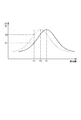
上記ギャップが増大すると、交流信号に対するインダクタンスL及びキャパシタンスCが共に低下し、逆に、ギャップが減少すると、インダクタンスL及びキャパシタンスCが共に上昇する。従って、ギャップの変化により、LC回路の自己共振周波数f(=1/(2π(L・C)1/2))が変化する。
図2は、LC回路の周波数特性の一例を示すグラフである。周波数特性は、例えば自己共振周波数f1でピークとなる実線の曲線であるが、自己共振周波数が低下してf2になると、周波数特性は破線の曲線となる。この結果、LC回路に一定の発振周波数f0を供給している場合において、LC回路の出力(振幅)は、V1からV2に変化する。このようにして、ギャップの変化を出力の変化として検出することができる。
When the gap increases, both the inductance L and the capacitance C with respect to the AC signal decrease, and conversely, when the gap decreases, both the inductance L and the capacitance C increase. Therefore, the self-resonant frequency f (= 1 / (2π (L · C) 1/2 )) of the LC circuit changes due to the change in the gap.
FIG. 2 is a graph showing an example of frequency characteristics of the LC circuit. The frequency characteristic is, for example, a solid curve that peaks at the self-resonant frequency f1, but when the self-resonant frequency decreases to f2, the frequency characteristic becomes a dashed curve. As a result, when the constant oscillation frequency f0 is supplied to the LC circuit, the output (amplitude) of the LC circuit changes from V1 to V2. In this way, a change in gap can be detected as a change in output.
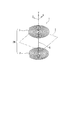
次に、本発明の一実施形態に係る基板形複層コイル1について説明する。図3は、当該基板形複層コイル1を示す斜視図である。ここで、図示のX,Y,Zは、互いに直交する3方向である。
図において、X−Z平面上で、導電部を渦巻状に形成して成る面状のコイル3は、渦巻の中心線方向(Y方向)へ複層(2層)に設けられ、全体として複層コイル3Mを構成している。隣接するコイル3間には、絶縁層としてのフレキシブルプリント基板2が介在している。フレキシブルプリント基板2には、図示しないスルーホールに沿って導電路5が形成されている。この導電路5を介して、上下のコイル3が互いに接続されている。なお、図を見易くするために2つのコイル3を互いに上下に引き離して表しているが、実際には、2つのコイル3は、薄いフレキシブルプリント基板2を挟んで背中合わせになっている。
Next, the board | substrate type multilayer coil 1 which concerns on one Embodiment of this invention is demonstrated. FIG. 3 is a perspective view showing the substrate type multilayer coil 1. Here, X, Y, and Z shown in the figure are three directions orthogonal to each other.
In the figure, a
2つのコイル3は、同じ方向(例えば上方)から見ると互いに逆の渦巻であるが、電流という視点から見ると、同じ方向に巻いている。すなわち、仮に、上のコイル3の外側の巻端から電流が流れ込んだ場合、電流は右巻きに渦の中心へ向かい、下のコイル3に達すると、今度は、右巻きに渦の外側へ向かい、下のコイル3の外側の巻端に達する。従って、電流は常に右巻きに流れており、右巻きのターン数が累積される。電流が逆に流れるときは、電流は常に左巻きに流れ、左巻きのターン数が累積される。
The two
このようにして、厚さ方向(渦巻の中心線方向)には極めて薄い基板形複層コイル1でありながら、1個のコイル3の2倍のターン数を確保することができる。従って、所望のインダクタンスを容易に得ることができる。また、複層化により、コイルが設けられる面領域の増大を抑制することができる。
さらに、スルーホールの導電路5によって層間の接続を行うので、導電路5の長さは実質的に最短距離であり、無駄がない。また、2つのコイル3の渦巻中心がずれないので、磁束の相殺が生じにくく、無駄なくインダクタンスを獲得することができる。
In this manner, the number of turns twice as large as that of one
Furthermore, since the layers are connected by the
一方、2つのコイル3は互いに逆の渦巻きであり、同一形態ではないため、X−Z平面で通し見た2つのコイル3は、重なっている部分と、重ならない部分とがあり、この重ならない部分があることで、全体として、1個のコイルよりもパターン面積が増大することになる。このため、Y方向に金属製の物体が存在するとして、複層コイル3Mに交流信号を与えたとき、当該物体との間に現れるキャパシタンスは、単層コイルの場合より大きくなる。すなわち、コイルの複層化により、対物キャパシタンスを増大させることができる。
On the other hand, since the two
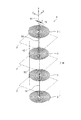
次に、本発明の他の実施形態に係る基板形複層コイル1について説明する。図4は、当該基板形複層コイル1を示す斜視図である。この構成は、図3よりもさらに基板形複層コイル1の複層化を発展させたものである。
図において、X−Z平面上で導電部を渦巻状に形成して成る面状のコイル3は、渦巻の中心線方向(Y方向)へ複層(4層)に設けられ、全体として複層コイル3Mを構成している。隣接するコイル3間には、絶縁層としてのフレキシブルプリント基板2が介在している。フレキシブルプリント基板2には、スルーホールh1,h2,h3に沿ってそれぞれ導電路51,52,53が形成されている。スルーホールh1,h2は、一方向(この例ではZ方向)にピッチPで並んでいる。図3と比較すると、ピッチPの分だけ、複層コイル3Mの全体としてのZ方向寸法は大きくなるが、X方向の寸法は同じである。
Next, a substrate type multilayer coil 1 according to another embodiment of the present invention will be described. FIG. 4 is a perspective view showing the substrate type multilayer coil 1. This configuration is a further development of the multi-layered substrate-type multi-layer coil 1 than in FIG.
In the figure, a
コイル3について上から順に第1〜4層とすると、第1層のコイル3の内側の巻端と第2層のコイル3の内側の巻端とは、導電路51を介して互いに接続されている。第2層のコイル3の外側の巻端と第3層のコイル3の外側の巻端とは、導電路53を介して互いに接続されている。そして、第3層のコイル3の内側の巻端と第4層のコイル3の内側の巻端とは、導電路52を介して互いに接続されている。こうして、合計4層のコイル3が互いに直列接続されている。
Assuming that the
また、合計4層のコイル3のうち、隣接するコイル同士では渦巻の巻き方向が逆になっている。すなわち、第1層のコイル3と第2層のコイル3とでは渦巻の巻き方が互いに逆であり、第2層のコイル3と第3層のコイル3とでは渦巻の巻き方が互いに逆であり、さらに、第3層のコイル3と第4層のコイル3とでは渦巻の巻き方が互いに逆である。
なお、図を見易くするために4つのコイル3を互いに上下に引き離して表しているが、実際には、隣接する2つのコイル間に、フレキシブルプリント基板2を挟んで、全体として厚さの薄い基板形複層コイル1が構成されている。
Moreover, among the
In order to make the figure easy to see, the four
4つのコイル3は、同じ方向(例えば上方)から見ると交互に逆の渦巻であるが、電流という視点から見ると、同じ方向に巻いている。すなわち、仮に、第1層のコイル3の外側の巻端から電流が流れ込んだ場合、電流は右巻きに渦の中心へ向かい、導電路51を通って第2層のコイル3に達すると、今度は、右巻きに渦の外側へ向かい、第2層のコイル3の外側の巻端に達する。続いて、導電路53を通って第3層のコイル3の外側の巻端に達した電流は、右巻きに渦の中心へ向かい、導電路52を通って第4層のコイル3に達すると、今度は、右巻きに渦の外側へ向かい、第4層のコイル3の外側の巻端に達する。
従って、電流は常に右巻きに流れており、右巻きのターン数が累積される。電流が逆に流れるときは、電流は常に左巻きに流れ、左巻きのターン数が累積される。
The four
Therefore, the current always flows in the clockwise direction, and the number of clockwise turns is accumulated. When the current flows in reverse, the current always flows counterclockwise and the number of counterclockwise turns is accumulated.
このようにして、厚さ方向(渦巻の中心線方向)には極めて薄い基板形複層コイル1でありながら、1個のコイル3の4倍のターン数を確保することができる。従って、所望のインダクタンスを容易に得ることができる。また、複層化により、コイルが設けられる面領域の増大を抑制することができる。
さらに、スルーホールの導電路5によって層間の接続を行うので、導電路5の長さは実質的に最短距離であり、無駄がない。また、4つのコイル3の渦巻中心がほとんどずれないので、磁束の相殺が生じにくく、無駄なく大きなインダクタンスを獲得することができる。
In this way, the number of turns four times that of one
Furthermore, since the layers are connected by the
一方、4つのコイル3は交互に逆の渦巻きであり、かつ、1つおきに同じ巻き方の渦巻であっても2つの巻端の位置が同じではない。すなわち、4つのコイル3は、相互に同一形態ではない。従って、X−Z平面で通し見た4つのコイル3は、重なっている部分と、重ならない部分とがあり、この重ならない部分があることで、全体として、1個のコイルよりもパターン面積が増大することになる。このため、図3の構成の場合と同様に、コイルの複層化により、対物キャパシタンスを増大させることができる。
On the other hand, the four
なお、図4でコイル3を4層としたのは一例に過ぎず、必要に応じてさらに多層としてもよいし、奇数層の構成であってもよい。基本的には2層以上であればよい。複層コイル全体としての両方の巻端を共に渦巻の外側とするためには、図4の構成を基本とした偶数層にすればよい。
この場合、複層の数が増えるとZ方向に並ぶスルーホールの数が増えて複層コイル3Mが占有する面積がその方向に徐々に拡がるが、X方向には拡がらない。従って、X方向に関しては、複層の数に関係なく一定のコンパクトな寸法とすることができる。
In FIG. 4, the
In this case, as the number of multilayers increases, the number of through holes arranged in the Z direction increases and the area occupied by the
なお、スルーホールには貫通タイプと、非貫通タイプとがあり、図4は、スルーホールh1,h2,h3が非貫通であるように描いている。しかしながら、実際には貫通スルーホールが一般的である。図5は、貫通スルーホールの存在を前提とした、図4と同様の基板形複層コイルを示す斜視図である。この場合、各スルーホールは4層全てにわたって存在している。 Note that there are a through-hole type and a non-through-type in the through hole, and FIG. 4 is drawn so that the through holes h1, h2, and h3 are not through. However, in practice, through-holes are common. FIG. 5 is a perspective view showing a substrate-type multilayer coil similar to that in FIG. In this case, each through hole exists over all four layers.
なお、図4,図5では渦巻の巻き方が順に逆になるような構成に基づいてスルーホールを利用したが、原理的には電流の巻き方向が同一になるように全てのコイルを直列接続することができればよい。
例えば図11は、同じ巻き方の渦巻であるコイル3を4層に構成した基板形複層コイル1を示す斜視図である。この場合の導電路5は、一のコイル3の内側の巻端と、隣接する他のコイル3の外側の巻端とを繋ぐ必要があるので、図4,図5のように簡単な構成ではない。しかし、例えば、導電路5を含む層(この例では全部で3層)を余分に用意すれば、全体の層数は増えるが(4+3層)、実現可能な構成ではある。
4 and 5, the through holes are used based on the configuration in which the spiral winding method is reversed in order, but in principle, all the coils are connected in series so that the current winding directions are the same. I can do it.
For example, FIG. 11 is a perspective view showing a substrate-type multilayer coil 1 in which coils 3 that are spirals of the same winding method are configured in four layers. In this case, the
なお、上述のような基板形複層コイル1は、フレキシブルプリント基板2の使用により、容易に、曲面状(典型的には円筒状)とすることができる。従って、例えば円柱状又は円筒状の物体の表面に沿わせるセンサを構成するには好適である。
The substrate-type multilayer coil 1 as described above can be easily curved (typically cylindrical) by using the flexible printed
次に、上記のような基板形複層コイル1を用いた本願発明の一実施形態に係る変位センサ装置について説明する。
図6の(a)は、変位センサ装置に用いられる基板形センサ10の展開図である。この基板形センサ10においては、フレキシブルプリント基板2上に、4個の複層コイル3M(各個共通の符号)が2段に、合計8個設けられている。なお、図では複層コイル3Mを簡略化して同心円のように描いているが、実際は、図3や図4に示したような渦巻である(以下、同様。)。
Next, a displacement sensor device according to an embodiment of the present invention using the substrate type multilayer coil 1 as described above will be described.
FIG. 6A is a development view of the
ここで、各コイル個別の符号は、後述の回転体の軸方向をY方向とした場合に、Y方向に直交し、かつ、互いに直交するX方向・Z方向に対応し、数字はY軸上の組番号、+、−はX,Z方向の組を表している。すなわち、変位を検出するためのコイルの組み合わせは、以下のようになる。
X方向変位:(X1+,X1−)、(X2+,X2−)
Z方向変位:(Z1+,Z1−)、(Z2+,Z2−)
各複層コイル3Mにおける2つの巻端(図示せず。)は、フレキシブルプリント基板2の表裏両面の導電路6を経て、端子電極部2aに導出されている。
Here, the individual codes for the coils correspond to the X direction and Z direction orthogonal to the Y direction and orthogonal to each other when the axial direction of the rotating body described later is the Y direction. The combination number, +,-represents a set in the X and Z directions. That is, the combination of coils for detecting displacement is as follows.
X-direction displacement: (X1 +, X1-), (X2 +, X2-)
Z-direction displacement: (Z1 +, Z1-), (Z2 +, Z2-)
Two winding ends (not shown) in each
このような基板形センサ10を円筒状に丸めると、(b)に示すようになり、コイルX1+及びX1−、並びに、X2+及びX2−は、それぞれ、X方向に2個1組の存在となる。また、コイルZ1+及びZ1−、並びに、Z2+及びZ2−は、それぞれ、Z方向に2個1組の存在となる。また、上段側及び下段側の各4個のコイルは、周方向の位相90度ごとに配置されている。
When such a substrate-
図7は、丸めた状態のフレキシブルプリント基板2を支持し、かつ、その円筒形状を維持すべく、円筒状の支持部11の内周面上に取り付ける状態を示す斜視図である。内周面にフレキシブルプリント基板2を固定するには、例えば、耐熱樹脂接着剤を使用することができる。支持部11は、樹脂製であってもよいが、ここでは金属製とする。金属製の場合、機械的強度を容易に確保することができるので、樹脂製に比べて薄肉の支持部とすることができる。このことは、コンパクト化に寄与する。なお、支持部が金属製であっても、高周波信号(100kHz〜500kHz)でLC回路を駆動することにより、変位検出に影響がないことが確認された。
FIG. 7 is a perspective view showing a state in which the flexible printed
支持部11の内周面に固定されたフレキシブルプリント基板2の内側には、径方向の微小な隙間を確保して、検出対象物としての回転体12が挿入される。この回転体12とは例えば自動車の車軸である。その場合、支持部11は転がり軸受装置の固定輪に取り付けられ、可動輪に回転体(車軸)12が取り付けられている。そして、上記の隙間は、転がり軸受装置によって維持される。
On the inner side of the flexible printed
図8の(a)は、支持部11の図示を省略して、フレキシブルプリント基板2の内側に回転体12が挿通されている状態を示している。(b)は、これを回転体12の軸方向から見た図である。フレキシブルプリント基板2と回転体12の表面との間には径方向へのギャップ(例えば3mm程度)があり、このギャップの変化によって、前述のインダクタンスL,キャパシタンスCが変化する。従って、車輪に荷重が作用した際に発生する車軸の径方向の変位を、前述の出力の変化として検出することができる。
FIG. 8A shows a state where the
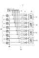
図9は、変位センサ装置20の回路構成の一例を示す回路図である。変位センサ装置20は、基板形センサ10に搭載された複層コイル3Mの他、信号処理回路17を備えている。各コイルは前述のように等価的にはLC回路であり、発振回路13から抵抗14を介して所定の発振周波数f0の交流信号が供給される。LC回路の出力はインピーダンス変換を行うバッファ回路(電圧フォロワ回路)15を経て、差動増幅回路16に入力される。
FIG. 9 is a circuit diagram illustrating an example of a circuit configuration of the
差動増幅回路16は、対を成す2つのLC回路からの信号電圧の差をとることで信号の線形化を行い、かつ、増幅を行う。線形化によって、回転体12の径方向への変位を正確に検出することができる。すなわち、軸方向に直交する方向にコイルを2個1組で設け、出力の差をとることで、回転体12の径方向への変位を正確に検出することができる。差動増幅後の信号は、X方向の2出力(X1,X2)と、Z方向の2出力(Z1,Z2)として出力される。これらの4出力に基づいて、ECU(図示せず。)は車輪に作用する荷重を求める。また、同じ方向の2出力に基づいて、モーメント荷重を求めることができる。
なお、信号処理回路17は、基板形センサ10とは別に設けられるが、フレキシブルプリント基板2の空きスペースに実装することも可能である。
The
The
以上のように、上記実施形態に係る変位センサ装置20によれば、基板形複層コイル3Mを変位検出のセンサとすることで、所望のセンサ感度を得るためにセンサのコイルに必要となるインダクタンスを確保しつつ、軽量・コンパクトな変位センサ装置を提供することができる。
また、フレキシブルプリント基板2は変形容易であり、回転体12の表面に自在に近接させることができる。近接によって、複層コイル3Mの導電部と回転体12との間にキャパシタンスが現れるので、別途、回路部品としてのコンデンサを用意することなく、LC回路を構成することができる。
また、1つの基板に必要数の複層コイル3Mを設けることができ、それによって、僅か1枚のフレキシブルプリント基板2に必要な機能を集約することができる。
As described above, according to the
Moreover, the flexible printed
In addition, a necessary number of
上記各実施形態に係る変位センサ装置20は、例えば、自動車の車輪を回転自在に支持する転がり軸受装置に搭載することができる。
図10は、転がり軸受装置の一種であるハブユニットの断面図である。このハブユニット100は車両に取り付けられるものであり、取り付けた状態では、図10における右側が車両のアウター側(車両の外側)であり、左側が車両のインナー側(車両の内側)である。図10において、ハブユニット100の中心軸Cに沿った方向をY方向とし、これに直交する紙面に垂直な方向をX方向とし、Y方向及びX方向の双方に直交する鉛直方向をZ方向とする。従って、このハブユニット100が自動車に取り付けられた状態においてX方向は車輪の前後水平方向となり、Y方向は車輪の左右水平方向(軸方向)となり、Z方向は上下方向となる。
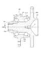
The
FIG. 10 is a cross-sectional view of a hub unit which is a kind of rolling bearing device. The
このハブユニット100は、主たる構造部分として、外輪101、内軸102、内輪部材103、ナット104、及び、転動体105を備えている。外輪101は、筒状部101aと、この筒状部101aの一部の外周面から径方向外方へ伸びたフランジ部101bとを有している。このフランジ部101bは、車体側の固定部材(図示せず。)に固定され、これによってハブユニット100が車体に固定される。内軸102は、外輪101内に挿通される主軸部102aと、車両アウター側にあって径方向外方へ延びるフランジ部102bとを有している。このフランジ部102bが、車輪のホイールやブレーキディスクの取付部となる。なお、主軸部102aは、前述の回転体12(図7)に相当する部分である。
The
内軸102の車両インナー側には、筒状の内輪部材103が外嵌され、さらに、内軸102の端部に形成された雄ねじ部102dにナット104が螺着されることにより、内輪部材103が内軸102に固定されている。転動体105は、周方向に複数個配置された玉からなる複列の構成となっている。各列の玉は保持器(図示せず。)によって周方向に所定間隔で保持されている。
このハブユニット100において、外輪101は、車体側の固定部材に固定される固定軌道輪である。また、内軸102と内輪部材103とは、外輪101に転動体105を介して回転自在に支持された回転軌道輪である。外輪101、内軸102及び内輪部材103は、互いに同軸(中心軸C)に配置されている。
A cylindrical
In the
このように構成されたハブユニット100において、図7の基板形センサ10を、支持部11と共に、外輪101の内周面上に取り付けることにより、内軸102の変位を検出することができる。
この場合、基板形センサ10等を搭載しつつも、コンパクトなハブユニット100を提供することができる。すなわち、従来は搭載不可能であった転がり軸受装置の内外輪間のような狭い場所にも、基板形センサを搭載することができるようになる。
In the
In this case, it is possible to provide a
なお、上記各実施形態の基板形複層コイル1は、変位センサ以外にも、各種用途のインダクタとして使用可能である。
また、上記実施形態の変位センサ装置20は、転がり軸受装置に限らず種々の装置の変位検出に用いることができる。また、ターゲットを周期的に検出すれば、変位検出に基づいて速度検出や回転数検出も行うことができる。
また、変位センサ装置における検出対象物は回転体に限られるものではなく、軸動型の機器や、往復動の機器等、種々の機器において変位を生じる物体を検出対象とすることができる。
In addition, the board | substrate type multilayer coil 1 of said each embodiment can be used as an inductor of various uses besides a displacement sensor.
Further, the
In addition, the detection target in the displacement sensor device is not limited to a rotating body, and an object that causes displacement in various devices such as an axial-type device and a reciprocating device can be detected.
1 基板形複層コイル
2 フレキシブルプリント基板(絶縁層)
3 コイル
3M 複層コイル
5 導電路
12 回転体(検出対象物)
17 信号処理回路
20 変位センサ装置
51〜53 導電路
h1,h2,h3 スルーホール
1
17
Claims (2)
フレキシブルプリント基板により構成され、隣接する前記コイル間に介在する絶縁層と、 前記絶縁層に設けられ、全ての前記コイルを、電流の巻き方向が同一になるよう直列接続する導電路とを備え、
前記複層コイルは、隣接するコイル同士では渦巻の巻き方向が互いに逆であり、
前記導電路は、前記絶縁層に設けられたスルーホールに沿って形成され、前記コイルの内・外いずれか一方の巻端を、隣接する他のコイルの当該一方の巻端と接続することにより全ての前記コイルを直列接続し、
前記スルーホールは全ての前記絶縁層を貫くものであり、当該スルーホールは前記中心線方向と直交する一方向に並んでいることを特徴とする基板形複層コイル。 A multilayer coil in which a planar coil formed by forming a conductive portion in a spiral shape is provided in multiple layers in the direction of the center line of the spiral;
An insulating layer that is configured by a flexible printed circuit board and is interposed between the adjacent coils; and a conductive path that is provided in the insulating layer and that connects all the coils in series so that the current winding direction is the same .
In the multilayer coil, adjacent coils have mutually opposite spiral winding directions,
The conductive path is formed along a through-hole provided in the insulating layer, and the winding end of either the inner or outer side of the coil is connected to the one winding end of another adjacent coil. All the coils are connected in series,
The substrate-type multilayer coil , wherein the through holes penetrate all the insulating layers, and the through holes are arranged in one direction orthogonal to the center line direction .
導電部を渦巻状に形成して成る面状のコイルを渦巻の中心線方向へ複層に設けたものであり、渦巻面が前記検出対象物と対向する複層コイルと、
隣接する前記コイル間に介在する絶縁層と、
前記絶縁層に設けられ、全ての前記コイルを、電流の巻き方向が同一になるよう直列接続する導電路と、
前記複層コイルのインダクタンス及び前記複層コイルと前記検出対象物との間に現れるキャパシタンスによって構成されるLC回路を交流信号で駆動したときの出力信号を抽出する信号処理回路とを備え、
前記複層コイルは、隣接するコイル同士では渦巻の巻き方向が互いに逆であり、
前記導電路は、前記絶縁層に設けられたスルーホールに沿って形成され、前記コイルの内・外いずれか一方の巻端を、隣接する他のコイルの当該一方の巻端と接続することにより全ての前記コイルを直列接続し、
前記スルーホールは全ての前記絶縁層を貫くものであり、当該スルーホールは前記中心線方向と直交する一方向に並んでいることを特徴とする変位センサ装置。 A displacement sensor device for detecting a displacement of a metal detection object in a non-contact manner,
A coil formed by forming a conductive portion in a spiral shape in a multilayer in the direction of the center line of the spiral, and a multilayer coil in which the spiral surface faces the detection object;
An insulating layer interposed between adjacent coils;
A conductive path provided in the insulating layer and connecting all the coils in series so that the current winding direction is the same;
A signal processing circuit that extracts an output signal when an LC circuit constituted by an inductance of the multilayer coil and a capacitance appearing between the multilayer coil and the detection object is driven by an AC signal ;
In the multilayer coil, adjacent coils have mutually opposite spiral winding directions,
The conductive path is formed along a through-hole provided in the insulating layer, and the winding end of either the inner or outer side of the coil is connected to the one winding end of another adjacent coil. All the coils are connected in series,
The through-hole penetrates all the insulating layers, and the through-hole is arranged in one direction orthogonal to the center line direction .
Priority Applications (1)
| Application Number | Priority Date | Filing Date | Title |
|---|---|---|---|
| JP2008294722A JP5347446B2 (en) | 2008-11-18 | 2008-11-18 | Substrate type multilayer coil and displacement sensor device |
Applications Claiming Priority (1)
| Application Number | Priority Date | Filing Date | Title |
|---|---|---|---|
| JP2008294722A JP5347446B2 (en) | 2008-11-18 | 2008-11-18 | Substrate type multilayer coil and displacement sensor device |
Publications (3)
| Publication Number | Publication Date |
|---|---|
| JP2010122012A JP2010122012A (en) | 2010-06-03 |
| JP2010122012A5 JP2010122012A5 (en) | 2012-10-11 |
| JP5347446B2 true JP5347446B2 (en) | 2013-11-20 |
Family
ID=42323485
Family Applications (1)
| Application Number | Title | Priority Date | Filing Date |
|---|---|---|---|
| JP2008294722A Expired - Fee Related JP5347446B2 (en) | 2008-11-18 | 2008-11-18 | Substrate type multilayer coil and displacement sensor device |
Country Status (1)
| Country | Link |
|---|---|
| JP (1) | JP5347446B2 (en) |
Families Citing this family (16)
| Publication number | Priority date | Publication date | Assignee | Title |
|---|---|---|---|---|
| JP2012156281A (en) * | 2011-01-26 | 2012-08-16 | Yazaki Corp | Air-core coil |
| EP2792528B1 (en) | 2011-12-13 | 2018-09-05 | Amiteq Co., Ltd. | Position detection device |
| CN102982969B (en) * | 2012-11-27 | 2015-09-16 | 宁波澳普网络通信设备有限公司 | Pulse transformer |
| CN105308418B (en) | 2013-06-13 | 2018-05-08 | 株式会社阿米泰克 | induction type position detecting device |
| JP6201718B2 (en) * | 2013-12-17 | 2017-09-27 | 三菱電機株式会社 | Inductor, MMIC |
| JP6567329B2 (en) * | 2014-06-20 | 2019-08-28 | 日本特殊陶業株式会社 | Resonator |
| KR20170001295A (en) * | 2015-06-26 | 2017-01-04 | 엘지전자 주식회사 | Compressor and Chiller system including it |
| WO2017078110A1 (en) | 2015-11-04 | 2017-05-11 | 株式会社アミテック | Displacement detection device |
| CN108061509B (en) * | 2016-11-08 | 2023-07-11 | 新思考电机有限公司 | Position detecting device, lens driving device, camera device, and electronic apparatus |
| US11304642B2 (en) * | 2017-02-15 | 2022-04-19 | Biosense Webster (Israel) Ltd. | Multi-axial position sensors printed on a folded flexible circuit board |
| CN107464674B (en) * | 2017-09-29 | 2019-04-05 | 中国工程物理研究院电子工程研究所 | A kind of electric-force gradient gradual change transformer and flexible circuit potential device |
| JP7178668B2 (en) | 2018-01-23 | 2022-11-28 | 株式会社アミテック | Inductive rotation detector |
| CN218297031U (en) * | 2020-03-12 | 2023-01-13 | 雅马哈株式会社 | Displacement sensor and musical performance operating device |
| WO2024013824A1 (en) * | 2022-07-11 | 2024-01-18 | 日立Astemo株式会社 | Planar coil array and displacement sensor |
| WO2024013825A1 (en) * | 2022-07-11 | 2024-01-18 | 日立Astemo株式会社 | Planar coil array and displacement sensor |
| JP7283000B1 (en) | 2022-07-11 | 2023-05-29 | 日立Astemo株式会社 | Planar coil array and displacement sensor |
Family Cites Families (2)
| Publication number | Priority date | Publication date | Assignee | Title |
|---|---|---|---|---|
| JPS58124918U (en) * | 1982-02-17 | 1983-08-25 | オリンパス光学工業株式会社 | Laminated printed coil board |
| JP2007127253A (en) * | 2005-11-07 | 2007-05-24 | Jtekt Corp | Rolling bearing device with sensor |
-
2008
- 2008-11-18 JP JP2008294722A patent/JP5347446B2/en not_active Expired - Fee Related
Also Published As
| Publication number | Publication date |
|---|---|
| JP2010122012A (en) | 2010-06-03 |
Similar Documents
| Publication | Publication Date | Title |
|---|---|---|
| JP5347446B2 (en) | Substrate type multilayer coil and displacement sensor device | |
| JP5094390B2 (en) | Position sensor | |
| JP5434585B2 (en) | Displacement sensor device and rolling bearing device | |
| JP2010122012A5 (en) | ||
| CN106460940B (en) | Rotary transformer bearing, rotary transformer stator and its manufacturing method | |
| JPH04222447A (en) | Resolver having flat winding | |
| JP2010127744A (en) | Displacement sensor apparatus and roller bearing apparatus | |
| CN104567651A (en) | PCB planar differential inductive angular displacement sensor | |
| US9065309B2 (en) | Magnetic levitation type vacuum pump and magnetic levitation device | |
| JP5195336B2 (en) | Displacement sensor device and rolling bearing device | |
| JP4982756B2 (en) | motor | |
| JP5440205B2 (en) | Displacement sensor device and rolling bearing device | |
| JP2010133782A (en) | Rolling bearing assembly | |
| JP5434577B2 (en) | Displacement sensor device and rolling bearing device | |
| JP5133758B2 (en) | Position sensor device for magnetic bearing and magnetic bearing device | |
| JP5387013B2 (en) | Manufacturing method of substrate type sensor | |
| JP2006126130A (en) | Magnetostrictive torque sensor | |
| JP2008286219A (en) | Bearing device and bearing preload detecting device | |
| JP5218101B2 (en) | Displacement sensor device and rolling bearing device | |
| JP2011185656A (en) | Resolver | |
| JP6199628B2 (en) | Superconducting coil device | |
| JP2011136401A (en) | Spindle device | |
| JP5030744B2 (en) | Bearing device | |
| JP2017096825A (en) | Torque measurement sensor and bearing with sensor | |
| JP5176991B2 (en) | Substrate type sensor |
Legal Events
| Date | Code | Title | Description |
|---|---|---|---|
| A621 | Written request for application examination |
Free format text: JAPANESE INTERMEDIATE CODE: A621 Effective date: 20110927 |
|
| A521 | Request for written amendment filed |
Free format text: JAPANESE INTERMEDIATE CODE: A523 Effective date: 20120718 |
|
| A521 | Request for written amendment filed |
Free format text: JAPANESE INTERMEDIATE CODE: A523 Effective date: 20120829 |
|
| A977 | Report on retrieval |
Free format text: JAPANESE INTERMEDIATE CODE: A971007 Effective date: 20130116 |
|
| A131 | Notification of reasons for refusal |
Free format text: JAPANESE INTERMEDIATE CODE: A131 Effective date: 20130205 |
|
| A521 | Request for written amendment filed |
Free format text: JAPANESE INTERMEDIATE CODE: A523 Effective date: 20130315 |
|
| TRDD | Decision of grant or rejection written | ||
| A01 | Written decision to grant a patent or to grant a registration (utility model) |
Free format text: JAPANESE INTERMEDIATE CODE: A01 Effective date: 20130723 |
|
| A61 | First payment of annual fees (during grant procedure) |
Free format text: JAPANESE INTERMEDIATE CODE: A61 Effective date: 20130805 |
|
| R150 | Certificate of patent or registration of utility model |
Free format text: JAPANESE INTERMEDIATE CODE: R150 Ref document number: 5347446 Country of ref document: JP Free format text: JAPANESE INTERMEDIATE CODE: R150 |
|
| LAPS | Cancellation because of no payment of annual fees |