JP5331475B2 - Heat transfer surface for cooling electronic components - Google Patents
Heat transfer surface for cooling electronic components Download PDFInfo
- Publication number
- JP5331475B2 JP5331475B2 JP2008515836A JP2008515836A JP5331475B2 JP 5331475 B2 JP5331475 B2 JP 5331475B2 JP 2008515836 A JP2008515836 A JP 2008515836A JP 2008515836 A JP2008515836 A JP 2008515836A JP 5331475 B2 JP5331475 B2 JP 5331475B2
- Authority
- JP
- Japan
- Prior art keywords
- fins
- fin
- channels
- chip
- channel
- Prior art date
- Legal status (The legal status is an assumption and is not a legal conclusion. Google has not performed a legal analysis and makes no representation as to the accuracy of the status listed.)
- Expired - Fee Related
Links
Images


Classifications
-
- H—ELECTRICITY
- H05—ELECTRIC TECHNIQUES NOT OTHERWISE PROVIDED FOR
- H05K—PRINTED CIRCUITS; CASINGS OR CONSTRUCTIONAL DETAILS OF ELECTRIC APPARATUS; MANUFACTURE OF ASSEMBLAGES OF ELECTRICAL COMPONENTS
- H05K7/00—Constructional details common to different types of electric apparatus
- H05K7/20—Modifications to facilitate cooling, ventilating, or heating
-
- H—ELECTRICITY
- H01—ELECTRIC ELEMENTS
- H01L—SEMICONDUCTOR DEVICES NOT COVERED BY CLASS H10
- H01L23/00—Details of semiconductor or other solid state devices
- H01L23/34—Arrangements for cooling, heating, ventilating or temperature compensation ; Temperature sensing arrangements
- H01L23/42—Fillings or auxiliary members in containers or encapsulations selected or arranged to facilitate heating or cooling
- H01L23/427—Cooling by change of state, e.g. use of heat pipes
-
- B—PERFORMING OPERATIONS; TRANSPORTING
- B21—MECHANICAL METAL-WORKING WITHOUT ESSENTIALLY REMOVING MATERIAL; PUNCHING METAL
- B21J—FORGING; HAMMERING; PRESSING METAL; RIVETING; FORGE FURNACES
- B21J5/00—Methods for forging, hammering, or pressing; Special equipment or accessories therefor
- B21J5/06—Methods for forging, hammering, or pressing; Special equipment or accessories therefor for performing particular operations
- B21J5/068—Shaving, skiving or scarifying for forming lifted portions, e.g. slices or barbs, on the surface of the material
-
- F—MECHANICAL ENGINEERING; LIGHTING; HEATING; WEAPONS; BLASTING
- F28—HEAT EXCHANGE IN GENERAL
- F28F—DETAILS OF HEAT-EXCHANGE AND HEAT-TRANSFER APPARATUS, OF GENERAL APPLICATION
- F28F3/00—Plate-like or laminated elements; Assemblies of plate-like or laminated elements
- F28F3/02—Elements or assemblies thereof with means for increasing heat-transfer area, e.g. with fins, with recesses, with corrugations
- F28F3/04—Elements or assemblies thereof with means for increasing heat-transfer area, e.g. with fins, with recesses, with corrugations the means being integral with the element
- F28F3/048—Elements or assemblies thereof with means for increasing heat-transfer area, e.g. with fins, with recesses, with corrugations the means being integral with the element in the form of ribs integral with the element or local variations in thickness of the element, e.g. grooves, microchannels
-
- F—MECHANICAL ENGINEERING; LIGHTING; HEATING; WEAPONS; BLASTING
- F28—HEAT EXCHANGE IN GENERAL
- F28F—DETAILS OF HEAT-EXCHANGE AND HEAT-TRANSFER APPARATUS, OF GENERAL APPLICATION
- F28F3/00—Plate-like or laminated elements; Assemblies of plate-like or laminated elements
- F28F3/12—Elements constructed in the shape of a hollow panel, e.g. with channels
-
- H—ELECTRICITY
- H01—ELECTRIC ELEMENTS
- H01L—SEMICONDUCTOR DEVICES NOT COVERED BY CLASS H10
- H01L23/00—Details of semiconductor or other solid state devices
- H01L23/34—Arrangements for cooling, heating, ventilating or temperature compensation ; Temperature sensing arrangements
- H01L23/46—Arrangements for cooling, heating, ventilating or temperature compensation ; Temperature sensing arrangements involving the transfer of heat by flowing fluids
- H01L23/473—Arrangements for cooling, heating, ventilating or temperature compensation ; Temperature sensing arrangements involving the transfer of heat by flowing fluids by flowing liquids
-
- H—ELECTRICITY
- H01—ELECTRIC ELEMENTS
- H01L—SEMICONDUCTOR DEVICES NOT COVERED BY CLASS H10
- H01L2924/00—Indexing scheme for arrangements or methods for connecting or disconnecting semiconductor or solid-state bodies as covered by H01L24/00
- H01L2924/0001—Technical content checked by a classifier
- H01L2924/0002—Not covered by any one of groups H01L24/00, H01L24/00 and H01L2224/00
-
- Y—GENERAL TAGGING OF NEW TECHNOLOGICAL DEVELOPMENTS; GENERAL TAGGING OF CROSS-SECTIONAL TECHNOLOGIES SPANNING OVER SEVERAL SECTIONS OF THE IPC; TECHNICAL SUBJECTS COVERED BY FORMER USPC CROSS-REFERENCE ART COLLECTIONS [XRACs] AND DIGESTS
- Y10—TECHNICAL SUBJECTS COVERED BY FORMER USPC
- Y10T—TECHNICAL SUBJECTS COVERED BY FORMER US CLASSIFICATION
- Y10T29/00—Metal working
- Y10T29/49—Method of mechanical manufacture
- Y10T29/4935—Heat exchanger or boiler making
Description
関連出願の参照情報:本出願は、2005年6月7日に出願された、発明の名称が「電子部品冷却用の伝熱面」である米国特許仮出願第60/688,254号の優先権を主張し、上記米国仮出願の開示全てをここに援用して本文の記載の一部とする。 REFERENCE INFORMATION FOR RELATED APPLICATIONS: This application is a priority of US Provisional Application No. 60 / 688,254, filed Jun. 7, 2005, whose title is “Heat Transfer Surface for Cooling Electronic Components”. The entire disclosure of the above provisional application is hereby incorporated herein by reference.
本発明は、概して、伝導的に電子部品に取り付け可能であり且つその電子部品を冷却可能な冷却面に関する。 The present invention generally relates to a cooling surface that can be conductively attached to an electronic component and that can cool the electronic component.
コンピュータのような電子装置(デバイス)は、コンピュータチップの情報を処理するが、チップは使用中に熱を発生させる。チップがより早く又はより長時間情報を処理するほど、チップはより熱くなる。もしもチップが熱くなりすぎると、チップは焼き付いてしまうかさもなければ故障してしまう。従って、処理中のチップを冷却する構造が提供されている。例えば、コンピュータには、チップが熱くなりすぎつつあることをコンピュータが検知すると作動するファンが備えられている。さらに、コンピュータはまた、チップが熱くなりすぎつつあることをコンピュータが検知すると、処理速度を遅くする。これらの従来の冷却方法は、部品にダメージを与えるのを防ぐのに十分には電子部品を冷却しないため、しばしば効果的ではない。 An electronic device (device) such as a computer processes information on a computer chip, which generates heat during use. The faster the chip processes information for a longer time, the hotter the chip. If the chip gets too hot, the chip will burn or otherwise fail. Accordingly, a structure for cooling the chip being processed is provided. For example, a computer is equipped with a fan that operates when the computer detects that the chip is getting too hot. In addition, the computer also slows down processing speed when the computer detects that the chip is getting too hot. These conventional cooling methods are often not effective because they do not cool the electronic components sufficiently to prevent damage to the components.
他の従来の冷却装置及び方法において、伝導構造体がチップに隣接して取り付けられて、熱をチップから構造体へと逃がすように伝導する。このような構造体は様々な形状にすることが出来る。例えば、銅ブロックは、チップに取り付けられて、熱をチップからそれに取り付けられたブロックに伝導するようにされている。そのようなブロックの一つの表面には、伝熱を改良(強化)するために、フィンが取り付けられてきた。しかしながら、多くの場合、このような構造体では十分にチップを冷却できないので、結局チップは焼きついてしまうか、そうでなければ正常に機能しなくなる。 In other conventional cooling devices and methods, a conductive structure is attached adjacent to the chip to conduct heat away from the chip to the structure. Such a structure can have various shapes. For example, a copper block is attached to the chip and conducts heat from the chip to the block attached to it. Fins have been attached to one surface of such blocks to improve (enhance) heat transfer. However, in many cases, such a structure cannot cool the chip sufficiently, so that the chip will eventually burn or otherwise fail to function properly.
本発明は電子チップのような電子部品に、電子部品の冷却をより良く促進する冷却面を提供する。説明を容易にするために、冷却面は電子チップと共に用いられるものとして説明されているが、出願人は冷却面が電子チップと共にのみ用いられることを意図するものでは決してない。むしろ、当業者であれば、冷却面は、その冷却が促進されることが所望されているいかなる電子部品と共に用いられ得ることがわかるだろう。第1のチャネル(流路)組を画定する第1のフィン組が、冷却面の一方の側に備えられている。第1の組のフィンと第1の組のチャネルは、冷却面において第1の方向に向きが付けられている。第2のチャネル組を画定する第2のフィン組が、冷却面の、第1のフィン組及び第1のチャネル組と反対側に備えられている。第2の組のフィンと第2の組のチャネルは、冷却面において第2の方向に、好ましくは第1の方向に対して角度をなして、向きが付けられている。第1及び第2の組のチャネルを接続する通路が冷却面内を延在している。 The present invention provides a cooling surface for an electronic component such as an electronic chip that better facilitates cooling of the electronic component. For ease of explanation, the cooling surface has been described as being used with an electronic chip, but applicants are not intended to use the cooling surface only with an electronic chip. Rather, those skilled in the art will appreciate that the cooling surface can be used with any electronic component whose cooling is desired to be facilitated. A first fin set defining a first channel (flow channel) set is provided on one side of the cooling surface. The first set of fins and the first set of channels are oriented in a first direction at the cooling surface. A second fin set defining a second channel set is provided on the cooling surface opposite the first fin set and the first channel set. The second set of fins and the second set of channels are oriented in the second direction at the cooling surface, preferably at an angle to the first direction. A passage connecting the first and second sets of channels extends within the cooling surface.
冷却面は電子チップに取り付けられる。第1のフィン組のフィンの先端は、冷却面の(第1のフィンを介しての)電子チップへの取り付けを容易にするために、平坦にすることが出来る。液体冷媒が、少なくともチャネル組のうちの少なくとも一方に、好ましくは電子チップに直近の第1のチャネル組のチャネルに供給される。液体冷媒が冷却面に供給されるにつれ、第1のチャネル組のチャネルは液体冷媒で満たされる。液体冷媒は通路を流れて第2のチャネル組のチャネル内へと流れ込む。その際に、液体冷媒は第1及び第2のフィン組のフィンの壁面を被覆する。 The cooling surface is attached to the electronic chip. The tips of the fins of the first fin set can be flat to facilitate attachment of the cooling surface to the electronic chip (via the first fins). Liquid refrigerant is supplied to at least one of the channel sets, preferably to the channels of the first channel set proximate to the electronic chip. As liquid refrigerant is supplied to the cooling surface, the channels of the first channel set are filled with liquid refrigerant. The liquid refrigerant flows through the passage and into the channels of the second channel set. At that time, the liquid refrigerant covers the wall surfaces of the fins of the first and second fin sets.
電子チップの温度が上がると、冷却面はチップから熱を逃がす。熱は次いで、冷却面のフィンを被覆している冷媒に伝えられる。少なくとも液体冷媒のいくらかは蒸発し、その結果生じる蒸気が冷却面内の通路を通ってチップから離れて出て行く。 As the temperature of the electronic chip increases, the cooling surface releases heat from the chip. The heat is then transferred to the coolant covering the cooling surface fins. At least some of the liquid refrigerant evaporates and the resulting vapor exits the chip through a passage in the cooling surface.
電子部品冷却面、電子部品冷却面を形成する方法、電子部品冷却システムが提供される。 An electronic component cooling surface, a method of forming an electronic component cooling surface, and an electronic component cooling system are provided.
本発明は添付された特許請求の範囲の特徴を用いて説明されている。本発明の利点と特徴がより良く理解されるために、下記の図面及び説明を参照する。 The invention has been described using the features of the appended claims. For a better understanding of the advantages and features of the present invention, reference is made to the following drawings and description.
図1は、本発明の部分的に形成された面10の一実施形態を示している。面10は二組のフィン16、18(フィン16の組及びフィン18の組)によってそれぞれ形成された二組のチャネル12、14(チャネル12の組及びチャネル14の組)を含む。面10は、下側チャネル12の組がチップに隣接して位置付けられ且つ第1の方向に延在するように、並びに上側チャネル14の組が下側チャネル12の組の上方に位置付けられ且つ第1の方向と角度を成す第2の方向に延在するように、マイクロチップ(図に示されていない)に取り付けられることが好ましいが、そうである必要はない。チャネル12、14の組は、複数の通路20(図9参照)によって互いに連結されることが好ましい。
FIG. 1 illustrates one embodiment of a partially formed
面10は好ましくは伝導性材料、例えば金属(銅、チタン、アルミ、金、ステンレスなどを含む)の素材片(ブランク)から形成され、より好ましくは銅で形成される。しかしながら、面10は炭素含有量が多い炭化物のような、いかなる高伝導性素材から形成することが出来る。炭素それ自体を用いて面10を形成することが出来る。
The
図1は素材片11から形成された面10が部分的に形成された状態を示している。完成された面10においては、素材片11全体にわたってフィン16、18が形成されていることが好ましいが、そうである必要はない。面10を形成するために、直立する下側フィン16の組は素材片11の一方の側に形成され、それによって隣接するフィン16間に下側チャネル12の組が創出される。次いで、直立する上側フィン18の組は素材片11の下側フィン16の組と反対側に形成され、それによって隣接するフィン18間に上側チャネル14の組が創出される。フィン16、18の組は当技術分野において知られた多くの方法によって形成し得るが、フィン16、18の組をカットし次いでフィン16、18の組を所望の角度に持ち上げる(リフトする)ことによって作られることが好ましい。より具体的には、フィン16、18の組は、素材片11の表面をカットして層を作り、カットされた層を所望の角度にリフトし、それによって直立したフィン16、18の組が形成される。このカット及びリフト方法及び、この方法を行う工具は同時係属出願である米国特許出願公開第US2004/0069467号及び米国特許出願公開第US2005/0145377号において開示されており、それら開示の全てをここに援用して本文の記載の一部とする。フィン16、18の組を平坦な素材片に形成してもよいが、好ましい方法においては、カットされていない素材片が半円状に湾曲するように回転可能なドラムの周りに巻き付けられる。この形状において、素材片は管の表面を模倣し、管表面を改良(強化)する従来の技術を素材片のそれぞれの側に用いてフィン16、18を形成してもよい。フィン16、18の組のうちどちらを(そしてそれゆえに、チャネル12、14のチャネルのうちどちらを)先に素材片に形成しても違いはない。
FIG. 1 shows a state in which the
フィン16、18によって形成されたチャネル12、14が素材片11の厚みの中央線を越えて延在することが好ましいが、そうである必要はない。このように、通路20(図9参照)が下側チャネル12の組と上側チャネル14の組の交点において形成されて、下側チャネル12の組及び上側チャネル14の組の間を超えて延在する。チャネル12の、素材片の中央線を越えて延在する部分は、それに対応するチャネル14の部分であって、素材片の中央線を越えて延在する部分と交差する。この交差によって、通路20が2つのチャネル12、14の間に形成される。図9、10に通路20を示す。チャネル12の組及びチャネル14の組の両方が素材片の厚さの中央線を越えて延在することが好ましいが、チャネル12の組及びチャネル14の組のうち一方のみのチャネルが延在して通路20を形成してもよい。
Although it is preferred that the
図1のフィン16、18の組(そしてその結果形成されるチャネル12、14の組)は互いに垂直に方向付けられているものとして示されているが、フィン16の組とフィン18の組は互いに対していかなる角度を成して形成され得る。さらに、下側フィン16の組及び/又は上側フィン18の組内のフィン(そしてそれゆえに下側チャネル12の組及び/又は上側チャネル14の組内のチャネル)は、互いに平行である必要はない。
Although the set of
冷却面10上に作られ得るフィン16、18の数(そしてそれゆえにチャネル12、14の数)はいずれの数であってよい。本文で「フィンピッチ」という用語が用いられるが、これは単一のチャネルの幅にそのチャネルを画定するフィンのうちの一つの厚みを加えたものとして定義される。上側フィン18の組と下側フィン16の組のフィンピッチは、1インチ当たり20〜1,200個のフィン(1cm当たり約7.9〜約472.4個のフィン)であることが好ましいが、そうである必要はない。フィンピッチは、下側フィン16の組のフィンピッチが上側フィン18のフィンピッチと異なるように、下側フィン16の組と上側フィン18の組の間で変えてもよい。また、上側フィン18の一部のフィンが上側フィン18の別の一部のフィンと異なるフィンピッチを有するように、フィンピッチを上側フィン16の組と下側フィン18の組の各々において変えることも出来る。
The number of
さらにフィン16、18の高さ(そしてそれゆえに下側及び上側のチャネル12、14の深さ)もまた、下側フィン16の組のフィン高さが上側フィン18の組のフィン高さと異なるように、下側フィン16の組と上側フィン18の組との間で変えてもよい。同様に、上側フィン18の一部のフィンが上側フィン18の別の一部のフィンと異なるフィン高さを有するように、フィン高さを下側フィン16の組と上側フィン18の組の各々において変えることも出来る。
In addition, the height of the
フィン16の組及びフィン18の組、並びにチャネル12の組及びチャネル14の組の最適な幾何形状(ジオメトリー)は、用いられる冷媒の型と面10から取り除く必要のある熱の量とを含む、多くの要因に依って決まるであろう。フィン16の組及びフィン18の組各々のアスペクト比A(フィン高さ÷チャネル幅として規定される)は、好ましくは0.1<A<400の範囲であり、さらに好ましくは0.1<A<40の範囲であるが、そうである必要はない。
The optimum geometry of the set of
図3は面10の、1インチ当たり100個のフィン(1cm当たり約39.4個のフィン)のフィンピッチ及び0.023インチ(約0.0091cm)のフィン高さを有するフィン16によって形成された下側チャネル12の組の断面図である。図4は面10の、1インチ当たり200個のフィン(1cm当たり約78.7個のフィン)のフィンピッチ及び約0.0205インチ(約0.0081cm)のフィン高さを有するフィン18によって形成された上側チャネル14の組の断面図である。図5は面10の、1インチ当たり200個のフィン(1cm当たり約78.7個のフィン)のフィンピッチ及び約0.0175インチ(約0.0069cm)のフィン高さを有するフィン18によって形成された上側チャネル14の組の断面図である。図6は面10の、1インチ当たり200個のフィン(1cm当たり約78.7個のフィン)のフィンピッチ及び約0.021インチ(約0.0083cm)のフィン高さを有するフィン16によって形成された下側チャネル12の組の断面図である。図7はチャネル14を形成する上側フィン18の組の平面図である。
FIG. 3 is formed by
使用に際し、面10は、下側チャネル12の組がチップに直近となるようにチップに取り付けられることが好ましい。面10は、半田付け方法、接着剤又は糊を使用する方法など、いかなる数多くの方法でチップに取り付けることが出来る。チップの冷却を更に促進するために、接着剤又は糊は伝導性のものであることが好ましい。
In use,
チップへの面10の取り付け及び保持を促進するために、図2、3及び6で示されているように、下側フィン16の組のフィン先端が平坦にされることが好ましいが、そうである必要はない。このように先端を平坦にすることによって、チップに取り付ける為の付加的な表面積が創出される。さらに、下側フィン16の組の平坦にされたフィン先端によって創出された付加的な表面積は、熱伝導を支援する。図8はチャネル12を形成する下側フィン16の組の平面図である。下側フィン16の組のフィン先端は平坦にされている。
In order to facilitate attachment and retention of the
フィン16の組のフィン先端は従来技術又は米国特許出願公開第US2005/0145377号に記載されている技術を用いて平坦にし得る。米国特許出願公開第US2005/0145377号の開示全てをここに援用して本文の記載の一部とする。平坦化に加えて、フィン16の組のフィン先端はまた、曲げられて比較的平坦な表面を形成してもよいし、又は厚みをつけられた先端を有するようにカットされてもよく、これによって先端において取り付けのための付加的な表面積がさらに創出される。フィン先端を曲げるための及びフィン先端に厚みを付けるための方法及び工具もまた、隣接するフィンの先端に互いに角度をつける(これは本出願においても意図されている)ための方法及び工具と共に、米国特許出願公開第US2005/0145377号に記載されている。上側フィン18の組の、フィン先端を平坦にするか又はそうでなければ別な方法で強化することを、下側フィン16の組のフィン先端を平坦化することに加えて又はその代わりに行うことも、本発明の範囲内である。
The fin tips of the set of
チップの使用中に、チャネル12の組とチャネル14の組の少なくとも一方に液体冷媒が供給される。冷媒は少なくとも下側チャネル12の組に供給されることが好ましい。水と、3M社によって製造されたHFE―7100とを含むがそれらには限定されない数多くの冷媒が使用できる。代替的に、DuPont又はAllied Signalのような製造業者が134A又は123として知られている冷媒を製造しており、冷媒134A、123もまた本発明に使用されるのに好適である。冷媒は下側チャネル12の組に流れ込んで、下側フィン16の組のフィン表面を被覆する(覆う)。下側チャネル12の組が冷媒で満たされるにつれ、冷媒は通路20を通って放出され、そして上側チャネル14の組へと流れ込んで、少なくとも上側フィン18の組のいくつかのフィン表面を覆う。別の実施例において、冷媒は、下側チャネル12の組に供給する代わりに又はそれに加えて、上側チャネル14の組に直接供給してもよい。
During use of the chip, liquid refrigerant is supplied to at least one of the set of
チップによって発生した熱は伝導性面10に伝えられる。この伝熱の抗力によって、チャネル12、14内の液体冷媒の温度が上がり、少なくとも液体冷媒のいくらかを蒸気へと変える。下側チャネル12の組において発生された蒸気の少なくともいくらかは、通路20を通って上側チャネル12の組へと放出され、それによって熱がチップから運び去られる。さらに、蒸気化していない液体冷媒はチャネル12、14を通って流れてチャネル12、14から出て行くので、チップによって発生した熱はそのような冷媒中で運び去られる。このようにして、チップによって発生した熱は、液体又は蒸気の状態で冷媒によって運び去られる。
The heat generated by the chip is transferred to the
ポンプ(図示されていない)を使用して、液体冷媒をチャネル12、14の片方又は両方へと送り出して、それによって冷媒の全てが蒸気となることを防ぐことが出来る。あるいは、冷媒のいくらかが伝熱プロセス中に蒸気となってしまっても、ポンプは、液体冷媒と蒸気が組み合わされてチャネル12、14に存在するように、液体冷媒を冷却面10に補充する。ポンプは冷媒をチャネル12、14の組に供給し続けることが出来る。代替的に、ポンプのためのコントローラーを使用して、チップの温度を監視してもよいし、そして温度が前もって決められた温度まで上昇した時のみにポンプが作動するようにしてもよい。
A pump (not shown) can be used to pump liquid refrigerant to one or both of the
チャネル12、14の組に冷媒を(連続的に又はセンサ用いて)供給することにより、フィン16、18の組が確実に冷媒で覆われたままとなる。冷媒の薄膜のみがフィン16、18の組を覆うことが望ましい。伝熱係数は、チップから熱がどれだけ効率的に移し取られるかの指標である。伝熱係数が高いほど、熱は確実により効果的に移し取られる。冷媒の薄膜が好ましい理由は、伝熱係数がフィン16、18の冷媒層の厚さに反比例するためである。従って、冷媒の薄膜は高い伝熱係数を確保するので、それゆえに面10のチップから熱を移し取る性能を向上させる。
Supplying refrigerant (continuously or using a sensor) to the pair of
冷却面10に、フィン16の組とフィン18の組の二つのフィン組で形成されるチャネル12の組及びチャネル14の組の二つのチャネル組を備えることは、本出願において特に有益である。フィン16、18の2つのフィン組の形成によって、チャネルとフィンをそれぞれ1組しか持たない冷却面と比べて、面10のフィンの高さは実質的に2倍になり、その結果冷媒に接触するのに利用できる表面積も実質的に2倍になる。表面積が増加することで、より多くの熱をチップから取り去って冷媒へと伝熱することが可能となる。
It is particularly beneficial in this application to provide the
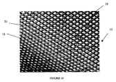
図1と9は、面10において、上側フィン18の組と上側チャネル14の組が下側フィン16の組と下側チャネル12の組に対して実質的に90度の角度がつけられて形成されていることを示している。しかしながら、上述したように、上側及び下側のフィン組並びにチャネル組は互いに対して90度の角度をなして向きが付けられる必要はない。むしろ、図10に示すように、上側及び下側のフィン組並びにチャネル組は互いに鋭角を成して形成されてよい。
FIGS. 1 and 9 show that in
本発明の一実施形態において、冷却面10は形成された後に伸張させる(ストレッチさせる)ことができる。伸張させることは、互いに鋭角を成して向きが付けられたフィン16、18の組及びチャネル12、14の組を有する面10に特に好適である。伸張させることによって製造上の便利さがもたらされる。具体的な用途のために意図された特性(フィンの高さ、ピッチ等)をそれぞれ有する様々な冷却面を製造するのに対して、単一の冷却面10を製造し、次いで冷却面10を特定の用途に合わせて調整するために伸張してもよい。たとえば、面10を伸張することによって、フィンピッチを増やすこと又はアスペクト比を変えることができる。さらに、上述したように、フィン16、18の組内における全てのフィンは同じフィンピッチを持つ必要はなく、又はフィン総数が同じである必要はなく、同じフィンピッチやフィン総数を有していないほうが却って望ましいこともあるであろう。冷却面10を伸張させることにより、フィン特性をフィン16、18の組内で選択的に変化させて冷却面10を特定の用途に合わせてよりよく調整することが可能になり、それによって冷却面10の効果を強化できる。図10は部分的に伸張された面10を示している。図10において、面10の左下隅の部分は、面10のそれ以外の部分よりも少ない度合いで伸張されている。
In one embodiment of the invention, the cooling
上記の説明は本発明の実施形態を示し、説明し且つ記載するためのものである。実施形態へのさらなる変更および改造は当業者にとって明らかであろうし、本発明の範囲又は精神を逸脱することなく変更および改造を行ってよい。 The foregoing description is intended to illustrate, describe and describe embodiments of the invention. Further changes and modifications to the embodiments will be apparent to those skilled in the art, and changes and modifications may be made without departing from the scope or spirit of the invention.
Claims (4)
a.第1の側と、第1の側と反対の第2の側とを有する素材片を提供することと、
b.素材片の第1の側から延在し且つ第1のチャネル組を画定する第1のフィン組を形成することと、
c.素材片の第2の側から延在し且つ第1のフィン組と鋭角をなして第2のチャネル組を画定する第2のフィン組を形成することと、
d.素材片内を延在し且つ第1及び第2のチャネル組を連結する複数の通路を形成することと、
e.フィンの少なくともいくつかを形成した後に素材片を伸張することと、
f.素材片を電子部品に取り付けること、とを含む方法。 A method of forming a cooling system for transferring heat from an electronic component, comprising:
a. Providing a piece of material having a first side and a second side opposite the first side;
b. Forming a first fin set extending from a first side of the blank and defining a first channel set;
c. Forming a second fin set extending from the second side of the blank and defining a second channel set at an acute angle with the first fin set;
d. Forming a plurality of passages extending through the blank and connecting the first and second channel sets;
e. Stretching the piece of material after forming at least some of the fins;
f. Attaching a piece of material to an electronic component.
第1のチャネル組又は第2のチャネル組の少なくともいくつかのチャネルが、素材片においてその厚さの半分を超えて延在して、素材片内を延在し且つ第1及び第2のチャネル組を連結する複数の通路を形成する請求項1に記載の方法。 The piece of material has a thickness,
At least some of the channels of the first channel set or the second channel set extend in the blank piece over half of its thickness and extend within the blank piece and the first and second channels The method of claim 1 , wherein a plurality of passages connecting the sets are formed.
Applications Claiming Priority (3)
| Application Number | Priority Date | Filing Date | Title |
|---|---|---|---|
| US68825405P | 2005-06-07 | 2005-06-07 | |
| US60/688,254 | 2005-06-07 | ||
| PCT/US2006/021959 WO2006133211A2 (en) | 2005-06-07 | 2006-06-06 | Heat transfer surface for electronic cooling |
Publications (3)
| Publication Number | Publication Date |
|---|---|
| JP2008543112A JP2008543112A (en) | 2008-11-27 |
| JP2008543112A5 JP2008543112A5 (en) | 2010-03-25 |
| JP5331475B2 true JP5331475B2 (en) | 2013-10-30 |
Family
ID=37499051
Family Applications (1)
| Application Number | Title | Priority Date | Filing Date |
|---|---|---|---|
| JP2008515836A Expired - Fee Related JP5331475B2 (en) | 2005-06-07 | 2006-06-06 | Heat transfer surface for cooling electronic components |
Country Status (9)
| Country | Link |
|---|---|
| US (2) | US7861408B2 (en) |
| EP (1) | EP1889528B1 (en) |
| JP (1) | JP5331475B2 (en) |
| KR (1) | KR20080012344A (en) |
| CN (1) | CN101287955B (en) |
| CA (1) | CA2605966A1 (en) |
| IL (2) | IL186705A0 (en) |
| MX (1) | MX2007015046A (en) |
| WO (1) | WO2006133211A2 (en) |
Families Citing this family (15)
| Publication number | Priority date | Publication date | Assignee | Title |
|---|---|---|---|---|
| KR20080012344A (en) * | 2005-06-07 | 2008-02-11 | 울버린 튜브, 인크. | Heat transfer surface for electronic cooling |
| CN102252557A (en) * | 2011-05-19 | 2011-11-23 | 山东北辰压力容器有限公司 | Rectangular longitudinal fin heat exchange element |
| US8963321B2 (en) | 2011-09-12 | 2015-02-24 | Infineon Technologies Ag | Semiconductor device including cladded base plate |
| US8519532B2 (en) | 2011-09-12 | 2013-08-27 | Infineon Technologies Ag | Semiconductor device including cladded base plate |
| US9238284B2 (en) * | 2011-12-20 | 2016-01-19 | Unison Industries, Llc | Methods for forming a heat exchanger and portions thereof |
| WO2015112771A2 (en) * | 2014-01-22 | 2015-07-30 | Wolverine Tube, Inc. | Double-sided micro fin plate for plate heat exchanger |
| US10201119B2 (en) * | 2015-06-02 | 2019-02-05 | Hamilton Sundstrand Corporation | System and method of alternate cooling of a liquid cooled motor controller |
| SG11201901751QA (en) * | 2016-09-01 | 2019-03-28 | Hs Mfg Group Llc | Methods for biobased derivatization of cellulosic surfaces |
| DE102017200422A1 (en) | 2017-01-12 | 2018-07-12 | Fraunhofer-Gesellschaft zur Förderung der angewandten Forschung e.V. | Process for the preparation of a heat exchanger and heat exchanger |
| EP3635319A1 (en) * | 2017-05-12 | 2020-04-15 | Carrier Corporation | Internally enhanced heat exchanger tube |
| US10520263B2 (en) | 2017-09-20 | 2019-12-31 | Toyota Motor Engineering & Manufacturing North America, Inc. | Apparatus, system, and method for interior fluid flow with optimized fin structures |
| KR102195183B1 (en) | 2019-09-06 | 2020-12-24 | 엘아이지넥스원 주식회사 | Integrated mast having a stealth function and its controlling method |
| JP7343166B2 (en) | 2019-11-13 | 2023-09-12 | ナカムラマジック株式会社 | Heat sink manufacturing method and heat sink |
| KR102264088B1 (en) | 2020-06-12 | 2021-06-11 | 엘아이지넥스원 주식회사 | Integrated mast having a IR stealth function and its controlling method |
| CN114121849A (en) * | 2020-08-27 | 2022-03-01 | 讯凯国际股份有限公司 | Water-cooling heat dissipation device and manufacturing method thereof |
Family Cites Families (30)
| Publication number | Priority date | Publication date | Assignee | Title |
|---|---|---|---|---|
| US3202212A (en) * | 1963-07-29 | 1965-08-24 | Peerless Of America | Heat transfer element |
| US4369838A (en) * | 1980-05-27 | 1983-01-25 | Aluminum Kabushiki Kaisha Showa | Device for releasing heat |
| JPS5870919A (en) * | 1981-10-23 | 1983-04-27 | Hitachi Cable Ltd | Manufacture of heat transmitting pipe |
| JPS5984095A (en) * | 1982-11-04 | 1984-05-15 | Hitachi Ltd | Heat exchanging wall |
| GB2149081B (en) * | 1983-11-01 | 1986-12-10 | Boc Group Plc | Heat exchangers |
| JPS60229353A (en) * | 1984-04-27 | 1985-11-14 | Hitachi Ltd | Heat transfering device |
| JPS60238698A (en) * | 1984-05-11 | 1985-11-27 | Hitachi Ltd | Heat exchange wall |
| JPH073844B2 (en) * | 1986-08-18 | 1995-01-18 | 株式会社日立製作所 | Heat transfer device |
| WO1990010537A1 (en) * | 1989-03-10 | 1990-09-20 | Hiroo Ichikawa | Reinforced composite corrugated body |
| JPH03209859A (en) * | 1990-01-12 | 1991-09-12 | Hitachi Ltd | Semiconductor cooling device |
| JP2550770B2 (en) * | 1990-10-11 | 1996-11-06 | 日本電気株式会社 | Electronic component cooling mechanism |
| DE4301668C1 (en) * | 1993-01-22 | 1994-08-25 | Wieland Werke Ag | Heat exchange wall, in particular for spray evaporation |
| RU2044606C1 (en) * | 1993-04-30 | 1995-09-27 | Николай Николаевич Зубков | Method of obtaining surfaces with alternative projections and hollows (variants) and tool for its realization |
| US5412535A (en) * | 1993-08-24 | 1995-05-02 | Convex Computer Corporation | Apparatus and method for cooling electronic devices |
| US5697430A (en) * | 1995-04-04 | 1997-12-16 | Wolverine Tube, Inc. | Heat transfer tubes and methods of fabrication thereof |
| US5761037A (en) * | 1996-02-12 | 1998-06-02 | International Business Machines Corporation | Orientation independent evaporator |
| US5642776A (en) * | 1996-02-27 | 1997-07-01 | Thermacore, Inc. | Electrically insulated envelope heat pipe |
| JPH1047884A (en) * | 1996-08-01 | 1998-02-20 | Mitsubishi Electric Corp | Heat exchanger |
| US5740014A (en) * | 1996-12-11 | 1998-04-14 | Lin; Chun Sheng | CPU heat sink |
| JPH10313080A (en) * | 1997-05-14 | 1998-11-24 | Toshiba Corp | Radiator and manufacture of the same |
| JP2000260916A (en) * | 1999-03-11 | 2000-09-22 | Hitachi Ltd | Heat sink |
| DE10024682C2 (en) * | 2000-05-18 | 2003-02-20 | Wieland Werke Ag | Heat exchanger tube for evaporation with different pore sizes |
| US7556086B2 (en) * | 2001-04-06 | 2009-07-07 | University Of Maryland, College Park | Orientation-independent thermosyphon heat spreader |
| US6766817B2 (en) * | 2001-07-25 | 2004-07-27 | Tubarc Technologies, Llc | Fluid conduction utilizing a reversible unsaturated siphon with tubarc porosity action |
| US6691769B2 (en) * | 2001-08-07 | 2004-02-17 | International Business Machines Corporation | Heat sink for convection cooling in horizontal applications |
| AU2003273835B2 (en) * | 2002-06-10 | 2009-08-20 | Wieland-Werke Ag | Heat transfer tube and method of and tool for manufacturing the same |
| US7311137B2 (en) | 2002-06-10 | 2007-12-25 | Wolverine Tube, Inc. | Heat transfer tube including enhanced heat transfer surfaces |
| US7104312B2 (en) * | 2002-11-01 | 2006-09-12 | Cooligy, Inc. | Method and apparatus for achieving temperature uniformity and hot spot cooling in a heat producing device |
| CN2667662Y (en) * | 2003-10-20 | 2004-12-29 | 林项武 | Integrated circuit heat pipe radiator |
| KR20080012344A (en) * | 2005-06-07 | 2008-02-11 | 울버린 튜브, 인크. | Heat transfer surface for electronic cooling |
-
2006
- 2006-06-06 KR KR1020077028492A patent/KR20080012344A/en not_active Application Discontinuation
- 2006-06-06 JP JP2008515836A patent/JP5331475B2/en not_active Expired - Fee Related
- 2006-06-06 EP EP06772321A patent/EP1889528B1/en active Active
- 2006-06-06 US US11/447,327 patent/US7861408B2/en not_active Expired - Fee Related
- 2006-06-06 MX MX2007015046A patent/MX2007015046A/en active IP Right Grant
- 2006-06-06 WO PCT/US2006/021959 patent/WO2006133211A2/en active Application Filing
- 2006-06-06 CN CN200680019882XA patent/CN101287955B/en not_active Expired - Fee Related
- 2006-06-06 CA CA002605966A patent/CA2605966A1/en not_active Abandoned
-
2007
- 2007-10-17 IL IL186705A patent/IL186705A0/en unknown
-
2010
- 2010-12-21 US US12/974,226 patent/US20110139411A1/en not_active Abandoned
-
2012
- 2012-01-25 IL IL217721A patent/IL217721A0/en unknown
Also Published As
| Publication number | Publication date |
|---|---|
| WO2006133211A3 (en) | 2008-01-17 |
| IL186705A0 (en) | 2008-02-09 |
| WO2006133211A2 (en) | 2006-12-14 |
| KR20080012344A (en) | 2008-02-11 |
| US20060283573A1 (en) | 2006-12-21 |
| IL217721A0 (en) | 2012-03-29 |
| EP1889528A4 (en) | 2011-09-07 |
| CA2605966A1 (en) | 2006-12-14 |
| EP1889528A2 (en) | 2008-02-20 |
| EP1889528B1 (en) | 2012-09-26 |
| MX2007015046A (en) | 2008-01-18 |
| CN101287955A (en) | 2008-10-15 |
| US7861408B2 (en) | 2011-01-04 |
| US20110139411A1 (en) | 2011-06-16 |
| CN101287955B (en) | 2010-09-29 |
| JP2008543112A (en) | 2008-11-27 |
Similar Documents
| Publication | Publication Date | Title |
|---|---|---|
| JP5331475B2 (en) | Heat transfer surface for cooling electronic components | |
| JP2008543112A5 (en) | ||
| US8756810B2 (en) | Board-shaped heat Dissipating method of manufacturing | |
| KR20030038558A (en) | Improved heat transfer tube with grooved inner surface | |
| JP3112376U (en) | Skive fin type ring radiator | |
| US7273094B2 (en) | Cooling fin unit | |
| JP6465367B2 (en) | Cutting tools | |
| JP2006345828A (en) | Tillage tine | |
| JP2006189232A (en) | Heat transfer pipe for heat pipe, and heat pipe | |
| US7461690B2 (en) | Optimally shaped spreader plate for electronics cooling assembly | |
| US20110000645A1 (en) | Heat dissipating board structure and method of manufacturing the same | |
| JP2009178787A (en) | Drill, cutting insert for drill, and cutting method | |
| JP4464579B2 (en) | Manufacturing method of heat transfer body with fins | |
| CN101516171B (en) | Radiation device | |
| CN207733171U (en) | irregular radiator | |
| TW201043907A (en) | Fin structure and its heat dissipation device | |
| CN201364894Y (en) | Heat-dissipating module backplane | |
| US20060090873A1 (en) | Method for manufacturing heat sink devices | |
| CN202262216U (en) | Radiating fin structure | |
| US20230302567A1 (en) | Ultrasonic additive manufacturing of cold plates with pre-formed fins | |
| CN207261117U (en) | Automobile engine cylinder head | |
| JP2008221381A (en) | Tip saw | |
| JP3851860B2 (en) | Heat sink with good heat dissipation effect | |
| CN206527367U (en) | It is easy to the drill bit of radiating | |
| JPS5850986Y2 (en) | Bit for drilling firebrick |
Legal Events
| Date | Code | Title | Description |
|---|---|---|---|
| A621 | Written request for application examination |
Free format text: JAPANESE INTERMEDIATE CODE: A621 Effective date: 20090603 |
|
| A521 | Request for written amendment filed |
Free format text: JAPANESE INTERMEDIATE CODE: A523 Effective date: 20100202 |
|
| A977 | Report on retrieval |
Free format text: JAPANESE INTERMEDIATE CODE: A971007 Effective date: 20111213 |
|
| A131 | Notification of reasons for refusal |
Free format text: JAPANESE INTERMEDIATE CODE: A131 Effective date: 20120117 |
|
| A521 | Request for written amendment filed |
Free format text: JAPANESE INTERMEDIATE CODE: A523 Effective date: 20120417 |
|
| A02 | Decision of refusal |
Free format text: JAPANESE INTERMEDIATE CODE: A02 Effective date: 20130129 |
|
| A521 | Request for written amendment filed |
Free format text: JAPANESE INTERMEDIATE CODE: A523 Effective date: 20130529 |
|
| A911 | Transfer to examiner for re-examination before appeal (zenchi) |
Free format text: JAPANESE INTERMEDIATE CODE: A911 Effective date: 20130605 |
|
| TRDD | Decision of grant or rejection written | ||
| A01 | Written decision to grant a patent or to grant a registration (utility model) |
Free format text: JAPANESE INTERMEDIATE CODE: A01 Effective date: 20130709 |
|
| A61 | First payment of annual fees (during grant procedure) |
Free format text: JAPANESE INTERMEDIATE CODE: A61 Effective date: 20130729 |
|
| R150 | Certificate of patent or registration of utility model |
Free format text: JAPANESE INTERMEDIATE CODE: R150 |
|
| LAPS | Cancellation because of no payment of annual fees |