JP5329917B2 - Flash memory device and reading method thereof - Google Patents
Flash memory device and reading method thereof Download PDFInfo
- Publication number
- JP5329917B2 JP5329917B2 JP2008273396A JP2008273396A JP5329917B2 JP 5329917 B2 JP5329917 B2 JP 5329917B2 JP 2008273396 A JP2008273396 A JP 2008273396A JP 2008273396 A JP2008273396 A JP 2008273396A JP 5329917 B2 JP5329917 B2 JP 5329917B2
- Authority
- JP
- Japan
- Prior art keywords
- line
- read voltage
- selected word
- flash memory
- selection line
- Prior art date
- Legal status (The legal status is an assumption and is not a legal conclusion. Google has not performed a legal analysis and makes no representation as to the accuracy of the status listed.)
- Active
Links
Images


Classifications
-
- G—PHYSICS
- G11—INFORMATION STORAGE
- G11C—STATIC STORES
- G11C16/00—Erasable programmable read-only memories
- G11C16/02—Erasable programmable read-only memories electrically programmable
- G11C16/04—Erasable programmable read-only memories electrically programmable using variable threshold transistors, e.g. FAMOS
- G11C16/0483—Erasable programmable read-only memories electrically programmable using variable threshold transistors, e.g. FAMOS comprising cells having several storage transistors connected in series
-
- G—PHYSICS
- G06—COMPUTING; CALCULATING OR COUNTING
- G06F—ELECTRIC DIGITAL DATA PROCESSING
- G06F12/00—Accessing, addressing or allocating within memory systems or architectures
-
- G—PHYSICS
- G11—INFORMATION STORAGE
- G11C—STATIC STORES
- G11C16/00—Erasable programmable read-only memories
- G11C16/02—Erasable programmable read-only memories electrically programmable
- G11C16/06—Auxiliary circuits, e.g. for writing into memory
- G11C16/26—Sensing or reading circuits; Data output circuits
-
- G—PHYSICS
- G11—INFORMATION STORAGE
- G11C—STATIC STORES
- G11C16/00—Erasable programmable read-only memories
- G11C16/02—Erasable programmable read-only memories electrically programmable
- G11C16/06—Auxiliary circuits, e.g. for writing into memory
- G11C16/34—Determination of programming status, e.g. threshold voltage, overprogramming or underprogramming, retention
- G11C16/3418—Disturbance prevention or evaluation; Refreshing of disturbed memory data
- G11C16/3427—Circuits or methods to prevent or reduce disturbance of the state of a memory cell when neighbouring cells are read or written
Landscapes
- Engineering & Computer Science (AREA)
- Microelectronics & Electronic Packaging (AREA)
- Theoretical Computer Science (AREA)
- Physics & Mathematics (AREA)
- General Engineering & Computer Science (AREA)
- General Physics & Mathematics (AREA)
- Read Only Memory (AREA)
Abstract
Description
本発明は、フラッシュメモリ装置に係り、より具体的には読み出し動作時ソフトプログラム現象を防止できるフラッシュメモリ装置に関する。 The present invention relates to a flash memory device, and more particularly to a flash memory device that can prevent a soft program phenomenon during a read operation.
一般に、フラッシュメモリ装置は、複数のメモリ領域が一回のプログラム動作で消去またはプログラムされる一種のEEPROMである。EEPROMは、電気的に消去及び書き込みが可能であるので、継続的な更新が必要なシステムプログラミング(System programming)や補助記憶装置への応用が拡大されている。特に、フラッシュEEPROM(以下、フラッシュメモリと称する)は、既存のEEPROMに比べて集積度が高くて大容量補助記憶装置への応用に非常に有利である。フラッシュメモリ装置は、各保存素子に使用されるロジックゲートの形態によってNANDフラッシュメモリ装置とNORフラッシュメモリ装置とからなる。NANDフラッシュメモリ装置は、NORフラッシュメモリ装置に比べて集積度が非常に高い。 Generally, a flash memory device is a kind of EEPROM in which a plurality of memory areas are erased or programmed by a single program operation. Since EEPROM is electrically erasable and writable, its application to system programming and auxiliary storage devices that require continuous updating has been expanded. In particular, a flash EEPROM (hereinafter referred to as a flash memory) has a higher degree of integration than existing EEPROMs and is very advantageous for application to a large-capacity auxiliary storage device. The flash memory device includes a NAND flash memory device and a NOR flash memory device according to the form of the logic gate used for each storage element. NAND flash memory devices have a much higher degree of integration than NOR flash memory devices.
図1は、一般的なNANDフラッシュメモリ装置を示すブロック図である。
図1に示すように、NANDフラッシュメモリ装置10は、メモリセルアレイ20、行選択回路(図面には"X−SEL"と表記する)40、及びページバッファ回路60を含む。メモリセルアレイ20は、ビットラインBL0〜BLm-1に各々連結される複数のセルストリング(または、NANDストリング)21を含む。各列のセルストリング21は、第1選択トランジスタとしてストリング選択トランジスタ(string selection transistor、SST)、第2選択トランジスタとして接地選択トランジスタ(ground selection transistor、GST)、及び選択トランジスタSST、GST間に直列連結された複数のフラッシュEEPROMセル、またはメモリセルMC0〜MCn-1で構成される。各列のストリング選択トランジスタSSTは、対応するビットラインに連結したドレインとストリング選択ライン(string selection line、SSL)に連結されたゲートとを有する。
FIG. 1 is a block diagram illustrating a general NAND flash memory device.
As shown in FIG. 1, the NAND
接地選択トランジスタGSTは、共通ソースライン(common source line、CSL)に連結されたソースと接地選択ライン(ground selection line、GSL)に連結されたゲートとを有する。ストリング選択トランジスタSSTのソースと接地選択トランジスタGSTのドレインとの間にはメモリセルMCn-1〜MC0が直列連結されている。各セルストリングのセルは、フローティングゲートトランジスタで構成され、トランジスタの制御ゲートは、対応するワードラインWLn-1〜WL0に各々連結される。ストリング選択ラインSSL、ワードラインWL0〜WLn-1、及び接地選択ラインGSLは、行選択回路40に電気的に連結されている。メモリセルアレイ20を通して配列されるビットラインBL0〜BLm-1は、ページバッファ回路60に電気的に連結されている。
The ground selection transistor GST has a source connected to a common source line (CSL) and a gate connected to a ground selection line (GSL). Memory cells MCn-1 to MC0 are connected in series between the source of the string selection transistor SST and the drain of the ground selection transistor GST. The cells of each cell string are formed of floating gate transistors, and the control gates of the transistors are connected to the corresponding word lines WLn-1 to WL0, respectively. The string selection line SSL, the word lines WL0 to WLn-1, and the ground selection line GSL are electrically connected to the
行選択回路40は、行アドレス情報によってワードラインのうち一つのワードラインを選択し、選択されたワードラインと非選択されたワードラインとに各動作モードによるワードライン電圧を供給する。例えば、行選択回路40は、プログラム動作モード時、選択されるワードラインにプログラム電圧(program voltage)を供給し、非選択されるワードラインにパス電圧(pass voltage)を供給する。ページバッファ回路60は、プログラム動作モードでプログラムされるデータによってビットラインBL0〜BLm-1で電源電圧(またはプログラム禁止電圧:program-inhibited voltage)または接地電圧(またはプログラム電圧:program voltage)を各々供給する。
The
よく知られた通り、NAND型フラッシュメモリ10のメモリセルはF-Nトンネルリング電流(Fowler-Nordheim Tunneling current)を利用して消去及びプログラムされる。NAND型フラッシュメモリの消去及びプログラム方法は、特許文献1に"NONVOLATILE SEMICONDUCTOR MEMORY"という題目で、 特許文献2に "NONVOLATILE INTEGRATED CIRCUIT MEMORY DEVICES HAVING ADJUSTABLE ERASE/PROGRAM THRESHOLD VOLTAGE VERIFICATION CAPABILITY"という題目で各々掲載されている。
As is well known, the memory cell of the
行選択回路40は、読み出し動作モード時(または、読み出し動作時)選択されるワードラインに接地電圧GNDを供給し、非選択されるワードラインに読み出し電圧(read voltage)を供給する。ページバッファ回路60は、読み出し/検証動作モードでビットラインBL0〜BLm-1を通して選択されたワードラインのメモリセルからデータを感知する。ページバッファ回路60の感知動作を通してメモリセルがプログラムされたセルであるか消去されたセルであるかが確認される。このようなページバッファ回路の一例は、特許文献3に "INTEGRATED CIRCUIT MEMORY DEVICES WITH LATCH-FREE BUFFERS THEREIN FOR PREVENTING READ FAILURES"という題目で掲載されている。
The
読み出し動作モードは、ビットラインディスチャージ(bitline discharge)、ビットラインプリチャージ(bitline precharge)、ビットラインデベロップ(bitline develop)、及び感知(sensing)区間で構成される。前述した区間は、順次に構成される。ビットラインディスチャージ区間の間、ビットラインはディスチャージされる。ディスチャージされたビットラインは、ビットラインプリチャージ区間の間、特定プリチャージレベルを有するようにプリチャージされる。また、ビットラインをディスチャージ後、ビットラインプリチャージ区間で非選択されたワードラインに読み出し電圧Vread(例えば、+4.5V)が印加され、選択されたワードラインに0Vが印加される。 The read operation mode includes a bit line discharge, a bit line precharge, a bit line development, and a sensing period. The sections described above are configured sequentially. During the bit line discharge period, the bit line is discharged. The discharged bit line is precharged to have a specific precharge level during the bit line precharge period. In addition, after discharging the bit line, a read voltage Vread (for example, +4.5 V) is applied to a word line that is not selected in the bit line precharge period, and 0 V is applied to the selected word line.
ビットラインデベロップ区間の間、選択されたワードラインに連結されたメモリセルが消去されたセルであれば(すなわち、オンセルであれば)、ビットラインのプリチャージレベルは、ローレベル(例えば、接地レベル)に落ちる。しかしながら、メモリセルがプログラムされたセルであれば(すなわち、オフセルであれば)、ビットラインのプリチャージレベルはそのまま維持される。このように、メモリセルのプログラム状態によってビットラインのプリチャージレベルが変わるが、これをビットラインデベロップ(bitline develop)という。ビットラインのプリチャージレベルは、感知区間の間、ページバッファ回路60によって感知される。このような読み出し動作を通してメモリセルが消去されたセルであるかプログラムされたセルであるかが判断される。
If the memory cell connected to the selected word line is an erased cell during the bit line development period (ie, if it is an on-cell), the precharge level of the bit line is low (eg, ground level). )fall into. However, if the memory cell is a programmed cell (ie, if it is an off-cell), the precharge level of the bit line is maintained as it is. As described above, the precharge level of the bit line changes depending on the program state of the memory cell, and this is referred to as a bit line development. The precharge level of the bit line is sensed by the
読み出し動作モード時、ビットラインデベロップ区間で読み出し電圧がストリング選択ラインまたは接地選択ラインに印加される場合、ストリング選択ラインに隣接したワードラインまたは接地選択ラインに隣接したワードラインはカップリング現象によって読み出し電圧より昇圧される。このような場合、ストリング選択ラインに隣接したワードラインまたは接地選択ラインに隣接したワードラインに連結されたセルは、ソフトプログラムされる。
本発明の目的は、読み出し動作時ソフトプログラム現象を防止できるフラッシュメモリ装置を提供することにある。 An object of the present invention is to provide a flash memory device that can prevent a soft program phenomenon during a read operation.
本発明の特徴によるフラッシュメモリ装置は、第1グループと第2グループとに分離され、第1及び第2選択ライン間に配列されたワードラインを有するメモリブロックと、選択されたワードラインが前記第1及び第2グループのうちの何れに属するかに従って、前記第1及び第2選択ラインのアクティブ順序及び非選択ワードラインに印加される第1及び第2読み出し電圧を決定する制御ロジックと、読み出し動作時、前記制御ロジックによって決定された結果によって、前記非選択されたワードラインを前記第1及び第2読み出し電圧で駆動し、前記第1及び第2選択ラインをアクティブにさせる行選択回路と、を含む。 A flash memory device according to a feature of the present invention is divided into a first group and a second group, and a memory block having word lines arranged between the first and second selection lines, and the selected word line is the first group. Control logic for determining an active order of the first and second selection lines and first and second read voltages applied to unselected word lines according to which one of the first and second groups belongs, and a read operation A row selection circuit for driving the unselected word lines with the first and second read voltages and activating the first and second selection lines according to a result determined by the control logic. Including.
この実施形態において、前記第1グループは前記第1選択ラインと隣接し、前記第1選択ラインは接地選択ラインに構成され、前記第2グループは前記第2選択ラインと隣接し、前記第2選択ラインはストリング選択ラインで構成される。
この実施形態において、前記第1読み出し電圧は第2読み出し電圧より低く、カップリング現象によって高まった前記第1読み出し電圧は第2読み出し電圧より高くない。
In this embodiment, the first group is adjacent to the first selection line, the first selection line is configured as a ground selection line, the second group is adjacent to the second selection line, and the second selection line is selected. The line is composed of a string selection line.
In this embodiment, the first read voltage is lower than the second read voltage, and the first read voltage increased by the coupling phenomenon is not higher than the second read voltage.
この実施形態において、前記選択されたワードラインが前記第1グループに属する場合、前記行選択回路は前記第2選択ラインにすぐ隣接した非選択されたワードラインを前記第1読み出し電圧で駆動する。
この実施形態において、前記行選択回路は前記第1読み出し電圧が印加された非選択されたワードラインを除外した残り非選択されたワードラインを前記第2読み出し電圧で駆動する。
この実施形態において、前記第2選択ラインはビットラインデベロップの際アクティブにされ、前記第1選択ラインはビットラインプリチャージの際アクティブにされる。
In this embodiment, when the selected word line belongs to the first group, the row selection circuit drives a non-selected word line immediately adjacent to the second selection line with the first read voltage.
In this embodiment, the row selection circuit drives the remaining non-selected word lines except the non-selected word lines to which the first read voltage is applied with the second read voltage.
In this embodiment, the second selection line is activated during bit line development, and the first selection line is activated during bit line precharge.
この実施形態において、前記選択されたワードラインが前記第2グループに属する場合、前記行選択回路は前記第1選択ラインにすぐ隣接した非選択されたワードラインを前記第1読み出し電圧で駆動する。
この実施形態において、前記行選択回路は前記第1読み出し電圧が印加された非選択されたワードラインを除外した残りの非選択されたワードラインを前記第2読み出し電圧で駆動する。
この実施形態において、前記第1選択ラインは前記ビットラインデベロップの際アクティブにされ、前記第2選択ラインは前記ビットラインプリチャージの際アクティブにされる。
In this embodiment, when the selected word line belongs to the second group, the row selection circuit drives a non-selected word line immediately adjacent to the first selection line with the first read voltage.
In this embodiment, the row selection circuit drives the remaining unselected word lines except the unselected word lines to which the first read voltage is applied with the second read voltage.
In this embodiment, the first selection line is activated during the bit line development, and the second selection line is activated during the bit line precharge.
本発明によるフラッシュメモリ装置は、読み出し動作時ソフトプログラム現象を防止できる。 The flash memory device according to the present invention can prevent a soft program phenomenon during a read operation.
以下、添付された図面を参照して本発明の実施形態に対して詳細に説明する。
本発明のフラッシュメモリ装置は、読み出し動作時、ストリング選択ラインに隣接したワードラインまたは接地選択ラインに隣接したワードラインに第2読み出し電圧より低い第1読み出し電圧を印加する。したがって、アクティブにされたストリング選択ラインに隣接したワードラインまたはアクティブにされた接地選択ラインに隣接したワードラインの電圧がカップリング現象によって高まっても、本発明のフラッシュメモリ装置はソフトプログラム現象を防止できる。
Hereinafter, exemplary embodiments of the present invention will be described in detail with reference to the accompanying drawings.
The flash memory device of the present invention applies a first read voltage lower than the second read voltage to a word line adjacent to the string selection line or a word line adjacent to the ground selection line during a read operation. Therefore, even if the voltage of the word line adjacent to the activated string selection line or the word line adjacent to the activated ground selection line is increased due to the coupling phenomenon, the flash memory device of the present invention prevents the soft programming phenomenon. it can.
第1グループと第2グループとに分離され、第1及び第2選択ライン間に配列されたワードラインを有するメモリブロック、選択されたワードラインが第1及び第2グループのうち、何れに属するかにしたがって、第1及び第2選択ラインのアクティブ順序及び非選択ワードラインに印加される第1及び第2読み出し電圧を決定する制御ロジック、及び読み出し動作時、制御ロジックによって決定された結果によって非選択されたワードラインを第1及び第2読み出し電圧で駆動し、第1及び第2選択ラインをアクティブにさせる行選択回路を含む。このような構成によって、本発明のフラッシュメモリ装置は、選択されたワードラインの位置にしたがって、ストリング選択ラインSSLまたは接地選択ラインGSLにすぐ隣接したワードラインに第2読み出し電圧より低い第1読み出し電圧を印加する。デベロップ区間でストリング選択ラインに隣接したワードラインまたは接地選択ラインに隣接したワードラインに連結されたメモリセルに発生できるソフトプログラム現象を防止できる。 A memory block having a word line separated into a first group and a second group and arranged between the first and second selection lines, and which of the first and second groups the selected word line belongs to According to the control logic for determining the active order of the first and second selection lines and the first and second read voltages applied to the unselected word lines, and the non-selection according to the result determined by the control logic during the read operation. The row selection circuit includes a row selection circuit that drives the word line with the first and second read voltages and activates the first and second selection lines. With such a configuration, the flash memory device of the present invention has a first read voltage lower than the second read voltage on the word line immediately adjacent to the string selection line SSL or the ground selection line GSL according to the position of the selected word line. Apply. A soft program phenomenon that can occur in a memory cell connected to a word line adjacent to a string selection line or a word line adjacent to a ground selection line in a development period can be prevented.
図2は、本発明の実施形態によるフラッシュメモリ装置を示すブロック図である。
図2に示すように、本発明の実施形態によるフラッシュメモリ装置100は、メモリセルアレイ110、行選択回路120、電圧発生回路130、制御ロジック140、及びページバッファ回路150を含む。メモリセルアレイ110は、複数のメモリブロック(図示せず)を含み、メモリブロックは各々図1に示すようにワードライン及びビットラインの交差領域に配列されたメモリセルを含む。
FIG. 2 is a block diagram illustrating a flash memory device according to an embodiment of the present invention.
As shown in FIG. 2, the
行選択回路120は、読み出し動作モード時(または、読み出し動作時)選択されたワードラインに接地電圧GNDを供給し、非選択されたワードラインに対応される第1及び第2読み出し電圧Vread1、Vread2を供給する。第1読み出し電圧Vread1は、選択されたワードラインの位置にしたがってストリング選択ラインSSLに隣接したワードラインWLn-1及び接地選択ラインGSLに隣接したワードラインWL0のうちの一つに印加される。第2読み出し電圧Vread2は、非選択されたワードラインのうち、第1読み出し電圧Vread1が印加されたワードラインを除外した残りのワードラインに印加される。
The
ページバッファ回路150は、読み出し動作時メモリセルに保存されたデータを感知し、入/出力装置160は読み出し動作時感知されたデータを外部に提供する。
The
電圧発生回路130は、読み出し動作時制御ロジック140の制御によって第1及び第2読み出し電圧Vread1、Vread2を発生する。第1読み出し電圧Vread1は、第2読み出し電圧Vread2より低く設定される。第1読み出し電圧Vread1が印加された非選択されたワードラインWL0またはWL31の電圧がカップリング現象によって高まる場合、高まった第1読み出し電圧Vread1は、第2読み出し電圧Vread2より高くない。第2読み出し電圧Vread2は、従来技術で記述した読み出し電圧Vreadと同様である。
The
制御ロジック140は、フラッシュメモリ装置100の全般的な動作を制御する。読み出し動作モード時、制御ロジック140は、第1及び第2読み出し電圧Vread1、Vread2が発生されるように電圧発生回路130を制御する。また、制御ロジック140は、選択されたワードラインの位置にしたがって、非選択ワードラインに印加される読み出し電圧及び選択ラインSSL、GSLのアクティブ時点を決定するように行選択回路120を制御する。
The
フラッシュメモリ装置100の読み出し動作モード時、第1読み出し電圧Vread1は、選択されたワードラインの位置にしたがってストリング選択ラインSSLに隣接したワードラインWLn-1及び接地選択ラインGSLに隣接したワードラインWL0のうち一つに印加される。また、ビットラインデベロップの際ストリング選択ラインSSLまたは接地選択ラインGSLはアクティブにされる。アクティブにされたストリング選択ラインSSLに隣接したワードラインWLn-1または接地選択ラインGSLに隣接したワードラインWL0はカップリング現象により昇圧される。しかし、第1読み出し電圧Vread1のレベルは、第2読み出し電圧Vread2のレベルより低い。また、カップリング現象によって高まった第1読み出し電圧Vread1は、第2読み出し電圧Vread2より高くない。したがって、ワードラインWL0またはWL31に連結されたメモリセルは、カップリング現象によるソフトプログラム現象を防止できる。
In the read operation mode of the
結果的に、読み出し動作モード時、フラッシュメモリ装置100は、デベロップ区間でストリング選択ラインに隣接したワードラインまたは接地選択ラインに隣接したワードラインに連結されたメモリセルに発生するソフトプログラム現象を防止できる。
As a result, in the read operation mode, the
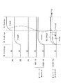
図3及び図4は、図2に示されたフラッシュメモリ装置の読み出し動作タイミング図である。
以下、メモリブロックが32本のワードラインWL0〜WL31を含むという仮定下にフラッシュメモリ装置100の読み出し動作が説明される。また、ワードラインWL0〜WL31のうちワードラインWL0〜WL15は、第1グループ、及びワードラインWL16〜WL31は、第2グループと称する。しかしながら、このような構成は、一実施形態に過ぎず、本発明で説明されるワードライングループのワードライン数及び構成は多様な形態に変更可能である。
FIG. 3 and FIG. 4 are read operation timing diagrams of the flash memory device shown in FIG.
Hereinafter, the read operation of the
図3は、第1グループWL0〜WL15に属するワードラインが選択される場合、フラッシュメモリ装置100の読み出し動作タイミング図である。図4は、第2グループWL16〜WL31に属するワードラインが選択される場合、フラッシュメモリ装置100の読み出し動作タイミング図である。
まず、図3を参照して第1グループWL0〜WL15に属するワードラインが選択される場合、フラッシュメモリ装置100の読み出し動作を説明すると、次の通りである。
FIG. 3 is a read operation timing diagram of the
First, referring to FIG. 3, when a word line belonging to the first group WL0 to WL15 is selected, a read operation of the
図3に示すように、ビットラインディスチャージ区間BL Dischargeの間ストリング選択ラインSSL、接地選択ラインGSL、共通ソースラインCSL、及びワードラインWL0〜WL31に接地電圧0Vが印加される。 As shown in FIG. 3, the ground voltage 0V is applied to the string selection line SSL, the ground selection line GSL, the common source line CSL, and the word lines WL0 to WL31 during the bit line discharge period BL Discharge.
ビットラインプリチャージ区間BL Prechargeの間、ビットラインは特定プリチャージレベルを有するようにプリチャージされる。また、図3に示すように、第2読み出し電圧Vread2が接地選択ラインGSL、第1グループWL0〜WL15及び第2グループWL16〜WL31の非選択されたワードラインに印加される。第2読み出し電圧Vread2が印加される接地選択ラインGSLは、アクティブにされる。接地電圧0Vがストリング選択ラインSSLには印加され、第1読み出し電圧Vread1が第2グループWL16〜WL31の非選択されたワードラインWL31に印加される。第1グループWL0〜WL15の選択されたワードラインには、接地電圧0Vが印加される。 During the bit line precharge period BL Precharge, the bit line is precharged to have a specific precharge level. Further, as shown in FIG. 3, the second read voltage Vread2 is applied to the unselected word lines of the ground selection line GSL, the first group WL0 to WL15, and the second group WL16 to WL31. The ground selection line GSL to which the second read voltage Vread2 is applied is activated. The ground voltage 0V is applied to the string selection line SSL, and the first read voltage Vread1 is applied to the unselected word lines WL31 of the second groups WL16 to WL31. A ground voltage of 0 V is applied to the selected word lines of the first group WL0 to WL15.
ビットラインプリチャージ区間BL Prechargeの間、接地電圧0Vがストリング選択ラインSSLに印加されるので、選択されたワードラインのセルが消去セルであっても、セルストリングは電流パスを形成しない。 Since the ground voltage 0V is applied to the string selection line SSL during the bit line precharge period BL Precharge, the cell string does not form a current path even if the cell of the selected word line is an erase cell.
ビットラインがプリチャージされる区間の間、ストリング選択ラインSSL及び接地選択ラインGSLに第2読み出し電圧Vread2が印加され、選択されたワードラインに連結されたメモリセルは、消去されたセルと仮定する。このような場合、消去されたセルは、オンセルであるので、セルストリングは電流パスを形成する。したがって、ビットラインがプリチャージされる区間の間、ストリング選択ラインSSL及び接地選択ラインGSLに第2読み出し電圧Vread2が印加されると、フラッシュメモリ装置は不必要な電力を消費する。しかしながら、前述したように、フラッシュメモリ装置100のセルストリングは、ビットラインがプリチャージされる区間の間、電流パスを形成しない。したがって、本発明のフラッシュメモリ装置100は、ビットラインがプリチャージされる区間の間、不必要な電力を消費しない。
During the period in which the bit line is precharged, the second read voltage Vread2 is applied to the string selection line SSL and the ground selection line GSL, and the memory cell connected to the selected word line is an erased cell. . In such a case, since the erased cell is an on-cell, the cell string forms a current path. Accordingly, when the second read voltage Vread2 is applied to the string selection line SSL and the ground selection line GSL during the period in which the bit line is precharged, the flash memory device consumes unnecessary power. However, as described above, the cell string of the
図3に示すように、ビットラインデベロップ区間BL Developの間、第2読み出し電圧Vread2がストリング選択ラインSSLに印加される。したがって、アクティブにされたストリング選択ラインSSLに隣接した非選択されたワードラインWL31の電圧は、ストリング選択ラインSSLに印加される電圧とのカップリング現象により上昇される。しかしながら、第1読み出し電圧Vread1は、第2読み出し電圧Vread2より低い。また、第1読み出し電圧Vread1が印加された非選択されたワードラインWL31の電圧がカップリング現象によって高まる場合、高まった第1読み出し電圧Vread1は、第2読み出し電圧Vread2より高くない。したがって、カップリング現象による非選択されたワードラインWL31に連結されたメモリセルのソフトプログラム現象が防止できる。 As shown in FIG. 3, the second read voltage Vread2 is applied to the string selection line SSL during the bit line development period BL Develop. Accordingly, the voltage of the non-selected word line WL31 adjacent to the activated string selection line SSL is raised due to a coupling phenomenon with the voltage applied to the string selection line SSL. However, the first read voltage Vread1 is lower than the second read voltage Vread2. In addition, when the voltage of the non-selected word line WL31 to which the first read voltage Vread1 is applied is increased due to the coupling phenomenon, the increased first read voltage Vread1 is not higher than the second read voltage Vread2. Therefore, the soft programming phenomenon of the memory cells connected to the non-selected word line WL31 due to the coupling phenomenon can be prevented.
接地選択ラインGSLがビットラインプリチャージ区間BL Prechargeでローレベル電圧、及びビットラインデベロップ区間BL Developで第2読み出し電圧Vread2が印加される場合、読み出し動作に問題が生まれることがある。例えば、ワードラインWL0が選択されて、ビットラインデベロップ区間BL Developで接地選択ラインGSLに第2読み出し電圧Vread2が印加される場合、カップリングによって選択されたワードラインWL0の電圧が高まる。選択されたワードラインWL0の電圧が高まる場合、正常な読み出し動作が行なわれない。したがって、選択されたワードラインが第1グループWL0〜WL15にある場合、第2読み出し電圧Vread2がビットラインプリチャージ区間BL Precharge、接地選択ラインGSLに印加される。 When the ground selection line GSL is applied with the low level voltage in the bit line precharge period BL Precharge and the second read voltage Vread2 in the bit line development period BL Develop, a problem may occur in the read operation. For example, when the word line WL0 is selected and the second read voltage Vread2 is applied to the ground selection line GSL in the bit line development period BL Develop, the voltage of the word line WL0 selected by the coupling is increased. When the voltage of the selected word line WL0 increases, normal read operation is not performed. Accordingly, when the selected word line is in the first group WL0 to WL15, the second read voltage Vread2 is applied to the bit line precharge period BL Precharge and the ground selection line GSL.
図4を参照して第2グループWL16〜WL31に属するワードラインが選択される場合、フラッシュメモリ装置100の読み出し動作を説明すると、次の通りである。
ビットラインディスチャージ区間BL Dischargeの間のタイミング図は、図3に示されたものと同様であるので、説明を省略する。
The read operation of the
The timing diagram during the bit line discharge period BL Discharge is the same as that shown in FIG.
図4に示すように、ビットラインプリチャージ区間BL Prechargeの間、図4に示すように、第2読み出し電圧Vread2がストリング選択ラインSSL、及び第1グループWL0〜WL15及び第2グループWL16〜WL31の非選択されたワードラインに印加される。第2読み出し電圧Vread2が印加されるストリング選択ラインSSLは、アクティブにされる。接地電圧0Vが接地選択ラインGSLに印加され、第1読み出し電圧Vread1が第1グループWL0〜WL15の非選択されたワードラインWL0に印加される。第2グループWL16〜WL31の選択されたワードラインには接地電圧0Vが印加される。 As shown in FIG. 4, during the bit line precharge period BL Precharge, as shown in FIG. 4, the second read voltage Vread2 is applied to the string selection line SSL, the first group WL0 to WL15, and the second groups WL16 to WL31. Applied to unselected word lines. The string selection line SSL to which the second read voltage Vread2 is applied is activated. The ground voltage 0V is applied to the ground selection line GSL, and the first read voltage Vread1 is applied to the unselected word line WL0 of the first group WL0 to WL15. A ground voltage of 0 V is applied to the selected word lines of the second group WL16 to WL31.
ビットラインプリチャージ区間BL Prechargeの間、接地電圧0Vが接地選択ラインGSLに印加されるので、選択されたワードラインのセルが消去セルであっても、セルストリングは電流パスを形成しない。したがって、本発明のフラッシュメモリ装置100は、ビットラインがプリチャージされる区間の間、不必要な電力を消費しない。
Since the ground voltage 0V is applied to the ground selection line GSL during the bit line precharge period BL Precharge, the cell string does not form a current path even if the cell of the selected word line is an erase cell. Therefore, the
図4に示すように、ビットラインデベロップ区間BL Developの間、第2読み出し電圧Vread2が接地選択ラインGSLに印加される。したがって、アクティブにされた接地選択ラインGSLに隣接した非選択されたワードラインWL0の電圧は、接地選択ラインGSLに印加される電圧とのカップリング現象によって上昇する。しかしながら、第1読み出し電圧Vread1は、第2読み出し電圧Vread2より低い。また、第1読み出し電圧Vread1が印加された非選択されたワードラインWL31の電圧がカップリング現象によって高まる場合、高まった第1読み出し電圧Vread1は第2読み出し電圧Vread2より高くない。したがって、カップリング現象による非選択されたワードラインWL0に連結されたメモリセルのソフトプログラム現象が防止できる。 As shown in FIG. 4, the second read voltage Vread2 is applied to the ground selection line GSL during the bit line development period BL Develop. Therefore, the voltage of the unselected word line WL0 adjacent to the activated ground selection line GSL rises due to a coupling phenomenon with the voltage applied to the ground selection line GSL. However, the first read voltage Vread1 is lower than the second read voltage Vread2. In addition, when the voltage of the unselected word line WL31 to which the first read voltage Vread1 is applied is increased due to a coupling phenomenon, the increased first read voltage Vread1 is not higher than the second read voltage Vread2. Therefore, the soft program phenomenon of the memory cells connected to the non-selected word line WL0 due to the coupling phenomenon can be prevented.
ストリング選択ラインSSLがビットラインプリチャージ区間BL Prechargeでローレベル電圧、そしてビットラインデベロップ区間BL Developで第2読み出し電圧Vread2が印加される場合、読み出し動作に問題が発生することがある。例えば、ワードラインWL31が選択され、ビットラインデベロップ区間BL Developでストリング選択ラインSSLに第2読み出し電圧Vread2が印加される場合、カップリングによって選択されたワードラインWL31の電圧が高まる。選択されたワードラインWL31の電圧が高まる場合、正常な読み出し動作が遂行されざるを得ない。したがって、選択されたワードラインが第2グループWL16〜WL31にある場合、第2読み出し電圧Vread2がビットラインプリチャージ区間BL Prechargeにストリング選択ラインSSLに印加される。 If the string selection line SSL is applied with a low level voltage during the bit line precharge period BL Precharge and the second read voltage Vread2 during the bit line development period BL Develop, a problem may occur in the read operation. For example, when the word line WL31 is selected and the second read voltage Vread2 is applied to the string selection line SSL in the bit line development period BL Develop, the voltage of the word line WL31 selected by the coupling is increased. When the voltage of the selected word line WL31 is increased, a normal read operation must be performed. Accordingly, when the selected word line is in the second group WL16 to WL31, the second read voltage Vread2 is applied to the string selection line SSL in the bit line precharge period BL Precharge.
結果的に、フラッシュメモリ装置は、読み出し動作モード時、デベロップ区間でストリング選択ラインに隣接したワードライン、または接地選択ラインに隣接したワードラインに連結したメモリセルに発生するソフトプログラム現象を防止できる。 As a result, the flash memory device can prevent a soft program phenomenon that occurs in a memory cell connected to a word line adjacent to a string selection line or a word line adjacent to a ground selection line in a development period in a read operation mode.
図5は、本発明の実施形態によるフラッシュメモリ装置の読み出し動作を説明するためのフローチャートである。
図5に示すように、読み出し動作モード時、ステップS1000で選択されたワードラインが第1グループWL0〜WL15及び第2グループWL16〜WL31のうち、何れに属するのか判別される。
FIG. 5 is a flowchart for explaining a read operation of the flash memory device according to the embodiment of the present invention.
As shown in FIG. 5, in the read operation mode, it is determined to which of the first groups WL0 to WL15 and the second groups WL16 to WL31 the word line selected in step S1000 belongs.
第1グループWL0〜WL15に選択されたワードラインが属する場合、ビットラインプリチャージの際、接地選択ラインGSLはアクティブにされ、前記第1読み出し電圧Vread1はストリング選択ラインにSSLすぐ隣接した非選択されたワードラインに印加される(S2000)。また、第2読み出し電圧Vread2は、第1読み出し電圧Vread1が印加された非選択されたワードラインを除外した残りの非選択されたワードラインに印加される(S2000)。以後、ビットラインデベロップの際、ストリング選択ラインSSLがアクティブにされる(S3000)。 When the selected word line belongs to the first group WL0 to WL15, the ground selection line GSL is activated during the bit line precharge, and the first read voltage Vread1 is unselected immediately adjacent to the string selection line SSL. Applied to the word line (S2000). The second read voltage Vread2 is applied to the remaining non-selected word lines excluding the non-selected word line to which the first read voltage Vread1 is applied (S2000). Thereafter, during bit line development, the string selection line SSL is activated (S3000).
第2グループWL16〜WL31に選択されたワードラインが属する場合、ビットラインプリチャージの際、ストリング選択ラインSSLはアクティブにされ、第1読み出し電圧Vread1は接地選択ラインにGSLにすぐ隣接した非選択されたワードラインに印加される(S4000)。また、第2読み出し電圧Vread2は、第1読み出し電圧Vread1が印加された非選択されたワードラインを除外した残りの非選択されたワードラインに印加される(S4000)。以後、ビットラインデベロップの際、接地選択ラインGSLがアクティブにされる(S5000) When the selected word line belongs to the second group WL16 to WL31, the string selection line SSL is activated during the bit line precharge, and the first read voltage Vread1 is not selected immediately adjacent to the ground selection line and GSL. (S4000). The second read voltage Vread2 is applied to the remaining non-selected word lines excluding the non-selected word line to which the first read voltage Vread1 is applied (S4000). Thereafter, during the bit line development, the ground selection line GSL is activated (S5000).
前述したように、第1読み出し電圧Vread1は、第2読み出し電圧Vread2より低く設定される。第1読み出し電圧Vread1が印加された非選択されたワードラインWL0またはWL31の電圧がカップリング現象によって高まる場合、高まった第1読み出し電圧Vread1は第2読み出し電圧Vread2より高くない。したがって、第1読み出し電圧Vread1がワードラインWL31またはワードラインWL0に印加されるので、ビットラインデベロップの際、ワードラインWL31またはワードラインWL0に連結されたメモリセルに発生するソフトプログラム現象が防止される。 As described above, the first read voltage Vread1 is set lower than the second read voltage Vread2. When the voltage of the unselected word line WL0 or WL31 to which the first read voltage Vread1 is applied is increased due to a coupling phenomenon, the increased first read voltage Vread1 is not higher than the second read voltage Vread2. Accordingly, since the first read voltage Vread1 is applied to the word line WL31 or the word line WL0, a soft program phenomenon that occurs in the memory cells connected to the word line WL31 or the word line WL0 during the bit line development is prevented. .
結果的に、本発明のフラッシュメモリ装置は、読み出し動作モード時、デベロップ区間でストリング選択ラインに隣接したワードラインまたは接地選択ラインに隣接したワードラインに連結されたメモリセルに発生するソフトプログラム現象を防止できる。 As a result, in the read operation mode, the flash memory device according to the present invention causes a soft program phenomenon that occurs in a memory cell connected to a word line adjacent to a string selection line or a word line adjacent to a ground selection line in a development period. Can be prevented.
図6は、本発明によるフラッシュメモリ装置を含んだコンピュータシステムを概略的に示す図である。
フラッシュメモリ装置は、電力が遮断されても保存されたデータを維持できる不揮発性メモリ装置である。セルラーフォン、PDAデジタルカメラ、ポータブルゲームコンソール、及びMP3Pのようなモバイル装置の使用増加によって、フラッシュメモリ装置は、データストレージだけでなく、コードストレージとしてより広く使用される。フラッシュメモリ装置は、また、HDTV、DVD、ルータ、及びGPSのようなホームアプリケーションに使用することができる。
FIG. 6 schematically illustrates a computer system including a flash memory device according to the present invention.
A flash memory device is a non-volatile memory device that can maintain stored data even when power is cut off. With the increasing use of mobile devices such as cellular phones, PDA digital cameras, portable game consoles, and MP3P, flash memory devices are more widely used as code storage as well as data storage. Flash memory devices can also be used for home applications such as HDTV, DVD, router, and GPS.
本発明によるフラッシュメモリ装置100を含んだコンピュータシステムが図6に概略的に示されている。本発明によるコンピュータシステムは、バス30に電気的に連結されたマイクロプロセッサ400、ユーザインタフェース500、ベースバンドチップセット(baseband chipset)のようなモデム300、フラッシュメモリコントローラ200、及びフラッシュメモリ装置100を含む。フラッシュメモリコントローラ200とフラッシュメモリ装置100とは、フラッシュメモリシステムを構成する。フラッシュメモリ装置100は、図2に示されたものと実質的に同一に構成される。フラッシュメモリ装置100には、マイクロプロセッサ400によって処理された/処理されるN-ビットデータ(Nは、1またはそれより大きい整数)がフラッシュメモリコントローラ200を通して格納される。
A computer system including a
本発明によるコンピュータシステムがモバイル装置である場合、コンピュータシステムの動作電圧を供給するためのバッテリ600が追加に提供される。ただし、図には示されなかったが、本発明によるコンピュータシステムには、応用チップセット(application chipset)、カメライメージプロセッサ(Camera Image Processor:CIS)、モバイルDRAM、などがさらに提供されることは、この分野の通常の知識を有する者に自明である。
If the computer system according to the present invention is a mobile device, an
以上、図面と明細書とで最適の実施形態が開示された。ここで特定の用語が使用されたが、これは、本発明を説明するための目的で使用されたものであり、意味限定や特許請求の範囲に記載された本発明の範囲を制限するために使用されたものではない。したがって、本技術分野の通常の知識を有する者であれば、これから多様な変形及び均等な他の実施形態が可能であることが分かる。したがって、本発明の真の技術的保護範囲は、添付された特許請求の範囲の技術的思想によって決まらなければならない。 As mentioned above, the optimal embodiment was disclosed by drawing and the specification. Certain terminology has been used herein for the purpose of describing the present invention and is intended to limit the scope of the invention as defined in the meaning and claims. It was not used. Accordingly, those having ordinary skill in the art can understand that various modifications and other equivalent embodiments are possible. Therefore, the true technical protection scope of the present invention must be determined by the technical idea of the appended claims.
10、100 フラッシュメモリ装置
20、110 メモリセルアレイ
40、120 行選択回路
60、150 ページバッファ回路
130 電圧発生回路
140 制御ロジック
200 メモリコントローラ
300 モデム
400 マイクロプロセッサ
500 ユーザインタフェース
600 バッテリ
10, 100
Claims (6)
選択されたワードラインが前記第1及び第2グループのうちの何れに属するかに従って、前記接地選択ライン及び前記ストリング選択ラインのアクティブ順序及び非選択ワードラインに印加される第1読み出し電圧及び、前記第1読み出し電圧より高い第2読み出し電圧を決定する制御ロジックと、
読み出し動作時、前記制御ロジックによって決定された結果によって、前記非選択されたワードラインを前記第1及び第2読み出し電圧で駆動し、前記接地選択ライン及び前記ストリング選択ラインをアクティブにさせる行選択回路と、を含み、
前記選択されたワードラインが前記第1グループに属する場合、前記行選択回路は前記ストリング選択ラインにすぐ隣接した非選択されたワードラインを前記第1読み出し電圧で駆動し、
前記第1読み出し電圧が印加された非選択されたワードラインを除外した残りの非選択されたワードラインを前記第2読み出し電圧で駆動し、
前記接地選択ラインはビットラインプリチャージの際アクティブにされ、前記ストリング選択ラインはビットラインデベロップの際アクティブにされ、
前記選択されたワードラインが前記第2グループに属する場合、前記行選択回路は前記接地選択ラインにすぐ隣接した非選択されたワードラインを前記第1読み出し電圧で駆動し、
前記第1読み出し電圧が印加された非選択されたワードラインを除外した残りの非選択されたワードラインを前記第2読み出し電圧で駆動し、
前記ストリング選択ラインは前記ビットラインプリチャージの際アクティブにされ、前記接地選択ラインは前記ビットラインデベロップの際アクティブにされることを特徴とするフラッシュメモリ装置。 A memory block having a word line that is separated into a first group adjacent to the ground selection line and a second group adjacent to the string selection line and arranged between the ground selection line and the string selection line ;
Depending on whether the selected word line belongs to one of said first and second group, said first read voltage is applied to the active sequence and the non-selected word line of the ground selection line and the string selection line and the Control logic for determining a second read voltage higher than the first read voltage ;
A row selection circuit that drives the non-selected word lines with the first and second read voltages and activates the ground selection line and the string selection line according to a result determined by the control logic during a read operation. and, only including,
When the selected word line belongs to the first group, the row selection circuit drives a non-selected word line immediately adjacent to the string selection line with the first read voltage;
Driving the remaining non-selected word lines excluding the non-selected word lines to which the first read voltage is applied with the second read voltage;
The ground selection line is activated during bit line precharge, the string selection line is activated during bit line development,
If the selected word line belongs to the second group, the row selection circuit drives an unselected word line immediately adjacent to the ground selection line with the first read voltage;
Driving the remaining non-selected word lines excluding the non-selected word lines to which the first read voltage is applied with the second read voltage;
The flash memory device, wherein the string selection line is activated during the bit line precharge, and the ground selection line is activated during the bit line development.
前記フラッシュメモリ装置を制御するように構成されるメモリコントローラと、を含み、
前記フラッシュメモリ装置は請求項1に記載されたフラッシュメモリ装置であることを特徴とするメモリシステム。 A flash memory device;
A memory controller configured to control the flash memory device;
The memory system according to claim 1, wherein the flash memory device is a flash memory device according to claim 1.
フラッシュメモリ装置と、
前記マイクロプロセッサからの要請に従って、前記フラッシュメモリ装置を制御するように構成されるメモリコントローラと、を含み、
前記フラッシュメモリ装置は請求項1に記載されたフラッシュメモリ装置であることを特徴とするコンピューティングシステム。 A microprocessor;
A flash memory device;
A memory controller configured to control the flash memory device according to a request from the microprocessor;
The computing system according to claim 1, wherein the flash memory device is a flash memory device according to claim 1.
前記ワードラインは接地選択ラインと隣接する第1グループと、ストリング選択ラインと隣接する第2グループとに分離され、
前記方法は、
選択されたワードラインが前記第1及び第2グループのうちの何れに属するかを判別する段階と、
前記選択されたワードラインが前記第1グループ又は前記第2グループのうち何れに属するかに従って、前記接地選択ライン及び前記ストリング選択ラインのアクティブ順序を決定する段階と、
前記接地選択ライン及び前記ストリング選択ラインのアクティブ順序及び非選択ワードラインに印加される第1読み出し電圧及び、前記第1読み出し電圧より高い第2読み出し電圧を決定する段階と、
読み出し動作時、前記第1および第2読み出し電圧が決定された結果によって、前記非選択されたワードラインを前記第1及び第2読み出し電圧で駆動し、前記接地選択ライン及び前記ストリング選択ラインのアクティブ順序を決定する段階と、
前記選択されたワードラインが前記第1グループに属する場合、前記行選択回路は前記ストリング選択ラインにすぐ隣接した非選択されたワードラインを前記第1読み出し電圧を決定する段階と、
前記行選択回路は前記第1読み出し電圧が印加された非選択されたワードラインを除外した残りの非選択されたワードラインを前記第2読み出し電圧で駆動する段階と、
前記接地選択ラインはビットラインプリチャージの際アクティブにされ、前記ストリング選択ラインはビットラインデベロップの際アクティブにされる段階とを含み、
前記選択されたワードラインが前記第2グループに属する場合、前記行選択回路は前記接地選択ラインにすぐ隣接した非選択されたワードラインを前記第1読み出し電圧で駆動する段階と、
前記行選択回路は前記第1読み出し電圧が印加された非選択されたワードラインを除外した残りの非選択されたワードラインを前記第2読み出し電圧で駆動する段階と、
前記ストリング選択ラインは前記ビットラインプリチャージの際アクティブにされ、前記接地選択ラインは前記ビットラインデベロップの際アクティブにされる段階と、を含むことを特徴とする方法。 In a reading method of a flash memory device including a memory block having a word line arranged between first and second selection lines,
The word lines are separated into a first group adjacent to the ground selection line and a second group adjacent to the string selection line;
The method
Determining which of the first and second groups the selected word line belongs to;
Determining an active order of the ground selection line and the string selection line according to whether the selected word line belongs to the first group or the second group;
Determining an active order of the ground selection line and the string selection line and a first read voltage applied to an unselected word line and a second read voltage higher than the first read voltage ;
During the read operation , the unselected word lines are driven with the first and second read voltages according to the determination result of the first and second read voltages, and the ground selection line and the string selection line are activated. Determining the order; and
If the selected word line belongs to the first group, the row selection circuit determines the first read voltage for an unselected word line immediately adjacent to the string selection line;
The row selection circuit driving the remaining non-selected word lines except the non-selected word lines to which the first read voltage is applied with the second read voltage;
The ground selection line is activated during a bit line precharge, and the string selection line is activated during a bit line development.
When the selected word line belongs to the second group, the row selection circuit drives a non-selected word line immediately adjacent to the ground selection line with the first read voltage;
The row selection circuit driving the remaining non-selected word lines except the non-selected word lines to which the first read voltage is applied with the second read voltage;
And wherein the string select line is activated during the bit line precharge, and the ground select line is activated during the bit line development .
Applications Claiming Priority (2)
| Application Number | Priority Date | Filing Date | Title |
|---|---|---|---|
| KR1020070120845A KR101416740B1 (en) | 2007-11-26 | 2007-11-26 | Flash memory device and read method thereof |
| KR10-2007-0120845 | 2007-11-26 |
Publications (3)
| Publication Number | Publication Date |
|---|---|
| JP2009129536A JP2009129536A (en) | 2009-06-11 |
| JP2009129536A5 JP2009129536A5 (en) | 2011-12-08 |
| JP5329917B2 true JP5329917B2 (en) | 2013-10-30 |
Family
ID=40669562
Family Applications (1)
| Application Number | Title | Priority Date | Filing Date |
|---|---|---|---|
| JP2008273396A Active JP5329917B2 (en) | 2007-11-26 | 2008-10-23 | Flash memory device and reading method thereof |
Country Status (3)
| Country | Link |
|---|---|
| US (1) | US7773415B2 (en) |
| JP (1) | JP5329917B2 (en) |
| KR (1) | KR101416740B1 (en) |
Families Citing this family (7)
| Publication number | Priority date | Publication date | Assignee | Title |
|---|---|---|---|---|
| KR101416740B1 (en) * | 2007-11-26 | 2014-07-09 | 삼성전자주식회사 | Flash memory device and read method thereof |
| JP5550386B2 (en) * | 2010-03-03 | 2014-07-16 | 株式会社東芝 | Nonvolatile semiconductor memory device and memory system |
| KR101692432B1 (en) * | 2010-12-23 | 2017-01-17 | 삼성전자주식회사 | Non-volatile memory device |
| KR102578153B1 (en) | 2016-08-25 | 2023-09-14 | 에스케이하이닉스 주식회사 | Memory system and operating method of the memory system |
| KR20180023190A (en) | 2016-08-25 | 2018-03-07 | 에스케이하이닉스 주식회사 | Memory system and operating method of the memory system |
| KR20200141304A (en) * | 2019-06-10 | 2020-12-18 | 에스케이하이닉스 주식회사 | Semiconductor device and operating method of semiconductor device |
| EP3915115B1 (en) * | 2019-11-28 | 2023-07-19 | Yangtze Memory Technologies Co., Ltd. | Methods of enhancing speed of reading data from memory device |
Family Cites Families (12)
| Publication number | Priority date | Publication date | Assignee | Title |
|---|---|---|---|---|
| KR960000616B1 (en) | 1993-01-13 | 1996-01-10 | 삼성전자주식회사 | Non-volatile semiconductor memory device |
| KR0169412B1 (en) | 1995-10-16 | 1999-02-01 | 김광호 | Non-volatile semiconductor memory device |
| KR0169420B1 (en) | 1995-10-17 | 1999-02-01 | 김광호 | Method of reading data on non-volatile semiconductor memory and circuit therewith |
| KR100496797B1 (en) | 1997-12-29 | 2005-09-05 | 삼성전자주식회사 | Program method of semiconductor memory device |
| JP3829088B2 (en) * | 2001-03-29 | 2006-10-04 | 株式会社東芝 | Semiconductor memory device |
| US7095653B2 (en) * | 2003-10-08 | 2006-08-22 | Micron Technology, Inc. | Common wordline flash array architecture |
| KR100632942B1 (en) | 2004-05-17 | 2006-10-12 | 삼성전자주식회사 | Program method of non-volatile memory device |
| KR100684873B1 (en) * | 2004-11-22 | 2007-02-20 | 삼성전자주식회사 | Nonvolatile memory device and word line voltage control method thereof |
| KR100680462B1 (en) | 2005-04-11 | 2007-02-08 | 주식회사 하이닉스반도체 | Non-volatile memory device and method for preventing hot electron program disturb thereof |
| JP4851779B2 (en) * | 2005-11-11 | 2012-01-11 | 株式会社東芝 | Nonvolatile semiconductor memory device and memory card equipped with the same |
| JP2008052808A (en) * | 2006-08-24 | 2008-03-06 | Toshiba Corp | Nonvolatile semiconductor memory device and method of reading data, and memory card |
| KR101416740B1 (en) * | 2007-11-26 | 2014-07-09 | 삼성전자주식회사 | Flash memory device and read method thereof |
-
2007
- 2007-11-26 KR KR1020070120845A patent/KR101416740B1/en active IP Right Grant
-
2008
- 2008-10-23 JP JP2008273396A patent/JP5329917B2/en active Active
- 2008-11-25 US US12/292,741 patent/US7773415B2/en active Active
Also Published As
| Publication number | Publication date |
|---|---|
| KR20090054125A (en) | 2009-05-29 |
| US20090135658A1 (en) | 2009-05-28 |
| KR101416740B1 (en) | 2014-07-09 |
| US7773415B2 (en) | 2010-08-10 |
| JP2009129536A (en) | 2009-06-11 |
Similar Documents
| Publication | Publication Date | Title |
|---|---|---|
| KR100890016B1 (en) | Nonvolatile memory device, memory system having its and program method thereof | |
| KR100830575B1 (en) | Flash memory device and multi-block erase method thereof | |
| JP5106817B2 (en) | Flash memory device capable of improving reliability | |
| KR100764053B1 (en) | Flash memory device and program method thereof | |
| CN102598142B (en) | Data line management in a memory device | |
| JP5275709B2 (en) | Nonvolatile memory device and program method thereof | |
| KR101391356B1 (en) | Flash memory device and read operation method thereof | |
| US7889567B2 (en) | Nonvolatile memory device for preventing program disturbance and method of programming the nonvolatile memory device | |
| KR20090010481A (en) | Nand flash memory device programming selection transistor and programming method thereof | |
| KR101462489B1 (en) | Programming method and initial charging method of nonvolatile memory device | |
| KR20100043935A (en) | Non-volatile memory device and program method thereof | |
| JP5329917B2 (en) | Flash memory device and reading method thereof | |
| KR20090002636A (en) | Nonvolatile memory device and erase method thereof | |
| US7821836B2 (en) | Flash memory device and method in which trim information is stored in memory cell array | |
| KR102416047B1 (en) | Method for controlling dummy cell and semiconduntor device | |
| JP5336053B2 (en) | Nonvolatile memory device and method of operating the same | |
| JP5329815B2 (en) | Flash memory device | |
| US10522219B2 (en) | Semiconductor memory device and method of programming multi bit data of the same | |
| JPWO2006059375A1 (en) | Semiconductor device and method for controlling semiconductor device | |
| KR101504342B1 (en) | Nonvolatile memory device, computing system and wordline driving method thereof | |
| JP4672673B2 (en) | Semiconductor device and method for controlling semiconductor device | |
| KR20090016945A (en) | Flash memory system capable of reducing read operation time and read operation method thereof | |
| JP2011028845A (en) | Semiconductor device and method of controlling semiconductor device |
Legal Events
| Date | Code | Title | Description |
|---|---|---|---|
| A521 | Request for written amendment filed |
Free format text: JAPANESE INTERMEDIATE CODE: A523 Effective date: 20111019 |
|
| A621 | Written request for application examination |
Free format text: JAPANESE INTERMEDIATE CODE: A621 Effective date: 20111019 |
|
| A131 | Notification of reasons for refusal |
Free format text: JAPANESE INTERMEDIATE CODE: A131 Effective date: 20121023 |
|
| A521 | Request for written amendment filed |
Free format text: JAPANESE INTERMEDIATE CODE: A523 Effective date: 20130116 |
|
| TRDD | Decision of grant or rejection written | ||
| A01 | Written decision to grant a patent or to grant a registration (utility model) |
Free format text: JAPANESE INTERMEDIATE CODE: A01 Effective date: 20130709 |
|
| A61 | First payment of annual fees (during grant procedure) |
Free format text: JAPANESE INTERMEDIATE CODE: A61 Effective date: 20130725 |
|
| R150 | Certificate of patent or registration of utility model |
Ref document number: 5329917 Country of ref document: JP Free format text: JAPANESE INTERMEDIATE CODE: R150 Free format text: JAPANESE INTERMEDIATE CODE: R150 |
|
| R250 | Receipt of annual fees |
Free format text: JAPANESE INTERMEDIATE CODE: R250 |
|
| R250 | Receipt of annual fees |
Free format text: JAPANESE INTERMEDIATE CODE: R250 |
|
| R250 | Receipt of annual fees |
Free format text: JAPANESE INTERMEDIATE CODE: R250 |
|
| R250 | Receipt of annual fees |
Free format text: JAPANESE INTERMEDIATE CODE: R250 |
|
| R250 | Receipt of annual fees |
Free format text: JAPANESE INTERMEDIATE CODE: R250 |
|
| R250 | Receipt of annual fees |
Free format text: JAPANESE INTERMEDIATE CODE: R250 |
|
| R250 | Receipt of annual fees |
Free format text: JAPANESE INTERMEDIATE CODE: R250 |
|
| R250 | Receipt of annual fees |
Free format text: JAPANESE INTERMEDIATE CODE: R250 |