JP5303236B2 - Optical semiconductor device - Google Patents
Optical semiconductor device Download PDFInfo
- Publication number
- JP5303236B2 JP5303236B2 JP2008256013A JP2008256013A JP5303236B2 JP 5303236 B2 JP5303236 B2 JP 5303236B2 JP 2008256013 A JP2008256013 A JP 2008256013A JP 2008256013 A JP2008256013 A JP 2008256013A JP 5303236 B2 JP5303236 B2 JP 5303236B2
- Authority
- JP
- Japan
- Prior art keywords
- quantum dot
- layer
- active layer
- density
- layers
- Prior art date
- Legal status (The legal status is an assumption and is not a legal conclusion. Google has not performed a legal analysis and makes no representation as to the accuracy of the status listed.)
- Active
Links
Images


Classifications
-
- H—ELECTRICITY
- H01—ELECTRIC ELEMENTS
- H01S—DEVICES USING THE PROCESS OF LIGHT AMPLIFICATION BY STIMULATED EMISSION OF RADIATION [LASER] TO AMPLIFY OR GENERATE LIGHT; DEVICES USING STIMULATED EMISSION OF ELECTROMAGNETIC RADIATION IN WAVE RANGES OTHER THAN OPTICAL
- H01S5/00—Semiconductor lasers
- H01S5/30—Structure or shape of the active region; Materials used for the active region
- H01S5/34—Structure or shape of the active region; Materials used for the active region comprising quantum well or superlattice structures, e.g. single quantum well [SQW] lasers, multiple quantum well [MQW] lasers or graded index separate confinement heterostructure [GRINSCH] lasers
- H01S5/341—Structures having reduced dimensionality, e.g. quantum wires
-
- B—PERFORMING OPERATIONS; TRANSPORTING
- B82—NANOTECHNOLOGY
- B82Y—SPECIFIC USES OR APPLICATIONS OF NANOSTRUCTURES; MEASUREMENT OR ANALYSIS OF NANOSTRUCTURES; MANUFACTURE OR TREATMENT OF NANOSTRUCTURES
- B82Y20/00—Nanooptics, e.g. quantum optics or photonic crystals
-
- H—ELECTRICITY
- H01—ELECTRIC ELEMENTS
- H01S—DEVICES USING THE PROCESS OF LIGHT AMPLIFICATION BY STIMULATED EMISSION OF RADIATION [LASER] TO AMPLIFY OR GENERATE LIGHT; DEVICES USING STIMULATED EMISSION OF ELECTROMAGNETIC RADIATION IN WAVE RANGES OTHER THAN OPTICAL
- H01S5/00—Semiconductor lasers
- H01S5/10—Construction or shape of the optical resonator, e.g. extended or external cavity, coupled cavities, bent-guide, varying width, thickness or composition of the active region
- H01S5/1053—Comprising an active region having a varying composition or cross-section in a specific direction
-
- H—ELECTRICITY
- H01—ELECTRIC ELEMENTS
- H01S—DEVICES USING THE PROCESS OF LIGHT AMPLIFICATION BY STIMULATED EMISSION OF RADIATION [LASER] TO AMPLIFY OR GENERATE LIGHT; DEVICES USING STIMULATED EMISSION OF ELECTROMAGNETIC RADIATION IN WAVE RANGES OTHER THAN OPTICAL
- H01S5/00—Semiconductor lasers
- H01S5/20—Structure or shape of the semiconductor body to guide the optical wave ; Confining structures perpendicular to the optical axis, e.g. index or gain guiding, stripe geometry, broad area lasers, gain tailoring, transverse or lateral reflectors, special cladding structures, MQW barrier reflection layers
- H01S5/22—Structure or shape of the semiconductor body to guide the optical wave ; Confining structures perpendicular to the optical axis, e.g. index or gain guiding, stripe geometry, broad area lasers, gain tailoring, transverse or lateral reflectors, special cladding structures, MQW barrier reflection layers having a ridge or stripe structure
-
- H—ELECTRICITY
- H01—ELECTRIC ELEMENTS
- H01S—DEVICES USING THE PROCESS OF LIGHT AMPLIFICATION BY STIMULATED EMISSION OF RADIATION [LASER] TO AMPLIFY OR GENERATE LIGHT; DEVICES USING STIMULATED EMISSION OF ELECTROMAGNETIC RADIATION IN WAVE RANGES OTHER THAN OPTICAL
- H01S5/00—Semiconductor lasers
- H01S5/30—Structure or shape of the active region; Materials used for the active region
- H01S5/34—Structure or shape of the active region; Materials used for the active region comprising quantum well or superlattice structures, e.g. single quantum well [SQW] lasers, multiple quantum well [MQW] lasers or graded index separate confinement heterostructure [GRINSCH] lasers
- H01S5/341—Structures having reduced dimensionality, e.g. quantum wires
- H01S5/3412—Structures having reduced dimensionality, e.g. quantum wires quantum box or quantum dash
Description
本発明は、光半導体装置に関し、特に活性層が複数の量子ドットを有する光半導体装置に関する。 The present invention relates to an optical semiconductor device, and more particularly to an optical semiconductor device in which an active layer has a plurality of quantum dots.
近年、複数の量子ドットを有する活性層を備えた半導体レーザや半導体光増幅器等の光半導体装置が開発されている。特許文献1には、量子ドットの形成方法が開示されている。 In recent years, optical semiconductor devices such as semiconductor lasers and semiconductor optical amplifiers having an active layer having a plurality of quantum dots have been developed. Patent Document 1 discloses a method for forming quantum dots.
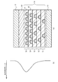
図1(a)は、従来の半導体レーザの断面模式図であり、図1(b)は、半導体レーザ内の光の導波モードを示している。図1(a)を参照に、第1導電型を有する下部クラッド層12上に活性層14が設けられている。活性層14は、量子ドット層51〜55を複数積層し備えている。量子ドット層51〜55は、複数の量子ドット41と、量子ドット41を覆うベース層40から構成される。各量子ドット層51〜55内の量子ドット密度(量子ドットの面密度)は同じである。活性層14上に第2導電型(第1導電型の反対の導電型)を有する上部クラッド層18が設けられている。
FIG. 1A is a schematic cross-sectional view of a conventional semiconductor laser, and FIG. 1B shows a waveguide mode of light in the semiconductor laser. Referring to FIG. 1A, an
下部クラッド層12と上部クラッド層18との間に電流を流すことにより、活性層14内の量子ドット41において発光し、発光した光が活性層14内を伝搬する。下部クラッド層12および上部クラッド層18の屈折率は、活性層14を主に構成するベース層40の屈折率より低い。このため、活性層14付近を伝搬する光の導波モードは図1(b)のように、活性層14の中心付近が最も大きくなる。
図1(a)に図示した光半導体レーザにおいて、素子電流を増し光出力強度を大きくするためには、量子ドット密度を高くすることが好ましい。また、半導体光増幅器において、光と電流の相互作用を増大させ光の変調効率を向上させるためには、量子ドット密度を高くすることが好ましい。しかしながら、量子ドット密度を高くすると、結晶歪が増加し非発光中心となる転位が増加してしまう。よって、発光効率や変調効率が減少してしまう。 In the optical semiconductor laser shown in FIG. 1A, it is preferable to increase the quantum dot density in order to increase the device current and increase the light output intensity. Further, in the semiconductor optical amplifier, it is preferable to increase the quantum dot density in order to increase the interaction between light and current and improve the light modulation efficiency. However, when the quantum dot density is increased, crystal distortion increases and dislocations that become non-luminescent centers increase. Therefore, the light emission efficiency and the modulation efficiency are reduced.
本発明は、上記課題に鑑みなされたものであり、量子ドットを有する光半導体装置の効率を向上させることを目的とする。 The present invention has been made in view of the above problems, and an object thereof is to improve the efficiency of an optical semiconductor device having quantum dots.
本発明は、第1導電型を有する下部クラッド層と、前記下部クラッド層上に設けられ、複数の量子ドットを有する量子ドット層が複数積層された活性層と、該活性層上に設けられ、前記第1導電型とは反対の導電型である第2導電型を有する上部クラッド層と、を具備し、前記複数の量子ドット層は、前記活性層を伝搬する光の導波モードが最も大きい量子ドット層の量子ドット密度が最も高く、各量子ドット層内の量子ドット密度は同じであることを特徴とする光半導体装置である。本発明によれば、光半導体装置の効率を向上させることができる。 The present invention includes a lower cladding layer having a first conductivity type, an active layer provided on the lower cladding layer, in which a plurality of quantum dot layers having a plurality of quantum dots are stacked, and provided on the active layer, An upper cladding layer having a second conductivity type opposite to the first conductivity type, wherein the plurality of quantum dot layers have the largest waveguide mode of light propagating through the active layer quantum dot density of the quantum dot layer is rather highest quantum dot density in the quantum dot layers is an optical semiconductor device which is a same. According to the present invention, the efficiency of the optical semiconductor device can be improved.
上記構成において、前記複数の量子ドット層は、前記活性層を伝搬する光の導波モードが最も小さい量子ドット層の量子ドット密度が最も低い構成とすることができる。この構成によれば、光の導波モードが大きさに応じ量子ドット密度を異ならせることにより、光半導体装置の効率を向上させることができる。 In the above configuration, the plurality of quantum dot layers may have a configuration in which a quantum dot layer having the smallest waveguide mode of light propagating through the active layer has the lowest quantum dot density . According to this configuration, the efficiency of the optical semiconductor device can be improved by varying the quantum dot density according to the size of the waveguide mode of light.
上記構成において、複数の量子ドット層は、最も量子ドット密度の高い量子ドット層から前記活性層の端の量子ドット層に向かい量子ドット密度が単調に減少する構成とすることができる。 In the above configuration, the plurality of quantum dot layers can be configured such that the quantum dot density monotonously decreases from the quantum dot layer having the highest quantum dot density toward the quantum dot layer at the end of the active layer.
上記構成において、前記複数の量子ドット層のうち前記活性層の中央の量子ドット層の量子ドット密度は、前記活性層の前記下部クラッド層側および前記上部クラッド層側の量子ドット層より高い構成とすることができる。 In the above configuration, the quantum dot density of the quantum dot layer in the center of the active layer among the plurality of quantum dot layers is higher than the quantum dot layers on the lower cladding layer side and the upper cladding layer side of the active layer, can do.
上記構成において、前記複数の量子ドット層のうち最上層の量子ドットの密度が最も高く、最下層の量子ドット密度が最も低い構成とすることができる。 The said structure WHEREIN: It can be set as the structure where the density of the quantum dot of the highest layer is the highest among the plurality of quantum dot layers, and the quantum dot density of the lowest layer is the lowest .
上記構成において、前記活性層上に前記下部クラッド層および前記上部クラッド層より屈折率が大きく光が伝搬する光ガイド層を具備する構成とすることができる。 The said structure WHEREIN: It can be set as the structure which comprises the light guide layer which has a refractive index larger than the said lower clad layer and the said upper clad layer, and light propagates on the said active layer.
本発明によれば、光半導体装置の効率を向上させることができる。 According to the present invention, the efficiency of the optical semiconductor device can be improved.
以下、図面を参照に本発明の実施例について説明する。 Embodiments of the present invention will be described below with reference to the drawings.
図2(a)は、実施例1に係る半導体レーザの断面模式図、図2(b)は、半導体レーザ内の光の導波モードを示している。図2(a)を参照に、光の導波モードが最も大きい中央部の量子ドット層53の量子ドット密度(量子ドットの面密度)が最も高い。一方、光の導波モードが最も小さい最上および最下の量子ドット層51、55の量子ドット密度が最も低くい。量子ドット層53から量子ドット層51、55にかけて単調に量子ドット密度が減少している。
2A is a schematic cross-sectional view of the semiconductor laser according to the first embodiment, and FIG. 2B shows a waveguide mode of light in the semiconductor laser. Referring to FIG. 2A, the quantum dot density (surface density of the quantum dots) of the
このように、複数の量子ドット層51〜55のうち活性層14の中央の量子ドット層53の量子ドット密度を活性層14の上下の量子ドット層51、55より高くする。これにより、光の導波モードが大きい活性層14の中央領域で活性層14が効率的に発光する。よって、半導体レーザの発光効率を向上させることができる。さらに、図1(a)の従来の半導体レーザと比較し、活性層14内の量子ドット41の総数をほぼ同じとすることにより、活性層14全体の結晶歪は従来と同程度とすることができる。よって、非発光中心の原因となる転位密度は従来と同程度にすることができる。
Thus, the quantum dot density of the
下部クラッド層12と上部クラッド層18の組成がほぼ同じであれば、光の導波モードは上下でほぼ対称になる。よって、量子ドット密度は上下でほぼ対称であることが好ましい。
If the compositions of the
実施例2は、最上の量子ドット層の量子ドット密度が最も高い例である。図3(a)は、実施例2に係る半導体レーザの断面模式図、図3(b)は、半導体レーザ内の光の導波モードを示している。図3(a)を参照に、実施例2においては、実施例1の図2(a)と比較し、活性層14上に光ガイド層58が設けられている。光ガイド層58は上部クラッド層18および下部クラッド層12より屈折率の大きな層である。
Example 2 is an example in which the uppermost quantum dot layer has the highest quantum dot density. FIG. 3A is a schematic cross-sectional view of a semiconductor laser according to the second embodiment, and FIG. 3B shows a waveguide mode of light in the semiconductor laser. Referring to FIG. 3A, in the second embodiment, a
光ガイド層58は光を伝搬させる機能を有している。よって、図3(b)のように、光の導波モードは、活性層14と光ガイド層58の中央付近で大きくなる。活性層14に着目すれば、活性層14の上部で光の導波モードが大きくなる。そこで、複数の量子ドット層のうち最上の量子ドット層55の量子ドット密度を最も高くする。最下の量子ドット層51の量子ドット密度を最も低くする。量子ドット層55から量子ドット層51にかけて単調に量子ドット密度を減少させる。これにより、光の導波モードが大きい活性層14の上部領域で活性層14は効率的に発光する。よって、半導体レーザの発光効率を向上させることができる。
The
実施例1および実施例2のように、前記活性層を伝搬する光の導波モードが大きい量子ドット層の量子ドット密度が高く、前記光の導波モードが小さい量子ドット層の量子ドット密度が低くなるように、複数の量子ドット層51〜55の量子ドット密度を異ならせる。これにより、半導体レーザの発光効率を向上させることができる。 As in Example 1 and Example 2, the quantum dot density of the quantum dot layer having a large waveguide mode of light propagating through the active layer is high and the quantum dot density of the quantum dot layer having a small waveguide mode of light is The quantum dot densities of the plurality of quantum dot layers 51 to 55 are made different so as to be lowered. Thereby, the light emission efficiency of the semiconductor laser can be improved.
例えば、活性層14と下部クラッド層12との間に光ガイド層が設けられ、活性層14の下部付近で光の導波モードが大きくなる場合、最下の量子ドット層51の量子ドット密度を最も高くし、最上の量子ドット層55の量子ドット密度を最も低くすることができる。
For example, when a light guide layer is provided between the
光の導波モードは一般に1つのピークを有し、上下に単調に減少する。よって、複数の量子ドット層51〜55は、最も量子ドット密度の高い量子ドット層から活性層14の端の量子ドット層51または55に向かい量子ドット密度が単調に減少することが好ましい。
The waveguide mode of light generally has one peak and decreases monotonously up and down. Therefore, it is preferable that the quantum dot layers 51 to 55 monotonically decrease from the quantum dot layer having the highest quantum dot density toward the
実施例1および実施例2では、5層の量子ドット層51〜55を例に説明したが、量子ドット層は6層以上でもよく、例えば10層以上としてもよい。量子ドットの大きさは、例えば直径が20nm程度である。量子ドット密度の大きい量子ドット層の量子ドット密度は、例えば6×10¹⁰個/cm2、量子ドット密度の小さい量子ドット層の量子ドット密度は、例えば1×1010個/cm2である。実施例1および実施例2の効果を奏するためには、量子ドット層51〜55内の最小の量子ドット密度に対し最大の量子ドット密度は、1.2倍以上であることが好ましく、1.5倍以上がより好ましい。さらに、3.0倍以上が一層好ましい。 In the first and second embodiments, the five quantum dot layers 51 to 55 have been described as examples. However, the quantum dot layer may be six layers or more, for example, ten layers or more. The size of the quantum dot is about 20 nm in diameter, for example. The quantum dot density of the quantum dot layer having a large quantum dot density is, for example, 6 × 10 10 pieces / cm 2 , and the quantum dot density of the quantum dot layer having a small quantum dot density is, for example, 1 × 10 10 pieces / cm 2 . In order to achieve the effects of Example 1 and Example 2, the maximum quantum dot density is preferably 1.2 times or more with respect to the minimum quantum dot density in the quantum dot layers 51 to 55. 5 times or more is more preferable. Furthermore, 3.0 times or more is more preferable.
実施例1および実施例2は、半導体レーザの例であったが、半導体光増幅器に実施例1および実施例2を用いてもよい。これにより、半導体光増幅器内の光と電流の相互作用を増大させ光の変調効率を向上させることができる。 Embodiments 1 and 2 are examples of semiconductor lasers, but Embodiments 1 and 2 may be used for semiconductor optical amplifiers. Thereby, the interaction between light and current in the semiconductor optical amplifier can be increased, and the light modulation efficiency can be improved.
実施例3は、実施例1および実施例2を用いた半導体レーザの例である。図4は実施例3の断面斜視図である。p型GaAs基板10上に、p型GaAsからなるバッファ層11、p型AlGaAsからな下部クラッド層12、アンドープGaAsからなるスペーサ層15、量子ドット層が複数積層した量子ドット活性層14、アンドープGaAsからなるスペーサ層16、n型AlGaAsからなる上部クラッド層18及びn型GaAsからなるコンタクト層19が順次積層されている。活性層14は、量子ドット41とベース層40とからなる。上部クラッド層18は第1層81、第2層82からなる。なお、図4では、量子ドット41の密度が量子ドット層間で同じように図示されているが、実施例1および実施例2のように、量子ドット層間で量子ドット密度が異なっている。各層の材料、膜厚及びドーピング濃度を表1に示す。

上部クラッド層18及びコンタクト層19はリッジ部30を形成している。リッジ部30の両側にはスペーサ層16に達する凹部35が形成されている。コンタクト層19上に及び凹部35表面に保護膜28として酸化シリコン膜が形成されている。リッジ部30のコンタクト層19上にn用電極22が形成されている。n用電極22と配線25を介し接続するパッド26が形成されている。基板10の下面にはp用電極24が形成されている。
The
図5は、量子ドット活性層の1層分の量子ドット層を示した図である。量子ドット41はInAsより形成される。量子ドット41間に膜厚が約5nmのInGaAs層42が形成される。量子ドット41およびInGaAs層42を覆うように、膜厚が約14nmのアンドープGaAs層43が形成される。アンドープGaAs層43上に膜厚が約10nmのp型GaAs層44、膜厚が9nmのアンドープGaAs層45が形成される。アンドープGaAs層43、p型GaAs層44、アンドープGaAs層45はベース層40を構成する。量子ドット活性層14内の各層の材料、膜厚及びドーピング濃度を表2に示す。
実施例3のように、量子ドット41としてInAs、ベース層40としてGaAs、下部クラッド層12および上部クラッド層18としてAlGaAsを用いることができる。実施例2のように光ガイド層を用いる場合、光ガイド層として例えばGaAsを用いることができる。
As in the third embodiment, InAs can be used as the
以上、発明の好ましい実施例について詳述したが、本発明は係る特定の実施例に限定されるものではなく、特許請求の範囲に記載された本発明の要旨の範囲内において、種々の変形・変更が可能である。 The preferred embodiments of the present invention have been described in detail above. However, the present invention is not limited to the specific embodiments, and various modifications and changes can be made within the scope of the gist of the present invention described in the claims. It can be changed.
10 基板
12 下部クラッド層
14 量子ドット活性層
18 上部クラッド層
40 ベース層
41 量子ドット
51〜55 量子ドット層
DESCRIPTION OF
Claims (6)
前記下部クラッド層上に設けられ、複数の量子ドットを有する量子ドット層が複数積層された活性層と、
該活性層上に設けられ、前記第1導電型とは反対の導電型である第2導電型を有する上部クラッド層と、を具備し、
前記複数の量子ドット層は、前記活性層を伝搬する光の導波モードが最も大きい量子ドット層の量子ドット密度が最も高く、
各量子ドット層内の量子ドット密度は同じであることを特徴とする光半導体装置。 A lower cladding layer having a first conductivity type;
An active layer provided on the lower cladding layer, wherein a plurality of quantum dot layers having a plurality of quantum dots are stacked;
An upper clad layer provided on the active layer and having a second conductivity type opposite to the first conductivity type;
Wherein the plurality of quantum dot layers is a quantum dot density of the guided mode is largest quantum dot layer of the propagating light is rather highest said active layer,
An optical semiconductor device characterized in that the quantum dot density in each quantum dot layer is the same .
Priority Applications (4)
| Application Number | Priority Date | Filing Date | Title |
|---|---|---|---|
| JP2008256013A JP5303236B2 (en) | 2008-10-01 | 2008-10-01 | Optical semiconductor device |
| CN2009801388365A CN102171898A (en) | 2008-10-01 | 2009-07-30 | Optical semiconductor device |
| PCT/JP2009/063598 WO2010038542A1 (en) | 2008-10-01 | 2009-07-30 | Optical semiconductor device |
| US13/121,528 US8625193B2 (en) | 2008-10-01 | 2009-07-30 | Optical semiconductor device |
Applications Claiming Priority (1)
| Application Number | Priority Date | Filing Date | Title |
|---|---|---|---|
| JP2008256013A JP5303236B2 (en) | 2008-10-01 | 2008-10-01 | Optical semiconductor device |
Publications (3)
| Publication Number | Publication Date |
|---|---|
| JP2010087325A JP2010087325A (en) | 2010-04-15 |
| JP2010087325A5 JP2010087325A5 (en) | 2011-04-21 |
| JP5303236B2 true JP5303236B2 (en) | 2013-10-02 |
Family
ID=42073319
Family Applications (1)
| Application Number | Title | Priority Date | Filing Date |
|---|---|---|---|
| JP2008256013A Active JP5303236B2 (en) | 2008-10-01 | 2008-10-01 | Optical semiconductor device |
Country Status (4)
| Country | Link |
|---|---|
| US (1) | US8625193B2 (en) |
| JP (1) | JP5303236B2 (en) |
| CN (1) | CN102171898A (en) |
| WO (1) | WO2010038542A1 (en) |
Families Citing this family (3)
| Publication number | Priority date | Publication date | Assignee | Title |
|---|---|---|---|---|
| JP6601791B2 (en) * | 2015-07-13 | 2019-11-06 | 株式会社Qdレーザ | Semiconductor laser, optical module, optical communication device, and optical communication system |
| US10840676B2 (en) * | 2018-05-10 | 2020-11-17 | X Development Llc | Optoelectronic devices having spatially varying distribution of quantum confined nanostructures |
| JP2022078795A (en) * | 2020-11-13 | 2022-05-25 | 株式会社デンソー | Semiconductor laser device |
Family Cites Families (11)
| Publication number | Priority date | Publication date | Assignee | Title |
|---|---|---|---|---|
| JP3236325B2 (en) | 1991-11-19 | 2001-12-10 | 富士通株式会社 | Semiconductor light emitting device |
| JP3468866B2 (en) | 1994-09-16 | 2003-11-17 | 富士通株式会社 | Semiconductor device using three-dimensional quantum confinement |
| JP3008927B2 (en) * | 1998-04-17 | 2000-02-14 | 日本電気株式会社 | Semiconductor laser and semiconductor optical amplifier |
| JP2001210910A (en) * | 1999-11-17 | 2001-08-03 | Mitsubishi Electric Corp | Semiconductor laser |
| JP4006729B2 (en) | 2002-04-16 | 2007-11-14 | 富士通株式会社 | Semiconductor light-emitting device using self-assembled quantum dots |
| WO2004055900A1 (en) | 2002-12-16 | 2004-07-01 | Japan Science And Technology Agency | Semiconductor multilayer structure having inhomogeneous quantum dots, light-emitting diode using same, semiconductor laser diode, semiconductor optical amplifier, and method for manufacturing them |
| JP2004289010A (en) | 2003-03-24 | 2004-10-14 | Sony Corp | Light emitting device |
| JP2005039107A (en) * | 2003-07-17 | 2005-02-10 | Sharp Corp | Oxide semiconductor laser element |
| JP4822244B2 (en) * | 2004-03-19 | 2011-11-24 | 富士通株式会社 | Semiconductor light-emitting device using self-forming quantum dots |
| JP2008098299A (en) * | 2006-10-10 | 2008-04-24 | Mitsubishi Electric Corp | Semiconductor optical device and manufacturing method thereof |
| JP5145183B2 (en) | 2008-09-26 | 2013-02-13 | 日本電産サンキョー株式会社 | Door lock device |
-
2008
- 2008-10-01 JP JP2008256013A patent/JP5303236B2/en active Active
-
2009
- 2009-07-30 WO PCT/JP2009/063598 patent/WO2010038542A1/en active Application Filing
- 2009-07-30 US US13/121,528 patent/US8625193B2/en not_active Expired - Fee Related
- 2009-07-30 CN CN2009801388365A patent/CN102171898A/en active Pending
Also Published As
| Publication number | Publication date |
|---|---|
| US8625193B2 (en) | 2014-01-07 |
| WO2010038542A1 (en) | 2010-04-08 |
| JP2010087325A (en) | 2010-04-15 |
| US20110181945A1 (en) | 2011-07-28 |
| CN102171898A (en) | 2011-08-31 |
Similar Documents
| Publication | Publication Date | Title |
|---|---|---|
| US7693361B2 (en) | Hybrid laser diode | |
| JP4869580B2 (en) | Single mode vertical cavity surface emitting laser and method of manufacturing the same | |
| JP2007251174A (en) | Vcsel semiconductor device accompanying modal control | |
| JP4483615B2 (en) | Epitaxial wafer for semiconductor light emitting device and semiconductor light emitting device | |
| CN1732604A (en) | Distributed Bragg reflector for optoelectronic device | |
| EP1999827A2 (en) | Red light laser | |
| JP2007173802A (en) | Manufacturing method of single mode vcsel for optical mouse | |
| WO2007116659A1 (en) | Surface light-emitting laser | |
| TWI607612B (en) | Semiconductor laser device | |
| JP5303236B2 (en) | Optical semiconductor device | |
| JP6581024B2 (en) | Distributed feedback laser diode | |
| JP2006128617A (en) | Semiconductor laser element and its manufacturing method | |
| JP5379002B2 (en) | Semiconductor laser and manufacturing method thereof | |
| JP6807691B2 (en) | Semiconductor optical device and its manufacturing method | |
| JP2007311632A (en) | Surface-emitting laser element | |
| JP2022140943A (en) | Semiconductor light-emitting device and optical coupling device | |
| JP5224155B2 (en) | Surface emitting laser element, surface emitting laser array including the same, image forming apparatus including surface emitting laser array, surface pickup laser element or optical pickup apparatus including surface emitting laser array, surface emitting laser element or surface emitting laser array An optical transmission module comprising: an optical transmission / reception module comprising a surface emitting laser element or a surface emitting laser array; and an optical communication system comprising a surface emitting laser element or a surface emitting laser array. | |
| JP5188259B2 (en) | Light emitting device using three-dimensional photonic crystal | |
| JP2006120884A (en) | Semiconductor light emitting device, surface-emission laser, surface-emission laser array, image forming apparatus, optical pickup system, optical transmission module, optical transceiving module, and optical communication system | |
| JP5840893B2 (en) | Semiconductor laser device | |
| US20240030685A1 (en) | Semiconductor laser diode | |
| WO1997033351A1 (en) | Semiconductor laser | |
| US20230020718A1 (en) | Vcsel with increased wavelength dependence on driving current | |
| JP7172182B2 (en) | Light emitting device, optical signal transmitter and optical transmission system | |
| CN117424068A (en) | Semiconductor laser diode |
Legal Events
| Date | Code | Title | Description |
|---|---|---|---|
| A521 | Request for written amendment filed |
Free format text: JAPANESE INTERMEDIATE CODE: A523 Effective date: 20110307 |
|
| A621 | Written request for application examination |
Free format text: JAPANESE INTERMEDIATE CODE: A621 Effective date: 20110307 |
|
| A131 | Notification of reasons for refusal |
Free format text: JAPANESE INTERMEDIATE CODE: A131 Effective date: 20121211 |
|
| TRDD | Decision of grant or rejection written | ||
| A01 | Written decision to grant a patent or to grant a registration (utility model) |
Free format text: JAPANESE INTERMEDIATE CODE: A01 Effective date: 20130528 |
|
| A61 | First payment of annual fees (during grant procedure) |
Free format text: JAPANESE INTERMEDIATE CODE: A61 Effective date: 20130624 |
|
| R150 | Certificate of patent or registration of utility model |
Ref document number: 5303236 Country of ref document: JP Free format text: JAPANESE INTERMEDIATE CODE: R150 Free format text: JAPANESE INTERMEDIATE CODE: R150 |
|
| R250 | Receipt of annual fees |
Free format text: JAPANESE INTERMEDIATE CODE: R250 |
|
| R250 | Receipt of annual fees |
Free format text: JAPANESE INTERMEDIATE CODE: R250 |
|
| R250 | Receipt of annual fees |
Free format text: JAPANESE INTERMEDIATE CODE: R250 |
|
| R250 | Receipt of annual fees |
Free format text: JAPANESE INTERMEDIATE CODE: R250 |
|
| R250 | Receipt of annual fees |
Free format text: JAPANESE INTERMEDIATE CODE: R250 |
|
| R250 | Receipt of annual fees |
Free format text: JAPANESE INTERMEDIATE CODE: R250 |
|
| R250 | Receipt of annual fees |
Free format text: JAPANESE INTERMEDIATE CODE: R250 |
|
| R250 | Receipt of annual fees |
Free format text: JAPANESE INTERMEDIATE CODE: R250 |