JP5295286B2 - Storage device and computer equipped with the same - Google Patents
Storage device and computer equipped with the same Download PDFInfo
- Publication number
- JP5295286B2 JP5295286B2 JP2011036717A JP2011036717A JP5295286B2 JP 5295286 B2 JP5295286 B2 JP 5295286B2 JP 2011036717 A JP2011036717 A JP 2011036717A JP 2011036717 A JP2011036717 A JP 2011036717A JP 5295286 B2 JP5295286 B2 JP 5295286B2
- Authority
- JP
- Japan
- Prior art keywords
- conversion table
- cache
- logical
- block
- physical address
- Prior art date
- Legal status (The legal status is an assumption and is not a legal conclusion. Google has not performed a legal analysis and makes no representation as to the accuracy of the status listed.)
- Expired - Fee Related
Links
- 230000015654 memory Effects 0.000 claims abstract description 107
- 238000012545 processing Methods 0.000 claims abstract description 69
- 238000013519 translation Methods 0.000 claims abstract description 22
- 238000006243 chemical reaction Methods 0.000 claims description 193
- 238000007726 management method Methods 0.000 claims description 132
- 238000000034 method Methods 0.000 claims description 73
- 230000008569 process Effects 0.000 claims description 58
- 238000005192 partition Methods 0.000 claims description 16
- 238000013523 data management Methods 0.000 claims description 3
- 238000013500 data storage Methods 0.000 claims 1
- 238000000638 solvent extraction Methods 0.000 abstract 1
- 238000010586 diagram Methods 0.000 description 19
- 230000006870 function Effects 0.000 description 4
- 230000001174 ascending effect Effects 0.000 description 2
- 238000012790 confirmation Methods 0.000 description 2
- 239000004065 semiconductor Substances 0.000 description 2
- 230000002950 deficient Effects 0.000 description 1
- 230000000694 effects Effects 0.000 description 1
- 238000012986 modification Methods 0.000 description 1
- 230000004048 modification Effects 0.000 description 1
- 230000009467 reduction Effects 0.000 description 1
- 230000004044 response Effects 0.000 description 1
- 230000011218 segmentation Effects 0.000 description 1
- 230000003068 static effect Effects 0.000 description 1
- 230000007704 transition Effects 0.000 description 1
Images


Classifications
-
- G—PHYSICS
- G06—COMPUTING; CALCULATING OR COUNTING
- G06F—ELECTRIC DIGITAL DATA PROCESSING
- G06F12/00—Accessing, addressing or allocating within memory systems or architectures
- G06F12/02—Addressing or allocation; Relocation
- G06F12/0223—User address space allocation, e.g. contiguous or non contiguous base addressing
- G06F12/023—Free address space management
- G06F12/0238—Memory management in non-volatile memory, e.g. resistive RAM or ferroelectric memory
- G06F12/0246—Memory management in non-volatile memory, e.g. resistive RAM or ferroelectric memory in block erasable memory, e.g. flash memory
-
- G—PHYSICS
- G06—COMPUTING; CALCULATING OR COUNTING
- G06F—ELECTRIC DIGITAL DATA PROCESSING
- G06F12/00—Accessing, addressing or allocating within memory systems or architectures
- G06F12/02—Addressing or allocation; Relocation
- G06F12/08—Addressing or allocation; Relocation in hierarchically structured memory systems, e.g. virtual memory systems
- G06F12/10—Address translation
- G06F12/1027—Address translation using associative or pseudo-associative address translation means, e.g. translation look-aside buffer [TLB]
-
- G—PHYSICS
- G06—COMPUTING; CALCULATING OR COUNTING
- G06F—ELECTRIC DIGITAL DATA PROCESSING
- G06F2212/00—Indexing scheme relating to accessing, addressing or allocation within memory systems or architectures
- G06F2212/72—Details relating to flash memory management
- G06F2212/7201—Logical to physical mapping or translation of blocks or pages
Abstract
Description
本発明は、記憶装置およびそれを搭載した計算機に関する。 The present invention relates to a storage device and a computer equipped with the storage device.
情報機器の補助記憶装置として、一般には磁気ディスク記憶装置が用いられている。この磁気ディスク記憶装置では、データの読み出し及び書き込みはセクタと呼ばれる記憶単位ごとに行われている。 Generally, a magnetic disk storage device is used as an auxiliary storage device for information equipment. In this magnetic disk storage device, data reading and writing are performed for each storage unit called a sector.
近年、上記のような磁気ディスク記憶装置に代わり、半導体メモリを記憶媒体とする記憶装置が増えてきている。その中でも、電気的に消去可能かつ再書き込み可能な不揮発性メモリEEPROM(Electrically Erasable Programmable Read only Memory)の一種であるフラッシュメモリを用いた記憶装置が主流となってきている。 In recent years, an increasing number of storage devices using a semiconductor memory as a storage medium in place of the magnetic disk storage device as described above. Among them, a storage device using a flash memory which is a kind of electrically erasable and rewritable nonvolatile memory EEPROM (Electrically Erasable Programmable Read Only Memory) has become mainstream.
このフラッシュメモリは、磁気ディスクと比べて読み出し及び書き込み速度に優れるが、使用上の制限が4つ存在する。1つ目は、データの読み出し及び書き込み単位(一般にページと呼ばれる)と消去単位(一般にブロックと呼ばれ、複数のページから構成される)が決まっており、ブロックはページよりもサイズが大きいことである。2つ目は、データを上書きする際には、1度データを消去した後に、再度書き込みを行う必要があることである。3つ目は、ブロック内のあるページにデータを書き込む場合、連続したページ番号順に書き込む必要があることである。4つ目は、ブロックごとに消去回数の上限が決まっていることである。 Although this flash memory is superior in reading and writing speed as compared with a magnetic disk, there are four restrictions in use. The first is that the unit for reading and writing data (generally called a page) and the unit for erasing (generally called a block, consisting of a plurality of pages) are determined, and the block is larger in size than the page. is there. Second, when data is overwritten, it is necessary to write again after erasing the data once. Third, when data is written to a certain page in the block, it is necessary to write in the order of consecutive page numbers. The fourth is that the upper limit of the number of times of erasure is determined for each block.
特許文献1では、上記のフラッシュメモリ特性を考慮し、記憶装置の高性能化および長寿命化を行うためのメモリ制御方法を提案している。ここでは、「不揮発性半導体メモリを管理する際に、物理ブロックをスクラッチブロック、データブロック、消去済みブロックの3種類に分けている。ホスト装置からのデータ書き込みは、スクラッチブロックに対して行う。スクラッチブロック内の空きページが無くなった場合には、このブロックを以降はデータブロックとして扱い、消去済みブロックの中から1つを新たにスクラッチブロックとして割り当てる。また、消去済みブロックが不足した場合は、データブロックの中から有効なデータの少ないブロックを選択し、当該ブロックに含まれるすべての有効なデータをスクラッチブロックにコピーした後、ブロック消去を行い、消去済みブロックを得る。」としている。
また、特許文献2には、記憶装置に搭載するRAM容量を抑えるための方法が提案されている。ここでは、「揮発性記憶手段に記憶される第1のアドレス変換テーブル、不揮発性記憶手段に記憶される第2のアドレス変換テーブルを備える。受信された要求に係る論理セクタアドレスと揮発性記憶手段によって記憶された第1のアドレス変換テーブルとから、不揮発性記憶手段に記憶される第2のアドレス変換テーブルの物理ロケーションを取得する。第1のアドレス取得手段によって取得された物理ロケーションに基づいて、不揮発性記憶手段に記憶された第2のアドレス変換テーブルを得る。受信手段によって受信された要求に係る論理セクタアドレスと当該第2のアドレス変換テーブルとから、不揮発性記憶手段に対しデータを書き込む。」としている。
Patent Document 2 proposes a method for suppressing the capacity of a RAM mounted on a storage device. Here, “the first address conversion table stored in the volatile storage means and the second address conversion table stored in the nonvolatile storage means are provided. The logical sector address and the volatile storage means related to the received request. To obtain the physical location of the second address translation table stored in the non-volatile storage means from the first address translation table stored in the
また、特許文献3には、ホスト計算機からの書き込み要求に対する応答速度を速める方法が提案されている。ここでは、「WC(ライトキャッシュ)追い出し制御部は、WCリソース使用量を上限値Clmtより値が小さいAF(Auto Flush)閾値Cafと比較する。WCリソース使用量がAF閾値Cafを越えているときは、NANDメモリでの整理の状態を確認する。NANDメモリでの整理が充分に進んでいる場合には、早めにWCからNANDメモリにデータを追い出す。」としている。 Patent Document 3 proposes a method of increasing the response speed to a write request from a host computer. In this case, “the WC (write cache) eviction control unit compares the WC resource usage amount with an AF (Auto Flush) threshold value Caf that is smaller than the upper limit value Clmt. When the WC resource usage amount exceeds the AF threshold value Caf Confirms the state of arrangement in the NAND memory. If the arrangement in the NAND memory is sufficiently advanced, the data is expelled from the WC to the NAND memory as soon as possible.
特許文献1には、ページ単位でデータ構造を管理するメモリ制御方式が記載されている。このメモリ制御方式は、データをページ単位で管理するために高速な処理が可能であるが、ブロック単位で管理する方法に比べて論理/物理アドレス変換テーブルの容量が大きくなる。しかも、この論理/物理アドレス変換テーブルは記憶装置の記憶容量に比例して増加する。そのため、記憶装置の大容量化を行うと、論理/物理アドレス変換テーブルを格納するための大容量メモリが必要となり、記憶装置の大型化やコストの増大につながるという問題がある。
特許文献2では、論理/物理アドレス変換テーブルをRAMとフラッシュメモリに分割して保存することで、RAM容量を削減する方法が記載されている。この方法によれば、特許文献1で課題としたRAM容量の大幅削減を可能とするが、計算機からの書き込み処理に対して、テーブル情報とデータの2ページ分の書き込みが発生してしまう。そのため、テーブル情報を書き込まない場合と比べて処理速度が低下し、フラッシュメモリの書き換え回数を消耗するという問題がある。
Patent Document 2 describes a method of reducing the RAM capacity by dividing a logical / physical address conversion table into a RAM and a flash memory and storing them. According to this method, it is possible to drastically reduce the RAM capacity, which is a problem in
上記課題を解決するために、不揮発性メモリに論理/物理アドレス変換テーブルを保存し、RAMには論理/物理アドレス変換テーブルの一部をキャッシュとして保持することで、RAM容量を削減しつつ、処理速度の低下を抑制する方法が考えられる。 In order to solve the above problems, a logical / physical address conversion table is stored in a non-volatile memory, and a part of the logical / physical address conversion table is stored as a cache in the RAM, thereby reducing the RAM capacity and processing. A method for suppressing the decrease in speed is conceivable.
このようなキャッシュを用いたデータ管理方法の一例が、特許文献3に記載されたWC(ライトキャッシュ)とNANDフラッシュメモリ間でのデータ制御方法である。 One example of a data management method using such a cache is a data control method between a WC (write cache) and a NAND flash memory described in Patent Document 3.
このデータ制御方法では、WC内のデータ管理情報として、WCトラック情報を使用している。WCトラック情報は、キャッシュ内に保持しているトラックのアドレスやトラック内の有効セクタ数などの情報を有しているが、キャッシュのエントリ分の情報しか保持していない。同様のキャッシュ管理情報を論理/物理アドレス変換テーブル情報のキャッシュ管理に適応したとしても、キャッシュに保持されていないテーブル情報が不揮発性メモリ内のどの物理アドレスに保存されているか把握できないと言う問題がある。 In this data control method, WC track information is used as data management information in the WC. The WC track information includes information such as the address of the track held in the cache and the number of valid sectors in the track, but holds only the information for the cache entry. Even if the same cache management information is applied to the cache management of the logical / physical address conversion table information, there is a problem that it is not possible to grasp at which physical address in the nonvolatile memory the table information not held in the cache is stored. is there.
そこで、本発明では、記憶装置の大型化やコストの増大を阻止しながら、処理速度が低下せず、かつ不揮発性メモリ内の物理アドレス管理を可能とする記憶装置およびそれを搭載した計算機を提供することを目的とする。 In view of this, the present invention provides a storage device capable of managing the physical address in the nonvolatile memory without reducing the processing speed while preventing an increase in the size and cost of the storage device, and a computer equipped with the storage device. The purpose is to do.
上記課題を解決するために、本発明では不揮発性メモリに論理/物理アドレス変換テーブルを保存し、RAMには論理/物理アドレス変換テーブルの一部をキャッシュとして保持することで、RAM容量を削減しつつ、処理速度の低下を抑制する。また、キャッシュに保持されていないテーブル情報が不揮発性メモリのどこに保持されているかを管理し、テーブル情報がキャッシュに保持されているか否かを識別する情報を有することで、論理/物理アドレス変換テーブルのキャッシュ管理を実現する。 In order to solve the above problems, in the present invention, a logical / physical address conversion table is stored in a nonvolatile memory, and a part of the logical / physical address conversion table is stored as a cache in the RAM, thereby reducing the RAM capacity. However, a reduction in processing speed is suppressed. In addition, the logical / physical address conversion table has information for managing where the table information not held in the cache is held in the nonvolatile memory and identifying whether the table information is held in the cache. Cache management is realized.
本願は上記課題を解決する手段を複数含んでいるが、その一例を挙げるならば、ある所定の書き込み単位であるページ2220と前記書き込み単位よりも大きいデータ消去単位であるブロック222を持つ不揮発性メモリ22と、データの読み出し及び書き込みが出来るRAM23と、前記不揮発性メモリ22および前記RAM23への読み出し及び書き込み処理を行うメモリコントローラ21を有する記憶装置2であって、
前記不揮発性メモリ22は、命令処理装置4が書き込みを行ったデータ221と、前記データ221の格納場所を管理する論理/物理アドレス変換テーブル220を前記ページ2220単位に分割した複数の分割変換テーブル240を有し、
前記RAM23は、前記分割変換テーブル240の少なくとも1つ以上を保存する論理/物理アドレス変換テーブルキャッシュ230と、前記分割変換テーブル240を管理する変換テーブル管理テーブル235と、前記論理/物理アドレス変換テーブルキャッシュ230の管理を行うキャッシュ管理テーブル236を有し、
前記変換テーブル管理テーブル235は、前記分割変換テーブルが前記論理/物理アドレス変換テーブルキャッシュ230に保存されていることを示すキャッシュ有無フラグ2352と、前記論理/物理アドレス変換テーブルキャッシュ230における前記分割変換テーブル240の保存先を示すキャッシュエントリ番号2355を有し、
前記不揮発性メモリ22と前記RAM23の間における前記論理/物理アドレス変換テーブル220の情報の読み出し及び書き込みは、前記ページ2220単位で行うことを特徴とする。
The present application includes a plurality of means for solving the above-described problem. For example, a nonvolatile memory having a
The
The
The conversion table management table 235 includes a
Reading and writing of information in the logical / physical address conversion table 220 between the
本発明によれば、論理/物理アドレス変換テーブルを不揮発性メモリ内に保存し、RAMには論理/物理アドレス変換テーブルの必要とする一部分のみを保持することで、RAM容量を削減することができる。また、RAMに保持した論理/物理アドレス変換テーブルをキャッシュとして使用することで、不揮発性メモリに対する論理/物理アドレス変換テーブル情報の書き込み回数を削減させ、処理速度の低下を抑制することができる。 According to the present invention, the logical / physical address conversion table is stored in the non-volatile memory, and the RAM capacity can be reduced by holding only a required part of the logical / physical address conversion table in the RAM. . In addition, by using the logical / physical address conversion table held in the RAM as a cache, the number of times of writing logical / physical address conversion table information to the nonvolatile memory can be reduced, and a decrease in processing speed can be suppressed.
上記した以外の課題、構成及び効果は、以下の実施形態の説明により明らかにされる。 Problems, configurations, and effects other than those described above will be clarified by the following description of embodiments.
以下、図面を用いて本発明の実施例を説明する。 Embodiments of the present invention will be described below with reference to the drawings.
図1は本実施例におけるハードウェア構成の例である。図1に示す計算機1は、記憶装置2、命令処理装置4、主記憶メモリ5、入出力制御装置6、ネットワーク制御装置7、表示装置8を持ち、各装置は相互にデータバス3によって接続されている。
FIG. 1 is an example of a hardware configuration in this embodiment. A
これらのうち、記憶装置2は、命令処理装置4からの処理に従い、データの読み出し及び書き込みを行う。 Among these, the storage device 2 reads and writes data according to the processing from the instruction processing device 4.
命令処理装置4は、記憶装置2もしくは主記憶メモリ5に格納されている命令を処理し、記憶装置2および主記憶メモリ5に対するデータの読み出し及び書き込みや、入出力制御装置6、ネットワーク制御装置7、表示装置8に対する処理を行う。 The instruction processing device 4 processes instructions stored in the storage device 2 or the main storage memory 5, reads / writes data from / to the storage device 2 and the main storage memory 5, an input / output control device 6, a network control device 7. Then, the display device 8 is processed.
主記憶メモリ5は、命令処理装置4からの処理に従い、データの読み出し及び書き込みを行う。 The main memory 5 reads and writes data according to processing from the instruction processing device 4.
入出力制御装置6は、外部機器(図示せず)とデータバス3間でのデータの入出力を制御する装置である。この外部機器の例としては、キーボードやマウス、あるいは外付けの記憶装置2などが挙げられる。 The input / output control device 6 is a device that controls input / output of data between an external device (not shown) and the data bus 3. Examples of the external device include a keyboard, a mouse, and an external storage device 2.
ネットワーク制御装置7は、ネットワーク(図示せず)とデータバス3間でのデータの入出力を制御する装置である。 The network control device 7 is a device that controls input / output of data between a network (not shown) and the data bus 3.
表示装置8は、命令処理装置4からの処理に従い、データの表示などを行う装置である。 The display device 8 is a device that displays data in accordance with processing from the instruction processing device 4.
記憶装置2は、I/F(インターフェース)制御部20、メモリコントローラ21、1つ以上の不揮発性メモリ22、およびRAM23から構成される。
The storage device 2 includes an I / F (interface)
I/F制御部20は、命令処理装置4とメモリコントローラ21間のデータの制御を行う。メモリコントローラ21は、命令処理装置4からの命令に従い、不揮発性メモリ22内のデータの読み出し及び書き込みを行い、それに付随してRAM23内のデータ更新を行う。
The I /
不揮発性メモリ22には、論理/物理アドレス変換テーブル220、およびデータ221を格納する。本実施例で記載の不揮発性メモリ22とは、所定の書き込み単位(ページ)と書き込み単位より大きい消去単位(ブロック)を持ち、データを書き換える場合には、書き込みの前に消去動作を必要とする不揮発性メモリを指す。なお、不揮発性メモリ22の内容については、図2、図3を用いて詳細に後述する。また、論理/物理アドレス変換テーブル220の一例が図6に示されている。
The
RAM23には、論理/物理アドレス変換テーブルキャッシュ230、スクラッチブロック管理テーブル231(図7)、データブロック管理テーブル232(図8)、消去済みブロック管理テーブル233(図9)、物理ブロック管理テーブル234(図10)、変換テーブル管理テーブル235(図11)、キャッシュ管理テーブル236(図12)を格納する。
The
なお、RAM23内に保持する論理/物理アドレス変換テーブルキャッシュ230は、不揮発性メモリ22に保存している論理/物理アドレス変換テーブル220の一部を保存するものである。
The logical / physical address
このRAM23は、MRAM(Magnetic RAM)のような不揮発性メモリであっても、SRAM(Static RAM)やDRAM(Dynamic RAM)のような揮発性メモリであってもよい。ただし、不揮発性メモリを用いる場合には、データ書き換え時に消去動作を必要としない不揮発性メモリである必要がある。また、このRAM23はメモリコントローラ21の内部にあってもよい。
The
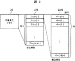
図2は、不揮発性メモリ22の内部構成を示した図である。不揮発性メモリは1つ以上の消去単位から構成され、この消去単位をブロック222と呼ぶ。また、このブロック222は1つ以上の書き込み単位から構成され、これをページ2220と呼ぶ。本実施例では、不揮発性メモリ22のブロック(222)数はMブロック、1ブロック当たりのページ(2220)数はNページとして扱う。なお、ページ2220の種類と構成が図5に示されており、後述する。
FIG. 2 is a diagram showing an internal configuration of the
図3は、本実施例における不揮発性メモリ22の使用状態を示した図である。本実施例では、ブロック222をスクラッチブロック群223、データブロック群224、消去済みブロック群225の3つのグループのいずれかに分類して使用する。従って、スクラッチブロック群223、データブロック群224、消去済みブロック群225の3つのグループの合計ブロック数は、M個である。
FIG. 3 is a diagram showing a usage state of the
スクラッチブロック群223は、1つ以上のスクラッチブロック2230から構成される。スクラッチブロック2230は、ブロックヘッダページ2221、データページ2222、テーブルページ2223、空きページ2224から構成される。ただし、データページ2222もしくはテーブルページ2223のどちらかを有していないこともある。
The
データブロック群224は、1つ以上のデータブロック2240から構成される。データブロック2240は、ブロックヘッダページ2221、データページ2222、テーブルページ2223から構成される。ただし、スクラッチブロック2230と同様に、データページ2222もしくはテーブルページ2223のどちらかを有していないこともある。データブロック2240は、スクラッチブロック2230とは異なり、空きページ2224を有していない。
The
消去済みブロック群225は、1つ以上の消去済みブロック2250から構成される。消去済みブロック2250は、ブロックヘッダページ2221と空きページ2224から構成され、データページ2222およびテーブルページ2223は保有しない。
The erased
図4は、ブロックとページの関係を纏めた図である。横方向にスクラッチブロック2230、データブロック2240、消去済みブロック2250の各ブロックを記載し、縦方向にブロックヘッダページ2221、データページ2222、テーブルページ2223、空きページ2224の各ページを記載している。この図で、○は、当該ページを備えることを意味し、×は当該ページを備えないことを意味する。また、△は当該ページのいずれかを備えないことがあることを意味している。なお、ブロックヘッダページ2221、データページ2222、テーブルページ2223の構成については、図5a,図5b、図5cに示されている。
FIG. 4 is a diagram summarizing the relationship between blocks and pages. Each block of the
不揮発性メモリ22内のブロック222は、上記3グループのいずれかに所属し、データ書き込みやブロック消去の処理によって、その所属を動的に移行していく。つまり、例えば特許文献1に示すように、スクラッチブロックがデータブロックに移行し、消去済みブロックの一部を新たにスクラッチブロックに割り当て、データブロックを消去済みブロックに移行するといった具合に、所属の動的移行を行う。
The
また、図1における論理/物理アドレス変換テーブル220は、実際にはテーブルページ2223のようにページ単位に分割して保存される形となる。
In addition, the logical / physical address conversion table 220 in FIG. 1 is actually stored in a divided page unit like a
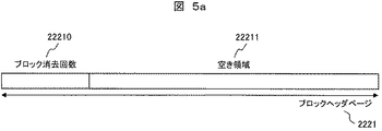
図5は、ページ2220に格納するデータ構造を示した図である。図3で説明したように、ここには3種類のデータ構造がある。ブロックヘッダページ2221と、データページ2222と、テーブルページ2223である。
FIG. 5 is a diagram illustrating a data structure stored in the
このうち、ブロックヘッダページ2221内には、図5aに示すように、少なくともブロック消去回数22210の情報を格納する。空き領域22211は、情報を書き込まない領域であるが、この部分に不良ブロックを表すフラグやエラー発生回数の情報を格納してもよい。
Among these, in the
データページ2222は、図5bに示すように、データページヘッダ情報22220とデータ22221を有する。データページヘッダ情報22220は、ページ属性22222、論理アドレス22223、データ書き込み番号22224を含む。
The
ページ属性22222には、このページがデータページ2222であるのか、テーブルページ2223であるのかを判別する際に使用するフラグを格納する。論理アドレス22223には、命令処理装置4が付与した論理アドレス情報を格納する。データ書き込み番号22224は、論理アドレス番号22223が同一であるデータページ2222が複数存在した場合に、データ22221の新旧を判別するために使用する番号である。
The
本来ならば、データ22221の新旧は後述する各種の管理テーブルによって管理されるため、データ書き込み番号22224は必須ではない。しかし、データ書き込み番号22224があると、何らかの原因によってRAM内のテーブル情報が破壊された場合でも復旧可能となるため、本実施例では記載している。
Originally, since the new and
テーブルページ2223は、図5cに示すように、テーブルページヘッダ情報22230と論理/物理アドレス変換テーブル値22231を有する。テーブルページヘッダ情報22230は、ページ属性22232、テーブル管理番号22233、テーブル書き込み番号22234を含む。このうち、ページ属性22232は、図5bのデータページ2222におけるページ属性22222と同じ機能のものであり、ここでの説明を省略する。
The
テーブル管理番号22233は、図1の変換テーブル管理テーブル235の管理単位であり、1ページ容量分の論理/物理アドレス変換テーブル、つまり1つのテーブルページ2223に対して1つの番号が与えられる。テーブルページ2223内にテーブル管理番号22233があることで、後述するブロック消去処理の際に、どのテーブル管理番号22233のテーブルページ2223をコピーしているのかがすぐに分かり、変換テーブル管理テーブル235の更新が容易となる。
The
なお、ブロック消去処理とは、消去済みブロックが不足した場合に、データブロックの一部を消去済みブロックに移行するための処理である。このとき、データブロック内のデータをスクラッチブロックにコピーするが、どのページをコピーしたのかが管理されている必要がある。 The block erasing process is a process for transferring a part of the data block to the erased block when the erased block is insufficient. At this time, the data in the data block is copied to the scratch block, but it is necessary to manage which page is copied.
テーブル書き込み番号22234は、テーブル管理番号22233が同一であるテーブルページ2223が複数存在する場合に、論理/物理アドレス変換テーブル値22231の新旧を判別するために使用する番号である。テーブル書き込み番号22234もデータ書き込み番号22224と同様に必須の情報ではないが、この情報があると変換テーブル管理テーブル235の情報が何らかの原因で破壊された場合でも復旧可能となるため、本実施例では記載している。
The
図6は、図1の論理/物理アドレス変換テーブル220の構成を示した図である。図1において、不揮発性メモリ22内の論理/物理アドレス変換テーブル220、およびRAM23内の論理/物理アドレス変換テーブルキャッシュ230は、命令処理装置4が指定するアドレス(論理アドレス2202)に対応する、データを格納しているアドレス(物理アドレス2203)を管理するテーブルである。
FIG. 6 is a diagram showing the configuration of the logical / physical address conversion table 220 of FIG. In FIG. 1, the logical / physical address conversion table 220 in the
このため、図6の論理/物理アドレス変換テーブル220は、論理アドレス2202と物理アドレス2203を対にして記憶している。このうち、メモリ内データの格納場所を定義する物理アドレス2203は、物理ブロック番号2204と物理ページ番号2205の組み合わせによって表わされる。
For this reason, the logical / physical address conversion table 220 in FIG. 6 stores a
また、論理アドレス2202と物理アドレス2203の組み合わせごとに、テーブル管理番号2201と論理グループ番号2200が付与されている。テーブル管理番号2201は、テーブルページ2223におけるテーブル管理番号22233(図5c参照)と同様に、変換テーブル管理テーブル235(図1)における管理番号を表している。このテーブル管理番号2201単位で分割された論理/物理アドレス変換テーブルを以降は分割変換テーブル240と呼称する。図6の例では、論理/物理アドレス変換テーブル220内の太い黒線で囲まれた部分が1つの分割変換テーブル240となる。また、論理アドレス空間を一定割合で分割したものを論理グループ番号2200として示している。
A
図6の論理/物理アドレス変換テーブル220では、論理グループ番号2200やテーブル管理番号2201が昇順に並んでいるが、実際の論理/物理アドレス変換テーブル220は、テーブルページ2223ごとに分割されているため、このようなきれいな並びになるとは限らない。また、論理/物理アドレス変換テーブルキャッシュ230においても、論理/物理アドレス変換テーブル220と論理/物理アドレス変換テーブルキャッシュ230の間でテーブル情報の入れ替えが発生するため、図6のように論理グループ番号2200やテーブル管理番号2201が昇順できれいに並ぶとは限らない。
In the logical / physical address conversion table 220 of FIG. 6, the
図7は、図1のスクラッチブロック管理テーブル231の構成を表した図である。スクラッチブロック管理テーブル231は、論理グループ番号2310ごとに1つ以上割り当てられるスクラッチブロック2230(図3)を管理するためのテーブルである。それぞれのスクラッチブロック2230は、スクラッチブロック番号2311によって管理され、スクラッチブロックの利用状態を表すフラグ2312と、対応する物理ブロック番号2313が付与される。利用状態を表すフラグ2312は、このスクラッチブロックに対して書き込み可能である場合は1、空きページが無く書き込み不可能である場合は0を示す。
FIG. 7 is a diagram showing the configuration of the scratch block management table 231 in FIG. The scratch block management table 231 is a table for managing one or more scratch blocks 2230 (FIG. 3) assigned to each
図8は、図1のデータブロック管理テーブル232の構成を表した図である。データブロック管理テーブル232は、論理グループ番号2320に対して1つ以上割り当てられるデータブロック2240(図3)の管理を行うテーブルである。それぞれのデータブロック2240は、データブロック番号2321によって管理され、データブロックの利用状態を表すフラグ2322と対応する物理ブロック番号2323が付与される。利用状態を表すフラグ2322は、このデータブロックからデータが読み出し可能である場合は1、すでにこのデータブロックが消去されている場合は0を示す。
FIG. 8 is a diagram showing the configuration of the data block management table 232 of FIG. The data block management table 232 is a table for managing one or more data blocks 2240 (FIG. 3) assigned to the
図9は、図1の消去済みブロック管理テーブル233の構成を表した図である。消去済みブロック管理テーブル233は、データ消去が行われた消去済みブロック2250の管理を行うテーブルである。消去済みブロック2250(図3)は、消去済みブロック管理番号2330によって管理され、ブロックの利用状態を表すフラグ2331と対応する物理ブロック番号2332が付与される。利用状態を表すフラグ2331は、このブロックが消去済みブロック群に所属している場合は1、新しいスクラッチブロック2230として割り当てられるなどの処理によって、所属が消去済みブロック群から変更された場合には0を示す。
FIG. 9 is a diagram showing the configuration of the erased block management table 233 of FIG. The erased block management table 233 is a table for managing the erased
図10は、図1の物理ブロック管理テーブル234の構成を表した図である。物理ブロック管理テーブル234は、各ブロック2220の利用状況を管理している。各ブロックは物理ブロック番号2340によって管理され、ブロックごとに消去回数2341、有効ページ数2342、有効ページフラグ2343、書き込み先ページ番号2344の情報を保持している。
FIG. 10 is a diagram showing the configuration of the physical block management table 234 of FIG. The physical block management table 234 manages the usage status of each
消去回数2341は、このブロックが消去された回数を示している。
The erase
有効ページ数2342は、ブロック内の有効なデータを格納しているページの数を示している。また、有効ページフラグ2343は、有効なデータを格納しているページの位置を示しており、有効データを格納しているページは1、無効なデータを格納しているページは0で表わされる。有効ページフラグ2343の最も右が0ページ目を表しており、最も左がN−1ページ目を表している。
The number of
書き込み先ページ番号2344は、次に書き込み可能なページ番号を表している。このブロックがデータブロック群224に所属しており、書き込み可能なページが無い場合には、書き込み先ページ番号はNとなる。
A write
図11は、図1の変換テーブル管理テーブル235の構成を表した図である。変換テーブル管理テーブル235は、図6の分割変換テーブル240をテーブル管理番号2350ごとに管理している。各テーブル管理番号2350に対して、保存フラグ2351、キャッシュ有無フラグ2352、更新フラグ2353、追い出しカウント2354、キャッシュエントリ番号2355、物理アドレス2356の情報を保持している。
FIG. 11 is a diagram showing the configuration of the conversion table management table 235 of FIG. The conversion table management table 235 manages the divided conversion table 240 of FIG. 6 for each
このうち、保存フラグ2351は、このテーブル管理番号2350の分割変換テーブル240が不揮発性メモリ22内に保存されているか否かを表すフラグである。すでに不揮発性メモリ22に保存されている場合は1、まだ保存されていない場合は0となる。
Among these, the
キャッシュ有無フラグ2352は、このテーブル管理番号2350の分割変換テーブル240が、論理/物理アドレス変換テーブルキャッシュ230に保持されているか否かを表すものであり、保持されている場合は1、保存されていない場合には0を示す。
The cache presence /
更新フラグ2353は、この分割変換テーブル240が論理/物理アドレス変換テーブルキャッシュ230に保持されている場合に、テーブル情報が更新されたことを表すフラグである。命令処理装置4からの要求などによってテーブル情報が更新された場合は1、更新されていない場合は0を示す。更新フラグ2353を用いて更新の有無を判定することで、更新されていない分割変換テーブル240を不揮発性メモリ22に対して書き込むことを無くし、処理速度の低下を抑える。
The
追い出しカウント2354は、論理/物理アドレス変換テーブルキャッシュ230の容量が満杯になった場合に、どの分割変換テーブル240を不揮発性メモリ22に書き込むか決定するためのものである。本実施例では、論理/物理アドレス変換テーブルキャッシュ230からのテーブル追い出しにLRU(Least Recently Used)方式を用いているが、他の方式を使用してもよい。他の方式を使用する場合には、追い出しカウント2354は無くてもよい。
The
キャッシュエントリ番号2355は、分割変換テーブル240の論理/物理アドレス変換テーブルキャッシュ230上での保存先を示す。
The
物理アドレス2356は、分割変換テーブル240の不揮発性メモリ22上での保存先を示す。物理アドレス2356は、物理ブロック番号2357と物理ページ番号2358の組み合わせからなる。
A
通常のデータキャッシュの場合では、キャッシュ内に保持しているエントリ分の情報しか保持しない。しかし、本実施例においても同様の管理方法とすると、不揮発性メモリ22から論理/物理アドレス変換テーブルキャッシュ230へ分割管理テーブル240の情報を読み出す処理が行えない。そのため、論理/物理アドレス変換テーブルキャッシュ230に保持されているかどうかに関わらず、全ての分割変換テーブル240の情報を変換テーブル管理テーブル235に保持している。また、どのテーブル管理番号2350のテーブル情報が論理/物理アドレス変換テーブルキャッシュ230に保持されているかを識別するために、キャッシュ有無フラグ2352の情報を変換テーブル管理テーブル235内に格納している。
In the case of a normal data cache, only the information for the entries held in the cache is held. However, if the same management method is used in this embodiment, the process of reading the information of the partition management table 240 from the
図12は、図1のキャッシュ管理テーブル236の構成を表した図である。キャッシュ管理テーブル236は、論理/物理アドレス変換テーブルキャッシュ230のエントリをキャッシュエントリ番号2360ごとに管理している。各キャッシュエントリ番号2360に対して、有効フラグ2361を保持している。
FIG. 12 is a diagram showing the configuration of the cache management table 236 of FIG. The cache management table 236 manages entries in the logical / physical address
有効フラグ2361は、対応するキャッシュエントリ番号2360に分割変換テーブル240が保存されているか否かを表すものである。分割変換テーブル240が保存されている場合は1、保存されていない場合には0を示す。
The
図1の不揮発性メモリ22、あるいはRAM23内の各テーブルなどは以上のように構成されている。これらテーブル構成の中で、本発明は特に図6の論理/物理アドレス変換テーブル、図11の変換テーブル管理テーブル、図12のキャッシュ管理テーブルに工夫がされている。
Each table in the
係るテーブルなどを利用して、図13の処理フローチャートによりデータ読み出し処理を実行する。また、図18の処理フローチャートによりデータ書き込み処理を実行する。さらに、図20の処理フローチャートによりブロック消去処理を実行する。なお、これらの処理は、記憶装置2内のメモリコントローラ21により実行される。
Using such a table, the data read process is executed according to the process flowchart of FIG. Further, the data writing process is executed according to the process flowchart of FIG. Further, block erasure processing is executed according to the processing flowchart of FIG. These processes are executed by the
[データ読み出し処理]
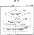
図13は、データ読み出し時の処理フローチャートを表した図である。また、図13の各部ステップの詳細説明のために、図14から図17が使用される。
[Data read processing]
FIG. 13 is a diagram illustrating a processing flowchart when reading data. In addition, FIGS. 14 to 17 are used for detailed description of each step in FIG.
図1において、データ読み出し処理は、命令処理装置4が読み出し対象の論理アドレスを指定することから開始される。 In FIG. 1, the data read process is started when the instruction processing device 4 designates a logical address to be read.
図13のフローでは、ステップS500において、記憶装置2内のメモリコントローラ21が、データバス3およびI/F制御部20を介して、命令処理装置4から読み出し対象の論理アドレスを受信する。
In the flow of FIG. 13, in step S <b> 500, the
次に、メモリコントローラ21は、ステップS51において上記論理アドレスに対応する図6の分割変換テーブル240が、論理/物理アドレス変換テーブルキャッシュ230に存在しているか否かを確認する。存在しない場合には、不揮発性メモリ22から分割変換テーブル240を読み出す処理を行う。ステップS51における読み出し処理の詳細については、図14を用いて後述する。
Next, in step S51, the
ステップS51の処理結果として、指定された論理アドレスに対応する分割変換テーブル240が、論理/物理アドレス変換テーブルキャッシュ230上に入手できた。この場合に、次のステップS501では、論理/物理アドレス変換テーブルキャッシュ230上の分割変換テーブル240を用いて、上記論理アドレスに対応する物理アドレスを特定する。分割変換テーブル240は、図6の構成を備えているので、物理アドレス2203として、物理ブロック番号2204と、物理ページ番号2205の組み合わせが得られている。
As a result of the processing in step S51, the division conversion table 240 corresponding to the designated logical address can be obtained on the logical / physical address
次に、ステップS502では、図11の変換テーブル管理テーブル235において、ステップS501で使用した分割管理テーブル240の追い出しカウント2354を0に変更する。また、上記分割管理テーブル以外の分割管理テーブル240において、キャッシュ有無フラグ2352が1であるテーブルの追い出しカウント2354を1だけ加算する。ステップS502での一連の処理により、論理/物理アドレス変換テーブルキャッシュ230の容量が満杯になった場合に、古い(追い出しカウント2354の数が多い)分割変換テーブル240から順に、不揮発性メモリ22に戻されて書き込まれる。これにより、論理/物理アドレス変換テーブルキャッシュ230の容量が一定に保たれる。
Next, in step S502, the
その後、ステップS503では、ステップS501で特定した物理アドレスを用いて、不揮発性メモリ22からデータ221を読み出す。
Thereafter, in step S503, the
次に、ステップS52では、図1の論理/物理アドレス変換テーブルキャッシュ230の容量が満杯である場合には、不揮発性メモリ22に対して、分割変換テーブル240を書き込む処理を行う。書き込み処理の詳細については、図15を用いて後述する。
Next, in step S52, when the capacity of the logical / physical address
最後に、ステップS504では、命令処理装置4に対して、読み出し終了報告を行う。 Finally, in step S504, a read completion report is sent to the instruction processing device 4.
以上が読み出し時の概略処理であるが、ステップS51およびステップS52は処理をさらに細分化できるので、細分化した処理について説明する。図14は、ステップS51の詳細な処理フローチャートを表した図である。この処理は、論理アドレスに対応する分割変換テーブル240を、読み出すための処理である。 The above is the outline processing at the time of reading, but step S51 and step S52 can be further subdivided, so the subdivided processing will be described. FIG. 14 is a diagram illustrating a detailed processing flowchart of step S51. This process is a process for reading the division conversion table 240 corresponding to the logical address.
ステップS51では、まずステップS510において命令処理装置4から受信した論理アドレスに対応する分割変換テーブル240が、論理/物理アドレス変換テーブルキャッシュ230に保持されているか、図11の変換テーブル管理テーブル235内のキャッシュ有無フラグ2352を用いて確認する。キャッシュ有無フラグ2352が0である場合には、論理/物理アドレス変換テーブルキャッシュ230に保持されていないので、ステップS511の処理に入る。キャッシュ有無フラグ2352が1である場合には、論理/物理アドレス変換テーブルキャッシュ230に保持されているので、ステップS51の処理は終了となる。
In step S51, first, whether or not the division conversion table 240 corresponding to the logical address received from the instruction processing device 4 in step S510 is held in the logical / physical address
ステップS511では、引き続き図11の変換テーブル管理テーブル235の保存フラグ2351が、1である(分割変換テーブル240が不揮発性メモリ22に記憶されている)ことを確認する。保存フラグ2351が1である場合には、ステップS512の処理、0である場合には、ステップS514の処理を実行する。
In step S511, it is confirmed that the
保存フラグ2351が1である場合には、ステップS512において、この分割変換テーブル240の格納先である物理アドレス2356を図11で確認する。
If the
ステップS513では、不揮発性メモリ22から対応する分割変換テーブル240を読み出す。そして、図12のキャッシュ管理テーブル236の有効フラグ2361を確認し、論理/物理アドレス変換テーブルキャッシュ230の空いているエントリに、読み出した分割変換テーブル240の情報を格納する。
In step S513, the corresponding divided conversion table 240 is read from the
なお、ステップS511において保存フラグ2351が0である場合には、ステップS514において図6のキャッシュ管理テーブル236の有効フラグ2361を確認し、論理/物理アドレス変換テーブルキャッシュ230の空いているエントリの選択を行う。
If the
その後、ステップS515において、図11の変換テーブル管理テーブル235のキャッシュ有無フラグ2352を1に変更し、更新フラグ2353と追い出しフラグ2354を0に初期化し、キャッシュエントリ番号2355をステップS513もしくはステップS514で選択したエントリ番号に更新する。また、図12のキャッシュ管理テーブル236において、上記キャッシュエントリ番号2355に対応する有効フラグ2361を1に変更する。以上がステップS51の処理の詳細である。
Thereafter, in step S515, the cache presence /
図15はステップS52の詳細な処理フローチャートを表した図である。ステップS52は、この全体処理により、分割変換テーブル240を不揮発性メモリ22へ書き込む処理を行う。
FIG. 15 is a diagram showing a detailed process flowchart of step S52. In step S52, the division conversion table 240 is written into the
ステップS52の最初のステップS520では、まず論理/物理アドレス変換テーブルキャッシュ230の容量が満杯であるかどうかを確認する。満杯である場合(YES)には、ステップS522側に移り分割変換テーブル240を不揮発性メモリ22へと書き込む処理を行う。満杯でない場合(NO)には、ステップS52の処理は終了となる。
In the first step S520 of step S52, it is first confirmed whether the capacity of the logical / physical address
不揮発性メモリ22への分割変換テーブル240の書き込みを行う場合は、まずステップS521において、図11の変換テーブル管理テーブル235内のキャッシュ有無フラグ2352と追い出しカウント2354を参照する。そして、キャッシュ有無フラグ2352が1(論理/物理アドレス変換テーブルキャッシュ230に保存されている)であり、かつこの中で追い出しカウント2354が最も大きい分割変換テーブル240を書き込み対象として選択する。
When writing the divided conversion table 240 to the
その後、ステップS522において、選択した分割変換テーブル240の更新フラグ2353(図11)を確認し、更新フラグ2353が1(更新あり)である場合には、ステップS53に移り書き込み先ページの特定を行う。更新フラグ2353が0(更新なし)である場合には、ステップS524に移る。なお、ステップS53の詳細は、図16で後述する。
Thereafter, in step S522, the update flag 2353 (FIG. 11) of the selected split conversion table 240 is confirmed. If the
ステップS523では、ステップS53で特定した物理アドレスに対して選択した分割変換テーブル240を書き込む。 In step S523, the division conversion table 240 selected for the physical address specified in step S53 is written.
ステップS54では、書き込み終了後、図7のスクラッチブロック管理テーブル231、図8のデータブロック管理テーブル232、図10の物理ブロック管理テーブル234の更新処理を行う。なお、ステップS54の詳細は、図17で後述する。 In step S54, after the writing is completed, the scratch block management table 231 in FIG. 7, the data block management table 232 in FIG. 8, and the physical block management table 234 in FIG. 10 are updated. Details of step S54 will be described later with reference to FIG.
最後に、ステップS524では、書き込み以前の変換テーブル管理テーブル235(図11)の物理アドレス2356から、図10の物理ブロック管理テーブル234の対応する物理ブロック番号2340を選択し、有効ページ数2342を1つ減算し、有効ページフラグ2343の該当ページ部分を0に更新する。
Finally, in step S524, the corresponding
また、変換テーブル管理テーブル235(図11)において、書き込みを行ったテーブル管理番号2350と対応する保存フラグ2351を1(不揮発性メモリ22に保存)に変更し、キャッシュ有無フラグ2352を0(論理/物理アドレス変換テーブルキャッシュ230に保存せず)に変更する。また、図11の物理アドレス2356の部分を不揮発性メモリ22の書き込み先の物理アドレスに更新する。
Further, in the conversion table management table 235 (FIG. 11), the
そして、書き込みを行った分割管理テーブル240のキャッシュエントリ番号2355(図11)を参照し、図12のキャッシュ管理テーブル236において、対応するキャッシュエントリ番号2360の有効フラグ2361を0(分割管理テーブル240保存せず)に変更する。
Then, referring to the cache entry number 2355 (FIG. 11) of the partition management table 240 that has performed writing, the
なお、ステップS522において、更新フラグ2353が0(更新なし)である場合には、ステップS53、ステップS523、ステップS54の処理は行わない。また、ステップS524でも、物理ブロック管理テーブル234(図10)の更新、変換テーブル管理テーブル235(図11)における物理アドレス2356の更新は行わない。以上がステップS52の処理の詳細である。
Note that if the
図15のステップS52内の主要な処理であるステップS53およびステップS54は、さらに処理を細分化することができる。 Steps S53 and S54 which are main processes in step S52 of FIG. 15 can be further subdivided.
図16は、ステップS53の詳細な処理フローチャートを表した図である。ステップS53の最初のステップS530では、まず書き込み対象の分割変換テーブル240(図6)が所属する論理グループ番号2200に対して、スクラッチブロック2230(図7)が割り当てられているか確認する。この確認は、スクラッチブロック管理テーブル231内で、論理グループ番号2200と一致する論理グループ番号2310のフラグ2312の値を判定することで行う。フラグ2312が1(書き込み可能)であればスクラッチブロック2230が既に割り当てられていると判定し、0(書き込み不可)であれば割り当てられていないと判定する。既に割り当てられている場合には、ステップS533へと移行する。
FIG. 16 is a diagram showing a detailed process flowchart of step S53. In the first step S530 of step S53, first, it is confirmed whether or not the scratch block 2230 (FIG. 7) is assigned to the
割り当てられていない場合には、ステップS531において、図3の消去済みブロック2250の中からブロックを1つ選択して、図7のスクラッチブロック管理テーブル231の物理ブロック番号2313部分に登録し、フラグ2312を1(書き込み可能)に変更する。
If not allocated, in step S531, one block is selected from the erased
その後、ステップS532において、割り当てた図3の消去済みブロック2250に対して、図9の消去済みブロック管理テーブル233内のフラグ2331を0(消去済みブロック群に所属せず)に変更する。
After that, in step S532, the
次に、ステップS533では、図7のスクラッチブロック管理テーブル231を確認し、スクラッチブロック番号2311に対応する物理ブロック番号2313を確認する。
Next, in step S533, the scratch block management table 231 in FIG. 7 is confirmed, and the
そして、ステップS534では、ステップS533で確認した物理ブロック番号2313を、図10の物理ブロック管理テーブル234の物理ブロック番号2340と参照し、該当ブロックの書き込み先ページ番号2344を得る。ステップS53は以上で完了となる。
In step S534, the
また図17は、ステップS54の詳細な処理フローチャートを表した図である。ステップS54の最初のステップS540では、まず書き込みによって図3のスクラッチブロック2230の空きページが無くなったかどうかを確認する。空きページがない場合には、ステップS541の処理に入り、空きページがある場合にはステップS542に移る。
FIG. 17 shows a detailed process flowchart of step S54. In the first step S540 of step S54, it is first confirmed whether or not there is no free page in the
空きページが無くなった場合には、ステップS541において、以下の一連の処理を実行する。まず、図7のスクラッチブロック管理テーブル231において、このスクラッチブロックのフラグ2312を0(書き込み不可)に変更する。その後、図8のデータブロック管理テーブル232において、上記スクラッチブロックが所属していた論理グループ番号2310と対応する論理グループ番号2320の中で、フラグ2322が0(読み出し不可)であるデータブロック番号2321を選択する。そして、選択したデータブロック番号2321のフラグ2322を1(読み出し可能)に変更し、さらに物理ブロック番号2323部分に上記スクラッチブロックの物理ブロック番号2313を登録する。
If there are no more empty pages, the following series of processes is executed in step S541. First, in the scratch block management table 231 of FIG. 7, the
スクラッチブロックに空きページが存在する場合には、ステップS541の処理は行わない。ステップS541もしくはステップS540の後、ステップS542においては、図10の物理ブロック管理テーブル234の有効ページ数2342および書き込み先ページ番号2344を1つ加算し、有効ページフラグ2343を更新する。以上で、ステップS54の処理は終了となる。
If there is an empty page in the scratch block, the process of step S541 is not performed. After step S541 or step S540, in step S542, the
[データ書き込み処理]
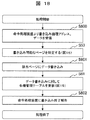
図18は、データ書き込み時の処理フローチャートを表した図である。一部、データ読み出し時と同一のステップS番号を持つ処理が存在するが、これらの処理については処理内容も同一であるため、説明を省略する。
[Data writing process]
FIG. 18 is a diagram illustrating a processing flowchart at the time of data writing. Some processes have the same step S number as that at the time of data reading. However, since the processing contents of these processes are the same, description thereof will be omitted.
データ書き込み処理は、ステップS600において、メモリコントローラ21がデータバス3およびI/F制御部20を介して、命令処理装置4から書き込みデータと論理アドレスを受信するところから開始される。
The data writing process is started when the
次に、メモリコントローラ21は、ステップS53においてデータを書き込む物理アドレスの特定を行う。この処理は図16で詳細に説明したとおりなので、説明は省略する。
Next, the
その後、ステップS601において、ステップS53で特定した物理アドレスに対して、データを書き込む。 Thereafter, in step S601, data is written to the physical address specified in step S53.
ステップS61では、書き込み終了後、各種管理テーブルの更新を行う。この処理は図19を用いて後述する。 In step S61, after completion of writing, various management tables are updated. This process will be described later with reference to FIG.
最後に、ステップS602において、命令処理装置4に対して、書き込み終了報告を行う。 Finally, in step S602, a write completion report is sent to the instruction processing device 4.
以上が書き込み時の処理であるが、ステップS61は処理をさらに細分化できるので、細分化した処理について説明する。図19はステップS61の詳細な処理フローチャートを表した図である。 The above is the processing at the time of writing. Since step S61 can be further subdivided, the subdivided processing will be described. FIG. 19 is a diagram showing a detailed process flowchart of step S61.
ステップS61では、まずステップS54において、データ書き込みに対して、スクラッチブロック管理テーブル231、データブロック管理テーブル232、物理ブロック管理テーブル234の更新処理を行う。この処理は図17で詳細に説明したとおりなので、ここでの説明は省略する。 In step S61, first, in step S54, the scratch block management table 231, the data block management table 232, and the physical block management table 234 are updated for data writing. Since this process has been described in detail with reference to FIG. 17, a description thereof is omitted here.
次に、ステップS51において、分割変換テーブル240の読み出しを行う。この処理は図14で詳細に説明したとおりなので、ここでの説明は省略する。 Next, in step S51, the division conversion table 240 is read. Since this process has been described in detail with reference to FIG. 14, a description thereof is omitted here.
ステップS610では、図3の論理/物理アドレス変換テーブルキャッシュ230上の分割変換テーブル240から、論理アドレスに対応する書き込み前の物理アドレスを特定し、この書き込み前の物理アドレスを用いて物理ロジック管理テーブル234(図10)の有効ページ数2342の減算、及び有効ページフラグ2343の無効化を行う。また、分割変換テーブル240の物理アドレス2203部分を図18のステップS53で特定した物理アドレスに書き換える。
In step S610, the physical address before writing corresponding to the logical address is specified from the divided conversion table 240 on the logical / physical address
その後、ステップS611で、図11の変換テーブル管理テーブル235において、ステップS610で更新した分割変換テーブル240のテーブル管理番号2350に対応する追い出しカウント2354を0に変更する。また、上記以外でキャッシュ有無フラグ2352が1であるテーブル管理番号2350の追い出しフラグ2354を1だけ加算する。
Thereafter, in step S611, the
その後、ステップS52において、分割変換テーブル240の書き込みを行う。この処理は図15で詳細に説明したとおりなので、ここでの説明は省略する。 Thereafter, in step S52, the division conversion table 240 is written. Since this process has been described in detail with reference to FIG. 15, a description thereof is omitted here.
以上がステップS61の処理の詳細である。 The above is the details of the processing in step S61.
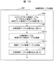
[ブロック消去処理]
図20は、ブロック消去時の処理フローチャートを表した図である。図1のメモリコントローラ21は、ステップS700において、図3の消去済みブロック2250の数が一定数以下になった場合に、ブロック消去処理を開始する。
[Block erase processing]
FIG. 20 is a diagram illustrating a processing flowchart at the time of block erasing. The
まず、ステップS701では、メモリコントローラ21は、図8のデータブロック管理テーブル232を参照し、登録されている物理ブロック番号2323を取得する。取得した物理ブロック番号2323と対応する図10の物理ブロック管理テーブル234内の物理ブロック番号2340の有効ページ数2342を参照する。そして、データブロック管理テーブル232に登録されているブロックの中で、最も有効データページ数の少ないブロックを消去対象として選択する。
First, in step S701, the
次に、ステップS702では、消去対象として選択したブロックの有効ページ数2342が0であるか確認する。
Next, in step S702, it is confirmed whether the number of
有効ページ数2342が0でない場合は、ステップS703において、物理ブロック管理テーブル234の有効ページフラグ2343を参照し、有効ページのデータをスクラッチブロック2230へコピーする。
If the number of
このコピー作業を、選択したブロックの有効ページ数2342が0になるまで繰り返し、有効ページ数2342が0になった場合は、ステップS704に移って、該当ブロックを消去する。
This copying operation is repeated until the number of
最後に、ステップS705では、各種テーブルについての一連の更新処理を実行する。まず、図8のデータブロック管理テーブル232の消去したブロック番号と一致する物理ブロック番号2323のフラグ2322を0(読み出し不可)に変更し、データブロック管理テーブル232からこのブロックの登録を抹消する。そして、消去したブロック番号を図9の消去済みブロック管理テーブル233のフラグ2331が0(消去済みブロック群に所属せず)である消去済みブロック番号2330のエントリに登録し、フラグ2331を1(消去済みブロック群に所属)に変更する。また図10の物理ブロック管理テーブル234において、消去したブロック番号に対応する物理ブロック番号2340の消去回数2341を1つ加算する。
Finally, in step S705, a series of update processing for various tables is executed. First, the
図20の上記消去処理を、消去済みブロック2250の数が一定数以上となるまで繰り返し行う。以上がブロック消去時の処理である。
The above erasure process of FIG. 20 is repeated until the number of erased
なお、本発明は上記の実施例に限定されるものではなく、さまざまな変形例が含まれる。例えば、上記した実施例は本発明を分かりやすく説明するために詳細に説明したものであり、必ずしも説明した全ての構成を備えるものに限定されるものではない。 In addition, this invention is not limited to said Example, Various modifications are included. For example, the above-described embodiments have been described in detail for easy understanding of the present invention, and are not necessarily limited to those having all the configurations described.
また、上記の各構成、機能、処理部、処理手段等は、それらの一部または全部を、例えば集積回路で設計する等によるハードウェアで実現してもよい。また、上記の各構成、機能等は、プロセッサがそれぞれの機能を実現するプログラムを解釈し、実行することによるソフトウェアで実現してもよい。 Each of the above-described configurations, functions, processing units, processing means, and the like may be realized by hardware by designing a part or all of them with, for example, an integrated circuit. In addition, each of the above-described configurations, functions, and the like may be realized by software obtained by the processor interpreting and executing a program that realizes each function.
また、制御線や情報線は説明上必要と考えられるものを示しており、製品上必ずしも全ての制御線や情報線を示しているとは限らない。実際には、殆ど全ての構成が相互に接続されていると考えて良い。 Further, the control lines and information lines indicate what is considered necessary for the explanation, and not all the control lines and information lines on the product are necessarily shown. In practice, it can be considered that almost all the components are connected to each other.
1:計算機
2:記憶装置
3:データバス
4:命令処理装置
5:主記憶メモリ
6:入出力制御装置
7:ネットワーク制御装置
8:表示装置
20:I/F制御部
21:メモリコントローラ
22:不揮発性メモリ
23:RAM
220:論理/物理アドレス変換テーブル
221:データ
230:論理/物理アドレス変換テーブルキャッシュ
231:スクラッチブロック管理テーブル
232:データブロック管理テーブル
233:消去済みブロック管理テーブル
234:物理ブロック管理テーブル
235:変換テーブル管理テーブル
236:キャッシュ管理テーブル
222:ブロック
2220:ページ
2230:スクラッチブロック
2240:データブロック
2250:消去済みブロック
2221:ブロックヘッダページ
2222:データページ
2223:テーブルページ
2224:空きページ
22210:ブロック消去回数
22211:空き領域
22221:データ
22222:ページ属性
22223:論理アドレス
22224:データ書き込み番号
22231:論理/物理アドレス変換テーブル値
22232:ページ属性
22233:テーブル管理番号
22234:テーブル書き込み番号
2200:論理グループ番号
2201:テーブル管理番号
2202:論理アドレス
2203:物理アドレス
240:分割変換テーブル
2310:論理グループ番号
2311:スクラッチブロック番号
2312:フラグ
2313:物理ブロック番号
2320:論理グループ番号
2321:データブロック番号
2322:フラグ
2323:物理ブロック番号
2330:消去済みブロック番号
2331:フラグ
2332:物理ブロック番号
2340:物理ブロック番号
2341:消去回数
2342:有効ページ数
2343:有効ページフラグ
2344:書き込み先ページ番号
2350:テーブル管理番号
2351:保存フラグ
2352:キャッシュ有無フラグ
2353:更新フラグ
2354:追い出しカウント
2355:キャッシュエントリ番号
2356:物理アドレス
2360:キャッシュエントリ番号
2361:有効フラグ
1: Computer 2: Storage device 3: Data bus 4: Instruction processing device 5: Main memory 6: Input / output control device 7: Network control device 8: Display device 20: I / F control unit 21: Memory controller 22: Non-volatile Memory 23: RAM
220: logical / physical address conversion table 221: data 230: logical / physical address conversion table cache 231: scratch block management table 232: data block management table 233: erased block management table 234: physical block management table 235: conversion table management Table 236: Cache management table 222: Block 2220: Page 2230: Scratch block 2240: Data block 2250: Erased block 2221: Block header page 2222: Data page 2223: Table page 2224: Empty page 22210: Block erase count 22211: Empty Area 22221: Data 22222: Page attribute 22223: Logical address 22224: Data write number 22231: Logic Physical address conversion table value 22232: Page attribute 22233: Table management number 22234: Table write number 2200: Logical group number 2201: Table management number 2202: Logical address 2203: Physical address 240: Partition conversion table 2310: Logical group number 2311: Scratch Block number 2312: Flag 2313: Physical block number 2320: Logical group number 2321: Data block number 2322: Flag 2323: Physical block number 2330: Erased block number 2331: Flag 2332: Physical block number 2340: Physical block number 2341: Erase Number of times 2342: Number of valid pages 2343: Valid page flag 2344: Write destination page number 2350: Table management number 2351: Save flag 352: Cache existence flag 2353: update flag 2354: flush Count 2355: cache entry number 2356: Physical Address 2360: cache entry number 2361: valid flag
Claims (9)
前記不揮発性メモリは、命令処理装置が書き込みを行ったデータと、該データの格納場所を管理する論理/物理アドレス変換テーブルを前記ページ単位に分割した複数の分割変換テーブルを有し、
前記RAMは、前記複数の分割変換テーブルのうち少なくとも2つ以上を保存する論理/物理アドレス変換テーブルキャッシュと、前記分割変換テーブルを管理する変換テーブル管理テーブルと、前記論理/物理アドレス変換テーブルキャッシュの管理を行うキャッシュ管理テーブルを有し、
前記変換テーブル管理テーブルは、前記分割変換テーブルが前記論理/物理アドレス変換テーブルキャッシュに保存されていることを示すキャッシュ有無フラグと、前記論理/物理アドレス変換テーブルキャッシュにおける前記分割変換テーブルの保存先を示すキャッシュエントリ番号を有し、
前記キャッシュ管理テーブルは、論理/物理アドレス変換テーブルキャッシュのエントリを前記キャッシュエントリ番号ごとに管理し、各キャッシュエントリ番号に対して保持する有効フラグにより、対応するキャッシュエントリ番号に分割変換テーブルが保存されているか否かを表しており、
前記メモリコントローラは、指定された論理アドレスの分割変換テーブルが論理/物理アドレス変換テーブルキャッシュに保存されていない場合には、不揮発性メモリから該当する分割変換テーブルを読み出すとともに、キャッシュ管理テーブルを参照して空いているエントリに読み出した分割変換テーブルを格納し、
前記不揮発性メモリと前記RAMの間における前記論理/物理アドレス変換テーブルの情報の読み出し及び書き込みは、前記ページ単位で行うことを特徴とする記憶装置。 Nonvolatile memory having a page which is a predetermined writing unit and a block which is a data erasing unit larger than the writing unit, a RAM capable of reading and writing data, and a reading and writing process to the nonvolatile memory and the RAM A storage device having a memory controller for performing
The nonvolatile memory has a plurality of divided conversion tables obtained by dividing the data written by the instruction processing device and the logical / physical address conversion table for managing the storage location of the data into the pages.
The RAM includes a logical / physical address translation table cache that stores at least two or more of the plurality of divided conversion table, the conversion table management table for managing the divided conversion table, the logical / physical address translation table cache Has a cache management table to manage,
The conversion table management table includes a cache presence flag indicating that the divided conversion table is stored in the logical / physical address conversion table cache, and a storage destination of the divided conversion table in the logical / physical address conversion table cache. A cache entry number indicating
The cache management table manages logical / physical address conversion table cache entries for each cache entry number, and the partition conversion table is stored in the corresponding cache entry number by a valid flag held for each cache entry number. Whether or not
The memory controller reads the corresponding partition conversion table from the nonvolatile memory and refers to the cache management table when the partition conversion table of the specified logical address is not stored in the logical / physical address conversion table cache. Store the read conversion table in the free entry,
Reading and writing information of the logical / physical address conversion table between the nonvolatile memory and the RAM is performed in units of pages.
前記論理/物理アドレス変換テーブルキャッシュ内に複数の前記分割変換テーブルを保有している場合に、前記分割変換テーブルのいずれを前記論理/物理アドレス変換テーブルキャッシュから前記不揮発性メモリに書き込むかを、前記分割変換テーブルの使用頻度を示す追い出しカウントによって決定することを特徴とした記憶装置。 The storage device according to claim 1,
If the logical / physical address conversion table cache has a plurality of the divided conversion tables, which of the divided conversion tables is written from the logical / physical address conversion table cache to the nonvolatile memory A storage device characterized by being determined by a eviction count indicating a use frequency of a divided conversion table.
前記論理/物理アドレス変換テーブルキャッシュ内に複数の前記分割変換テーブルを保有し、書き込み対象として選択した前記論理/物理アドレス変換テーブルキャッシュ内の分割変換テーブルを前記論理/物理アドレス変換テーブルキャッシュから前記不揮発性メモリに書き込む場合に、書き込み対象として選択された前記論理/物理アドレス変換テーブルキャッシュ内の前記分割変換テーブルの情報が、前記不揮発性メモリ内の前記分割変換テーブルの情報と一致している場合には、前記書き込み対象として選択された分割変換テーブルの前記不揮発性メモリへの書き込み処理は行わないことを特徴とした記憶装置。 The storage device according to claim 1,
The logical / physical address conversion table cache has a plurality of the divided conversion tables, and the divided conversion table in the logical / physical address conversion table cache selected as a write target is transferred from the logical / physical address conversion table cache to the nonvolatile memory. When writing to the volatile memory, when the information of the partition conversion table in the logical / physical address conversion table cache selected as the write target matches the information of the partition conversion table in the nonvolatile memory The storage device is characterized in that the division conversion table selected as the write target is not written into the nonvolatile memory.
前記不揮発性メモリの記憶領域は、1つ以上のブロックからなるスクラッチブロックと、1つ以上のブロックからなるデータブロックと、1つ以上のブロックからなる消去済みブロックで構成され、
前記RAMは、前記スクラッチブロックの管理を行うスクラッチブロック管理テーブルと、前記データブロックの管理を行うデータ管理テーブルと、前記消去済みブロックの管理を行う消去済みブロック管理テーブルを有し、
前記論理/物理アドレス変換テーブルキャッシュ内の前記分割変換テーブルを前記不揮発性メモリに書き込む場合には、前記スクラッチブロック内の空きページに書き込むとともに、前記変換テーブル管理テーブルを更新し、
前記スクラッチブロックの空きページが無くなった場合には、そのスクラッチブロックを前記データブロックの1つとして扱い、新しいスクラッチブロックとして前記消去済みブロックのうちいずれか1つを割り当て、
前記消去済みブロックが不足した場合には、前記データブロックの中から有効データが少ないブロックを消去対象として選択し、前記消去対象ブロックから有効なデータだけを前記スクラッチブロックにコピーした後、前記消去対象ブロックを消去することを特徴とする記憶装置。 The storage device according to claim 1,
The storage area of the nonvolatile memory is composed of a scratch block composed of one or more blocks, a data block composed of one or more blocks, and an erased block composed of one or more blocks,
The RAM has a scratch block management table for managing the scratch block, a data management table for managing the data block, and an erased block management table for managing the erased block,
When writing the divided conversion table in the logical / physical address conversion table cache to the non-volatile memory, write to an empty page in the scratch block and update the conversion table management table,
If there are no more free pages in the scratch block, treat the scratch block as one of the data blocks, assign any one of the erased blocks as a new scratch block,
When the erased block is insufficient, a block with less valid data is selected as an erasure target from the data blocks, and after copying only valid data from the erasure target block to the scratch block, the erasure target A storage device characterized by erasing a block.
前記RAM内に、各ブロックの消去回数および有効ページ数を管理する物理ブロック管理テーブルを有することを特徴とした記憶装置。 The storage device according to claim 4.
A storage device comprising a physical block management table for managing the number of erases and the number of valid pages of each block in the RAM.
前記スクラッチブロックと前記データブロックを一定量に分割した論理グループ番号ごとに管理することを特徴とする記憶装置。 The storage device according to claim 4.
A storage device that manages each logical group number obtained by dividing the scratch block and the data block into a predetermined amount.
前記記憶装置として、請求項1から請求項6のいずれかに記載の記憶装置を有することを特徴とする計算機。 A computer having an instruction processing device and a storage device,
A computer comprising the storage device according to claim 1 as the storage device.
前記不揮発性メモリは、データの格納場所を管理する論理/物理アドレス変換テーブルを所定の単位に分割した複数の分割変換テーブルを有し、
前記RAMは、前記複数の分割変換テーブルのうち少なくとも2つ以上を保存する論理/物理アドレス変換テーブルキャッシュと、前記分割変換テーブルを管理する変換テーブル管理テーブルと、前記論理/物理アドレス変換テーブルキャッシュの管理を行うキャッシュ管理テーブルを有し、
前記変換テーブル管理テーブルは、前記分割変換テーブルが前記論理/物理アドレス変換テーブルキャッシュに保存されていることを示すキャッシュ有無フラグと、前記論理/物理アドレス変換テーブルキャッシュにおける前記分割変換テーブルの保存先を示すキャッシュエントリ番号を有し、
前記キャッシュ管理テーブルは、論理/物理アドレス変換テーブルキャッシュのエントリを前記キャッシュエントリ番号ごとに管理し、各キャッシュエントリ番号に対して保持する有効フラグにより、対応するキャッシュエントリ番号に分割変換テーブルが保存されているか否かを表しており、
前記メモリコントローラは、指定された論理アドレスの分割変換テーブルが論理/物理アドレス変換テーブルキャッシュに保存されていない場合には、不揮発性メモリから該当する分割変換テーブルを読み出すとともに、キャッシュ管理テーブルを参照して空いているエントリに読み出した分割変換テーブルを格納し、
前記不揮発性メモリと前記RAMの間における前記論理/物理アドレス変換テーブルの情報の読み出し及び書き込みを行うことを特徴とする記憶装置。 A storage device including a nonvolatile memory, a RAM, and a memory controller that performs read and write processing on the nonvolatile memory and the RAM,
The nonvolatile memory has a plurality of divided conversion tables obtained by dividing a logical / physical address conversion table for managing data storage locations into predetermined units,
The RAM includes a logical / physical address translation table cache that stores at least two or more of the plurality of divided conversion table, the conversion table management table for managing the divided conversion table, the logical / physical address translation table cache Has a cache management table to manage,
The conversion table management table includes a cache presence flag indicating that the divided conversion table is stored in the logical / physical address conversion table cache, and a storage destination of the divided conversion table in the logical / physical address conversion table cache. A cache entry number indicating
The cache management table manages logical / physical address conversion table cache entries for each cache entry number, and the partition conversion table is stored in the corresponding cache entry number by a valid flag held for each cache entry number. Whether or not
The memory controller reads the corresponding partition conversion table from the nonvolatile memory and refers to the cache management table when the partition conversion table of the specified logical address is not stored in the logical / physical address conversion table cache. Store the read conversion table in the free entry,
A storage device that reads and writes information of the logical / physical address conversion table between the nonvolatile memory and the RAM.
前記変換テーブル管理テーブルは、前記論理/物理アドレス変換テーブルキャッシュ内に保有する前記分割変換テーブルの中から前記不揮発性メモリに書き込む分割変換テーブルを決定することを特徴とした記憶装置。 The storage device according to claim 8.
The storage device, wherein the conversion table management table determines a divided conversion table to be written in the nonvolatile memory from the divided conversion tables held in the logical / physical address conversion table cache.
Priority Applications (2)
| Application Number | Priority Date | Filing Date | Title |
|---|---|---|---|
| JP2011036717A JP5295286B2 (en) | 2011-02-23 | 2011-02-23 | Storage device and computer equipped with the same |
| US13/372,800 US20120215965A1 (en) | 2011-02-23 | 2012-02-14 | Storage Device and Computer Using the Same |
Applications Claiming Priority (1)
| Application Number | Priority Date | Filing Date | Title |
|---|---|---|---|
| JP2011036717A JP5295286B2 (en) | 2011-02-23 | 2011-02-23 | Storage device and computer equipped with the same |
Publications (3)
| Publication Number | Publication Date |
|---|---|
| JP2012174086A JP2012174086A (en) | 2012-09-10 |
| JP2012174086A5 JP2012174086A5 (en) | 2013-03-14 |
| JP5295286B2 true JP5295286B2 (en) | 2013-09-18 |
Family
ID=46653709
Family Applications (1)
| Application Number | Title | Priority Date | Filing Date |
|---|---|---|---|
| JP2011036717A Expired - Fee Related JP5295286B2 (en) | 2011-02-23 | 2011-02-23 | Storage device and computer equipped with the same |
Country Status (2)
| Country | Link |
|---|---|
| US (1) | US20120215965A1 (en) |
| JP (1) | JP5295286B2 (en) |
Cited By (1)
| Publication number | Priority date | Publication date | Assignee | Title |
|---|---|---|---|---|
| US10156996B2 (en) | 2016-09-06 | 2018-12-18 | Toshiba Memory Corporation | Memory device and read processing method using read counts, first, second, and third addresses |
Families Citing this family (29)
| Publication number | Priority date | Publication date | Assignee | Title |
|---|---|---|---|---|
| US10838646B2 (en) | 2011-07-28 | 2020-11-17 | Netlist, Inc. | Method and apparatus for presearching stored data |
| US10198350B2 (en) | 2011-07-28 | 2019-02-05 | Netlist, Inc. | Memory module having volatile and non-volatile memory subsystems and method of operation |
| US10380022B2 (en) | 2011-07-28 | 2019-08-13 | Netlist, Inc. | Hybrid memory module and system and method of operating the same |
| JP2013097416A (en) | 2011-10-28 | 2013-05-20 | Hitachi Ltd | Storage device and computer |
| US10613982B1 (en) | 2012-01-06 | 2020-04-07 | Seagate Technology Llc | File-aware caching driver |
| US9542324B1 (en) * | 2012-04-05 | 2017-01-10 | Seagate Technology Llc | File associated pinning |
| US9268692B1 (en) | 2012-04-05 | 2016-02-23 | Seagate Technology Llc | User selectable caching |
| JP2013222236A (en) | 2012-04-13 | 2013-10-28 | Hitachi Ltd | Management method of memory, storage device, and computer mounting the same |
| US10282286B2 (en) * | 2012-09-14 | 2019-05-07 | Micron Technology, Inc. | Address mapping using a data unit type that is variable |
| KR20140056657A (en) * | 2012-10-30 | 2014-05-12 | 삼성전자주식회사 | Computer system having main memory and control method thereof |
| US9645942B2 (en) | 2013-03-15 | 2017-05-09 | Intel Corporation | Method for pinning data in large cache in multi-level memory system |
| JP6132010B2 (en) * | 2013-03-19 | 2017-05-24 | 富士通株式会社 | Control device, control program, and control method |
| US9606803B2 (en) | 2013-07-15 | 2017-03-28 | Texas Instruments Incorporated | Highly integrated scalable, flexible DSP megamodule architecture |
| JP5969130B2 (en) * | 2013-07-18 | 2016-08-17 | 株式会社日立製作所 | Information processing device |
| US10248328B2 (en) | 2013-11-07 | 2019-04-02 | Netlist, Inc. | Direct data move between DRAM and storage on a memory module |
| CN111176585A (en) * | 2013-11-07 | 2020-05-19 | 奈特力斯股份有限公司 | Hybrid memory module and system and method for operating the same |
| US11182284B2 (en) | 2013-11-07 | 2021-11-23 | Netlist, Inc. | Memory module having volatile and non-volatile memory subsystems and method of operation |
| US9891825B2 (en) | 2015-01-23 | 2018-02-13 | Toshiba Memory Corporation | Memory system of increasing and decreasing first user capacity that is smaller than a second physical capacity |
| US9715342B2 (en) | 2015-07-03 | 2017-07-25 | Xitore, Inc. | Apparatus, system, and method of logical address translation for non-volatile storage memory |
| US10452556B2 (en) | 2015-09-11 | 2019-10-22 | Toshiba Memory Corporation | Memory device and information processing device |
| TWI584122B (en) * | 2015-11-17 | 2017-05-21 | 群聯電子股份有限公司 | Buffer memory management method, memory control circuit unit and memory storage device |
| CN106776376B (en) * | 2015-11-24 | 2019-08-06 | 群联电子股份有限公司 | Buffer storage supervisory method, memorizer control circuit unit and storage device |
| US10289544B2 (en) * | 2016-07-19 | 2019-05-14 | Western Digital Technologies, Inc. | Mapping tables for storage devices |
| US10126964B2 (en) * | 2017-03-24 | 2018-11-13 | Seagate Technology Llc | Hardware based map acceleration using forward and reverse cache tables |
| JP2019057074A (en) * | 2017-09-20 | 2019-04-11 | 東芝メモリ株式会社 | Memory system |
| CN112988038A (en) * | 2019-12-17 | 2021-06-18 | 国民技术股份有限公司 | Data writing method of nonvolatile memory, terminal and readable storage medium |
| US11947451B2 (en) * | 2020-04-22 | 2024-04-02 | Micron Technology, Inc. | Mapping descriptors for read operations |
| US20220374360A1 (en) * | 2021-05-18 | 2022-11-24 | Macronix International Co., Ltd. | Memory device and method for accessing memory device |
| US20240020223A1 (en) * | 2022-07-18 | 2024-01-18 | Micron Technology, Inc. | Center allocation data structure |
Family Cites Families (14)
| Publication number | Priority date | Publication date | Assignee | Title |
|---|---|---|---|---|
| JP3197815B2 (en) * | 1996-04-15 | 2001-08-13 | インターナショナル・ビジネス・マシーンズ・コーポレ−ション | Semiconductor memory device and control method thereof |
| JP2001142774A (en) * | 1999-11-11 | 2001-05-25 | Toshiba Corp | Memory card and address converting method to be applied to it |
| US6377500B1 (en) * | 1999-11-11 | 2002-04-23 | Kabushiki Kaisha Toshiba | Memory system with a non-volatile memory, having address translating function |
| US8112574B2 (en) * | 2004-02-26 | 2012-02-07 | Super Talent Electronics, Inc. | Swappable sets of partial-mapping tables in a flash-memory system with a command queue for combining flash writes |
| US8051270B2 (en) * | 2005-05-23 | 2011-11-01 | Panasonic Corporation | Memory controller, nonvolatile storage device, nonvolatile storage system, and memory control method |
| US7711923B2 (en) * | 2006-06-23 | 2010-05-04 | Microsoft Corporation | Persistent flash memory mapping table |
| TW200828014A (en) * | 2006-12-28 | 2008-07-01 | Genesys Logic Inc | Flash memory management method with low RAM utilization |
| KR100817087B1 (en) * | 2007-02-13 | 2008-03-27 | 삼성전자주식회사 | Method for operating buffer cache of storage device including flash memory |
| US8656083B2 (en) * | 2007-12-21 | 2014-02-18 | Spansion Llc | Frequency distributed flash memory allocation based on free page tables |
| JP2009282836A (en) * | 2008-05-23 | 2009-12-03 | Panasonic Corp | Memory card and memory card drive |
| JP5221332B2 (en) * | 2008-12-27 | 2013-06-26 | 株式会社東芝 | Memory system |
| US8250333B2 (en) * | 2009-01-05 | 2012-08-21 | Sandisk Technologies Inc. | Mapping address table maintenance in a memory device |
| JPWO2011007511A1 (en) * | 2009-07-16 | 2012-12-20 | パナソニック株式会社 | MEMORY CONTROLLER, NONVOLATILE STORAGE DEVICE, ACCESS DEVICE, NONVOLATILE STORAGE SYSTEM |
| US8688894B2 (en) * | 2009-09-03 | 2014-04-01 | Pioneer Chip Technology Ltd. | Page based management of flash storage |
-
2011
- 2011-02-23 JP JP2011036717A patent/JP5295286B2/en not_active Expired - Fee Related
-
2012
- 2012-02-14 US US13/372,800 patent/US20120215965A1/en not_active Abandoned
Cited By (1)
| Publication number | Priority date | Publication date | Assignee | Title |
|---|---|---|---|---|
| US10156996B2 (en) | 2016-09-06 | 2018-12-18 | Toshiba Memory Corporation | Memory device and read processing method using read counts, first, second, and third addresses |
Also Published As
| Publication number | Publication date |
|---|---|
| US20120215965A1 (en) | 2012-08-23 |
| JP2012174086A (en) | 2012-09-10 |
Similar Documents
| Publication | Publication Date | Title |
|---|---|---|
| JP5295286B2 (en) | Storage device and computer equipped with the same | |
| US20230152969A1 (en) | Memory system and method of controlling memory system | |
| KR101270281B1 (en) | Memory menagement device, information processing device and memory menagement methods | |
| US9026734B2 (en) | Memory system and data deleting method | |
| US9003099B2 (en) | Disc device provided with primary and secondary caches | |
| JP5480913B2 (en) | Storage device and memory controller | |
| US20140129758A1 (en) | Wear leveling in flash memory devices with trim commands | |
| US8909870B2 (en) | Cache evictions from data cache based on content of address translation table cache and address translation table | |
| JP2011128998A (en) | Semiconductor storage device | |
| JP2012203443A (en) | Memory system and control method of memory system | |
| US9122586B2 (en) | Physical-to-logical address map to speed up a recycle operation in a solid state drive | |
| US20190095100A1 (en) | Block Clearing Method | |
| KR101839664B1 (en) | Data storage system and control method thereof | |
| KR101403922B1 (en) | Apparatus and method for data storing according to an access degree | |
| US20100318726A1 (en) | Memory system and memory system managing method | |
| US11150819B2 (en) | Controller for allocating memory blocks, operation method of the controller, and memory system including the controller | |
| JP2012128545A (en) | Memory controller and data recording apparatus | |
| US11687447B1 (en) | Method and apparatus for performing access control of memory device with aid of additional physical address information | |
| JP2023002294A (en) | Memory system and refresh control method | |
| JP2016126737A (en) | Cache memory device and program | |
| JP6430039B2 (en) | Storage device and storage device control method | |
| TWI824761B (en) | Method and apparatus for caching address mapping information in flash memory based storage device | |
| US10747684B2 (en) | Semiconductor device managing address mapping of a semiconductor memory device and data storage device including the semiconductor device | |
| CN114664337A (en) | Method and apparatus for adjusting write window size of flash memory device | |
| TW202336587A (en) | Method and apparatus for caching address mapping information in flash memory based storage device |
Legal Events
| Date | Code | Title | Description |
|---|---|---|---|
| A521 | Request for written amendment filed |
Free format text: JAPANESE INTERMEDIATE CODE: A523 Effective date: 20130125 |
|
| A621 | Written request for application examination |
Free format text: JAPANESE INTERMEDIATE CODE: A621 Effective date: 20130125 |
|
| A131 | Notification of reasons for refusal |
Free format text: JAPANESE INTERMEDIATE CODE: A131 Effective date: 20130319 |
|
| A521 | Request for written amendment filed |
Free format text: JAPANESE INTERMEDIATE CODE: A523 Effective date: 20130510 |
|
| TRDD | Decision of grant or rejection written | ||
| A01 | Written decision to grant a patent or to grant a registration (utility model) |
Free format text: JAPANESE INTERMEDIATE CODE: A01 Effective date: 20130604 |
|
| A61 | First payment of annual fees (during grant procedure) |
Free format text: JAPANESE INTERMEDIATE CODE: A61 Effective date: 20130611 |
|
| R150 | Certificate of patent or registration of utility model |
Ref document number: 5295286 Country of ref document: JP Free format text: JAPANESE INTERMEDIATE CODE: R150 Free format text: JAPANESE INTERMEDIATE CODE: R150 |
|
| LAPS | Cancellation because of no payment of annual fees |