JP5289703B2 - High resolution pattern formation method - Google Patents
High resolution pattern formation method Download PDFInfo
- Publication number
- JP5289703B2 JP5289703B2 JP2006341983A JP2006341983A JP5289703B2 JP 5289703 B2 JP5289703 B2 JP 5289703B2 JP 2006341983 A JP2006341983 A JP 2006341983A JP 2006341983 A JP2006341983 A JP 2006341983A JP 5289703 B2 JP5289703 B2 JP 5289703B2
- Authority
- JP
- Japan
- Prior art keywords
- pattern
- forming
- sacrificial film
- high resolution
- resolution pattern
- Prior art date
- Legal status (The legal status is an assumption and is not a legal conclusion. Google has not performed a legal analysis and makes no representation as to the accuracy of the status listed.)
- Expired - Fee Related
Links
Images


Classifications
-
- H—ELECTRICITY
- H10—SEMICONDUCTOR DEVICES; ELECTRIC SOLID-STATE DEVICES NOT OTHERWISE PROVIDED FOR
- H10K—ORGANIC ELECTRIC SOLID-STATE DEVICES
- H10K71/00—Manufacture or treatment specially adapted for the organic devices covered by this subclass
- H10K71/60—Forming conductive regions or layers, e.g. electrodes
- H10K71/611—Forming conductive regions or layers, e.g. electrodes using printing deposition, e.g. ink jet printing
-
- H—ELECTRICITY
- H05—ELECTRIC TECHNIQUES NOT OTHERWISE PROVIDED FOR
- H05K—PRINTED CIRCUITS; CASINGS OR CONSTRUCTIONAL DETAILS OF ELECTRIC APPARATUS; MANUFACTURE OF ASSEMBLAGES OF ELECTRICAL COMPONENTS
- H05K3/00—Apparatus or processes for manufacturing printed circuits
- H05K3/10—Apparatus or processes for manufacturing printed circuits in which conductive material is applied to the insulating support in such a manner as to form the desired conductive pattern
- H05K3/12—Apparatus or processes for manufacturing printed circuits in which conductive material is applied to the insulating support in such a manner as to form the desired conductive pattern using thick film techniques, e.g. printing techniques to apply the conductive material or similar techniques for applying conductive paste or ink patterns
- H05K3/1241—Apparatus or processes for manufacturing printed circuits in which conductive material is applied to the insulating support in such a manner as to form the desired conductive pattern using thick film techniques, e.g. printing techniques to apply the conductive material or similar techniques for applying conductive paste or ink patterns by ink-jet printing or drawing by dispensing
- H05K3/125—Apparatus or processes for manufacturing printed circuits in which conductive material is applied to the insulating support in such a manner as to form the desired conductive pattern using thick film techniques, e.g. printing techniques to apply the conductive material or similar techniques for applying conductive paste or ink patterns by ink-jet printing or drawing by dispensing by ink-jet printing
-
- H—ELECTRICITY
- H05—ELECTRIC TECHNIQUES NOT OTHERWISE PROVIDED FOR
- H05K—PRINTED CIRCUITS; CASINGS OR CONSTRUCTIONAL DETAILS OF ELECTRIC APPARATUS; MANUFACTURE OF ASSEMBLAGES OF ELECTRICAL COMPONENTS
- H05K2203/00—Indexing scheme relating to apparatus or processes for manufacturing printed circuits covered by H05K3/00
- H05K2203/01—Tools for processing; Objects used during processing
- H05K2203/0104—Tools for processing; Objects used during processing for patterning or coating
- H05K2203/013—Inkjet printing, e.g. for printing insulating material or resist
-
- H—ELECTRICITY
- H10—SEMICONDUCTOR DEVICES; ELECTRIC SOLID-STATE DEVICES NOT OTHERWISE PROVIDED FOR
- H10K—ORGANIC ELECTRIC SOLID-STATE DEVICES
- H10K85/00—Organic materials used in the body or electrodes of devices covered by this subclass
- H10K85/10—Organic polymers or oligomers
- H10K85/111—Organic polymers or oligomers comprising aromatic, heteroaromatic, or aryl chains, e.g. polyaniline, polyphenylene or polyphenylene vinylene
- H10K85/113—Heteroaromatic compounds comprising sulfur or selene, e.g. polythiophene
- H10K85/1135—Polyethylene dioxythiophene [PEDOT]; Derivatives thereof
Landscapes
- Engineering & Computer Science (AREA)
- Manufacturing & Machinery (AREA)
- Microelectronics & Electronic Packaging (AREA)
- Chemical & Material Sciences (AREA)
- Materials Engineering (AREA)
- Application Of Or Painting With Fluid Materials (AREA)
- Exposure And Positioning Against Photoresist Photosensitive Materials (AREA)
- Exposure Of Semiconductors, Excluding Electron Or Ion Beam Exposure (AREA)
- Internal Circuitry In Semiconductor Integrated Circuit Devices (AREA)
Description
本発明は、高解像度パターンの形成方法に関し、特に基板上に付着させた犠牲フィルムからなるパターン鋳型に機能性インクを充填することにより高アスペクト比を有する高解像度パターンを形成する方法に関する。 The present invention relates to a method for forming a high-resolution pattern, and more particularly to a method for forming a high-resolution pattern having a high aspect ratio by filling a functional template into a pattern template made of a sacrificial film attached on a substrate.
電子素子用のパターンを形成するため、一般に光反応による溶解度の差異を利用したフォトリソグラフィが用いられる。具体的には、一定の光に反応するフィルム又は液体からなるフォトレジストに、パターン模様を有するマスクを介して光を選択的に通過させることにより、感光部又は非感光部に選択的に光化学反応を起こさせ、現像、充填、剥離等の工程を経て最終的に所望のパターンを作り出す。 In order to form a pattern for an electronic device, photolithography utilizing a difference in solubility due to a photoreaction is generally used. Specifically, a photochemical reaction selectively occurs in a photosensitive part or a non-photosensitive part by selectively allowing light to pass through a mask having a pattern pattern through a photoresist made of a film or liquid that reacts to a certain amount of light. And a desired pattern is finally produced through processes such as development, filling, and peeling.
しかしながら、フォトリソグラフィには材料の浪費や工程の複雑さ等の問題があった。さらに大面積のマスクを用いるため、新しい設計に短時間で適応するのが難しい。またパターンを形成する機能性材料を積層するのにスパッタリングやCVD等を用いるが、フォトリソグラフィでは短時間でマイクロメートル以上の厚さの機能性材料を積層するのが困難であった。 However, photolithography has problems such as material waste and process complexity. Furthermore, since a large area mask is used, it is difficult to adapt to a new design in a short time. Sputtering, CVD, or the like is used for laminating the functional material for forming a pattern. However, it is difficult to laminate a functional material having a thickness of micrometer or more in a short time by photolithography.
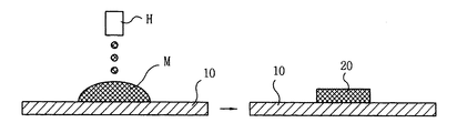
かかる欠点を克服するため、マスクを用いずに直接基板上にパターニングを行うことが可能なインクジェットパターン形成法が提案されている。インクジェットパターン形成法は、図1(a) に示すように、インクジェットプリントヘッドHによりパターンを形成する機能性インクMで基板10上に描画し、乾燥により機能性インクMから液体成分を除去する。
In order to overcome such drawbacks, there has been proposed an ink jet pattern forming method capable of patterning directly on a substrate without using a mask. In the ink jet pattern forming method, as shown in FIG. 1A, the ink is drawn on the
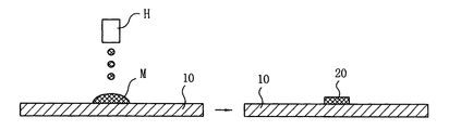
しかしながら、従来のインクジェットを用いたパターン形成法には以下のような問題がある。パターニングすべき機能性材料(比重約10)がインク全体の50体積%を占め、残りが乾燥により除去される液体成分(平均比重約1)と仮定すると、インク全体に対する機能性材料の体積分率は約9%である。さらにインクジェットによりパターニングされた線幅は固定されており、厚さの減少率は均一であると仮定すると、乾燥後のパターン厚は乾燥前より9%程度と極めて薄くなる。図1(a)はこのような現象を概略的に示す。また高解像度パターンを形成するには、すなわちパターン幅を小さくするには、インク滴を小さくするのが一般的であるが、小さいインク滴を使用すると、図1(b) に示すように、単位面積当たりの塗布量が少なくなり、パターンはさらに薄くなる。このように、パターン幅を小さくしつつ所望のパターン厚を得るという2つの目的を同時に達成するのは困難であった。またインク滴を小さくすると、インク滴の弾着誤差がパターンのスケールと比較して相対的に増大し、致命的なパターン誤差になるおそれもある。 However, the conventional pattern forming method using an ink jet has the following problems. Assuming that the functional material to be patterned (specific gravity about 10) occupies 50% by volume of the entire ink and the rest is a liquid component (average specific gravity about 1) that is removed by drying, the volume fraction of the functional material relative to the entire ink Is about 9%. Furthermore, assuming that the line width patterned by ink jet is fixed and the rate of decrease in thickness is uniform, the pattern thickness after drying is as thin as about 9% before drying. FIG. 1 (a) schematically shows such a phenomenon. In order to form a high-resolution pattern, that is, to reduce the pattern width, it is common to make the ink droplets small. However, if small ink droplets are used, the unit as shown in Fig. 1 (b) The coating amount per area is reduced, and the pattern is further thinned. Thus, it has been difficult to simultaneously achieve the two objectives of obtaining a desired pattern thickness while reducing the pattern width. If the ink droplets are made smaller, the impact error of the ink droplets is relatively increased compared to the pattern scale, which may cause a fatal pattern error.
しかも、高解像度のために前記インク滴の大きさを減らす場合、前記インク滴の弾着誤差がパターンのスケールと比較して相対的に増大し、致命的なパターン誤差、すなわち間違ったパターンが形成されるという問題点があった。 In addition, when the size of the ink droplet is reduced for high resolution, the impact error of the ink droplet increases relatively compared to the pattern scale, and a fatal pattern error, that is, an incorrect pattern is formed. There was a problem of being.
従って本発明の目的は、幅に対して十分な厚さを有する高解像度パターンを形成する方法を提供することである。 Accordingly, an object of the present invention is to provide a method of forming a high resolution pattern having a sufficient thickness with respect to the width.
本発明の別の目的は、パターン鋳型を用いて高解像度パターンを形成する際、機能性インクの乾燥によるパターンの厚さの減少を勘案して、パターン鋳型を形成する犠牲フィルムを十分な厚さに選定することにより、輪郭のシャープな高解像度パターンとする方法を提供することである。 Another object of the present invention is to form a sufficient thickness of a sacrificial film for forming a pattern mold in consideration of a decrease in the thickness of the pattern due to drying of the functional ink when forming a high resolution pattern using the pattern mold. It is to provide a method for obtaining a high-resolution pattern having a sharp outline.
上記目的に鑑み鋭意研究の結果、基板上に犠牲フィルムを付着させる工程と、露光及び現像を行って所望のパターン状凹部を有するパターン鋳型を形成する工程と、パターン状凹部に機能性材料を含有するインクを充填する工程と、インクを乾燥させる工程により、所望のパターン厚及び高アスペクト比を有する高解像度パターンが形成されることを発見し、本発明に想到した。 As a result of intensive research in view of the above-mentioned purpose, a step of attaching a sacrificial film on a substrate, a step of performing exposure and development to form a pattern mold having a desired pattern-shaped recess, and a functional material in the pattern-shaped recess The present inventors have found that a high-resolution pattern having a desired pattern thickness and a high aspect ratio can be formed by the step of filling the ink to be dried and the step of drying the ink.
すなわち、本発明の高解像度パターンの形成方法は、基板上に犠牲フィルムを付着させる工程(S1)と、前記犠牲フィルムに集束可能なエネルギービームを用いて露光及び現像を行って所望のパターン状凹部を有するパターン鋳型を形成する工程(S2)と、前記パターン状凹部に機能性材料を含有するインクを充填する工程(S3)と、前記インクを乾燥させる工程(S4)と、前記乾燥工程(S4)後に前記パターン鋳型を除去する工程とを含む高解像度パターンの形成方法であって、
前記犠牲フィルムの厚さを100×β/α以上[ただしαは前記インク中の前記機能性材料の体積分率(体積%)であり、βは前記高解像度パターンの厚さ(μm)である。]とし、
前記基板又は前記パターンを保護する保護層及び前記集束可能なエネルギービームを遮蔽して前記基板を保護する遮光層を積層するか、前記保護層及び前記遮光層の両役割を有する一つの層を設け、
前記機能性材料の除去に必要なエネルギー密度より前記犠牲フィルムの除去に必要なエネルギー密度が低く、前記エネルギービームをパターニングに用いた解像度以上に拡大照射してエネルギー密度を減少させて、前記パターン鋳型のみを除去することを特徴とする。
That is, the method for forming a high resolution pattern of the present invention includes a step (S1) of depositing a sacrificial film on a substrate, and exposure and development using an energy beam that can be focused on the sacrificial film to form a desired pattern-shaped recess. Forming a pattern mold having (S2), filling the pattern-shaped recess with ink containing a functional material (S3), drying the ink (S4), and drying step (S4) And a step of removing the pattern template later,
The thickness of the sacrificial film is 100 × β / α or more [where α is the volume fraction (volume%) of the functional material in the ink, and β is the thickness (μm) of the high resolution pattern. . ]age,
A protective layer that protects the substrate or the pattern and a light-shielding layer that shields the converging energy beam and protects the substrate are stacked, or one layer having both roles of the protective layer and the light-shielding layer is provided. ,
The energy density required to remove the sacrificial film from the energy density required to remove the functional material is rather low, to reduce the energy density to expand irradiating the energy beam or resolution used for patterning the pattern Only the mold is removed.
前記犠牲フィルムの前記基板への付着力を高めるための粘着力又は接着力を有する付着層を設けるのが好ましく、前記基板を保管する際に前記付着層を保護するための除去可能フィルムを設けるのが好ましい。
It is preferable to provide an adhesive layer having an adhesive force or adhesive force for increasing the adhesive force of the sacrificial film to the substrate, and to provide a removable film for protecting the adhesive layer when the substrate is stored . Is preferred.
前記犠牲フィルムは、前記エネルギービームにより容易に除去される物質からなる1層又は複数層からなり、前記基板を保管の際に保護するための最上部の除去可能フィルム、各工程中に発生する汚染を防止するための保護層、前記エネルギービームにより除去が容易な低分子物質、高分子物質又はこれらの組み合わせからなる犠牲フィルム、前記エネルギービームが前記犠牲フィルムの下部へ伝達されるのを遮蔽する遮光層、前記基板と前記犠牲フィルムとの付着を容易にするために前記犠牲フィルムの下面に設けられた、粘着力又は接着力を有する付着層、及び前記付着層へ汚染物質が付着するのを防止するための最下部除去可能フィルムのうち少なくとも1つを設けるのが好ましい。 The sacrificial film is composed of one or more layers made of a material that can be easily removed by the energy beam. The sacrificial film is an uppermost removable film for protecting the substrate during storage, and contamination that occurs during each step. A sacrificial film that is easily removed by the energy beam, a sacrificial film made of a polymer material, or a combination thereof, and a light shield that shields the energy beam from being transmitted to the lower portion of the sacrificial film. Layer, an adhesive layer having an adhesive force or an adhesive force provided on the lower surface of the sacrificial film to facilitate adhesion between the substrate and the sacrificial film, and preventing contaminants from adhering to the adhesive layer It is preferable to provide at least one of the lowermost removable films for the purpose.
最上部の前記除去可能フィルムの下面に、前記犠牲フィルムと前記インクとの濡れ性を調節するために、界面活性剤、ポリマー層又は前記界面活性剤を含むポリマー層がコートされているのが好ましい。 In order to adjust the wettability between the sacrificial film and the ink, the top surface of the removable film is preferably coated with a surfactant, a polymer layer, or a polymer layer containing the surfactant. .
最上部の前記除去可能フィルムを除去した後、前記犠牲フィルムの前記インクとの濡れ性を調節するために界面活性剤をコートするのが好ましい。 After removing the uppermost removable film, it is preferable to coat a surfactant to adjust the wettability of the sacrificial film with the ink.
最上部の前記除去可能フィルムを除去した後、前記犠牲フィルムの前記インクとの濡れ性を調節するために、常圧プラズマ法又はコロナ法のドライ法で表面処理を行うのが好ましい。 After removing the uppermost removable film, it is preferable to perform a surface treatment by a normal pressure plasma method or a corona dry method in order to adjust the wettability of the sacrificial film with the ink.
前記犠牲フィルムは低分子量ポリマーからなり、前記パターン状凹部のコーナー部がシャープであるのが好ましい。 The sacrificial film is preferably made of a low molecular weight polymer, and the corners of the patterned recesses are preferably sharp.
前記犠牲フィルムは高分子量ポリマーからなり、前記パターン状凹部の開口端に盛り上がったリム部が形成されるのが好ましい。 Preferably, the sacrificial film is made of a high molecular weight polymer, and a raised rim is formed at the opening end of the pattern-like recess.
前記犠牲フィルムに前記エネルギービームに対する吸光性を高める吸光剤を添加するのが好ましい。 It is preferable to add a light-absorbing agent that increases the light-absorbing property to the energy beam to the sacrificial film.
前記犠牲フィルムに柔軟剤を添加するのが好ましい。 It is preferable to add a softening agent to the sacrificial film.
前記犠牲フィルムの露光の際、前記エネルギービームとしてレーザ、電子ビーム又は集束イオンビームを用いるのが好ましい。 In the exposure of the sacrificial film, it is preferable to use a laser, an electron beam or a focused ion beam as the energy beam.
前記エネルギービームの出力、径、スキャニング速度及びパターニングに関するデジタルデータを用いて、前記エネルギービームを制御して前記犠牲フィルム上に直接照射するのが好ましい。 Preferably, the energy beam is controlled and directly irradiated onto the sacrificial film using digital data regarding the output, diameter, scanning speed, and patterning of the energy beam.
前記エネルギービームの照射形状を制御するため、マスク又は回折光学素子からなるビームシェーパを用いるのが好ましい。 In order to control the irradiation shape of the energy beam, it is preferable to use a beam shaper composed of a mask or a diffractive optical element.
前記エネルギービームの照射形状を制御するため、マスク又は回折光学素子を用いるのが好ましい。 In order to control the irradiation shape of the energy beam, it is preferable to use a mask or a diffractive optical element.
前記機能性インクの充填工程(S3)後、光硬化等の光化学反応を誘導するのが好ましい。 It is preferable to induce a photochemical reaction such as photocuring after the functional ink filling step (S3).
前記機能性インクの充填工程(S3)後、前記機能性材料に化学的処理を施すのが好ましい。 After the functional ink filling step (S3), the functional material is preferably subjected to chemical treatment.
前記機能性インクの充填工程(S3)後、前記機能性材料を液相から固体相に相変化させるのが好ましい。 After the functional ink filling step (S3), it is preferable to change the phase of the functional material from a liquid phase to a solid phase.
前記機能性インクの充填工程(S3)後、前記機能性材料の特性を向上させるために、前記基板を100℃以上に加熱するのが好ましい。 After the functional ink filling step (S3), the substrate is preferably heated to 100 ° C. or higher in order to improve the characteristics of the functional material.
高解像度パターンにレーザ又はプラズマを照射するのが好ましい。 The high resolution pattern is preferably irradiated with a laser or plasma.
前記犠牲フィルムを溶解させる溶媒又は溶液を用いて前記パターン鋳型及びその上の機能性材料を除去するのが好ましい。 It is preferable to remove the pattern template and the functional material thereon using a solvent or solution that dissolves the sacrificial film.
前記パターン鋳型及びその上の機能性材料を除去する際、前記パターン鋳型の剥離を促進するために加熱を行うのが好ましい。 When removing the pattern mold and the functional material thereon, it is preferable to perform heating in order to promote peeling of the pattern mold.
前記パターン鋳型の除去には、常圧プラズマ、反応性イオンエッチング、紫外線−オゾン法等のドライエッチング法を用いるのが好ましい。 For the removal of the pattern template, it is preferable to use a dry etching method such as atmospheric pressure plasma, reactive ion etching, or ultraviolet-ozone method.
本発明の方法は、厚い犠牲フィルムからなるパターン鋳型を用いるので、機能性材料の浪費を抑えつつ、従来の方法では得難い高アスペクト比を有する高解像度のパターンを効率良く形成することができる。またパターン鋳型のパターン状凹部が、乾燥後の機能性インク(機能性材料)の厚さより深いため、得られる高解像度パターンのエッジはシャープとなる。 Since the method of the present invention uses a pattern mold made of a thick sacrificial film, it is possible to efficiently form a high-resolution pattern having a high aspect ratio that is difficult to obtain with the conventional method while suppressing the waste of the functional material. In addition, since the pattern-shaped concave portion of the pattern mold is deeper than the thickness of the functional ink (functional material) after drying, the edge of the resulting high resolution pattern is sharp.
本発明の高解像度パターンの形成方法を、図2〜図5を参照して以下詳細に説明する。本発明の高解像度パターン形成方法は、基板10上に犠牲フィルム30を付着させる付着工程(S1)と、犠牲フィルム30を所望の形状にパターニングするために、集束可能なエネルギービームを照射してパターン状凹部40を有するパターン鋳型30’を形成する工程(S2)と、パターン状凹部40に機能性インクMを充填する充填工程(S3)と、機能性インクMを乾燥させる工程(S4)とを含む。
A method for forming a high resolution pattern according to the present invention will be described in detail below with reference to FIGS. The high-resolution pattern forming method of the present invention includes a deposition step (S1) for depositing the
特に1μm以上のパターン厚が求められる場合、機能性インクMの乾燥後に残存する機能性材料の体積分率(体積%)をαとし、高解像度パターンの厚さ(μm)をβとすると、100×β/αμm以上の厚さの半固体状又は固体状の犠牲フィルム30を付着させる。犠牲フィルム30を基板10上に付着する方法はラミネータが好ましいが、フィルムを基板10に付着させることが可能な通常の方法も使用できる。
In particular, when a pattern thickness of 1 μm or more is required, when the volume fraction (volume%) of the functional material remaining after drying the functional ink M is α and the thickness (μm) of the high resolution pattern is β, 100 A semi-solid or solid
犠牲フィルム30を集束可能なエネルギービームによりパターニングした後、現像により除去することでパターン鋳型30’を形成する。パターン鋳型30’のパターン状凹部40に充填された機能性インクMに含まれる機能性材料は乾燥後にパターン20として機能する。
After patterning the
機能性材料としては、例えばポリ(3,4-エチレンジオキシチオフェン)-ポリ(4-スチレンスルホネート)等の伝導性有機物、銅又はアルミニウムのナノ粒子等の伝導性無機物、有機金属化合物等の伝導性物質前駆体、電界発光素子に用いられる有/無機蛍光体又は燐光体、電気的絶縁体又は誘電体、及び有/無機半導体物質及びその前駆体よりなる群から選択されたいずれか一つ以上の機能性物質が使用できる。機能性材料はこれらに限定されず、用途によって種々の材料を選択可能である。 Examples of functional materials include conductive organic materials such as poly (3,4-ethylenedioxythiophene) -poly (4-styrenesulfonate), conductive inorganic materials such as copper or aluminum nanoparticles, and conductive materials such as organometallic compounds. Any one or more selected from the group consisting of organic material precursors, organic / inorganic phosphors or phosphors used in electroluminescent devices, electrical insulators or dielectrics, organic / inorganic semiconductor materials and their precursors Can be used. The functional material is not limited to these, and various materials can be selected depending on the application.
前記犠牲フィルム30はエネルギービームにより容易に除去される物質からなるものであれば特に限定されないが、ポジティブ型又はネガティブ型の感光性樹脂からなるのが好ましい。ポジティブ感光性樹脂からなる場合、犠牲フィルム30のパターニングの際に使用したのと同じか異なる集束可能なエネルギービーム、又は犠牲フィルム30の感光に適した波長帯の集束可能なエネルギービームを用いて露光した後、現像により除去するのが好ましい。
The
基板10の材料は上面にパターン20を形成可能な通常用いられるものであれば特に限定されない。
The material of the
パターン20の上面に、必要に応じて、工程中又は前後に発生する汚染物質からパターン20を保護するための保護層、パターン20の下部をエネルギービームの露光から保護するための遮光層、犠牲フィルム30の基板10への付着力を高めるための付着層、付着層を基板10の保管の際に保護するための除去可能フィルムを設けることができる。
If necessary, a protective layer for protecting the
これらの層は単層でも良く、2つ以上の層から選択的に構成しても良い。遮光層と保護層の積層順序は必要に応じて変更可能である。付着層は基板10の最上部に構成するのが好ましく、基板10を保管する際には除去可能フィルムで保護される。除去可能フィルムは、最上部の除去可能フィルムと最下部除去可能フィルムとからなり、最上部の除去可能フィルムは犠牲フィルム30の最上層に位置し、基板10を保管する際に基板10を保護し、最下部除去可能フィルムは犠牲フィルム30の最下層に位置し、付着層へ汚染物質が付着するのを防止する。
These layers may be a single layer or may be selectively configured from two or more layers. The stacking order of the light shielding layer and the protective layer can be changed as necessary. The adhesion layer is preferably constructed on top of the
除去可能フィルムは、容易に除去できるように、例えばパターン20の加工に用いるエネルギービームと同じ又は異なる波長のエネルギービームにより容易に除去可能な物質、その波長を良く吸収する吸光剤を含む物質、又は工程後の洗浄に用いられる溶媒への高い溶解度を有する物質から構成される。なお1つの層で複数の層の役割を担うこともできる。
The removable film is a material that can be easily removed, for example, a material that can be easily removed by an energy beam having the same or different wavelength as the energy beam used to process the
犠牲フィルム30の形成物質は、常温で固体又は半固体状態であり、エネルギービームの照射により気化又は分解される物質であれば特に限定されないが、ポリプロピレンカーボネート等が好ましい。犠牲フィルム30の材料は、用途、溶媒、機能性インクMとの物理/化学的特性、及び使用するエネルギービームを考慮して決定する。
The material for forming the
犠牲フィルム30は、単一又は複数の材料からなる単層又は複数層からなる。複数層からなる場合、基板10と犠牲フィルム30とが容易に付着するように、犠牲フィルム30の下面に、付着力を上昇させるための少なくとも一つの粘着層又は接着層が設けられているのが好ましい。また集束可能なエネルギービームが犠牲フィルム30の下部に伝達されるのを遮蔽するための遮光層、集束可能なエネルギービームにより除去が容易な低分子物質、高分子物質又はこれらの混合物からなる犠牲フィルム、工程中又は工程前に発生する汚染を防止するための、例えばアクリル樹脂からなる保護層、及び除去可能フィルムをさらに設けても良い。
The
犠牲フィルムに低分子ポリマーを用いると、パターン状凹部40のコーナー部分がシャープになる傾向がある。犠牲フィルム30の材料として低分子ポリマーを場合、機能性インクMの犠牲フィルム30及び基板10に対する濡れ性の差異に応じて機能性インクMがパターン状凹部40に自己整列されるか(図4(a) 参照)、又は犠牲フィルム30上とパターン状凹部40内とに互いに剥離して又は弱く連結して充填される(図4(b) 参照)。
When a low molecular weight polymer is used for the sacrificial film, the corner portion of the patterned
犠牲フィルムに高分子ポリマーを用いると、図5(a) 及び図5(b) に示すように、パターン状凹部40の開口端がリム状に盛り上がる。これをリム部41と呼ぶ。機能性インクMの充填の仕方は低分子ポリマーの場合と同じであるが、リム部41が形成されているため、パターン状凹部40内に充填された機能性インクMと、パターン鋳型30’の上面に堆積した機能性インクMとが分断され、パターン鋳型30’上の不要な機能性インクMの除去が容易になる。
When a high molecular weight polymer is used for the sacrificial film, the opening end of the pattern-shaped
除去可能フィルムを除去し、集束エネルギービームを用いてパターン鋳型30’を形成した後、機能性インクMを充填するときの濡れ性を調節するため、表面改質用界面活性剤を最上部の除去可能フィルムの下部にコートするか、犠牲フィルム30又は保護層にあらかじめ含ませるのが好ましい。また界面活性剤を除去可能フィルムの除去後に犠牲フィルム30(パターン鋳型30’)にコートしても良い。表面改質用界面活性剤がコートされてインクとの濡れ性(例えば親水性)が小さい場合、機能性インクMがパターン状凹部40に自己整列される傾向が強くなる。犠牲フィルム30の上面と機能性インクMとの濡れ性が大きい場合、機能性インクMがパターン鋳型30’の上面に薄く広がり、乾燥後、パターン鋳型30’上の機能性インクMとパターン状凹部40内の機能性インクMとが互いに剥離して又は弱く連結して充填される。機能性インクMとの濡れ性(例えば親水性)を有する材料を最上部の除去可能フィルムの下に設けても良い。除去可能フィルムの除去後、常圧プラズマ、コロナ等のドライ処理によって表面性質を所望通りに変更しても良い。
After removing the removable film and forming the
犠牲フィルム30に、基板10との粘着又は接着等の付着性を調節するか、犠牲フィルム30と基板10との間の密着性を増進させるか、機能性インクMとの適切な濡れ性を維持するか、犠牲フィルム30の材質に適切な柔軟性を調節するか、集束エネルギービームの吸収を向上させるために、適切な添加剤を添加しても良い。
Adjust adhesion to the
集束可能なエネルギービームがレーザである場合、犠牲フィルム30の材料をレーザにより誘導された熱を用いて分解/蒸発させるときは可視光線又は赤外線波長レーザが好ましく、犠牲フィルム30の材料を化学反応で除去するときは紫外線波長レーザが好ましい。
When the focusable energy beam is a laser, a visible or infrared wavelength laser is preferred when the
犠牲フィルム30の材料がレーザの波長で最大吸光スペクトルを示す場合は吸光を助けるための添加剤を使用する必要はないが、使用するレーザの波長帯で最大吸光スペクトルを示す添加剤を添加することにより、犠牲フィルム30の除去を容易に行うこともできる。
If the material of the
添加剤としての吸光剤を用いる場合、犠牲フィルム30の材料を溶解する溶液に対して高溶解度を有するが、機能性インクMを溶解する溶液には殆ど溶解されないものが好ましい。熱分解により犠牲フィルム30を除去する場合、比熱及び潜熱が小さいものが好ましい。溶液を用いて選択的に犠牲フィルム30のみを除去する場合、機能性インクMが使用する溶液に溶解しないのが好ましい。
In the case of using a light-absorbing agent as an additive, it is preferable to have a high solubility in a solution that dissolves the material of the
集束可能なエネルギービームとしてレーザを用いる場合、吸収を向上させるために使用される物質として、ジアゾアルキル、ジアゾニウム塩、アジド化合物、アンモニウム塩、オキシド、カーボネート、ペルオキシド及びこれらの混合物を挙げることができるが、赤外線波長のエネルギービームを用いる場合、置換されたポリフタロシアニン化合物、金属含有フタロシアニン化合物、シアニン染料、スクアリリウム染料、カルコゲノピリオアクリリデン染料、クロコニウム染料、金属チオレート染料、ビス(カルコゲノピリオ)ポリメチン染料、オキシインドリジ染料、ビス(アミノアリール)ポリメチン染料、メロシアニン染料、キノイド染料及びこれらの混合物からなる群から選ばれたいずれか一つを使用することができる。また遷移金属元素及びIIIa、IVa、Va、VIa、VIII、IIIb、Vb族に属する元素、又はこれらの混合無機物も使用することができ、炭素のようなIVb族に属する元素も使用することができる。吸光剤は、犠牲フィルム30の材料又は使用するエネルギービームと連関性を有するが、これらに限定されるものではない。柔軟剤としては、ジフェニルフタレート、2−エチルヘキシルフタレート等のフタル酸ジフェニル誘導体、ブチルリシノリエート、プロピレングリコールリシノリエート等のリシノール酸誘導体、ジブチルセバケート、ジメチルセバケート等のセバシン酸誘導体、n−ブチルステアレート、プロピレングリコールモノステアレート等のステアリン酸誘導体、ジエチルサクシネート等のコハク酸誘導体、N−エチル−o,p−トルエン−スルホンアミド等のスルホン酸誘導体、トリクレシルホスフェート、トリブチルホスフェート等のホスホン酸誘導体、クロロパラフィン等のパラフィン誘導体、イソプロピルパルミテート、メチルパルミテート等のパルミチン酸誘導体、ブチルオレエート、グリセロールトリオレエート等のオレイン酸誘導体、イソプロピルミリステート等のミリスチン酸誘導体、トリカプリルトリメリテートやトリイソデシルトリメリテート等のメリト酸、2-n-ブチルマレエート、2−エチルヘキシルマレエート等のマレイン酸誘導体、メチルリノリエート等のリノレン酸誘導体、メチルラウレート等のラウリン酸誘導体、ジペチルイソフタレート、ジメチルイソフタレート等のイソフタル酸誘導体、2,2,4-トリメチル−1,3−ペンタネジオール、ジイソブチレート等のイソ酪酸誘導体、グリセロールトリアセテート等のグリセロール誘導体、ジブチルフタレート等のフマル酸誘導体、n−オクチルエポキシステアレート等のエポキシ誘導体、トリ−n−ブチルシトレート、アセチルトリエチルシトレート等のクエン酸誘導体、ジエチレングリコールジベンゾアート、ジプロピレングリコールジベンゾアート等のベンゾ酸誘導体、ジイソデシルアゼレート、ジメチルアゼレート等のアゼライン酸誘導体、ジカプリルアジペート、ジイソデシルアジペート等のアジピン酸誘導体等を使用することができるが、これらに限定されるものではない。
When using a laser as the focusable energy beam, the materials used to improve absorption can include diazoalkyl, diazonium salts, azide compounds, ammonium salts, oxides, carbonates, peroxides and mixtures thereof. When using an infrared wavelength energy beam, substituted polyphthalocyanine compounds, metal-containing phthalocyanine compounds, cyanine dyes, squarylium dyes, chalcogenopyrioacrylidene dyes, croconium dyes, metal thiolate dyes, bis (chalcogenopyrio) polymethine dyes, oxy Any one selected from the group consisting of indolizy dyes, bis (aminoaryl) polymethine dyes, merocyanine dyes, quinoid dyes and mixtures thereof can be used. Further, transition metal elements and elements belonging to IIIa, IVa, Va, VIa, VIII, IIIb, and Vb groups, or mixed inorganic materials thereof can be used, and elements belonging to IVb group such as carbon can also be used. . The light absorber is related to the material of the
本発明に係るパターン形成方法は、基板10上に犠牲フィルム30を付着させる付着工程(S1)の前後に、集束エネルギービームを用いて除去された犠牲フィルム30の材料が基板10又はパターン20上の他の部位を汚染させないために、保護層を基板10と犠牲フィルム30との間、すなわち基板10の上面又は犠牲フィルム30の下面に設けることができる。保護層は、洗浄工程で極性溶媒が使用される場合には水溶性ポリマー、無極性溶媒が使用される場合には非水溶性ポリマー等が用いられるが、これらに限定されるものではない。保護層及びその除去に用いられる溶液は、機能性インクMに損傷を与えないものが好ましい。
In the pattern forming method according to the present invention, the material of the
本発明のパターン形成方法について以下詳細に説明する。犠牲フィルム30の付着工程(S1)を図2(a)〜2(d) に示す。犠牲フィルム30は基板10にラミネーション等によって付着させるが(図2(a) 参照)、当業界で一般に使用される付着法であれば特に限定されない。作業を容易にするために、必要に応じて加熱しても良い。
The pattern forming method of the present invention will be described in detail below. The attaching process (S1) of the
付着工程(S1)の後、犠牲フィルム30を所望の形状にパターニングするために、集束可能なエネルギービームを照射し、パターン鋳型30’を形成する[工程(S2)](図2(b) 参照)。すなわち、基板10に付着した犠牲フィルム30を所望の形状にパターニングして犠牲フィルム30を部分的に除去し、パターン状凹部40を形成する。レーザ等の集束可能なエネルギービームを用い、エネルギービームの出力、径、スキャニング速度及びパターニングに関するデジタルデータは、コンピュータに入力する。
After the deposition step (S1), in order to pattern the
パターン状凹部40に機能性インクMを充填した後、パターン鋳型30’を除去すると、所望の高解像度パターン20が得られる(図2の(c)及び(d) 参照)。
After the pattern-
パターン鋳型形成工程(S2)で集束可能なエネルギービームの照射の際に、基板10の上面からではなく、下面から照射しても良い。
When irradiating a focusable energy beam in the pattern template forming step (S2), the irradiation may be performed from the lower surface instead of the upper surface of the
エネルギービームを基板10の上面又は下面から照射することにより、犠牲フィルム30を選択的に除去して、パターン鋳型30’を形成する。除去された犠牲フィルム30は、パターン状凹部40又は集束エネルギービームの光学系を汚染するおそれがある。これを防止するために、最上部の除去可能フィルムを除去せずに照射するのが好ましい。
By irradiating the energy beam from the upper surface or the lower surface of the
犠牲フィルム30を選択的に除去してパターン鋳型30’を形成するパターニングに際して、エネルギービームの形状をパターニングに有効に調節するために、回折光学素子やマスクなどのビームシェーパSを部分的に使用することができる。
In patterning for selectively removing the
ビームシェーパSは、従来のフォトリソグラフィにおいて大面積パターニングのためのマスクのみではなく、レーザ等の集束可能なエネルギービームの形状制御のためのビーム経路上に位置した部分的マスクを含む。パターニングされる領域を全てカバーする回折光学素子、又はレーザ等の集束可能なエネルギービームの形状制御のためのビーム経路上に位置した部分的回折光学素子も含む(図3参照)。基板10上には、ビームシェーパS以外のマスク又は回折光学素子の使用なしにエネルギービームを照射する方法、又はビームシェーパSとは別途に基板上にマスク又は回折光学素子を用いてエネルギービームをスキャニングする方法等を用いて、複雑なパターンを形成することができる。ビームシェーパSの他に基板上で使用するマスクは、従来のフォトリソグラフィでのように、大面積パターニングを可能にする大面積マスクのみではなく、基板の一部分にのみ用いられるものも含む。
The beam shaper S includes not only a mask for large area patterning in conventional photolithography but also a partial mask positioned on a beam path for shape control of a focusable energy beam such as a laser. It also includes a diffractive optical element that covers the entire region to be patterned, or a partial diffractive optical element located on the beam path for shape control of a focusable energy beam such as a laser (see FIG. 3). A method of irradiating an energy beam on the
ビームシェーパSは、エネルギービームの形状制御のため、マスクよりは回折光学素子が好ましいが、これに限定されるものではない。 The beam shaper S is preferably a diffractive optical element rather than a mask for controlling the shape of the energy beam, but is not limited thereto.
パターン状凹部40に機能性インクMを充填した後、パターン鋳型30’を除去することにより、高解像度パターン20を形成する[工程(S3)]。
After the functional recess M is filled in the pattern-
機能性インクMの充填方法は通常のものであれば特に限定されず、例えば下記の方法が使用できる。すなわち、機能性インクMを吐出するインクジェット法、ステンシルマスク(スクリーン)及びスキージを用いて基板上にパターンを形成するスクリーン印刷法、正電荷を有する機能性インクを用いる静電気プリント法、機能性材料をブランケットといわれるゴムシートに1回転写し、さらにそのブラケット上の機能性材料を基板に転写する方式のオフセットプリント法、グラビア製板により板を作成した後、オフセット印刷のようにブランケットに機能性材料を一応転写して間接的に基板にプリントするグラビアプリント法、凸板印刷の一種であって、柔軟な樹脂又はゴム凸板を使用するフレキソプリント法、ソフトモールドを用いたプリント法、コートする被コーティング物を回転させながらその中央面に高分子を落下させると、被コーティング物の回転する遠心力により高分子を表面全体にコートするスピンコート法、又はスリットコーターを用いて機能性材料を充填するスリットコーティング法等が使用可能である。 The method of filling the functional ink M is not particularly limited as long as it is a normal one, and for example, the following method can be used. That is, an inkjet method for discharging the functional ink M, a screen printing method for forming a pattern on a substrate using a stencil mask (screen) and a squeegee, an electrostatic printing method using a functional ink having a positive charge, and a functional material. Once the sheet is transferred to a rubber sheet called a blanket and the functional material on the bracket is transferred to the substrate, the board is made by gravure plate, and then the functional material is applied to the blanket as in offset printing. Gravure printing method that temporarily transfers and prints on the substrate indirectly, a kind of convex plate printing, flexographic printing method using flexible resin or rubber convex plate, printing method using soft mold, coating to be coated If a polymer is dropped on the center surface while rotating an object, A spin coating method for coating a polymer on the entire surface by a centrifugal force to rotate the Ingu thereof, or a slit coating method or the like to fill the functional material using a slit coater may be used.
必要な領域にのみインクを吐出するドロップオンデマンド法も使用可能である。ドロップオンデマンド法には、インク吐出の駆動源がヒーター加熱であるサーマル方式と、ピエゾ素子による圧力でインクを押し出す圧電方式とがある。 A drop-on-demand method that ejects ink only in a necessary area can also be used. The drop-on-demand method includes a thermal method in which an ink discharge drive source is heater heating, and a piezoelectric method in which ink is pushed out by pressure by a piezo element.
常にインクを吐出しながら、必要な時間にインクの吐出方向を偏向させて充填する連続インクジェット法も使用可能である。 It is also possible to use a continuous ink jet method in which ink is always ejected and the ink ejection direction is deflected and filled at a required time.
ノズルを介して霧化又は蒸気化した流体ストリームをデジタルデータを用いてパターン状凹部40内に直接充填することもできる。
A fluid stream atomized or vaporized through a nozzle can also be filled directly into the patterned
MAPLE DWやLaser Induced Thermal Imaging (LITI)法等のレーザ転写法によりデジタルデータを用いてパターン状凹部40内に機能性インクMを直接充填することもできる。この際、前記レーザ転写法とは、転写しようとするフィルムを転写紙に製造した後、転写しようとする部分をレーザに露出させてイメージングを行った後、これを基板に移しておき、基板から前記フィルムを取り外すと、帯状にパターニングされる技法をいう。
The functional ink M can also be directly filled into the pattern-
一方、上述したように犠牲フィルム30をレーザなどの集束可能なエネルギービームを用いてパターン鋳型30’を形成した後、インクジェットによりパターン鋳型30’のパターン状凹部40に機能性インクMを充填させて高解像度パターン20を形成する際、充填される機能性インクMと熱、プラズマ、レーザービーム及びイオンビームのいずれか一つとを組み合わせても良い。
On the other hand, after forming the
充填工程(S3)では、ディープコーティング法、すなわち、無電解メッキのためのシード物質をパターン状凹部40に充填させた後、化学反応液に浸漬させて無電解メッキにより高解像度パターン20を形成する方法も用いることができる。また基板10を気相で蒸着する化学気相蒸着方法(CVD法)を用いることもできる。
In the filling step (S3), the seed material for electroless plating is filled in the pattern-shaped
充填工程(S3)中、パターン鋳型30’を有する基板10を加熱することにより充填効率を向上させても良い。
During the filling step (S3), the filling efficiency may be improved by heating the
機能性インクMの充填方法としてインクジェット法が好ましいが、本発明の思想を逸脱しない限り、その他の充填方法も用いることができる。 The ink jet method is preferable as the method for filling the functional ink M, but other filling methods can be used without departing from the concept of the present invention.
機能性インクMの乾燥後に、ブレード、スクレーパ、ワイパー等を用いてパターン鋳型30’ 上に堆積した機能性インクMを除去しても良い。また乾燥後、機能性インクM中の機能性材料(例えば銀ナノインク)の抵抗が高くなる場合がある。この場合、100℃以上で熱処理を施して、機能性材料の粒子を堅く結合させて電気的特性を向上させるのが好ましい。
After the functional ink M is dried, the functional ink M deposited on the
充填工程(S3)後、機能性材料に対して光硬化等の光化学反応を誘導しても良い。すなわち、一般的なUV硬化器により硬化させ、又は電子ビームにより硬化を誘導して、機能性材料の物理/化学的特性を変化させても良い。 After the filling step (S3), a photochemical reaction such as photocuring may be induced on the functional material. That is, curing may be performed by a general UV curing device, or curing may be induced by an electron beam to change the physical / chemical characteristics of the functional material.
充填工程(S3)後、化学的処理による機能性インクMの化学反応を誘導しても良い。具体的には、非電解メッキのためのコロイド状のパラジウムを含んだ溶液をパターン状凹部40に塗布し、パターン鋳型30’を除去した状態又は除去していない状態で、金属イオン,ホルムアルデヒド,ヒドラジン等の還元剤を含む溶液を塗布すると、還元反応により金属パターンを形成することができる。
After the filling step (S3), a chemical reaction of the functional ink M by chemical treatment may be induced. Specifically, a solution containing colloidal palladium for non-electrolytic plating is applied to the pattern-
還元反応以外に、酸化/還元力の差異による置換メッキを用いることもできる。また金属前駆物質をパターン状凹部40に塗布した後、触媒を含む還元液に浸漬させるか又は還元液を選択的に塗布することにより、所望の金属で還元反応を起こすこともできる。
In addition to the reduction reaction, substitution plating based on a difference in oxidation / reduction power can also be used. Further, after applying the metal precursor to the pattern-
本発明の方法は、上記の例に限定されず、本発明の思想を逸脱しない限り、十分な厚さを有する犠牲フィルム30にレーザ等の集束可能なエネルギービームを照射してパターン鋳型30’を形成し、パターン鋳型30’のパターン状凹部40で機能性材料がパターニングされるものを含む。
The method of the present invention is not limited to the above example, and unless it deviates from the idea of the present invention, the
充填工程(S3)後、機能性材料を液相から固相に相変化させても良い。具体的には、液相の金属混合物又は化合物を材料とする機能性材料を含む機能性インクを充填させた後、機能性材料を固相に相変化させても良い。機能性インクMを充填させた後、レーザ又はプラズマを照射して機能性材料の特性を向上させても良い。 After the filling step (S3), the functional material may be changed from a liquid phase to a solid phase. Specifically, the functional material may be changed to a solid phase after being filled with a functional ink containing a functional material made of a liquid phase metal mixture or compound. After the functional ink M is filled, the characteristics of the functional material may be improved by irradiation with laser or plasma.
パターン状凹部40に充填された機能性インクMを乾燥させて液体成分を除去した後[工程(S4)]、パターン鋳型30’を除去することにより、パターン鋳型30’の上面に堆積した不要な機能性インクMも除去され、機能性材料からなる高解像度パターン20のみが残る。
After the functional ink M filled in the pattern-
犠牲フィルム30からなるパターン鋳型30’の除去には、選択的に犠牲フィルムのみを溶解する溶媒又は溶液を使用する方法、熱を加えて犠牲フィルムの剥離を促進する方法、常圧プラズマ、反応性イオンエッチング、UV/O3等のドライエッチング法を用いることができる。
The removal of the
また、パターン鋳型30’及びその上に堆積した機能性インクMの除去は、パターン鋳型30’の形成に用いたエネルギービームをパターン鋳型30’の形成の際の解像度以上に拡大照射することにより行うことができる。すなわち、犠牲フィルム30の材料の除去には50 mJ/cm2以上のエネルギーのレーザが必要であり、機能性材料の除去には200 mJ/cm2以上のエネルギーのレーザが必要であると仮定すると、5μmの直径でエネルギーが200 mJ/cm2のレーザービームを集束させ、犠牲フィルム30の一部を除去して約5μmのパターン鋳型30’を作成する。パターン鋳型30’のパターン状凹部40に機能性インクMを充填して乾燥させた後、残りのパターン鋳型30’(犠牲フィルム30)を除去するために、レーザービームの直径を5μm以上に拡大すると、エネルギー密度が200 mJ/cm2未満に低下するため、機能性材料は除去されないが、パターン鋳型30’を除去することができる。犠牲フィルムの除去することで、その上に積層されている機能性材料も同時に除去できる。すなわち、パターン鋳型30’を形成するためのエネルギービームの解像度以上に拡大照射することにより、パターン鋳型30’の除去に必要なエネルギー密度よりは高いが、機能性材料の除去に必要なエネルギー密度よりは低くなるようにすることにより、パターン鋳型30’のみを除去することができる。
Further, the removal of the
犠牲フィルム30(パターン鋳型30’)は必ずしも除去する必要がない。例えば、パッシベーション又は絶縁等が必要な場合、犠牲フィルム30又はそれを構成する複数の層の少なくとも1層をこれらの用途に適した物質で形成すると、残留したパターン鋳型30’はパッシベーション層又は絶縁層として作用する。パターン鋳型30’の除去後に、熱/化学的処理により高解像度パターン20の特性を向上させても良い。
It is not always necessary to remove the sacrificial film 30 (
本発明の方法によれば、厚い犠牲フィルムからなるパターン鋳型を用いるので、機能性インクの消費を抑えつつ、高アスペクト比を有する高解像度パターンを簡単に形成することができる。 According to the method of the present invention, since a pattern mold made of a thick sacrificial film is used, it is possible to easily form a high resolution pattern having a high aspect ratio while suppressing consumption of functional ink.
10・・・基板
20・・・パターン
30・・・犠牲フィルム
30’・・・パターン鋳型
40・・・パターン状凹部
H・・・インクジェットプリントヘッド
M・・・機能性材料
S・・・ビームシェーパ
10 ... Board
20 ... Pattern
30 ... Sacrificial film
30 '... pattern mold
40 ... Pattern-shaped recess H ... Inkjet print head M ... Functional material
S ... Beam shaper
Claims (15)
前記犠牲フィルムの厚さを100×β/α以上[ただしαは前記インク中の前記機能性材料の体積分率(体積%)であり、βは前記高解像度パターンの厚さ(μm)である。]とし、
前記基板又は前記パターンを保護する保護層及び前記集束可能なエネルギービームを遮蔽して前記基板を保護する遮光層を積層するか、前記保護層及び前記遮光層の両役割を有する一つの層を設け、
前記機能性材料の除去に必要なエネルギー密度より前記犠牲フィルムの除去に必要なエネルギー密度が低く、前記エネルギービームをパターニングに用いた解像度以上に拡大照射してエネルギー密度を減少させて、前記パターン鋳型のみを除去することを特徴とする高解像度パターンの形成方法。
A step (S1) of attaching a sacrificial film on the substrate, a step (S2) of forming a pattern mold having a desired pattern-shaped recess by performing exposure and development using an energy beam that can be focused on the sacrificial film; A step (S3) of filling the pattern-like recess with an ink containing a functional material, a step (S4) of drying the ink, and a step of removing the pattern template after the drying step (S4). A method of forming a resolution pattern,
The thickness of the sacrificial film is 100 × β / α or more [where α is the volume fraction (volume%) of the functional material in the ink, and β is the thickness (μm) of the high resolution pattern. . ]age,
A protective layer that protects the substrate or the pattern and a light-shielding layer that shields the converging energy beam and protects the substrate are stacked, or one layer having both roles of the protective layer and the light-shielding layer is provided. ,
The energy density required to remove the sacrificial film from the energy density required to remove the functional material is rather low, to reduce the energy density to expand irradiating the energy beam or resolution used for patterning the pattern A method for forming a high resolution pattern, wherein only the mold is removed.
Characterized by using a dry etching method of the ozone method - In the method for forming a high resolution pattern according to any one of claims 1 to 14 for the removal of the pattern mold, atmospheric plasma, reactive ion etching, UV A high resolution pattern forming method.
Applications Claiming Priority (2)
| Application Number | Priority Date | Filing Date | Title |
|---|---|---|---|
| KR10-2006-0039985 | 2006-05-03 | ||
| KR1020060039985A KR100690930B1 (en) | 2006-05-03 | 2006-05-03 | Method for preparing a high resolution pattern with a high aspect ratio and the pattern thickness required by using deep ablation |
Publications (3)
| Publication Number | Publication Date |
|---|---|
| JP2007298944A JP2007298944A (en) | 2007-11-15 |
| JP2007298944A5 JP2007298944A5 (en) | 2009-11-05 |
| JP5289703B2 true JP5289703B2 (en) | 2013-09-11 |
Family
ID=38102672
Family Applications (1)
| Application Number | Title | Priority Date | Filing Date |
|---|---|---|---|
| JP2006341983A Expired - Fee Related JP5289703B2 (en) | 2006-05-03 | 2006-12-19 | High resolution pattern formation method |
Country Status (4)
| Country | Link |
|---|---|
| US (1) | US7517467B2 (en) |
| JP (1) | JP5289703B2 (en) |
| KR (1) | KR100690930B1 (en) |
| DE (1) | DE102006058559B4 (en) |
Families Citing this family (22)
| Publication number | Priority date | Publication date | Assignee | Title |
|---|---|---|---|---|
| WO2007084952A2 (en) * | 2006-01-18 | 2007-07-26 | Akrion Technologies, Inc. | Systems and methods for drying a rotating substrate |
| US8053168B2 (en) * | 2006-12-19 | 2011-11-08 | Palo Alto Research Center Incorporated | Printing plate and system using heat-decomposable polymers |
| JP4873160B2 (en) * | 2007-02-08 | 2012-02-08 | トヨタ自動車株式会社 | Joining method |
| DE102007007183A1 (en) * | 2007-02-14 | 2008-08-21 | Man Roland Druckmaschinen Ag | Process for the production of printing plates |
| US20090107546A1 (en) * | 2007-10-29 | 2009-04-30 | Palo Alto Research Center Incorporated | Co-extruded compositions for high aspect ratio structures |
| US8013300B2 (en) * | 2008-06-20 | 2011-09-06 | Carl Zeiss Nts, Llc | Sample decontamination |
| US8200106B2 (en) * | 2009-06-11 | 2012-06-12 | Canon Kabushiki Kaisha | Image forming apparatus with image forming condition control feature based on difference in patch densities |
| KR100969172B1 (en) * | 2009-06-22 | 2010-07-14 | 한국기계연구원 | Method for making fine patterns using mask template |
| MX2012006706A (en) * | 2009-12-16 | 2012-07-03 | Hoffmann La Roche | Detecting the decomposition of enzymes in a test element by means of controlled release of protected analyte. |
| US9472787B2 (en) | 2011-05-23 | 2016-10-18 | Oledworks Gmbh | Fabrication apparatus for fabricating a patterned layer |
| GB2508915A (en) * | 2012-12-14 | 2014-06-18 | Mahle Int Gmbh | A thrust washer for a sliding bearing |
| US10455696B2 (en) | 2013-09-06 | 2019-10-22 | Solvay Specialty Polymers Italy S.P.A. | Electrically conducting assemblies |
| WO2016019223A1 (en) * | 2014-08-01 | 2016-02-04 | Western Michigan University Research Foundation | Self-supported electronic devices |
| CN106660355B (en) | 2014-08-27 | 2019-10-11 | 3M创新有限公司 | The multiple-layer laminated transfer film of electricity |
| KR101654519B1 (en) * | 2015-04-14 | 2016-09-06 | 서울대학교 산학협력단 | Apparatus for manufacturing nano-scale 3-dimensional structure and method thereof |
| CA3001848C (en) * | 2015-10-15 | 2023-09-19 | Board Of Regents, The University Of Texas System | Versatile process for precision nanoscale manufacturing |
| EP3159740B1 (en) * | 2015-10-22 | 2018-08-01 | Flint Group Germany GmbH | Method for generative production of relief printing plates |
| JP6678430B2 (en) * | 2015-11-06 | 2020-04-08 | 株式会社Nbcメッシュテック | Method of forming thin film thin line pattern by screen printing |
| CN105293937A (en) * | 2015-11-29 | 2016-02-03 | 杭州柳茶医药科技有限公司 | Waterproof glass and production technology thereof |
| EP4235750A3 (en) * | 2016-02-15 | 2023-09-06 | Newport Corporation | Method of selectively varying the wetting characteristics of a surface |
| US10746612B2 (en) | 2016-11-30 | 2020-08-18 | The Board Of Trustees Of Western Michigan University | Metal-metal composite ink and methods for forming conductive patterns |
| KR102402471B1 (en) * | 2020-12-22 | 2022-05-26 | 주식회사 셀코스 | Coating method for improved uniformity of surface coating |
Family Cites Families (16)
| Publication number | Priority date | Publication date | Assignee | Title |
|---|---|---|---|---|
| EP0464224B1 (en) | 1990-01-25 | 2000-10-11 | Dai Nippon Insatsu Kabushiki Kaisha | Method of and material for forming thick filmy pattern |
| US6756181B2 (en) * | 1993-06-25 | 2004-06-29 | Polyfibron Technologies, Inc. | Laser imaged printing plates |
| JPH0722732A (en) * | 1993-06-30 | 1995-01-24 | Sumitomo Metal Ind Ltd | Forming method for microwiring |
| US6074893A (en) * | 1993-09-27 | 2000-06-13 | Sumitomo Metal Industries, Ltd. | Process for forming fine thick-film conductor patterns |
| JPH0794848A (en) * | 1993-09-27 | 1995-04-07 | Sumitomo Kinzoku Ceramics:Kk | Formation of conductor layer pattern |
| JP3971489B2 (en) | 1997-08-26 | 2007-09-05 | 太陽インキ製造株式会社 | Glass paste composition and method for manufacturing back plate of plasma display panel using the same |
| JP3686749B2 (en) | 1997-11-04 | 2005-08-24 | 太陽インキ製造株式会社 | Patterned inorganic fired coating film and method for producing plasma display panel |
| WO1999048339A1 (en) * | 1998-03-17 | 1999-09-23 | Seiko Epson Corporation | Substrate for patterning thin film and surface treatment thereof |
| JPH11297213A (en) * | 1998-04-09 | 1999-10-29 | Dainippon Printing Co Ltd | Plasma display panel phosphor screen and its forming method |
| JP2000260309A (en) * | 1999-03-05 | 2000-09-22 | Matsushita Electric Ind Co Ltd | Manufacture of gas discharge panel |
| JP3982231B2 (en) * | 2001-10-19 | 2007-09-26 | セイコーエプソン株式会社 | Color filter manufacturing method, color filter, liquid crystal device, and electronic apparatus |
| JP2005285616A (en) * | 2004-03-30 | 2005-10-13 | Seiko Epson Corp | Thin film forming method, manufacturing method for electro-optical device, manufacturing method for color filter, and liquid droplet discharging device |
| JP2006024695A (en) * | 2004-07-07 | 2006-01-26 | Nec Lcd Technologies Ltd | Wiring forming method using nano particle ink |
| WO2006025016A1 (en) * | 2004-09-03 | 2006-03-09 | Koninklijke Philips Electronics N.V. | Method and apparatus for application of a pattern, element and device provided with such a pattern |
| JP2006073450A (en) * | 2004-09-06 | 2006-03-16 | Idemitsu Kosan Co Ltd | Color transformation substrate, its manufacturing method and organic electroluminescent display device |
| US8796583B2 (en) * | 2004-09-17 | 2014-08-05 | Eastman Kodak Company | Method of forming a structured surface using ablatable radiation sensitive material |
-
2006
- 2006-05-03 KR KR1020060039985A patent/KR100690930B1/en active IP Right Grant
- 2006-12-12 DE DE102006058559A patent/DE102006058559B4/en not_active Expired - Fee Related
- 2006-12-19 JP JP2006341983A patent/JP5289703B2/en not_active Expired - Fee Related
- 2006-12-19 US US11/612,636 patent/US7517467B2/en not_active Expired - Fee Related
Also Published As
| Publication number | Publication date |
|---|---|
| JP2007298944A (en) | 2007-11-15 |
| US7517467B2 (en) | 2009-04-14 |
| KR100690930B1 (en) | 2007-03-09 |
| DE102006058559A1 (en) | 2007-11-15 |
| DE102006058559B4 (en) | 2012-12-06 |
| US20070259474A1 (en) | 2007-11-08 |
Similar Documents
| Publication | Publication Date | Title |
|---|---|---|
| JP5289703B2 (en) | High resolution pattern formation method | |
| JP5356646B2 (en) | High resolution pattern formation method | |
| KR101477998B1 (en) | Compositions and processes for manufacturing printed electronics | |
| JP2007298944A5 (en) | ||
| JP4729730B2 (en) | Inkjet printhead manufacturing method | |
| JP2005319797A (en) | Method for manufacturing nozzle plate for ink jet head, method for manufacturing ink jet head and ink jet head | |
| JP5693068B2 (en) | Liquid discharge head and manufacturing method thereof | |
| US8083324B2 (en) | Inkjet printhead and method of manufacturing the same | |
| JP2006159762A (en) | Patterning method and process for manufacturing ink jet recording head | |
| JP2017121787A (en) | Method of forming partial liquid-repellent region on base material | |
| JP6000715B2 (en) | Method for manufacturing liquid discharge head | |
| CN108944050B (en) | Surface treatment method for nozzle | |
| JP6395503B2 (en) | Ink jet recording head and manufacturing method thereof | |
| US20140307028A1 (en) | Liquid discharge head and method of making the same | |
| JP6921564B2 (en) | Manufacturing method of liquid discharge head | |
| US8945818B2 (en) | Method of manufacturing liquid ejection head | |
| JP5050518B2 (en) | Manufacturing method of resin relief plate, developing device, manufacturing method of printed matter, and manufacturing method of organic EL element | |
| KR20130004343A (en) | Liquid discharge head manufacturing method | |
| JP6061457B2 (en) | Method for manufacturing ink jet recording head | |
| JP2005086188A (en) | Formation method for film pattern and formation equipment, and circuit element | |
| JP5553538B2 (en) | Method for manufacturing liquid discharge head | |
| JP2006035763A (en) | Method for manufacturing inkjet recording head | |
| KR20040069748A (en) | Inkjet printhead and manufacturing method thereof | |
| JP2004306456A (en) | Method for manufacturing liquid jet recording head, liquid jet recording head manufactured thereby, and liquid jet head having treated surface, recorder having the same |
Legal Events
| Date | Code | Title | Description |
|---|---|---|---|
| A521 | Request for written amendment filed |
Free format text: JAPANESE INTERMEDIATE CODE: A523 Effective date: 20090910 |
|
| A621 | Written request for application examination |
Free format text: JAPANESE INTERMEDIATE CODE: A621 Effective date: 20090910 |
|
| A131 | Notification of reasons for refusal |
Free format text: JAPANESE INTERMEDIATE CODE: A131 Effective date: 20111214 |
|
| A601 | Written request for extension of time |
Free format text: JAPANESE INTERMEDIATE CODE: A601 Effective date: 20120313 |
|
| A602 | Written permission of extension of time |
Free format text: JAPANESE INTERMEDIATE CODE: A602 Effective date: 20120316 |
|
| A521 | Request for written amendment filed |
Free format text: JAPANESE INTERMEDIATE CODE: A523 Effective date: 20120413 |
|
| A131 | Notification of reasons for refusal |
Free format text: JAPANESE INTERMEDIATE CODE: A131 Effective date: 20120925 |
|
| A521 | Request for written amendment filed |
Free format text: JAPANESE INTERMEDIATE CODE: A523 Effective date: 20121225 |
|
| A131 | Notification of reasons for refusal |
Free format text: JAPANESE INTERMEDIATE CODE: A131 Effective date: 20130122 |
|
| A521 | Request for written amendment filed |
Free format text: JAPANESE INTERMEDIATE CODE: A523 Effective date: 20130422 |
|
| A01 | Written decision to grant a patent or to grant a registration (utility model) |
Free format text: JAPANESE INTERMEDIATE CODE: A01 Effective date: 20130514 |
|
| A61 | First payment of annual fees (during grant procedure) |
Free format text: JAPANESE INTERMEDIATE CODE: A61 Effective date: 20130605 |
|
| R250 | Receipt of annual fees |
Free format text: JAPANESE INTERMEDIATE CODE: R250 |
|
| LAPS | Cancellation because of no payment of annual fees |