JP5286455B1 - Mask blank, transfer mask, and manufacturing method thereof - Google Patents
Mask blank, transfer mask, and manufacturing method thereof Download PDFInfo
- Publication number
- JP5286455B1 JP5286455B1 JP2013015458A JP2013015458A JP5286455B1 JP 5286455 B1 JP5286455 B1 JP 5286455B1 JP 2013015458 A JP2013015458 A JP 2013015458A JP 2013015458 A JP2013015458 A JP 2013015458A JP 5286455 B1 JP5286455 B1 JP 5286455B1
- Authority
- JP
- Japan
- Prior art keywords
- thin film
- mask blank
- film
- thickness
- main surface
- Prior art date
- Legal status (The legal status is an assumption and is not a legal conclusion. Google has not performed a legal analysis and makes no representation as to the accuracy of the status listed.)
- Active
Links
Images


Classifications
-
- G—PHYSICS
- G03—PHOTOGRAPHY; CINEMATOGRAPHY; ANALOGOUS TECHNIQUES USING WAVES OTHER THAN OPTICAL WAVES; ELECTROGRAPHY; HOLOGRAPHY
- G03F—PHOTOMECHANICAL PRODUCTION OF TEXTURED OR PATTERNED SURFACES, e.g. FOR PRINTING, FOR PROCESSING OF SEMICONDUCTOR DEVICES; MATERIALS THEREFOR; ORIGINALS THEREFOR; APPARATUS SPECIALLY ADAPTED THEREFOR
- G03F1/00—Originals for photomechanical production of textured or patterned surfaces, e.g., masks, photo-masks, reticles; Mask blanks or pellicles therefor; Containers specially adapted therefor; Preparation thereof
- G03F1/26—Phase shift masks [PSM]; PSM blanks; Preparation thereof
- G03F1/32—Attenuating PSM [att-PSM], e.g. halftone PSM or PSM having semi-transparent phase shift portion; Preparation thereof
-
- G—PHYSICS
- G03—PHOTOGRAPHY; CINEMATOGRAPHY; ANALOGOUS TECHNIQUES USING WAVES OTHER THAN OPTICAL WAVES; ELECTROGRAPHY; HOLOGRAPHY
- G03F—PHOTOMECHANICAL PRODUCTION OF TEXTURED OR PATTERNED SURFACES, e.g. FOR PRINTING, FOR PROCESSING OF SEMICONDUCTOR DEVICES; MATERIALS THEREFOR; ORIGINALS THEREFOR; APPARATUS SPECIALLY ADAPTED THEREFOR
- G03F1/00—Originals for photomechanical production of textured or patterned surfaces, e.g., masks, photo-masks, reticles; Mask blanks or pellicles therefor; Containers specially adapted therefor; Preparation thereof
- G03F1/26—Phase shift masks [PSM]; PSM blanks; Preparation thereof
-
- G—PHYSICS
- G03—PHOTOGRAPHY; CINEMATOGRAPHY; ANALOGOUS TECHNIQUES USING WAVES OTHER THAN OPTICAL WAVES; ELECTROGRAPHY; HOLOGRAPHY
- G03F—PHOTOMECHANICAL PRODUCTION OF TEXTURED OR PATTERNED SURFACES, e.g. FOR PRINTING, FOR PROCESSING OF SEMICONDUCTOR DEVICES; MATERIALS THEREFOR; ORIGINALS THEREFOR; APPARATUS SPECIALLY ADAPTED THEREFOR
- G03F1/00—Originals for photomechanical production of textured or patterned surfaces, e.g., masks, photo-masks, reticles; Mask blanks or pellicles therefor; Containers specially adapted therefor; Preparation thereof
- G03F1/38—Masks having auxiliary features, e.g. special coatings or marks for alignment or testing; Preparation thereof
-
- G—PHYSICS
- G03—PHOTOGRAPHY; CINEMATOGRAPHY; ANALOGOUS TECHNIQUES USING WAVES OTHER THAN OPTICAL WAVES; ELECTROGRAPHY; HOLOGRAPHY
- G03F—PHOTOMECHANICAL PRODUCTION OF TEXTURED OR PATTERNED SURFACES, e.g. FOR PRINTING, FOR PROCESSING OF SEMICONDUCTOR DEVICES; MATERIALS THEREFOR; ORIGINALS THEREFOR; APPARATUS SPECIALLY ADAPTED THEREFOR
- G03F1/00—Originals for photomechanical production of textured or patterned surfaces, e.g., masks, photo-masks, reticles; Mask blanks or pellicles therefor; Containers specially adapted therefor; Preparation thereof
- G03F1/54—Absorbers, e.g. of opaque materials
Abstract
【課題】加熱処理および強制冷却処理後に透過率の面内均一性が所定の許容範囲内になるマスクブランク及びその製造方法等を提供する。
【解決手段】本発明のマスクブランクは、透光性基板の主表面上に、転写パターン形成用の薄膜を備えたマスクブランクであって、前記薄膜は、遷移金属とケイ素を含有し、さらに酸素または窒素のうち少なくともいずれかを含有する材料からなり、前記薄膜は、その表層に前記表層を除く領域の薄膜よりも酸素含有量が多い酸化層を有し、前記薄膜は、主表面側における外周部の厚さよりも中央部の厚さが厚く形成されており、前記酸化層は、主表面側における外周部の厚さよりも中央部の厚さが厚く形成されていることを特徴としている。
【選択図】図1The present invention provides a mask blank in which the in-plane uniformity of transmittance is within a predetermined allowable range after a heat treatment and a forced cooling treatment, a manufacturing method thereof, and the like.
A mask blank of the present invention is a mask blank having a transfer pattern forming thin film on a main surface of a translucent substrate, the thin film containing a transition metal and silicon, and further containing oxygen. Or made of a material containing at least one of nitrogen, and the thin film has an oxide layer having a higher oxygen content than a thin film in a region excluding the surface layer on the surface layer, and the thin film has an outer periphery on the main surface side The thickness of the central portion is larger than the thickness of the central portion, and the oxide layer is characterized in that the thickness of the central portion is thicker than the thickness of the outer peripheral portion on the main surface side.
[Selection] Figure 1
Description
本発明は、マスクブランク、転写用マスクおよびこれらの製造方法等に関する。 The present invention relates to a mask blank, a transfer mask, a manufacturing method thereof, and the like.
従来、MoSiNやMoSiON等からなるハーフトーン位相シフト膜(以下、位相シフト膜という。)を備えたマスクブランクは広く知られている。このマスクブランクの製造においては、枚葉式スパッタ装置によって、透光性基板の主表面に位相シフト膜を成膜するのが一般的である。通常の枚葉式スパッタ装置は、成膜室内の下方に透光性基板を載置する回転ステージが設けられており、回転ステージの直上にターゲットが配置されている。しかし、ハーフトーン位相シフト膜の成膜に通常の枚葉式スパッタ装置を用いた場合、透光性基板の主表面形状が矩形であることに起因し、主表面の外周側の膜厚が中心側の膜厚よりも相対的に薄くなりやすいという問題があった。位相シフト膜は、露光光を所定の透過率で透過する機能と、透過する露光光に対して、その位相シフト膜の膜厚と同じ距離だけ空気中を通過する露光光との間で所定の位相差を生じさせる機能が同時に求められる。成膜された位相シフト膜の面内での膜厚分布に偏りがあると、面内での透過率分布のばらつきが生じたり、面内での位相差分布にばらつきが生じたりする恐れがある。また、MoSiNやMoSiONのように、ターゲット材にケイ素を含有する材料が使用され、透光性基板上に酸素や窒素を含有する材料の位相シフト膜をDCスパッタ法で成膜する場合、ケイ素の窒化物やケイ素の酸化物は導電性が低いことから、ターゲット表面でチャージアップによるパーティクルが発生しやすい。このパーティクルは、ターゲット表面の直下にある透光性基板上に落下し、位相シフト膜に入ることで欠陥になってしまう恐れがある。つまり、欠陥発生率が上昇してしまうという問題もある。 Conventionally, a mask blank provided with a halftone phase shift film (hereinafter referred to as a phase shift film) made of MoSiN, MoSiON or the like is widely known. In the production of this mask blank, it is common to form a phase shift film on the main surface of the translucent substrate using a single wafer sputtering apparatus. In a normal single wafer sputtering apparatus, a rotary stage on which a light-transmitting substrate is placed is provided below a film forming chamber, and a target is arranged immediately above the rotary stage. However, when an ordinary single-wafer sputtering apparatus is used for forming the halftone phase shift film, the film thickness on the outer peripheral side of the main surface is the center because the main surface shape of the translucent substrate is rectangular. There has been a problem that the film tends to be relatively thinner than the film thickness on the side. The phase shift film has a predetermined function between the function of transmitting the exposure light with a predetermined transmittance and the exposure light passing through the air by the same distance as the film thickness of the phase shift film with respect to the transmitted exposure light. A function for causing a phase difference is required at the same time. If the thickness distribution in the plane of the formed phase shift film is uneven, there may be a variation in the transmittance distribution within the plane or a variation in the phase difference distribution within the plane. . Further, a material containing silicon is used as a target material, such as MoSiN or MoSiON, and when a phase shift film of a material containing oxygen or nitrogen is formed on a light-transmitting substrate by a DC sputtering method, Since nitride and silicon oxides have low conductivity, particles due to charge-up are likely to occur on the target surface. The particles may fall on the light-transmitting substrate directly below the target surface and enter the phase shift film to cause defects. That is, there is a problem that the defect occurrence rate is increased.
このような矩形状のマスクブランクをスパッタ法で成膜する場合に生じる特有の問題を解決するため、特開2002−090978号公報(特許文献1)に開示されているような、枚葉式スパッタ装置が使用されている。このスパッタ装置は、透光性基板を載置する回転ステージに対して、ターゲットを斜め上方に配置し、透光性基板とターゲットとの間で水平距離と垂直距離の両方を取っている(図2参照)。このような構成のスパッタ装置(いわゆる斜入射スパッタ方式のスパッタ装置)を用いて透光性基板上に位相シフト膜を成膜することで、基板の中心側の膜厚が相対的に厚くなることを抑制でき、かつターゲット表面でのチャージアップに起因する欠陥を低減することができていた。 In order to solve a peculiar problem that occurs when such a rectangular mask blank is formed by sputtering, single-wafer sputtering as disclosed in JP-A-2002-090978 (Patent Document 1). The device is in use. In this sputtering apparatus, a target is disposed obliquely above a rotary stage on which a translucent substrate is placed, and both a horizontal distance and a vertical distance are taken between the translucent substrate and the target (see FIG. 2). By forming a phase shift film on a translucent substrate using a sputtering apparatus having such a configuration (so-called oblique incidence sputtering system sputtering apparatus), the film thickness on the center side of the substrate becomes relatively thick. And defects due to charge-up on the target surface could be reduced.
一方、MoSiNやMoSiONのような金属とケイ素を含有する材料からなる薄膜は、この薄膜を有するマスクブランクから転写用マスクを作製したときに、その転写用マスクはマスクに照射される露光光に対する耐光性があまり高くないという問題があった。また、マスクブランクから転写用マスクを作製するプロセスで使用される薬液や、出来上がった転写用マスクに対して行われる洗浄の際に用いられる洗浄液に対する耐性もあまり高くない。さらに、この材料の薄膜は、比較的大きな圧縮応力を有する傾向もある。これらの問題を解決するために、例えば、特開2002−162726号公報(特許文献2)に開示されているように、金属とケイ素と窒素を含有する光半透過膜を成膜したガラス基板に対し、加熱処理を行っている。 On the other hand, a thin film made of a metal and silicon-containing material such as MoSiN or MoSiON is light-resistant to exposure light irradiated to the mask when the transfer mask is produced from a mask blank having this thin film. There was a problem that the nature was not so high. In addition, the resistance to chemicals used in a process for producing a transfer mask from a mask blank and a cleaning liquid used in cleaning performed on the completed transfer mask is not so high. Furthermore, thin films of this material also tend to have a relatively large compressive stress. In order to solve these problems, for example, as disclosed in Japanese Patent Application Laid-Open No. 2002-162726 (Patent Document 2), a glass substrate on which a light semi-transmissive film containing metal, silicon, and nitrogen is formed is used. On the other hand, heat treatment is performed.
一方、金属とケイ素と窒素を含有する光半透過膜を備えるマスクブランクに対して、空気中または酸素を含有する気体中で加熱処理を行うことで、耐光性を向上させることができる。このマスクブランクに対して加熱処理を行う場合、加熱処理後のマスクブランクを自然冷却すると、光半透過膜の光学特性の面内ばらつきが大きくなるという問題があった。この問題を解決するために、例えば、特開2006−323236号公報(特許文献3)に開示されているように、加熱処理を行った直後のマスクブランクに対して、冷却手段を用いて強制的に冷却する処理を行っている。 On the other hand, light resistance can be improved by performing a heat treatment on a mask blank including a light semi-transmissive film containing metal, silicon, and nitrogen in air or in a gas containing oxygen. When heat-treating the mask blank, there is a problem that in-plane variation of the optical characteristics of the light semi-transmissive film becomes large when the heat-treated mask blank is naturally cooled. In order to solve this problem, for example, as disclosed in Japanese Patent Application Laid-Open No. 2006-323236 (Patent Document 3), the mask blank immediately after the heat treatment is forcibly used using a cooling unit. The cooling process is performed.
遷移金属とケイ素と窒素とを含有する材料からなる薄膜(光半透過膜等)は、空気中または酸素を含有する気体中で加熱処理を行うと、薄膜の表面から酸素を取り込み、膜中の他の領域よりも酸素濃度が高い層(酸化層)が形成される。この薄膜に対して、加熱処理を行う場合、そしてさらに強制冷却処理も行う場合、1枚のマスクブランクに対してそれぞれ処理を行う、いわゆる枚葉式処理の方が、薄膜の酸化層の面内における膜厚分布の均一性を高くすることができ、その結果、処理後の薄膜における光学特性の面内ばらつきをより小さくすることができる。しかし、スループットを考慮すると、複数枚のマスクブランクを一度に処理する、いわゆるバッチ式処理の方が望ましい。複数枚のマスクブランクに対し、バッチ式で加熱処理を行う場合、加熱装置としては、例えば、特許文献2の図5に開示されているような縦型炉が用いられる。 A thin film (such as a light semi-transmissive film) made of a material containing a transition metal, silicon, and nitrogen takes oxygen from the surface of the thin film when heated in air or in a gas containing oxygen. A layer (oxide layer) having a higher oxygen concentration than other regions is formed. When heat treatment is performed on this thin film, and when forced cooling is also performed, so-called single wafer processing is performed in the plane of the thin film oxide layer. As a result, the in-plane variation of the optical characteristics of the thin film after processing can be further reduced. However, in consideration of the throughput, so-called batch processing, in which a plurality of mask blanks are processed at a time, is preferable. In the case of performing heat treatment on a plurality of mask blanks in a batch manner, for example, a vertical furnace as disclosed in FIG.
この縦型炉は、石英チューブの内部に、石英ボードが設けられている。この石英ボードに複数のマスクブランクを載置することによって、石英チューブの内部において、複数のマスクブランクは互いに所定の間隔をおいて縦積みに配置される。このようなマスクブランクの配置状態で、石英チューブの外周に配置されたヒーターによって、加熱処理が行われる。このとき、マスクブランクに対して、ヒーターは端面側(外周側)の位置にあるため、ヒーターからの熱はマスクブランクの外周側から加わる。また、加熱処理終了後、自然冷却でマスクブランクを冷却する場合、石英チューブからの余熱がマスクブランクの外周側に多く付与されるため、冷めにくくなる。また、自然冷却の場合、薄膜の表面温度がゆっくり低下しながら薄膜の表面から酸素が取り込まれていく。このため、薄膜の表面における酸素の取り込み量が面内で大きくばらつき、薄膜の酸化層の面内における膜厚分布のばらつきが生じやすくなる。これらのことから、複数のマスクブランクに対し、縦型炉を用いて加熱処理し、その後、自然冷却する方法を適用した場合、薄膜の光学特性のばらつきを抑制することが困難であった。 In this vertical furnace, a quartz board is provided inside a quartz tube. By placing a plurality of mask blanks on this quartz board, the plurality of mask blanks are arranged vertically at predetermined intervals inside the quartz tube. In such a mask blank arrangement state, heat treatment is performed by a heater arranged on the outer periphery of the quartz tube. At this time, since the heater is located on the end face side (outer peripheral side) with respect to the mask blank, heat from the heater is applied from the outer peripheral side of the mask blank. In addition, when the mask blank is cooled by natural cooling after the heat treatment is completed, a large amount of residual heat from the quartz tube is applied to the outer peripheral side of the mask blank, which makes it difficult to cool. In the case of natural cooling, oxygen is taken in from the surface of the thin film while the surface temperature of the thin film is slowly lowered. For this reason, the amount of oxygen uptake on the surface of the thin film varies greatly in the plane, and the film thickness distribution in the plane of the oxide layer of the thin film tends to vary. For these reasons, when a method of heat-treating a plurality of mask blanks using a vertical furnace and then naturally cooling is applied, it is difficult to suppress variations in optical characteristics of the thin film.
このため、本発明者は、マスクブランクの加熱処理に縦型炉を用いる場合において、加熱処理に引き続いて強制冷却処理を行えるような縦型炉を鋭意検討した。その結果、図3に示すような縦型炉100の構成を見出した。図3の縦型炉100は、特許文献2に開示されている縦型炉とは、2層構造の石英チューブ10における外管10Aの内壁と内管10Bの外壁に挟まれる空間に冷媒を導入することで、内管10Bを強制的に冷却できる機能(冷却器)を有する点が大きく異なる。この機能によって、内管10Bの内部空間である加熱冷却室17内(炉内)の気体やマスクブランク3,5を強制的に冷却することができる。外管の上部と下部には、冷媒を空間内に流入および流出させるための冷媒管11,12を備えている。マスクブランクに対して加熱処理する際に晒す気体(空気、酸素を含有する気体等)を加熱冷却室17内に流入および流出させるための、気体流入管13および気体流出管14を備えている。外管10Aの外周には、マスクブランクを加熱処理する際に使用するヒーター(加熱器)15が設けられている。そして、炉内には、複数のマスクブランク3,5を載置するための石英ボード16が設置されている。
For this reason, when this inventor used a vertical furnace for the heat processing of a mask blank, the present inventor earnestly examined the vertical furnace which can perform forced cooling processing following heat processing. As a result, the configuration of the
このような縦型炉100を使用することによって、複数のマスクブランクをバッチ式で、加熱処理および強制冷却処理を行うことが実現できる。しかし、このようなバッチ式の加熱処理および強制冷却処理を行った場合であっても、処理後のマスクブランクにおける薄膜の光学特性の面内ばらつきを抑制することが難しいことが判明した。この縦型炉100は、強制冷却処理を行う際、冷媒によって、石英チューブ10の内管10Bが冷やされ、さらに内管10Bの内壁を介して加熱冷却室17の気体が冷却されるようになっている。複数のマスクブランクは、水平方向に配置されているため、最初にマスクブランク(薄膜)の端面側(外周側)が強制冷却される。そして、薄膜は端面側から中央側に向かって順に強制冷却されていく。薄膜は表面温度が所定以上の状態では酸素を多く取り込むが、薄膜の表面温度が急速に低下すると酸素を取り込む量が大幅に低下する。
By using such a
図4に、縦型炉100を用いて、加熱処理および強制冷却処理を行った後のマスクブランク5の断面を示す。このマスクブランク5は、透光性基板1上に、遷移金属とケイ素と窒素を含有する材料からなる薄膜4を形成する工程において、図2に示すような斜入射スパッタ方式のスパッタ装置を用い、主表面内における膜厚均一性が高い薄膜となるような条件で薄膜4を形成したものである。すなわち、薄膜4の中央部(中央側の領域)の膜厚Hc4と外周部(外周側の領域)の膜厚Ho4はほぼ同じとなっている。このマスクブランク5は、前記のとおり、薄膜4の成膜後、縦型炉100で加熱処理および強制冷却処理を行っている。それらの処理後のマスクブランク5は、薄膜4の外周部では酸化層42の厚さが相対的に薄くなり、薄膜の中央部では、酸化層42の厚さが相対的に厚くなっている(酸化層42を除く薄膜4の領域41は、外周部で厚さが相対的に厚く、中央部で厚さが相対的に薄くなっている。)。すなわち、中央部の酸化層42の膜厚Hc42が外周部の酸化層42の膜厚Ho42よりも厚い(酸化層42を除く薄膜4の領域41は、中央部の膜厚Hc41が外周部の膜厚Ho41よりも薄い。)。ここで、図4では、透光性基板の中心を基準とした一辺が所定長さの四角形を規定し、その四角形の内側の領域を中央部とし、その四角形の外側の領域を外周部としている。例えば、従来広く用いられているマスクブランクのサイズである、透光性基板の一辺が約152mmの方形状の場合、前記の四角形の一辺の長さは、例えば132mmとするとよい。なお、この四角形の一辺の長さはこれに限定されるものではない。また、中央部と外周部の境界線の形状は、四角形に限定されるものではない。
In FIG. 4, the cross section of the mask blank 5 after performing heat processing and forced cooling processing using the
従来、マスクブランクにおける基板上に設けられる薄膜は、主表面上で膜厚ができる限り均一になることが望ましいとされてきた。また、薄膜の膜組成についても、主表面内で出来る限り均一になることが望ましいとされてきた。そして、均一な膜厚の分布および均一な膜組成の分布により近づくように、薄膜を成膜する成膜装置の条件を設定し、薄膜形成工程を実行していた。このため、加熱処理および強制冷却処理前の薄膜は、主表面内での透過率分布の均一性が高くなっている。加熱処理と強制冷却処理を行った後に薄膜の表層に形成される酸化層は、その酸化層を除く領域の薄膜の材料に比べて、透過率が大幅に高い材料である。前記のマスクブランク5は、酸化層42の膜厚分布の均一性が低いため、薄膜4全体での透過率の面内分布の均一性も低くなってしまっている(面内ばらつきが大きくなってしまっている)。薄膜が、所定の透過率を有するだけでなく、透過する露光光に対して所定量の位相シフトを生じさせる機能をも有する位相シフト膜である場合、主表面内での位相シフト量の分布についても、特に高い均一性が求められる。このため、薄膜が位相シフト膜の場合は、特に問題となる。さらに、この薄膜を有するマスクブランクから作製される転写用マスクはマスクに照射される露光光が波長の短いArFエキシマレーザーである場合には、顕著に影響が表れるため問題となる。
Conventionally, it has been desirable that the thin film provided on the substrate in the mask blank is as uniform as possible on the main surface. It has also been desired that the film composition of the thin film be as uniform as possible within the main surface. And the conditions of the film-forming apparatus which forms a thin film were set and the thin film formation process was performed so that it might become closer to distribution of uniform film thickness and distribution of uniform film composition. For this reason, the thin film before the heat treatment and the forced cooling treatment has high uniformity of transmittance distribution in the main surface. The oxide layer formed on the surface layer of the thin film after the heat treatment and the forced cooling treatment is a material having a significantly higher transmittance than the material of the thin film in the region excluding the oxide layer. In the
前記の技術的課題を解決するため、鋭意研究を行った。まず、複数枚のマスクブランクの薄膜に対して、縦型炉100を用いてバッチ式で加熱処理および強制冷却処理を行う場合、薄膜の表層に形成される酸化層の膜厚分布を均一にすることは困難であることが判明した。そこで、酸化層の膜厚分布が主表面の中央部で厚く、外周部で薄いことを前提条件とし、酸化層が形成された後の薄膜の透過率分布が均一になるように、薄膜形成工程の段階で調整することを試みた。まず、薄膜の膜組成を中央部で透過率が低く、外周部で透過率が高くなるような成膜条件を鋭意研究した。しかし、薄膜を形成する工程で既にそのような透過率分布になるように制御することが、困難であることが判明した。次に、薄膜を形成するときの膜厚分布で、酸化層が形成された後における薄膜の透過率分布の均一性を高くすることを鋭意研究した。その結果、薄膜を形成する工程で、中央部を厚く、外周部を薄く形成しておけば、後工程においてバッチ式で加熱処理および強制冷却処理を行っても、最終的に酸化層が形成された後の薄膜における透過率分布の面内均一性を高くすることが可能であることが判明した。
In order to solve the above technical problems, intensive research was conducted. First, when performing batch-type heat treatment and forced cooling treatment using a
本発明は、以上の鋭意研究の結果としてなされたものであり、以下の構成を有する。
(構成1)
透光性基板の主表面上に、転写パターン形成用の薄膜を備えたマスクブランクであって、
前記薄膜は、遷移金属とケイ素を含有し、さらに酸素または窒素のうち少なくともいずれかを含有する材料からなり、
前記薄膜は、その表層に前記表層を除く領域の薄膜よりも酸素含有量が多い酸化層を有し、
前記薄膜は、主表面側における外周部の厚さよりも中央部の厚さが厚く形成されており、
前記酸化層は、主表面側における外周部の厚さよりも中央部の厚さが厚く形成されていることを特徴とするマスクブランク。
This invention is made | formed as a result of the above earnest research, and has the following structures.
(Configuration 1)
On the main surface of the translucent substrate, a mask blank provided with a thin film for forming a transfer pattern,
The thin film comprises a material containing a transition metal and silicon, and further containing at least one of oxygen and nitrogen,
The thin film has an oxide layer having a higher oxygen content than a thin film in a region excluding the surface layer on the surface layer,
The thin film is formed such that the thickness of the central part is thicker than the thickness of the outer peripheral part on the main surface side,
The mask blank, wherein the oxide layer is formed such that the thickness of the central portion is larger than the thickness of the outer peripheral portion on the main surface side.
(構成2)
前記薄膜は、露光光に対して1%以上の透過率を有する半透過膜であることを特徴とする構成1記載のマスクブランク。
(構成3)
前記薄膜は、露光光に対して1%以上の透過率を有し、かつ、前記薄膜を透過した露光光と前記薄膜の膜厚と同じ距離だけ空気中を通過した露光光との間に所定の位相差を生じさせるハーフトーン位相シフト膜であることを特徴とする構成1記載のマスクブランク。
(Configuration 2)
2. The mask blank according to
(Configuration 3)
The thin film has a transmittance of 1% or more with respect to exposure light, and is predetermined between exposure light that has passed through the thin film and exposure light that has passed through the air by the same distance as the thickness of the thin film. The mask blank according to
(構成4)
前記薄膜は、前記透過率の面内分布が0.6%の範囲内であることを特徴とする構成2または3に記載のマスクブランク。
(構成5)
前記薄膜は、前記位相差の面内分布が4度の範囲内であることを特徴とする構成3に記載のマスクブランク。
(Configuration 4)
4. The mask blank according to
(Configuration 5)
The mask blank according to
(構成6)
透光性基板の主表面上に、転写パターン形成用の薄膜を備えたマスクブランクの製造方法であって、
前記透光性基板の主表面上に、遷移金属とケイ素を含有するターゲットを用い、酸素または窒素のうち少なくともいずれかを含有するスパッタリングガス中でスパッタリング法により前記薄膜を形成する薄膜形成工程と、
前記薄膜形成工程で形成した前記薄膜に対し、酸素を含有する気体中で加熱処理および強制冷却処理を行う加熱冷却処理工程とを有し、
前記薄膜形成工程は、前記薄膜を主表面側おける外周部の厚さよりも中央部の厚さを厚くなるように形成する工程であり、
前記加熱冷却処理工程は、前記薄膜の表層にその表層を除く領域の薄膜よりも酸素含有量が多い酸化層を形成する工程であり、かつ前記酸化層を主表面側における外周部の厚さよりも中央部の厚さが厚くなるように形成する工程であることを特徴とするマスクブランクの製造方法。
(Configuration 6)
A method for manufacturing a mask blank having a thin film for forming a transfer pattern on a main surface of a translucent substrate,
On the main surface of the translucent substrate, using a target containing a transition metal and silicon, a thin film forming step of forming the thin film by a sputtering method in a sputtering gas containing at least one of oxygen and nitrogen,
A heating and cooling treatment step for performing a heat treatment and a forced cooling treatment in a gas containing oxygen on the thin film formed in the thin film formation step;
The thin film forming step is a step of forming the thin film so that the thickness of the central portion is larger than the thickness of the outer peripheral portion on the main surface side,
The heating and cooling treatment step is a step of forming an oxide layer having a higher oxygen content than the thin film in a region excluding the surface layer on the surface layer of the thin film, and the oxide layer is made thicker than the thickness of the outer peripheral portion on the main surface side. A method for manufacturing a mask blank, which is a step of forming a thick central portion.
(構成7)
前記加熱冷却処理工程は、加熱冷却室内に、前記薄膜が形成された複数枚の前記透光性基板を、主表面を上下方向とし、かつ基板同士で間隔をおいて縦積みに配置し、加熱冷却室外であり、かつ透光性基板の端面側に配置された加熱器と冷却器によって、加熱処理と強制冷却処理を行う工程であることを特徴とする構成6記載のマスクブランクの製造方法。
(構成8)
前記加熱冷却処理工程は、加熱器による加熱処理を行った後であり、かつ加熱冷却室内の温度が300℃以上のときに、冷却器による強制冷却処理を行う工程であることを特徴とする構成7記載のマスクブランクの製造方法。
(Configuration 7)
In the heating and cooling treatment step, a plurality of the translucent substrates on which the thin film is formed are arranged in a heating and cooling chamber in a vertically stacked manner with the main surface being the vertical direction and spaced apart from each other. 8. The method of manufacturing a mask blank according to Configuration 6, wherein the mask blank is a step of performing a heat treatment and a forced cooling treatment by a heater and a cooler arranged outside the cooling chamber and on the end face side of the light-transmitting substrate.
(Configuration 8)
The heating and cooling treatment step is a step of performing a forced cooling treatment by a cooler after the heating treatment by the heater and when the temperature in the heating and cooling chamber is 300 ° C. or higher. 8. A method for producing a mask blank according to 7.
(構成9)
前記薄膜形成工程は、前記基板を主表面の中心を通る回転軸で回転させ、スパッタリングターゲットのスパッタ面を、前記基板の主表面と対向し、かつ前記主表面に対して所定の角度を有する位置であり、前記基板の回転軸と、前記スパッタ面の中心を通り前記基板の回転軸に対して平行な直線とがずれた位置に配置し、スパッタリング法によって前記薄膜を形成することを特徴とする構成6から8のいずれかに記載のマスクブランクの製造方法。
(構成10)
前記薄膜は、露光光に対して1%以上の透過率を有する半透過膜であることを特徴とする構成6から9のいずれかに記載のマスクブランクの製造方法。
(Configuration 9)
In the thin film forming step, the substrate is rotated by a rotation axis passing through the center of the main surface, and the sputtering surface of the sputtering target is opposed to the main surface of the substrate and has a predetermined angle with respect to the main surface. And the thin film is formed by a sputtering method by disposing the rotation axis of the substrate and a straight line passing through the center of the sputtering surface and parallel to the rotation axis of the substrate. The manufacturing method of the mask blank in any one of the structures 6-8.
(Configuration 10)
10. The method for manufacturing a mask blank according to any one of configurations 6 to 9, wherein the thin film is a semi-transmissive film having a transmittance of 1% or more with respect to exposure light.
(構成11)
前記薄膜は、露光光に対して1%以上の透過率を有し、かつ、前記薄膜を透過した露光光と前記薄膜の膜厚と同じ距離だけ空気中を通過した露光光との間に所定の位相差を生じさせるハーフトーン位相シフト膜であることを特徴とする構成6から9のいずれかに記載のマスクブランクの製造方法。
(構成12)
前記薄膜は、前記透過率の面内分布が0.6%の範囲内であることを特徴とする構成10または11に記載のマスクブランクの製造方法。
(Configuration 11)
The thin film has a transmittance of 1% or more with respect to exposure light, and is predetermined between exposure light that has passed through the thin film and exposure light that has passed through the air by the same distance as the thickness of the thin film. 10. A method for manufacturing a mask blank according to any one of Structures 6 to 9, wherein the mask blank is a halftone phase shift film that generates a phase difference of the following.
(Configuration 12)
12. The method of manufacturing a mask blank according to
(構成13)
前記薄膜は、前記位相差の面内分布が4度の範囲内であることを特徴とする構成11記載のマスクブランクの製造方法。
(構成14)
構成1から5のいずれかに記載のマスクブランクの前記薄膜に転写パターンが形成されていることを特徴とする転写用マスク。
(Configuration 13)
12. The method of manufacturing a mask blank according to
(Configuration 14)
A transfer mask, wherein a transfer pattern is formed on the thin film of the mask blank according to any one of
(構成15)
構成6から13のいずれかに記載のマスクブランクの製造方法で製造されたマスクブランクの前記薄膜に転写パターンを形成するパターン形成工程を有することを特徴とする転写用マスクの製造方法。
(Configuration 15)
14. A method for manufacturing a transfer mask, comprising a pattern forming step of forming a transfer pattern on the thin film of the mask blank manufactured by the method for manufacturing a mask blank according to any one of Structures 6 to 13.
本発明によれば、表層に酸化層を有する薄膜を備えるマスクブランクにおいて、前記酸化層の膜厚が外周部よりも中央部が厚く形成される場合でも、薄膜全体における透過率等の光学特性の主表面側での均一性を所定の許容範囲内とすることができる。また、薄膜を備えるマスクブランクに対して加熱処理および強制冷却処理を行った結果、薄膜の表層に酸化層が形成されても、その表層を含む薄膜全体における透過率等の光学特性の主表面内での均一性を所定の許容範囲内とすることが可能となる。 According to the present invention, in a mask blank including a thin film having an oxide layer on the surface layer, even when the film thickness of the oxide layer is formed thicker at the center than at the outer peripheral portion, the optical characteristics such as transmittance of the entire thin film The uniformity on the main surface side can be within a predetermined tolerance. Moreover, even if an oxide layer is formed on the surface layer of the thin film as a result of performing heat treatment and forced cooling treatment on the mask blank including the thin film, the main surface of the optical characteristics such as transmittance in the entire thin film including the surface layer is included. It is possible to keep the uniformity at a predetermined tolerance.
以下、本発明について詳細に説明する。
本発明のマスクブランクは、構成1にあるように、透光性基板の主表面上に、転写パターン形成用の薄膜を備えたマスクブランクであって、
前記薄膜は、遷移金属とケイ素を含有し、さらに酸素または窒素のうち少なくともいずれかを含有する材料からなり、
前記薄膜は、その表層に前記表層を除く領域の薄膜よりも酸素含有量が多い酸化層を有し、
前記薄膜は、主表面側における外周部の厚さよりも中央部の厚さが厚く形成されており、
前記酸化層は、主表面側における外周部の厚さよりも中央部の厚さが厚く形成されていることを特徴とする。
Hereinafter, the present invention will be described in detail.
The mask blank of the present invention is a mask blank provided with a thin film for forming a transfer pattern on the main surface of a translucent substrate, as in
The thin film comprises a material containing a transition metal and silicon, and further containing at least one of oxygen and nitrogen,
The thin film has an oxide layer having a higher oxygen content than a thin film in a region excluding the surface layer on the surface layer,
The thin film is formed such that the thickness of the central part is thicker than the thickness of the outer peripheral part on the main surface side,
The oxide layer is characterized in that the thickness of the central portion is larger than the thickness of the outer peripheral portion on the main surface side.
また、本発明のマスクブランクの製造方法は、構成6にあるように、透光性基板の主表面上に、転写パターン形成用の薄膜を備えたマスクブランクの製造方法であって、
前記透光性基板の主表面上に、遷移金属とケイ素を含有するターゲットを用い、酸素または窒素のうち少なくともいずれかを含有するスパッタリングガス中でスパッタリング法により前記薄膜を形成する薄膜形成工程と、
前記薄膜形成工程で形成した前記薄膜に対し、酸素を含有する気体中で加熱処理および強制冷却処理を行う加熱冷却処理工程とを有し、
前記薄膜形成工程は、前記薄膜を主表面側おける外周部の厚さよりも中央部の厚さを厚くなるように形成する工程であり、
前記加熱冷却処理工程は、前記薄膜の表層にその表層を除く領域の薄膜よりも酸素含有量が多い酸化層を形成する工程であり、かつ前記酸化層を主表面側における外周部の厚さよりも中央部の厚さが厚くなるように形成する工程であることを特徴とする。
Moreover, the manufacturing method of the mask blank of this invention is a manufacturing method of the mask blank provided with the thin film for transfer pattern formation on the main surface of a translucent board | substrate, as it exists in the structure 6,
On the main surface of the translucent substrate, using a target containing a transition metal and silicon, a thin film forming step of forming the thin film by a sputtering method in a sputtering gas containing at least one of oxygen and nitrogen,
A heating and cooling treatment step for performing a heat treatment and a forced cooling treatment in a gas containing oxygen on the thin film formed in the thin film formation step;
The thin film forming step is a step of forming the thin film so that the thickness of the central portion is larger than the thickness of the outer peripheral portion on the main surface side,
The heating and cooling treatment step is a step of forming an oxide layer having a higher oxygen content than the thin film in a region excluding the surface layer on the surface layer of the thin film, and the oxide layer is made thicker than the thickness of the outer peripheral portion on the main surface side. It is the process of forming so that the thickness of a center part may become thick.
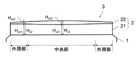
本発明において、前記薄膜は、その表層に前記表層を除く領域の薄膜よりも酸素含有量が多い酸化層を有する。図1に示すように、このマスクブランク3は、透光性基板1の主表面上に転写パターン形成用の薄膜2を備えた構成であり、薄膜2は、その表層に前記表層を除く領域の薄膜21よりも酸素含有量が多い酸化層22を有する。また、前記薄膜は、主表面側における外周部の厚さよりも中央部の厚さが厚く形成されている。図1に示すように、薄膜2は、主表面側における外周部の厚さHo2よりも中央部の厚さHc2が厚く形成されている。詳しくは、薄膜2は、薄膜の外周部から中央部に向かって膜厚が増加している。
In the present invention, the thin film has an oxide layer having a higher oxygen content than a thin film in a region excluding the surface layer. As shown in FIG. 1, the
ここで、図1においても、透光性基板の中心を基準とした一辺が所定長さの四角形を規定し、その四角形の内側の領域を中央部とし、その四角形の外側の領域を外周部としている。例えば、従来広く用いられているマスクブランクのサイズである、透光性基板の一辺が約152mmの方形状の場合、前記の四角形の一辺の長さは、例えば132mmや142mmとするとよい。なお、この四角形の一辺の長さはこれに限定されるものではない。また、中央部と外周部の境界線の形状は、四角形に限定されるものではない。特に、薄膜2の中央部の厚さHc2は、薄膜2の中央部の中心で測定された膜厚であると好ましい。また、薄膜2の外周部の厚さHo2は、薄膜2の外周部における内周部との境界線近傍で測定された膜厚であると好ましい。さらには、境界線が一辺が132mmの四角形状の場合、薄膜2の外周部の厚さHo2は、その四角形の角部近傍における薄膜2の外周部で測定された膜厚であるとより好ましい。
Here, also in FIG. 1, a side with a predetermined length as a reference with respect to the center of the translucent substrate is defined, a region inside the rectangle is a central portion, and a region outside the rectangle is an outer peripheral portion. Yes. For example, when the side of the translucent substrate having a square shape of about 152 mm, which is the size of a mask blank that has been widely used in the past, the length of one side of the square may be set to 132 mm or 142 mm, for example. Note that the length of one side of the square is not limited to this. Moreover, the shape of the boundary line between the central portion and the outer peripheral portion is not limited to a quadrangle. In particular, the thickness H c2 of the central portion of the
前記酸化層は、主表面側における外周部の厚さよりも中央部の厚さが厚く形成されている。図1に示すように、酸化層22は、主表面側における外周部の厚さHo22よりも中央部の厚さHc22が厚く形成されている。詳しくは、酸化層22は、薄膜の外周部から中央部に向かって膜厚が増加している。酸化層22の中央部の厚さHc22は、薄膜2の主表面側の中心で測定された膜厚であると好ましい。また、酸化層22の外周部の厚さHo22は、酸化層22の外周部における内周部との境界線近傍で測定された膜厚であると好ましい。さらには、境界線が一辺が132mmの四角形状の場合、酸化層22の外周部の厚さHo22は、その四角形の角部近傍における薄膜2の外周部で測定された膜厚であるとより好ましい。
The oxide layer is formed such that the thickness of the central portion is larger than the thickness of the outer peripheral portion on the main surface side. As shown in FIG. 1,
前記薄膜の主表面側における外周部および中央部の各膜厚と、前記酸化層の主表面側における外周部および中央部の各膜厚は、マスクブランクから転写用マスクを作製した後における、転写パターンが形成された薄膜(薄膜パターン)に求められる光学特性(露光光に対する透過率、露光光に与えるべき位相シフト量等)によって決定される。前記薄膜が、求められる光学特性を満たすことを前提条件として、その薄膜に形成される酸化層の膜厚の面内分布(前記酸化層の主表面側における外周部の膜厚Ho22と、および中央部の膜厚Hc22の差)と、その薄膜に酸化層が形成されることによって変わる光学特性の変化量から、透光性基板に薄膜を形成するときの膜厚分布(前記薄膜の主表面側における外周部の膜厚Ho2と、および中央部の膜厚Hc2)を決定する。 The film thicknesses of the outer peripheral part and the central part on the main surface side of the thin film and the film thicknesses of the outer peripheral part and the central part on the main surface side of the oxide layer are transferred after a transfer mask is prepared from a mask blank. It is determined by optical characteristics (transmittance to exposure light, phase shift amount to be given to exposure light, etc.) required for a thin film (thin film pattern) on which a pattern is formed. Assuming that the thin film satisfies the required optical properties, an in-plane distribution of the thickness of the oxide layer formed on the thin film (the thickness H o22 of the outer peripheral portion on the main surface side of the oxide layer, and The film thickness distribution when the thin film is formed on the light-transmitting substrate (main difference of the thin film) from the difference in the film thickness H c22 at the center) and the amount of change in the optical characteristics that changes when the oxide layer is formed on the thin film. The outer peripheral film thickness H o2 and the central film thickness H c2 ) on the surface side are determined.
本発明における転写パターン形成用の薄膜は、遷移金属Mとケイ素(Si)を含有し、さらに酸素(O)または窒素(N)のうち少なくともいずれかを含有する材料で形成されている。一般に、これらの材料からなる薄膜の表層に形成される酸化層は、ケイ素と酸素の含有量が多い層になる傾向が大きい。このような酸化層は、酸化層以外の薄膜の部分に比べて、透過率が高く(材料の消衰係数kが小さく)、透過する露光光に対して生じさせる位相シフト量が小さくなる(材料の屈折率nが小さくなる)。しかし、酸化層は、透過する露光光を多少減衰させ、透過する露光光の位相を多少シフトさせる。薄膜全体での主表面側における透過率分布と位相シフト量の分布の均一性を高くするには、酸化層による影響を無視するわけにはいかない。このため、透光性基板上に、最初に形成する薄膜の膜厚分布は、後工程でその薄膜の表層に形成される酸化層の膜厚分布とその酸化層が透過率や位相シフト量に与える影響を考慮して、決定する必要がある。よって、単純に、酸化層が形成された後、酸化層を除く薄膜の領域における外周部の膜厚(Ho21)と中央部の膜厚(Hc21)が同一になるように、薄膜の膜厚分布を選定すればよいというわけではない。なお、酸化層22を除く薄膜2の領域21における中央部の膜厚Hc21が、領域21における外周部の膜厚Ho21よりも薄くなる構成であると好ましい。
The thin film for forming a transfer pattern in the present invention contains a transition metal M and silicon (Si), and is formed of a material containing at least one of oxygen (O) and nitrogen (N). In general, an oxide layer formed on the surface layer of a thin film made of these materials tends to be a layer containing a large amount of silicon and oxygen. Such an oxide layer has a higher transmittance (a smaller extinction coefficient k of the material) than a thin film portion other than the oxide layer, and a smaller amount of phase shift to be generated for transmitted exposure light (material). The refractive index n of the However, the oxide layer slightly attenuates the transmitted exposure light and slightly shifts the phase of the transmitted exposure light. In order to increase the uniformity of the transmittance distribution and the phase shift amount distribution on the main surface side of the entire thin film, the influence of the oxide layer cannot be ignored. For this reason, the film thickness distribution of the thin film first formed on the light-transmitting substrate is the film thickness distribution of the oxide layer formed on the surface layer of the thin film in the subsequent process, and the oxide layer has a transmittance and phase shift amount. It is necessary to decide in consideration of the impact. Thus, simply, after the oxide layer has been formed, so that the film thickness of the central portion thickness of the outer peripheral portion in the region of the thin film except for the oxide layer (H o21) (H c21) are the same, thin film It is not necessary to select a thickness distribution. Incidentally, the central portion of the film thickness H c21 in the
前記酸化層は、自然酸化や転写用マスクの形での使用(露光光の長時間照射)で形成されたものは含まれない。薄膜の自然酸化や転写用マスクの形で使用していく中で薄膜パターンに形成されてしまう酸化層(以下、自然酸化等による酸化層という)は、表層の酸化が均等に進行する傾向が強い。このため、形成される表層の膜厚の均一性が比較的高く、構成1や構成6に係る発明のような膜厚分布の酸化層にはなり難い。よって、自然酸化等による酸化層だけを問題とする場合においては、薄膜を形成する工程において、主表面内で膜厚分布を変える必要性は低い。自然酸化等による酸化層だけを問題とする場合において、本発明のような薄膜の構成にすると、逆に光学特性の面内ばらつきが大きくなる恐れがある。 The oxide layer does not include those formed by natural oxidation or use in the form of a transfer mask (long exposure light exposure). Oxidation layer (hereinafter referred to as oxidation layer by natural oxidation, etc.) that is formed into a thin film pattern during use in the form of natural oxidation of a thin film or a transfer mask has a strong tendency to oxidize the surface layer evenly. . For this reason, the uniformity of the film thickness of the surface layer to be formed is relatively high, and it is difficult to become an oxide layer having a film thickness distribution as in the inventions according to the first and sixth structures. Therefore, when only the oxide layer by natural oxidation or the like is a problem, it is not necessary to change the film thickness distribution in the main surface in the process of forming the thin film. In the case where only the oxide layer formed by natural oxidation or the like is a problem, if the thin film is configured as in the present invention, the in-plane variation of the optical characteristics may be increased.
薄膜2において、中央部の厚さHc2と外周部の厚さHo2の比率は、前記薄膜の組成や、前記薄膜の透過率、前記薄膜の膜厚等との関係で一概に言えないが、例えば、Ho2/Hc2=0.94〜0.99の範囲が好ましく、0.95〜0.98の範囲であるとより好ましい。この場合において、酸化層22の中央部の厚さHc22と外周部の厚さHo22の比率は、例えば、Ho22/Hc22=0.17〜0.88の範囲が好ましく、0.25〜0.75の範囲であるとより好ましい。また、酸化層の膜厚は、最も厚い部分(中央部)でも4nm以下であることが好ましく、3nm以下であるとより好ましい。
In the
前記転写パターン形成用の薄膜は、遷移金属Mとケイ素(Si)を含有し、さらに酸素(O)または窒素(N)のうち少なくともいずれかを含有する材料からなる。遷移金属Mとしては、モリブデン(Mo)、タンタル(Ta)、タングステン(W)、チタン(Ti)、クロム(Cr)、ハフニウム(Hf)、ニッケル(Ni)、バナジウム(V)、ジルコニウム(Zr)、ルテニウム(Ru)、ロジウム(Rh)、ニオブ(Nb)、パラジウム(Pb)等の何れか一つまたは合金、などが挙げられる。前記転写パターン形成用の薄膜は、上記の成分に加え、炭素、水素、不活性ガス(ヘリウム,アルゴン,キセノン等)等を含有する材料からなる場合が含まれる。 The thin film for forming a transfer pattern is made of a material containing a transition metal M and silicon (Si) and further containing at least one of oxygen (O) and nitrogen (N). Transition metals M include molybdenum (Mo), tantalum (Ta), tungsten (W), titanium (Ti), chromium (Cr), hafnium (Hf), nickel (Ni), vanadium (V), zirconium (Zr). , Ruthenium (Ru), rhodium (Rh), niobium (Nb), palladium (Pb), etc., or an alloy thereof. The thin film for forming the transfer pattern includes a case of being made of a material containing carbon, hydrogen, inert gas (helium, argon, xenon, etc.) in addition to the above components.
前記転写パターン形成用の薄膜としては、さらに具体的には、遷移金属シリサイド、遷移金属シリサイド窒化物、遷移金属シリサイド窒化酸化物、遷移金属シリサイド酸化物、などが挙げられる。また、前記薄膜は、単層構造、多層構造を含む。前記薄膜は、反射防止層を含む態様であってもよい。前記薄膜は、組成傾斜膜を含む。 More specifically, examples of the transfer pattern forming thin film include transition metal silicide, transition metal silicide nitride, transition metal silicide nitride oxide, transition metal silicide oxide, and the like. The thin film includes a single layer structure and a multilayer structure. The thin film may include an antireflection layer. The thin film includes a composition gradient film.
前記薄膜は、半透過膜を含む。半透過膜は、単層構造、低透過率層と高透過率層とからなる2層構造、多層構造を含む。
また、半透過膜は、高透過率タイプを含む。高透過率タイプは、例えば、通常の透過率1〜10%未満に対し、相対的に高い透過率10〜30%を有するものをいう。
前記薄膜は、位相シフトマスクやエンハンサーマスクにおける半透過膜又は、バイナリマスクにおける遮光膜、とすることができる。バイナリマスクの遮光膜においても、EMFバイアスの観点で位相差の低減が要求されており、例えば、位相差の面内分布が厳密に問われる場合においては、本願発明の適用効果がある。
The thin film includes a semipermeable membrane. The semi-permeable membrane includes a single layer structure, a two-layer structure composed of a low transmittance layer and a high transmittance layer, and a multilayer structure.
The semi-permeable membrane includes a high transmittance type. The high transmittance type means, for example, a material having a relatively high transmittance of 10 to 30% with respect to a normal transmittance of less than 1 to 10%.
The thin film can be a semi-transmissive film in a phase shift mask or an enhancer mask, or a light shielding film in a binary mask. The light shielding film of the binary mask is also required to reduce the phase difference from the viewpoint of the EMF bias. For example, when the in-plane distribution of the phase difference is strictly asked, there is an effect of applying the present invention.
本発明において、前記遷移金属は、モリブデンであることが好ましい。前述したように、MoSiNやMoSiON等の材料からなる薄膜は、比較的大きな圧縮応力を有する傾向があり、圧縮応力を低減させるためには加熱処理が有効であり、本願課題が特に顕著になるからである。前記転写パターン形成用の薄膜としては、例えば、モリブデンシリサイド(MoSi)、モリブデンシリサイド窒化物(MoSiN)、モリブデンシリサイド窒化酸化物(MoSiNO)、モリブデンシリサイド酸化物(MoSiO)、モリブデンシリサイド窒化炭化物(MoSiCN)、モリブデンシリサイド酸化炭化物(MoSiOC)、モリブデンシリサイド酸化窒化炭化物(MoSiOCN)などが挙げられる。 In the present invention, the transition metal is preferably molybdenum. As described above, a thin film made of a material such as MoSiN or MoSiON tends to have a relatively large compressive stress, and heat treatment is effective for reducing the compressive stress. It is. Examples of the transfer pattern forming thin film include molybdenum silicide (MoSi), molybdenum silicide nitride (MoSiN), molybdenum silicide nitride oxide (MoSiNO), molybdenum silicide oxide (MoSiO), and molybdenum silicide nitride carbide (MoSiCN). Molybdenum silicide oxycarbide (MoSiOC), molybdenum silicide oxynitride carbide (MoSiOCN), and the like.
前記酸化層は、構成6にも記載されているように、薄膜に対して、酸素を含有する気体中で加熱処理と強制冷却処理を行う加熱冷却処理工程の過程で形成されることが好ましい。加熱処理で加熱した薄膜を強制冷却で急冷することにより、薄膜表層における酸素取り込み量の面内ばらつき度合いを制御しやすくなるためである。 As described in Structure 6, the oxide layer is preferably formed in the course of a heating / cooling process in which a heat treatment and a forced cooling process are performed on a thin film in a gas containing oxygen. This is because it is easy to control the degree of in-plane variation of the oxygen uptake amount in the surface layer of the thin film by quenching the thin film heated by the heat treatment by forced cooling.
本発明において、前記酸化層は、構成6に示すような加熱冷却処理工程によって形成されることが好ましい。この加熱冷却処理は、薄膜を有するマスクブランクに対し、酸素を含有する気体中で加熱処理を行い、かつ自然冷却される前に強制的に冷却する強制冷却処理を行うものである。加熱冷却処理工程によって形成される酸化層は、加熱処理時の加熱温度がより高い方が高い酸化度の被膜となり、マスクブランク製造時の洗浄処理で使用される洗浄液に対する耐性、このマスクブランクから転写用マスクを作製するプロセスで使用される洗浄液に対する耐性、転写用マスクを洗浄するときの洗浄液に対する耐性がそれぞれ高くなる。遷移金属とケイ素を含有する材料からなる薄膜の表層に各種洗浄耐性の高い酸化層を形成するには、少なくとも300℃以上の加熱温度で加熱処理することが必要とされる。また、薄膜への加熱処理は400℃以上の加熱温度が好ましく、より好ましくは450℃以上である。一方、薄膜への加熱処理の加熱温度は、透光性基板への影響を考慮すると、900℃以下であることが望ましい。 In the present invention, the oxide layer is preferably formed by a heating / cooling process as shown in Configuration 6. In this heating and cooling process, a mask blank having a thin film is subjected to a heating process in a gas containing oxygen, and a forced cooling process in which the mask blank is forcibly cooled before being naturally cooled. The higher the heating temperature during the heat treatment, the higher the degree of oxidation of the oxide layer formed by the heating / cooling process, and the resistance to the cleaning liquid used in the cleaning process during mask blank manufacturing, transfer from this mask blank. The resistance to the cleaning liquid used in the process of manufacturing the mask for printing and the resistance to the cleaning liquid when cleaning the transfer mask are increased. In order to form various oxide layers having high cleaning resistance on the surface layer of a thin film made of a material containing a transition metal and silicon, it is necessary to perform heat treatment at a heating temperature of at least 300 ° C. The heat treatment for the thin film is preferably performed at a heating temperature of 400 ° C. or higher, more preferably 450 ° C. or higher. On the other hand, the heating temperature of the heat treatment for the thin film is desirably 900 ° C. or lower in consideration of the influence on the light-transmitting substrate.
このような加熱冷却処理工程を複数枚のマスクブランクに対して同時に行うことを実現するには、前記の構成7に示したように、加熱冷却室内に、薄膜が形成された複数枚の透光性基板を、主表面を上下方向とし、かつ基板同士で間隔をおいて縦積みに配置し、加熱冷却室外であり、透光性基板の端面側(外周側)に加熱器と冷却器を配置し、加熱処理と強制冷却処理を行う工程とすることが好ましい。この工程を実現する加熱冷却装置としては、例えば、図3に示す縦型炉100が挙げられる。この縦型炉100は、石英チューブ10の内管10Bより内側の空間を加熱冷却室17としている。その加熱冷却室17内には、石英ボード16(石英でできた棚)が配置されている。この石英ボード16は、薄膜が形成された透光性基板(マスクブランク3)を、対向する主表面同士で互いに間隔をおいて配置することができるように、基板支持部16Aが設けられている。また、加熱冷却室17には、気体流入管13と気体流出管14が接続されている。加熱冷却処理工程中、酸素を含有する気体(空気等)を気体流入管13から流入させ、かつ気体流出管14から流出させ、加熱処理室17内の気体が常に入れ替わるようになっている。
In order to realize such a heating / cooling process step on a plurality of mask blanks simultaneously, as shown in the configuration 7, a plurality of light-transmitting sheets in which a thin film is formed in the heating / cooling chamber. The substrate is placed vertically with the main surface in the vertical direction, with the substrates spaced apart, outside the heating / cooling chamber, and the heater and cooler are placed on the end face side (outer peripheral side) of the translucent substrate It is preferable that the heat treatment and the forced cooling treatment be performed. An example of a heating / cooling apparatus that realizes this process is a
石英チューブ10は、外管10Aと内管10Bの2重管構造となっている。外管10Aには、冷媒管11,12が接続されている。この冷媒管11,12で、外管10Aの内壁と内管10Bの外壁に挟まれ空間に冷媒を流入・流出させることで、内管10Bの内部空間である加熱冷却室17を強制冷却させることができる。すなわち、石英チューブ10と冷媒管11,12と図示しない冷媒供給源によって、冷却器が構成されている。石英ボード16に配置されたマスクブランク3と冷媒との位置関係により、強制冷却処理はマスクブランク3の外周側から行われることになる。外管10Aの外周に加熱器として、ヒーター15が設けられている。石英ボード16に配置されたマスクブランク3とヒーター15との位置関係により、加熱処理もマスクブランク3の外周側から行われることになる。
The
加熱冷却処理における強制冷却処理は、加熱処理しているマスクブランクの薄膜が自然冷却で酸化層の形成に大きなばらつきが発生する温度に降下する前には少なくとも行われることが望まれる。前記の構成8に示したように、加熱冷却処理工程を、加熱器による加熱処理を行った後であり、かつ加熱冷却処理室内の温度が300℃以上のときに、冷却器による強制冷却処理を行う工程とすることが望ましい。ここでいう加熱処理を行った後とは、加熱処理の熱源である加熱器を停止した直後に限らず、加熱器を停止する直前に、冷却器による強制冷却を開始する工程も含まれる。前記薄膜に対する加熱処理および強制冷却処理は、薄膜の外周部から中央部に向かって加熱および冷却が進行するような加熱器および冷却器の配置が望ましい。このような加熱器および冷却器の配置とすることにより、加熱処理において、自然酸化に比べて酸素を膜中に取り込む速度が大幅に上昇する温度(約300℃)に達してから、強制冷却処理において、酸素を膜中に取り込む速度が大幅に低下する温度に薄膜の表面温度が低下するまでの時間が、薄膜の外周部に比べて中央部の方が長くすることができる。これにより、薄膜の表層に形成される酸化層の膜厚が、主表面側において、中央部が外周部に比べて厚くすることができる。 The forced cooling process in the heating and cooling process is desirably performed at least before the thin film of the mask blank being heated falls to a temperature at which large variations occur in the formation of the oxide layer due to natural cooling. As shown in the configuration 8, the heating / cooling process is performed after the heating process by the heater, and the forced cooling process by the cooler is performed when the temperature in the heating / cooling process chamber is 300 ° C. or higher. It is desirable that the process be performed. The term “after the heat treatment” is not limited to immediately after stopping the heater that is the heat source of the heat treatment, but includes a step of starting forced cooling by the cooler immediately before stopping the heater. In the heat treatment and forced cooling treatment for the thin film, it is desirable to arrange the heater and the cooler so that the heating and cooling proceed from the outer peripheral portion to the central portion of the thin film. By arranging such a heater and cooler, forced cooling treatment is performed after reaching a temperature (about 300 ° C.) at which the rate of taking oxygen into the film is significantly increased compared to natural oxidation in the heat treatment. In this case, the time until the surface temperature of the thin film is lowered to a temperature at which the rate of taking oxygen into the film is significantly reduced can be made longer in the central portion than in the outer peripheral portion of the thin film. Thereby, the film thickness of the oxide layer formed on the surface layer of the thin film can be thicker at the center portion than at the outer peripheral portion on the main surface side.
加熱処理中と、少なくとも酸素を膜中に取り込む速度が大幅に低下する温度に薄膜の表面温度が低下するまでの間の強制冷却処理中は、マスクブランクの薄膜の周囲には酸素を含有する気体が存在している必要がある。酸素を含有する気体としては、空気でもよいが、ケミカルフィルタを通したドライエアが好ましい。 A gas containing oxygen around the thin film of the mask blank during the heat treatment and during the forced cooling process until the surface temperature of the thin film is lowered to a temperature at which the rate at which oxygen is taken into the film is greatly reduced. Must exist. The gas containing oxygen may be air, but dry air that has passed through a chemical filter is preferable.
前記薄膜形成工程は、構成6に示すような透光性基板の主表面上に、遷移金属とケイ素を含有するターゲットを用い、酸素または窒素のうち少なくともいずれかを含有するスパッタリングガス中でスパッタリング法によって薄膜を形成する工程であることが好ましい。加熱冷却処理工程前の薄膜の主表面側における膜組成の均一性が高いことが望まれるため、枚葉式スパッタ装置で薄膜を形成することが好ましい。本発明における薄膜は、主表面側における膜厚分布を制御することは必要であるが、膜厚分布が均一にすることはなく、逆に外周部の膜厚を相対的に薄くする。このため、透光性基板の薄膜を形成する側の主表面の直上に対向してターゲット面を配置した構成の枚葉式スパッタ装置を用いることも可能である。 The thin film forming step uses a target containing a transition metal and silicon on the main surface of a light-transmitting substrate as shown in Configuration 6, and a sputtering method in a sputtering gas containing at least one of oxygen and nitrogen The step of forming a thin film by is preferable. Since it is desired that the uniformity of the film composition on the main surface side of the thin film before the heating / cooling process is high, it is preferable to form the thin film with a single wafer sputtering apparatus. Although it is necessary for the thin film in the present invention to control the film thickness distribution on the main surface side, the film thickness distribution is not made uniform, and conversely, the film thickness of the outer peripheral portion is made relatively thin. For this reason, it is also possible to use a single-wafer sputtering apparatus having a configuration in which a target surface is disposed directly above the main surface on the side where the thin film of the translucent substrate is formed.
一方、形成された薄膜の欠陥品質(パーティクルに起因する欠陥の低減)をより高めることを考慮すると、前記薄膜形成工程は、構成9のような、前記基板を主表面の中心を通る回転軸で回転させ、スパッタリングターゲットのスパッタ面を、前記基板の主表面と対向し、かつ前記主表面に対して所定の角度を有する位置であり、前記基板の回転軸と、前記スパッタ面の中心を通り前記基板の回転軸に対して平行な直線とがずれた位置に配置し、スパッタリング法によって前記薄膜を形成することが好ましい。より具体的には、前記の特開2002−090978号公報に開示されており、また図2にも示している斜入射スパッタ法式のスパッタ装置を適用することが好ましい。なお、この場合、形成された薄膜が本発明の膜厚分布になるように、ターゲット−基板間垂直距離(T/S)やオフセット距離を調整することが必要である。前記薄膜形成工程は、基板を回転させながら行うことが好ましい。基板を回転させない場合に比べ、薄膜の膜厚等を均一に成膜するためである。薄膜を形成する方法としては、DCスパッタ法、RFスパッタ法、イオンビームスパッタ法が適用可能である。特に、前記薄膜形成工程は、DCスパッタ法が好ましい。成膜速度が大きく、量産性に優れるためである。 On the other hand, in consideration of further improving the defect quality (reduction of defects caused by particles) of the formed thin film, the thin film forming step is performed by rotating the substrate with the rotation axis passing through the center of the main surface as in the configuration 9. The sputter surface of the sputtering target is a position facing the main surface of the substrate and having a predetermined angle with respect to the main surface, and passes through the rotation axis of the substrate and the center of the sputter surface. It is preferable to dispose the thin film by a sputtering method by disposing it at a position shifted from a straight line parallel to the rotation axis of the substrate. More specifically, it is preferable to apply a grazing incidence sputtering method sputtering apparatus disclosed in the aforementioned Japanese Patent Laid-Open No. 2002-090978 and also shown in FIG. In this case, it is necessary to adjust the target-substrate vertical distance (T / S) and the offset distance so that the formed thin film has the film thickness distribution of the present invention. The thin film forming step is preferably performed while rotating the substrate. This is because the film thickness of the thin film is uniformly formed as compared with the case where the substrate is not rotated. As a method for forming a thin film, a DC sputtering method, an RF sputtering method, or an ion beam sputtering method can be applied. In particular, the thin film forming step is preferably a DC sputtering method. This is because the deposition rate is high and the mass productivity is excellent.
本発明において、前記薄膜としては、構成2や構成10のような、露光光に対して1%以上の透過率を有する半透過膜が挙げられる。このような半透過膜としては、例えば、エンハンサーマスク作製用の位相差ゼロの半透過膜や、半透過膜のみでは位相シフト効果を生じさせるだけの位相差は得られないが、透光部の基板表面から所定深さだけ掘り込むことで位相シフト効果を生じさせる位相差が得られる位相シフトマスクを作製するための半透過膜が挙げられる。
In the present invention, examples of the thin film include a semi-transmissive film having a transmittance of 1% or more with respect to exposure light, such as
本発明において、前記薄膜としては、構成3および構成11のような、露光光に対して1%以上の透過率を有し、かつ、前記薄膜を透過した露光光と前記薄膜の膜厚と同じ距離だけ空気中を通過した露光光との間に位相シフト効果を生じさせる所定の位相差が得られるハーフトーン位相シフト膜が挙げられる。
In the present invention, the thin film has a transmittance of 1% or more with respect to exposure light as in the
本発明において、前記薄膜がバイナリマスクの遮光膜の場合、その膜厚は、65nm以下であることが好ましく、55nm以下であることがさらに好ましい。また、前記薄膜がハーフトーン位相シフトマスクのハーフトーン位相シフト膜の場合、その膜厚は、75nm以下であることが好ましく、70nm以下であることがさらに好ましい。また、前記薄膜がエンハンサーマスクの半透過膜の場合、その膜厚は、40nm以下であることが好ましく、30nm以下であることがさらに好ましい。 In the present invention, when the thin film is a light shielding film of a binary mask, the film thickness is preferably 65 nm or less, and more preferably 55 nm or less. When the thin film is a halftone phase shift film of a halftone phase shift mask, the film thickness is preferably 75 nm or less, and more preferably 70 nm or less. Moreover, when the said thin film is a semi-permeable film of an enhancer mask, the film thickness is preferably 40 nm or less, and more preferably 30 nm or less.
本発明において、前記薄膜は、構成4、および構成12に示すような、前記透過率の面内分布が0.6%の範囲内であることが好ましい。例えば、透過率の目標値に対して面内各所の透過率が、+0.6%の範囲内である場合、−0.6%の範囲内である場合、透過率の目標値に対して面内各所の透過率の最大値および最小値が±0.3%の範囲内にある場合、であれば、前記透過率の面内分布は0.6%の範囲内となる。前記薄膜は、透過率の目標値に対して面内各所の透過率(透過率の最大値および最小値)が±0.3%の範囲内にあることが、さらに好ましい。
In the present invention, it is preferable that the thin film has an in-plane distribution of the transmittance within a range of 0.6% as shown in
本発明において、前記薄膜は、構成5および構成13に示すような、前記位相差の面内分布が4度の範囲内であることが好ましい。例えば、位相差の目標値に対して面内各所の位相差が、+4度の範囲内である場合、−4度の範囲内である場合、位相差の目標値に対して面内各所の位相差の最大値および最小値が±2度の範囲内にある場合、であれば、前記位相差の面内分布は4度の範囲内となる。前記薄膜は、位相差の目標値に対して面内各所の位相差(位相差の最大値および最小値)が±2度の範囲内にあることが、さらに好ましい。
In the present invention, it is preferable that the thin film has an in-plane distribution of the phase difference within a range of 4 degrees as shown in
本発明の転写用マスクは、構成14に示すように、構成1から5のいずれかに記載のマスクブランクの前記薄膜に転写パターンが形成されていることを特徴とする。
As shown in
本発明の転写用マスクの製造方法は、構成15に示すように、構成6から13のいずれかに記載のマスクブランク製造方法で製造されたマスクブランクの前記薄膜に転写パターンを形成するパターン形成工程を有することを特徴とする。
The transfer mask manufacturing method of the present invention includes a pattern forming step of forming a transfer pattern on the thin film of the mask blank manufactured by the mask blank manufacturing method according to any one of configurations 6 to 13, as shown in
本発明において、マスクブランクから転写用マスクを作製する際に、マスクブランクの薄膜上に形成されるレジストは、化学増幅型レジストであることが好ましい。高精度の加工に適するためである。また、レジストは電子線描画用のレジストであることが好ましい。高精度の加工に適するためである。
本発明は、電子線描画によりレジストパターンを形成する電子線描画用のマスクブランクに適用する。
In the present invention, when a transfer mask is produced from a mask blank, the resist formed on the thin film of the mask blank is preferably a chemically amplified resist. This is because it is suitable for high-precision processing. The resist is preferably an electron beam drawing resist. This is because it is suitable for high-precision processing.
The present invention is applied to a mask blank for electron beam drawing in which a resist pattern is formed by electron beam drawing.
本発明において、透光性基板は、使用する露光波長に対して透明性を有するものであれば特に制限されない。本発明では、石英基板、その他各種のガラス基板(例えば、CaF2基板、ソーダライムガラス、無アルカリガラス基板、アルミノシリケートガラス等)を用いることができるが、この中でも石英基板は、ArFエキシマレーザーの波長領域で透明性が高いので、本発明には特に好適である。 In the present invention, the translucent substrate is not particularly limited as long as it has transparency with respect to the exposure wavelength to be used. In the present invention, a quartz substrate and other various glass substrates (for example, CaF 2 substrate, soda lime glass, non-alkali glass substrate, aluminosilicate glass, etc.) can be used. Among them, the quartz substrate is an ArF excimer laser. Since it has high transparency in the wavelength region, it is particularly suitable for the present invention.
本発明において、転写用マスクには、位相シフトマスク、位相シフト効果を使用しないバイナリマスク、が含まれる。転写用マスクには、レチクルが含まれる。位相シフトマスクには、ハーフトーン型(トライトーン型)等の位相シフトマスク、エンハンサーマスクが含まれる。 In the present invention, the transfer mask includes a phase shift mask and a binary mask that does not use the phase shift effect. The transfer mask includes a reticle. The phase shift mask includes a phase shift mask such as a halftone type (tritone type) and an enhancer mask.
本発明においては、前記半透過膜及びそのパターンの他に、他の薄膜及びそのパターンを形成できる。例えば、前記半透過膜の上又は下に遮光膜を有する形態の場合には、前記半透過膜の材料が遷移金属シリサイドを含むので、遮光膜の材料は、前記半透過膜に対してエッチング選択性を有する(エッチング耐性を有する)クロムや、クロムに酸素、窒素、炭素などの元素を添加したクロム化合物で構成することができる。これにより、光半透過膜パターンの上又は下に遮光膜パターンを形成できる。このクロムを含有する材料としては、クロム単体(Cr)の他、クロム(Cr)に窒素(N)、酸素(O)、炭素(C)、水素(H)、ヘリウム(He)などの元素を一以上含有する材料が含まれる。例えば、Cr、CrN、CrO、CrNO、CrNC、CrCONなどや、これらに加え水素(H)、ヘリウム(He)をそれぞれ含有する材料が含まれる。 In the present invention, in addition to the semipermeable membrane and its pattern, other thin films and their patterns can be formed. For example, in the case where the light-shielding film is provided above or below the semi-transmissive film, the material of the semi-transmissive film includes a transition metal silicide. Chrome (having etching resistance) or a chromium compound in which elements such as oxygen, nitrogen, and carbon are added to chromium. Thereby, the light shielding film pattern can be formed on or below the light semi-transmissive film pattern. The chromium-containing material includes chromium (Cr), chromium (Cr), nitrogen (N), oxygen (O), carbon (C), hydrogen (H), helium (He), and other elements. Materials containing one or more are included. For example, Cr, CrN, CrO, CrNO, CrNC, CrCON, etc., and materials containing hydrogen (H) and helium (He) in addition to these are included.
本発明において、遷移金属とケイ素を含む薄膜のドライエッチングには、例えば、SF6、CF4、C2F6、CHF3等の弗素系ガス、これらとHe、H2、N2、Ar、C2H4、O2等の混合ガスを用いることができる。また、クロム系薄膜のドライエッチングには、塩素系ガスと酸素ガスとを含む混合ガスからなるドライエッチングガスを用いることができる。ドライエッチングに用いる塩素系ガスとしては、例えば、Cl2、SiCl4、HCl、CCl4、CHCl3等が挙げられる。 In the present invention, dry etching of a thin film containing a transition metal and silicon includes, for example, fluorine-based gases such as SF 6 , CF 4 , C 2 F 6 , CHF 3 , and these, and He, H 2 , N 2 , Ar, A mixed gas such as C 2 H 4 or O 2 can be used. For dry etching of the chromium-based thin film, a dry etching gas composed of a mixed gas containing a chlorine-based gas and an oxygen gas can be used. Examples of the chlorine-based gas used for dry etching include Cl 2 , SiCl 4 , HCl, CCl 4 , and CHCl 3 .
一方、本発明のマスクブランクでは、透光性基板上に設けられる転写パターン形成用の薄膜は、遷移金属とケイ素を含有し、さらに酸素または窒素のうち少なくともいずれかを含有する材料で形成される。しかし、ケイ素と窒素からなる材料、またはケイ素と窒素からなる材料に半金属元素、非金属元素および希ガスから選ばれる1以上の元素を含有する材料を、本発明のパターン形成用の薄膜を形成する材料に用いた場合においても、本発明のパターン形成用の薄膜の構成を適用することができ、同様の効果を得ることができる。 On the other hand, in the mask blank of the present invention, the transfer pattern forming thin film provided on the light-transmitting substrate is formed of a material containing a transition metal and silicon, and further containing at least one of oxygen and nitrogen. . However, a thin film for forming a pattern according to the present invention is formed using a material comprising silicon and nitrogen, or a material comprising one or more elements selected from a metalloid element, a nonmetallic element and a rare gas in a material comprising silicon and nitrogen. Even when it is used as the material to be used, the configuration of the thin film for pattern formation of the present invention can be applied, and the same effect can be obtained.
具体的な構成としては、透光性基板の主表面上に、転写パターン形成用の薄膜を備えたマスクブランクであって、前記薄膜は、ケイ素と窒素からなる材料、またはケイ素と窒素からなる材料に半金属元素、非金属元素および希ガスから選ばれる1以上の元素を含有する材料からなり、前記薄膜は、その表層に前記表層を除く領域の薄膜よりも酸素含有量が多い酸化層を有し、前記薄膜は、主表面側における外周部の厚さよりも中央部の厚さが厚く形成されており、前記酸化層は、主表面側における外周部の厚さよりも中央部の厚さが厚く形成されているマスクブランクである。 As a specific configuration, a mask blank provided with a thin film for forming a transfer pattern on a main surface of a translucent substrate, wherein the thin film is a material composed of silicon and nitrogen, or a material composed of silicon and nitrogen. In addition, the thin film has an oxide layer having a higher oxygen content than the thin film in the region excluding the surface layer on the surface layer thereof, which includes at least one element selected from a metalloid element, a nonmetallic element, and a rare gas. The thin film is formed so that the thickness of the central portion is larger than the thickness of the outer peripheral portion on the main surface side, and the thickness of the central portion is thicker than the thickness of the outer peripheral portion on the main surface side. It is the mask blank currently formed.
ケイ素と窒素からなる材料等を適用した転写パターン形成用の薄膜の場合でも、屈折率と消衰係数が高い元素である遷移金属を含有している本発明の転写パターン形成用の薄膜ほどではないが、加熱冷却処理によって薄膜の表層に形成される酸化層の膜厚分布が均一でないことで、薄膜全体での透過率分布や位相シフト量の分布の均一性が低下することが生じる。よって、ケイ素と窒素からなる材料等を適用した転写パターン形成用の薄膜の場合でも、薄膜と酸化層の各厚さを本発明に規定する構成とすることで、薄膜全体での透過率分布や位相シフト量の分布の均一性を高めることができる。 Even in the case of a thin film for forming a transfer pattern using a material comprising silicon and nitrogen, it is not as thin as the thin film for forming a transfer pattern of the present invention containing a transition metal which is an element having a high refractive index and extinction coefficient. However, since the film thickness distribution of the oxide layer formed on the surface layer of the thin film by the heating and cooling process is not uniform, the uniformity of the transmittance distribution and the phase shift amount distribution in the entire thin film is deteriorated. Therefore, even in the case of a thin film for forming a transfer pattern to which a material composed of silicon and nitrogen is applied, the transmittance distribution in the entire thin film and The uniformity of the phase shift amount distribution can be improved.
同様に、本発明のマスクブランクの製造方法においても、薄膜形成工程を、ケイ素ターゲットまたはケイ素に半金属元素および非金属元素から選ばれる1以上の元素を含有する材料からなるターゲットを用い、窒素系ガスと希ガスを含むスパッタリングガス中でのスパッタリング法によって、薄膜を形成する工程に代えた場合においても、本発明のマスクブランクの製造方法で得られる効果と同様の効果を得ることができる。 Similarly, also in the mask blank manufacturing method of the present invention, the thin film forming step is performed using a silicon target or a target made of a material containing one or more elements selected from a semi-metal element and a non-metal element in silicon. Even when the thin film is formed by a sputtering method in a sputtering gas containing a gas and a rare gas, the same effect as that obtained by the mask blank manufacturing method of the present invention can be obtained.
具体的な構成としては、透光性基板の主表面上に、転写パターン形成用の薄膜を備えたマスクブランクの製造方法であって、前記透光性基板の主表面上に、ケイ素ターゲットまたはケイ素に半金属元素および非金属元素から選ばれる1以上の元素を含有する材料からなるターゲットを用い、窒素系ガスと希ガスを含むスパッタリングガス中でスパッタリング法により前記薄膜を形成する薄膜形成工程と、前記薄膜形成工程で形成した前記薄膜に対し、酸素を含有する気体中で加熱処理および強制冷却処理を行う加熱冷却処理工程とを有し、前記薄膜形成工程は、前記薄膜を主表面側おける外周部の厚さよりも中央部の厚さを厚くなるように形成する工程であり、前記加熱冷却処理工程は、前記薄膜の表層にその表層を除く領域の薄膜よりも酸素含有量が多い酸化層を形成する工程であり、かつ前記酸化層を主表面側における外周部の厚さよりも中央部の厚さが厚くなるように形成する工程であるマスクブランクの製造方法である。 As a specific configuration, a mask blank manufacturing method including a transfer pattern forming thin film on a main surface of a translucent substrate, wherein a silicon target or silicon is formed on the main surface of the translucent substrate. A thin film forming step of forming the thin film by a sputtering method in a sputtering gas containing a nitrogen-based gas and a rare gas, using a target made of a material containing one or more elements selected from metalloid elements and nonmetallic elements; The thin film formed in the thin film forming step has a heating / cooling treatment step in which a heat treatment and a forced cooling treatment are performed in a gas containing oxygen, and the thin film forming step includes an outer periphery on the main surface side. The thickness of the central portion is larger than the thickness of the portion, and the heating and cooling treatment step is more acidic than the thin film in the region excluding the surface layer on the surface layer of the thin film. A mask blank manufacturing method, which is a step of forming an oxide layer having a large content and a step of forming the oxide layer so that the thickness of the central portion is larger than the thickness of the outer peripheral portion on the main surface side. .
前記薄膜に含有する半金属元素は、特に限定されない。半金属元素の中でも、ホウ素、ゲルマニウム、アンチモンおよびテルルから選ばれる一以上の元素を含有させるようにすると、スパッタリングターゲットとして用いるケイ素にこれらの半金属元素を含有させることができ、ターゲットの導電性を高めることが期待できるため、好ましい。このマスクブランクの製造方法における薄膜形成工程では、いずれのスパッタリング法も適用できる。ターゲットの導電性が、遷移金属を含有させた薄膜の場合に比べて低いことから、RFスパッタ法やイオンビームスパッタ法を適用するとより好ましい。 The metalloid element contained in the thin film is not particularly limited. Among metalloid elements, when one or more elements selected from boron, germanium, antimony and tellurium are included, silicon used as a sputtering target can contain these metalloid elements, and the conductivity of the target can be increased. It is preferable because it can be expected to increase. Any sputtering method can be applied in the thin film forming step in the mask blank manufacturing method. Since the conductivity of the target is lower than that of a thin film containing a transition metal, it is more preferable to apply an RF sputtering method or an ion beam sputtering method.
前記薄膜には、いずれの非金属元素を含有させてもよい。非金属元素の中でも、炭素、フッ素および水素から選ばれる一以上の元素を含有させると好ましい。前記薄膜形成工程で使用する窒素系ガスは、窒素を含有するガスであればいずれのガスも適用可能である。酸化層が形成される前の前記薄膜は酸素含有量を低く抑えることが好ましいため、酸素を含有しない窒素系ガスを適用することが好ましく、窒素ガスを適用するとより好ましい。前記薄膜形成工程で使用する希ガスは、いずれの希ガスも適用可能であるが、成膜レートのことを考慮すると、アルゴン、クリプトン、キセノンを適用することが好ましい。また、形成される薄膜の応力を緩和することを考慮すると、原子量の小さいヘリウム、ネオンを適用し、薄膜に積極的に取り込ませることが好ましい。 The thin film may contain any nonmetallic element. Among nonmetallic elements, it is preferable to contain one or more elements selected from carbon, fluorine and hydrogen. As the nitrogen-based gas used in the thin film forming step, any gas can be applied as long as it contains nitrogen. Since it is preferable to keep the oxygen content low in the thin film before the oxide layer is formed, it is preferable to apply a nitrogen-based gas not containing oxygen, and more preferable to apply nitrogen gas. Any rare gas can be used as the rare gas used in the thin film formation step, but it is preferable to use argon, krypton, or xenon in consideration of the film formation rate. In consideration of relieving the stress of the thin film to be formed, it is preferable to apply helium and neon having a small atomic weight to actively take in the thin film.
なお、遷移金属を含有しない材料で形成されている薄膜を有する前記のマスクブランクやそのマスクブランクの製造方法に関するその他の構成については、本発明のマスクブランクや本発明のマスクブランクの製造方法の場合と同様である。また、遷移金属を含有しない材料で形成されている薄膜を有する前記のマスクブランクを用いて作製される転写用マスクやその転写用マスクの製造方法についても、本発明の転写用マスクや本発明の転写用マスクの製造方法と同様である。 In addition, about the other structure regarding the manufacturing method of the said mask blank which has the thin film formed with the material which does not contain a transition metal, and its mask blank, the case of the manufacturing method of the mask blank of this invention or the mask blank of this invention It is the same. Further, regarding the transfer mask produced using the mask blank having the thin film formed of a material not containing a transition metal and the method for producing the transfer mask, the transfer mask of the invention and the transfer mask of the invention are also used. This is the same as the manufacturing method of the transfer mask.
以下、実施例に基づき、本発明をさらに具体的に説明する。 Hereinafter, based on an Example, this invention is demonstrated further more concretely.
(実施例1)
透光性基板として、主表面が約152mm×約152mmの四角形であり、厚さが約6.25mmの合成石英ガラス基板を用い、その透光性基板上に、モリブデン、シリコン、および窒素からなる半透過膜(薄膜)を成膜した。半透過膜の成膜には、図2に示す、いわゆる斜入射スパッタ方式かつ枚葉処理方式のDCスパッタリング装置を使用した。具体的には、モリブデン(Mo)とシリコン(Si)との混合ターゲット(Mo:Si=12at%:88at%)を用い、アルゴン(Ar)と窒素(N2)とヘリウム(He)との混合ガス雰囲気(ガス流量比 Ar:N2:He=8:72:100)で、反応性スパッタリング(DCスパッタリング)により、透光性基板上に、モリブデン、シリコン及び窒素からなるMoSiN膜(位相シフト膜)を形成した。このとき、形成される半透過膜の平均膜厚が69nmであり、かつ中央部の膜厚が外周部の膜厚に比べて18Å程度厚くなるように、DCスパッタリング装置の成膜条件(T/S距離、オフセット距離、スパッタ電圧の諸条件)を設定した。ここで、形成される薄膜の中央部と外周部の境界は、合成石英ガラス基板の中心を基準とした一辺が132mmの四角形とした。また、その境界から内側の領域を中央部とし、その境界から外側の領域を外周部とした。なお、ここでは、酸化層形成後における位相シフト膜(マスクブランクが完成したときの位相シフト膜)が、ArFエキシマレーザーの波長193nmの露光光に対する透過率が6%であり、かつ位相シフト量が177度になるように成膜条件を設定した。
Example 1
As the translucent substrate, a synthetic quartz glass substrate having a main surface of a square of about 152 mm × about 152 mm and a thickness of about 6.25 mm is used. The translucent substrate is made of molybdenum, silicon, and nitrogen. A semi-permeable membrane (thin film) was formed. For the formation of the semi-transmissive film, a so-called oblique incidence sputtering type and single wafer processing type DC sputtering apparatus shown in FIG. 2 was used. Specifically, using a mixed target of molybdenum (Mo) and silicon (Si) (Mo: Si = 12 at%: 88 at%), mixing argon (Ar), nitrogen (N 2 ), and helium (He) MoSiN film (phase shift film) made of molybdenum, silicon and nitrogen on a light-transmitting substrate by reactive sputtering (DC sputtering) in a gas atmosphere (gas flow ratio Ar: N 2 : He = 8: 72: 100). ) Was formed. At this time, the film forming conditions (T / T) of the DC sputtering apparatus are set such that the average thickness of the semi-transmissive film to be formed is 69 nm and the thickness of the central portion is about 18 mm thicker than the thickness of the outer peripheral portion. Various conditions of S distance, offset distance, and sputtering voltage) were set. Here, the boundary between the central portion and the outer peripheral portion of the thin film to be formed was a quadrangle having a side of 132 mm with respect to the center of the synthetic quartz glass substrate. Moreover, the area | region inside from the boundary was made into the center part, and the area | region outside the boundary was made into the outer peripheral part. Here, the phase shift film after forming the oxide layer (the phase shift film when the mask blank is completed) has an ArF excimer laser transmittance of 6% for exposure light with a wavelength of 193 nm, and the phase shift amount is The film forming conditions were set to 177 degrees.
形成されたMoSiN膜(位相シフト膜)について、薄膜の中央部(透光性基板の主表面の中心)に対して、位相シフト量測定装置(レーザーテック社製 MPM193)でArFエキシマレーザーの波長である波長193nmの光に対する透過率と位相シフト量をそれぞれ測定したところ、透過率が4.52%、位相シフト量が182.5度であった。また、位相シフト膜の中央部の膜厚として、透光性基板の主表面の中心の膜厚をX線反射率法(XRR)で測定したところ、702Åであった。位相シフト膜の外周部の平均膜厚として、境界の四角形における4つの角部近傍の各外周部の膜厚をX線反射率法(XRR)で測定し、平均値を算出たところ、684Åであった。なお、X線反射率法の測定では、リガク社製 GXR300RDを使用した。 About the formed MoSiN film (phase shift film), it is a wavelength of ArF excimer laser with a phase shift amount measuring device (MPM193 manufactured by Lasertec Co., Ltd.) with respect to the central part of the thin film (center of the main surface of the translucent substrate). When the transmittance and phase shift amount with respect to light having a wavelength of 193 nm were measured, the transmittance was 4.52% and the phase shift amount was 182.5 degrees. Further, the film thickness at the center of the main surface of the translucent substrate as measured at the center of the phase shift film was 702 mm when measured by the X-ray reflectivity method (XRR). As the average film thickness of the outer peripheral part of the phase shift film, the film thickness of each outer peripheral part in the vicinity of the four corners in the boundary rectangle was measured by the X-ray reflectivity method (XRR), and the average value was calculated. there were. In the measurement by the X-ray reflectivity method, GXR300RD manufactured by Rigaku Corporation was used.
次に、同様の手順で5枚作成したMoSiN膜(位相シフト膜)を成膜した透光性基板を、図3の縦型炉100の石英ボードの各段の基板支持部16Aに間隔をおいて縦積みに載置した。ここで、石英ボードの最上段と最下段の基板支持部16Aには、位相シフト膜が成膜されていない透光性基板(ダミー基板)を載置した。これは、最上段と最下段は、外乱等の影響を受けやすく、酸化層の膜厚を制御することが難しいためである。薄膜への加熱処理は、ヒーター(加熱器)15で加熱し始めてから加熱冷却室17内の温度が450℃に達したときから1時間行われた。そして、ヒーター15からの加熱を停止した直後から、冷媒管11から冷媒を注入し始め、加熱冷却室17内を常温になるまで強制的に冷却することで、薄膜への強制冷却処理を行った。この加熱処理および強制冷却処理によって、MoSiN膜(位相シフト膜)の表層に酸化層を形成した。
Next, the translucent substrate on which five MoSiN films (phase shift films) prepared in the same procedure are formed is spaced from the
強制冷却処理後の位相シフト膜を備える透光性基板5枚に対して、同様に波長193nmの光に対する透過率と位相シフト量を測定した。薄膜の中央部(透光性基板の主表面の中心)の測定結果は、透過率が平均6.16%、位相シフト量が平均178.1度であった。また、位相シフト膜の外周部である酸化層の形成前に膜厚を測定した4箇所の外周部で、同様に透過率と位相シフト量をそれぞれ測定し、透過率の平均値と位相シフト量の平均値を算出した。その結果、位相シフト膜の外周部における平均透過率が6.07%、平均位相シフト量が177.3であった。また、5枚の強制冷却処理後の位相シフト膜を備える透光性基板は、薄膜の中央部、外周部ともに、透過率の測定値が、設計透過率の6%から±0.3%の範囲内に収まっていた。同時に、5枚のマスクブランクは、位相シフト膜の中央部、外周部ともに、位相シフト量の測定値が、設計位相シフト量の177度から±2度の範囲内に収まっていた。 Similarly, the transmittance and phase shift amount with respect to light having a wavelength of 193 nm were measured for five light-transmitting substrates including the phase shift film after the forced cooling treatment. The measurement results at the center of the thin film (the center of the main surface of the translucent substrate) showed an average transmittance of 6.16% and an average phase shift amount of 178.1 degrees. Further, the transmittance and the phase shift amount were measured in the same manner at the four outer peripheral portions where the film thickness was measured before the formation of the oxide layer, which is the outer peripheral portion of the phase shift film, and the average value of the transmittance and the phase shift amount were measured. The average value of was calculated. As a result, the average transmittance at the outer peripheral portion of the phase shift film was 6.07%, and the average phase shift amount was 177.3. In addition, the translucent substrate provided with the five phase-shifted films after forced cooling treatment has a measured transmittance of 6% to ± 0.3% of the designed transmittance at both the central portion and the outer peripheral portion of the thin film. It was within the range. At the same time, in the five mask blanks, the measured value of the phase shift amount was within the range of the design phase shift amount of 177 degrees to ± 2 degrees in both the central portion and the outer peripheral portion of the phase shift film.
さらに、この強制冷却処理後の位相シフト膜を備える透光性基板に対して、X線反射率法(XRR)を用いて、酸化層の膜厚を測定した。その結果、位相シフト膜の中央部が外周部よりも酸化層の膜厚が厚かった。また、外周部と中央部の膜厚の差は、平均で15Åであった。 Furthermore, the film thickness of the oxide layer was measured using the X-ray reflectivity method (XRR) with respect to the translucent board | substrate provided with the phase shift film | membrane after this forced cooling process. As a result, the central portion of the phase shift film was thicker than the outer peripheral portion. The difference in film thickness between the outer peripheral part and the central part was 15 mm on average.
(比較例1)
実施例1と同様に、透光性基板上に、モリブデン、シリコン、および窒素からなる半透過膜(薄膜)を成膜した。ただし、この比較例では、DCスパッタリング装置で半透過膜を成膜する際、膜厚が主表面側で出来る限り均一になるような成膜条件を適用した。このため、透光性基板上に形成されたMoSiN膜(位相シフト膜)は、外周部と中央部の膜厚差が5Å程度と、実施例1に比べると大幅に小さかった。同様の手順で比較例1のMoSiN膜(位相シフト膜)を成膜した透光性基板を5枚作成した。さらに比較例1の位相シフト膜を有する透光性基板5枚に対して、実施例1と同条件で加熱処理および強制冷却処理を行った。この加熱処理および強制冷却処理を行ったことにより、MoSiN膜(位相シフト膜)の表層に酸化層を形成されていた。
(Comparative Example 1)
Similar to Example 1, a semi-transmissive film (thin film) made of molybdenum, silicon, and nitrogen was formed on a light-transmitting substrate. However, in this comparative example, when forming a semi-transmissive film with a DC sputtering apparatus, film forming conditions were applied so that the film thickness was as uniform as possible on the main surface side. For this reason, the MoSiN film (phase shift film) formed on the translucent substrate had a film thickness difference of about 5 mm between the outer peripheral portion and the central portion, which was significantly smaller than that of Example 1. In the same procedure, five translucent substrates on which the MoSiN film (phase shift film) of Comparative Example 1 was formed were prepared. Furthermore, the heat treatment and the forced cooling treatment were performed on the five light-transmitting substrates having the phase shift film of Comparative Example 1 under the same conditions as in Example 1. By performing this heat treatment and forced cooling treatment, an oxide layer was formed on the surface layer of the MoSiN film (phase shift film).
強制冷却処理後の位相シフト膜を備える透光性基板5枚に対して、同様に波長193nmの光に対する透過率と位相シフト量を測定した。薄膜の中央部(透光性基板の主表面の中心)の測定結果は、透過率が6.44%、位相シフト量が174.3度であった。また、位相シフト膜の外周部である酸化層の形成前に膜厚を測定した4箇所の外周部で、同様に透過率と位相シフト量をそれぞれ測定し、透過率の平均値と位相シフト量の平均値を算出した。その結果、位相シフト膜の外周部における平均透過率が5.72%、平均位相シフト量が180.1であった。また、5枚の強制冷却処理後の位相シフト膜を備える透光性基板は、薄膜の中央部、外周部ともに、透過率の測定値が、設計透過率の6%から±0.3%の範囲外となってしまっていた。同時に、5枚のマスクブランクは、位相シフト膜の中央部、外周部ともに、位相シフト量の測定値が、設計位相シフト量の177度から±2度の範囲外となってしまっていた。 Similarly, the transmittance and phase shift amount with respect to light having a wavelength of 193 nm were measured for five light-transmitting substrates including the phase shift film after the forced cooling treatment. As a result of measurement at the center of the thin film (center of the main surface of the light-transmitting substrate), the transmittance was 6.44% and the phase shift amount was 174.3 degrees. Further, the transmittance and the phase shift amount were measured in the same manner at the four outer peripheral portions where the film thickness was measured before the formation of the oxide layer, which is the outer peripheral portion of the phase shift film, and the average value of the transmittance and the phase shift amount were measured. The average value of was calculated. As a result, the average transmittance at the outer periphery of the phase shift film was 5.72%, and the average phase shift amount was 180.1. In addition, the translucent substrate provided with the five phase-shifted films after forced cooling treatment has a measured transmittance of 6% to ± 0.3% of the designed transmittance at both the central portion and the outer peripheral portion of the thin film. It was out of range. At the same time, in the five mask blanks, the measured value of the phase shift amount was outside the range of the designed phase shift amount of 177 degrees to ± 2 degrees in both the central portion and the outer peripheral portion of the phase shift film.
(位相シフトマスクの作製)
上記実施例1で製造した位相シフトマスクブランクの位相シフト膜上に、クロムを含有する材料からなる遮光膜を成膜し、遮光膜を有する位相シフトマスクブランクを作製した。成膜した遮光膜は、位相シフト膜側からCrCON膜(膜厚30nm)、CrN膜(膜厚4nm)、CrOCN膜(膜厚14nm)が順に積層した構造とした。このMoSiNからなる位相シフト膜とCr系材料からなる遮光膜の積層構造で、ArFエキシマレーザーの波長(193nm)に対する光学濃度は3.1であった。
(Production of phase shift mask)
A light shielding film made of a material containing chromium was formed on the phase shift film of the phase shift mask blank produced in Example 1 to prepare a phase shift mask blank having a light shielding film. The formed light shielding film has a structure in which a CrCON film (film thickness of 30 nm), a CrN film (film thickness of 4 nm), and a CrOCN film (film thickness of 14 nm) are sequentially laminated from the phase shift film side. In the laminated structure of the phase shift film made of MoSiN and the light shielding film made of Cr-based material, the optical density with respect to the wavelength (193 nm) of the ArF excimer laser was 3.1.
この作製した遮光膜を有する位相シフトマスクブランクを用いてハーフトーン型位相シフトマスクを作製した。具体的には、まず、マスクブランクの遮光膜上に、レジスト膜として、電子線描画用化学増幅型ポジレジスト膜(富士フィルムエレクトロニクスマテリアルズ社製 PRL009)を形成した。レジスト膜の形成は、スピンナー(回転塗布装置)を用いて、回転塗布した。 A halftone phase shift mask was produced using the produced phase shift mask blank having a light shielding film. Specifically, first, a chemically amplified positive resist film for electron beam drawing (PRL009 manufactured by Fuji Film Electronics Materials Co., Ltd.) was formed as a resist film on the light shielding film of the mask blank. The resist film was formed by spin coating using a spinner (rotary coating apparatus).
次に上記マスクブランク上に形成されたレジスト膜に対し、電子線描画装置を用いて位相シフト膜に形成すべき転写パターンの描画を行った後、所定の現像液で現像してレジストパターンを形成した。
続いて、上記レジストパターンをマスクとして、遮光膜のエッチングを行って遮光膜パターンを形成した。ドライエッチングガスとして、Cl2とO2の混合ガスを用いた。
次に、上記レジストパターンまたは遮光膜パターンをマスクとして、位相シフト膜のエッチングを行って位相シフトパターンを形成した。ドライエッチングガスとして、SF6とHeの混合ガスを用いた。
Next, a transfer pattern to be formed on the phase shift film is drawn on the resist film formed on the mask blank using an electron beam drawing apparatus, and then developed with a predetermined developer to form a resist pattern. did.
Subsequently, using the resist pattern as a mask, the light shielding film was etched to form a light shielding film pattern. A mixed gas of Cl 2 and O 2 was used as a dry etching gas.
Next, using the resist pattern or the light shielding film pattern as a mask, the phase shift film was etched to form a phase shift pattern. A mixed gas of SF 6 and He was used as the dry etching gas.
次に、残存するレジストパターンを除去し、電子線描画用化学増幅型ポジレジスト膜(富士フィルムエレクトロニクスマテリアルズ社製 PRL009)を回転塗布により、新たに形成した。さらに、形成したレジスト膜に対し、電子線描画装置を用いて遮光膜に形成すべき転写パターン(遮光帯等)の描画を行った後、所定の現像液で現像してレジストパターンを形成した。 Next, the remaining resist pattern was removed, and a chemically amplified positive resist film for electron beam drawing (PRL009 manufactured by Fuji Film Electronics Materials) was newly formed by spin coating. Further, after drawing a transfer pattern (light shielding band or the like) to be formed on the light shielding film using an electron beam drawing apparatus on the formed resist film, the resist film was developed with a predetermined developer to form a resist pattern.
次に、このレジストパターンをマスクとして、遮光膜のエッチングを行って遮光帯等のパターンを形成した。最後に、残存するレジストパターンを除去し、所定の洗浄処理を施して、位相シフトマスクを得た。この位相シフトマスクは、位相シフトパターンの透過率および位相差の面内均一性は高く、高い精度で露光転写を行うことが可能であった。 Next, using this resist pattern as a mask, the light shielding film was etched to form a pattern such as a light shielding band. Finally, the remaining resist pattern was removed, and a predetermined cleaning process was performed to obtain a phase shift mask. This phase shift mask has high in-plane uniformity of the transmittance and phase difference of the phase shift pattern, and can perform exposure transfer with high accuracy.
1 透光性基板
2,4 薄膜
22,42 酸化層
3,5 マスクブランク
10 石英チューブ
11,12 冷媒管
15 ヒーター(加熱器)
16 石英ボード
17 加熱冷却室
100 縦型炉
DESCRIPTION OF
16
Claims (15)
前記薄膜は、遷移金属とケイ素を含有し、さらに酸素または窒素のうち少なくともいずれかを含有する材料からなり、
前記薄膜は、その表層に前記表層を除く領域の薄膜よりも酸素含有量が多い酸化層を有し、
前記薄膜は、主表面側における外周部の厚さよりも中央部の厚さが厚く形成されており、
前記酸化層は、主表面側における外周部の厚さよりも中央部の厚さが厚く形成されている
ことを特徴とするマスクブランク。 On the main surface of the translucent substrate, a mask blank provided with a thin film for forming a transfer pattern,
The thin film comprises a material containing a transition metal and silicon, and further containing at least one of oxygen and nitrogen,
The thin film has an oxide layer having a higher oxygen content than a thin film in a region excluding the surface layer on the surface layer,
The thin film is formed such that the thickness of the central part is thicker than the thickness of the outer peripheral part on the main surface side,
The mask blank, wherein the oxide layer is formed such that the thickness of the central portion is larger than the thickness of the outer peripheral portion on the main surface side.
前記透光性基板の主表面上に、遷移金属とケイ素を含有するターゲットを用い、酸素または窒素のうち少なくともいずれかを含有するスパッタリングガス中でスパッタリング法により前記薄膜を形成する薄膜形成工程と、
前記薄膜形成工程で形成した前記薄膜に対し、酸素を含有する気体中で加熱処理および強制冷却処理を行う加熱冷却処理工程とを有し、
前記薄膜形成工程は、前記薄膜を主表面側おける外周部の厚さよりも中央部の厚さを厚くなるように形成する工程であり、
前記加熱冷却処理工程は、前記薄膜の表層にその表層を除く領域の薄膜よりも酸素含有量が多い酸化層を形成する工程であり、かつ前記酸化層を主表面側における外周部の厚さよりも中央部の厚さが厚くなるように形成する工程であることを特徴とするマスクブランクの製造方法。 A method for manufacturing a mask blank having a thin film for forming a transfer pattern on a main surface of a translucent substrate,
On the main surface of the translucent substrate, using a target containing a transition metal and silicon, a thin film forming step of forming the thin film by a sputtering method in a sputtering gas containing at least one of oxygen and nitrogen,
A heating and cooling treatment step for performing a heat treatment and a forced cooling treatment in a gas containing oxygen on the thin film formed in the thin film formation step;
The thin film forming step is a step of forming the thin film so that the thickness of the central portion is larger than the thickness of the outer peripheral portion on the main surface side,
The heating and cooling treatment step is a step of forming an oxide layer having a higher oxygen content than the thin film in a region excluding the surface layer on the surface layer of the thin film, and the oxide layer is made thicker than the thickness of the outer peripheral portion on the main surface side. A method for manufacturing a mask blank, which is a step of forming a thick central portion.
Priority Applications (1)
| Application Number | Priority Date | Filing Date | Title |
|---|---|---|---|
| JP2013015458A JP5286455B1 (en) | 2012-03-23 | 2013-01-30 | Mask blank, transfer mask, and manufacturing method thereof |
Applications Claiming Priority (3)
| Application Number | Priority Date | Filing Date | Title |
|---|---|---|---|
| JP2012066742 | 2012-03-23 | ||
| JP2012066742 | 2012-03-23 | ||
| JP2013015458A JP5286455B1 (en) | 2012-03-23 | 2013-01-30 | Mask blank, transfer mask, and manufacturing method thereof |
Related Child Applications (1)
| Application Number | Title | Priority Date | Filing Date |
|---|---|---|---|
| JP2013116620A Division JP5530550B2 (en) | 2012-03-23 | 2013-06-03 | Mask blank, transfer mask, and manufacturing method thereof |
Publications (2)
| Publication Number | Publication Date |
|---|---|
| JP5286455B1 true JP5286455B1 (en) | 2013-09-11 |
| JP2013225109A JP2013225109A (en) | 2013-10-31 |
Family
ID=49222352
Family Applications (3)
| Application Number | Title | Priority Date | Filing Date |
|---|---|---|---|
| JP2013015458A Active JP5286455B1 (en) | 2012-03-23 | 2013-01-30 | Mask blank, transfer mask, and manufacturing method thereof |
| JP2013116620A Active JP5530550B2 (en) | 2012-03-23 | 2013-06-03 | Mask blank, transfer mask, and manufacturing method thereof |
| JP2014086232A Active JP5976715B2 (en) | 2012-03-23 | 2014-04-18 | Mask blank, transfer mask, and manufacturing method thereof |
Family Applications After (2)
| Application Number | Title | Priority Date | Filing Date |
|---|---|---|---|
| JP2013116620A Active JP5530550B2 (en) | 2012-03-23 | 2013-06-03 | Mask blank, transfer mask, and manufacturing method thereof |
| JP2014086232A Active JP5976715B2 (en) | 2012-03-23 | 2014-04-18 | Mask blank, transfer mask, and manufacturing method thereof |
Country Status (6)
| Country | Link |
|---|---|
| US (2) | US9470970B2 (en) |
| JP (3) | JP5286455B1 (en) |
| KR (3) | KR101430395B1 (en) |
| SG (3) | SG10201605431QA (en) |
| TW (2) | TWI585515B (en) |
| WO (1) | WO2013140887A1 (en) |
Families Citing this family (19)
| Publication number | Priority date | Publication date | Assignee | Title |
|---|---|---|---|---|
| JP6266322B2 (en) * | 2013-11-22 | 2018-01-24 | Hoya株式会社 | Phase shift mask blank for manufacturing display device, phase shift mask for manufacturing display device, method for manufacturing the same, and method for manufacturing display device |
| JP6138676B2 (en) * | 2013-12-27 | 2017-05-31 | Hoya株式会社 | Phase shift mask blank, method for manufacturing the same, and method for manufacturing the phase shift mask |
| JP6292581B2 (en) * | 2014-03-30 | 2018-03-14 | Hoya株式会社 | Mask blank, transfer mask manufacturing method, and semiconductor device manufacturing method |
| JP6104852B2 (en) * | 2014-07-14 | 2017-03-29 | Hoya株式会社 | Mask blank manufacturing method, phase shift mask manufacturing method, and semiconductor device manufacturing method |
| JP6313678B2 (en) * | 2014-07-14 | 2018-04-18 | Hoya株式会社 | Mask blank manufacturing method, phase shift mask manufacturing method, and semiconductor device manufacturing method |
| US10018905B2 (en) * | 2015-04-06 | 2018-07-10 | S & S Tech Co., Ltd | Phase shift blankmask and photomask |
| KR101617727B1 (en) * | 2015-07-24 | 2016-05-03 | 주식회사 에스앤에스텍 | Blankmask and Photomask using the same |
| JP6621626B2 (en) * | 2015-09-18 | 2019-12-18 | Hoya株式会社 | Mask blank, phase shift mask, and semiconductor device manufacturing method |
| JP6742184B2 (en) * | 2016-07-26 | 2020-08-19 | アルバック成膜株式会社 | Method of manufacturing phase shifter film, method of manufacturing phase shift mask blank, and method of manufacturing phase shift mask |
| JP6677139B2 (en) * | 2016-09-28 | 2020-04-08 | 信越化学工業株式会社 | Manufacturing method of halftone phase shift type photomask blank |
| JP6772037B2 (en) * | 2016-11-11 | 2020-10-21 | Hoya株式会社 | Mask blank, transfer mask, transfer mask manufacturing method and semiconductor device manufacturing method |
| JP6532919B2 (en) * | 2017-09-07 | 2019-06-19 | Hoya株式会社 | Phase shift mask blank for manufacturing display device, phase shift mask for manufacturing display device, and method of manufacturing display device |
| CN111133379B (en) * | 2017-09-21 | 2024-03-22 | Hoya株式会社 | Mask blank, transfer mask, and method for manufacturing semiconductor device |
| CN111512226B (en) * | 2017-12-26 | 2023-09-26 | Hoya株式会社 | Mask blank, phase shift mask, and method for manufacturing semiconductor device |
| CN110184655B (en) * | 2019-04-25 | 2022-01-11 | 上海新傲科技股份有限公司 | Surface oxidation method of wafer |
| KR102444967B1 (en) * | 2021-04-29 | 2022-09-16 | 에스케이씨솔믹스 주식회사 | Blank mask and photomask using the same |
| KR102465982B1 (en) * | 2021-07-13 | 2022-11-09 | 에스케이씨솔믹스 주식회사 | Blank mask and photomask using the same |
| KR102503790B1 (en) * | 2021-10-07 | 2023-02-23 | 에스케이엔펄스 주식회사 | Blank mask and photomask using the same |
| TWI796907B (en) * | 2021-12-28 | 2023-03-21 | 宏碁股份有限公司 | Light curing apparatus and method for manufacturing display device |
Family Cites Families (20)
| Publication number | Priority date | Publication date | Assignee | Title |
|---|---|---|---|---|
| JPH0917712A (en) * | 1995-06-28 | 1997-01-17 | Toppan Printing Co Ltd | Method for forming x-ray transmission support film of mask blank for x-ray exposure |
| JPH0980736A (en) * | 1995-09-18 | 1997-03-28 | Toshiba Corp | Mask for exposure and its production |
| JP3396431B2 (en) | 1998-08-10 | 2003-04-14 | 東京エレクトロン株式会社 | Oxidation treatment method and oxidation treatment device |
| AU4291099A (en) * | 1998-09-30 | 2000-04-17 | Nikon Corporation | Photomask and exposure method |
| JP3722029B2 (en) | 2000-09-12 | 2005-11-30 | Hoya株式会社 | Phase shift mask blank manufacturing method and phase shift mask manufacturing method |
| JP2004318184A (en) * | 2000-09-12 | 2004-11-11 | Hoya Corp | Phase shift mask blank and phase shift mask |
| JP2002090978A (en) | 2000-09-12 | 2002-03-27 | Hoya Corp | Method of manufacturing phase shift mask blank and apparatus for manufacturing phase shift mask blank |
| JP3608654B2 (en) | 2000-09-12 | 2005-01-12 | Hoya株式会社 | Phase shift mask blank, phase shift mask |
| DE10307545A1 (en) | 2002-02-22 | 2003-11-06 | Hoya Corp | Crop for halftone phase shift mask and associated phase shift mask |
| JP3641460B2 (en) * | 2002-02-22 | 2005-04-20 | Hoya株式会社 | Halftone phase shift mask blank and halftone phase shift mask |
| JP4076989B2 (en) | 2004-10-15 | 2008-04-16 | Hoya株式会社 | Phase shift mask blanks and phase shift masks |
| JP4930964B2 (en) | 2005-05-20 | 2012-05-16 | Hoya株式会社 | Method for manufacturing phase shift mask blank and method for manufacturing phase shift mask |
| KR100818676B1 (en) * | 2006-01-20 | 2008-04-01 | 주식회사 에스앤에스텍 | Sputtering target for half-tone phase shift blankmask, half-tone phase shift blankmask and photomask and manufacturing method thereof |
| KR20070096922A (en) * | 2006-03-24 | 2007-10-02 | 주식회사 에스앤에스텍 | Half-tone phase shift blankmask and photomask using the same |
| JP5702920B2 (en) * | 2008-06-25 | 2015-04-15 | Hoya株式会社 | Phase shift mask blank, phase shift mask, and method of manufacturing phase shift mask blank |
| KR101656456B1 (en) * | 2009-10-30 | 2016-09-12 | 삼성전자주식회사 | Half-tone phase shift photomask blank and half-tone phase shift photomask and methods of fabricating the same |
| CN105739233B (en) * | 2010-04-09 | 2019-11-05 | Hoya株式会社 | Phase shift mask blank and its manufacturing method and phase shifting mask |
| JP5762819B2 (en) * | 2010-05-19 | 2015-08-12 | Hoya株式会社 | MASK BLANK MANUFACTURING METHOD, TRANSFER MASK MANUFACTURING METHOD, MASK BLANK AND TRANSFER MASK |
| JP4974194B2 (en) * | 2010-06-21 | 2012-07-11 | Hoya株式会社 | Photomask blank manufacturing method |
| US9470971B2 (en) | 2012-05-16 | 2016-10-18 | Hoya Corporation | Mask blank, transfer mask, and methods of manufacturing the same |
-
2013
- 2013-01-30 JP JP2013015458A patent/JP5286455B1/en active Active
- 2013-02-08 KR KR1020147012378A patent/KR101430395B1/en active IP Right Grant
- 2013-02-08 SG SG10201605431QA patent/SG10201605431QA/en unknown
- 2013-02-08 SG SG11201405526UA patent/SG11201405526UA/en unknown
- 2013-02-08 WO PCT/JP2013/053053 patent/WO2013140887A1/en active Application Filing
- 2013-02-08 SG SG10201509797RA patent/SG10201509797RA/en unknown
- 2013-02-08 KR KR1020147012501A patent/KR101588150B1/en active IP Right Grant
- 2013-02-08 US US14/385,205 patent/US9470970B2/en active Active
- 2013-02-08 KR KR1020167001064A patent/KR101922309B1/en active IP Right Grant
- 2013-02-21 TW TW102106075A patent/TWI585515B/en active
- 2013-02-21 TW TW105125497A patent/TWI610125B/en active
- 2013-06-03 JP JP2013116620A patent/JP5530550B2/en active Active
-
2014
- 2014-04-18 JP JP2014086232A patent/JP5976715B2/en active Active
-
2016
- 2016-09-21 US US15/271,743 patent/US9952498B2/en active Active
Also Published As
| Publication number | Publication date |
|---|---|
| TW201346434A (en) | 2013-11-16 |
| SG11201405526UA (en) | 2014-11-27 |
| KR101588150B1 (en) | 2016-01-25 |
| US20150072273A1 (en) | 2015-03-12 |
| TWI585515B (en) | 2017-06-01 |
| KR20160009711A (en) | 2016-01-26 |
| US20170010526A1 (en) | 2017-01-12 |
| WO2013140887A1 (en) | 2013-09-26 |
| SG10201605431QA (en) | 2016-08-30 |
| TWI610125B (en) | 2018-01-01 |
| KR20140127203A (en) | 2014-11-03 |
| JP5530550B2 (en) | 2014-06-25 |
| JP2014194547A (en) | 2014-10-09 |
| JP2013225109A (en) | 2013-10-31 |
| US9952498B2 (en) | 2018-04-24 |
| KR20140070660A (en) | 2014-06-10 |
| KR101922309B1 (en) | 2018-11-26 |
| KR101430395B1 (en) | 2014-08-13 |
| US9470970B2 (en) | 2016-10-18 |
| SG10201509797RA (en) | 2015-12-30 |
| JP5976715B2 (en) | 2016-08-24 |
| TW201642021A (en) | 2016-12-01 |
| JP2013225139A (en) | 2013-10-31 |
Similar Documents
| Publication | Publication Date | Title |
|---|---|---|
| JP5286455B1 (en) | Mask blank, transfer mask, and manufacturing method thereof | |
| JP5865263B2 (en) | Mask blank and manufacturing method thereof, and transfer mask and manufacturing method thereof | |
| JP5940755B1 (en) | Mask blank, phase shift mask, method for manufacturing phase shift mask, and method for manufacturing semiconductor device | |
| JP6482608B2 (en) | Mask blank and transfer mask | |
| JP6506449B2 (en) | Mask blank, phase shift mask and method of manufacturing semiconductor device | |
| JP6430155B2 (en) | Mask blank, phase shift mask, method for manufacturing phase shift mask, and method for manufacturing semiconductor device | |
| WO2015037392A1 (en) | Mask blank, transfer mask and method for producing transfer mask | |
| JP6313678B2 (en) | Mask blank manufacturing method, phase shift mask manufacturing method, and semiconductor device manufacturing method | |
| JP6302520B2 (en) | Mask blank, phase shift mask manufacturing method, and semiconductor device manufacturing method | |
| JP6759486B2 (en) | Manufacturing method of mask blank, phase shift mask and semiconductor device | |
| WO2019176481A1 (en) | Mask blank, phase shift mask, and method of manufacturing semiconductor device | |
| JP7163505B2 (en) | MASK BLANK, PHASE SHIFT MASK AND SEMICONDUCTOR DEVICE MANUFACTURING METHOD | |
| JP6173733B2 (en) | Mask blank, transfer mask, and manufacturing method thereof | |
| JP5906143B2 (en) | Mask blank, transfer mask, transfer mask manufacturing method, and semiconductor device manufacturing method | |
| JP6720360B2 (en) | Mask blank, phase shift mask and manufacturing method thereof | |
| JP7221261B2 (en) | MASK BLANK, PHASE SHIFT MASK, AND METHOD FOR MANUFACTURING SEMICONDUCTOR DEVICE | |
| JP2023070977A (en) | Mask blank, transfer mask, and method for manufacturing semiconductor device |
Legal Events
| Date | Code | Title | Description |
|---|---|---|---|
| TRDD | Decision of grant or rejection written | ||
| A61 | First payment of annual fees (during grant procedure) |
Free format text: JAPANESE INTERMEDIATE CODE: A61 Effective date: 20130603 |
|
| R150 | Certificate of patent or registration of utility model |
Ref document number: 5286455 Country of ref document: JP Free format text: JAPANESE INTERMEDIATE CODE: R150 |
|
| R250 | Receipt of annual fees |
Free format text: JAPANESE INTERMEDIATE CODE: R250 |
|
| R250 | Receipt of annual fees |
Free format text: JAPANESE INTERMEDIATE CODE: R250 |
|
| R250 | Receipt of annual fees |
Free format text: JAPANESE INTERMEDIATE CODE: R250 |
|
| R250 | Receipt of annual fees |
Free format text: JAPANESE INTERMEDIATE CODE: R250 |
|
| R250 | Receipt of annual fees |
Free format text: JAPANESE INTERMEDIATE CODE: R250 |
|
| R250 | Receipt of annual fees |
Free format text: JAPANESE INTERMEDIATE CODE: R250 |
|
| R250 | Receipt of annual fees |
Free format text: JAPANESE INTERMEDIATE CODE: R250 |
|
| R250 | Receipt of annual fees |
Free format text: JAPANESE INTERMEDIATE CODE: R250 |