JP5284946B2 - Direct boot configuration using NAND flash memory - Google Patents
Direct boot configuration using NAND flash memory Download PDFInfo
- Publication number
- JP5284946B2 JP5284946B2 JP2009505574A JP2009505574A JP5284946B2 JP 5284946 B2 JP5284946 B2 JP 5284946B2 JP 2009505574 A JP2009505574 A JP 2009505574A JP 2009505574 A JP2009505574 A JP 2009505574A JP 5284946 B2 JP5284946 B2 JP 5284946B2
- Authority
- JP
- Japan
- Prior art keywords
- data
- register
- memory
- code
- page
- Prior art date
- Legal status (The legal status is an assumption and is not a legal conclusion. Google has not performed a legal analysis and makes no representation as to the accuracy of the status listed.)
- Active
Links
Images


Classifications
-
- G—PHYSICS
- G06—COMPUTING; CALCULATING OR COUNTING
- G06F—ELECTRIC DIGITAL DATA PROCESSING
- G06F1/00—Details not covered by groups G06F3/00 - G06F13/00 and G06F21/00
- G06F1/24—Resetting means
-
- G—PHYSICS
- G06—COMPUTING; CALCULATING OR COUNTING
- G06F—ELECTRIC DIGITAL DATA PROCESSING
- G06F12/00—Accessing, addressing or allocating within memory systems or architectures
- G06F12/02—Addressing or allocation; Relocation
- G06F12/0223—User address space allocation, e.g. contiguous or non contiguous base addressing
- G06F12/023—Free address space management
- G06F12/0238—Memory management in non-volatile memory, e.g. resistive RAM or ferroelectric memory
- G06F12/0246—Memory management in non-volatile memory, e.g. resistive RAM or ferroelectric memory in block erasable memory, e.g. flash memory
-
- G—PHYSICS
- G06—COMPUTING; CALCULATING OR COUNTING
- G06F—ELECTRIC DIGITAL DATA PROCESSING
- G06F9/00—Arrangements for program control, e.g. control units
- G06F9/06—Arrangements for program control, e.g. control units using stored programs, i.e. using an internal store of processing equipment to receive or retain programs
- G06F9/44—Arrangements for executing specific programs
- G06F9/4401—Bootstrapping
- G06F9/4403—Processor initialisation
-
- G—PHYSICS
- G06—COMPUTING; CALCULATING OR COUNTING
- G06F—ELECTRIC DIGITAL DATA PROCESSING
- G06F9/00—Arrangements for program control, e.g. control units
- G06F9/06—Arrangements for program control, e.g. control units using stored programs, i.e. using an internal store of processing equipment to receive or retain programs
- G06F9/44—Arrangements for executing specific programs
- G06F9/4401—Bootstrapping
- G06F9/4406—Loading of operating system
-
- G—PHYSICS
- G06—COMPUTING; CALCULATING OR COUNTING
- G06F—ELECTRIC DIGITAL DATA PROCESSING
- G06F9/00—Arrangements for program control, e.g. control units
- G06F9/06—Arrangements for program control, e.g. control units using stored programs, i.e. using an internal store of processing equipment to receive or retain programs
- G06F9/44—Arrangements for executing specific programs
- G06F9/445—Program loading or initiating
- G06F9/44568—Immediately runnable code
- G06F9/44573—Execute-in-place [XIP]
-
- G—PHYSICS
- G11—INFORMATION STORAGE
- G11C—STATIC STORES
- G11C11/00—Digital stores characterised by the use of particular electric or magnetic storage elements; Storage elements therefor
- G11C11/56—Digital stores characterised by the use of particular electric or magnetic storage elements; Storage elements therefor using storage elements with more than two stable states represented by steps, e.g. of voltage, current, phase, frequency
- G11C11/5621—Digital stores characterised by the use of particular electric or magnetic storage elements; Storage elements therefor using storage elements with more than two stable states represented by steps, e.g. of voltage, current, phase, frequency using charge storage in a floating gate
- G11C11/5642—Sensing or reading circuits; Data output circuits
-
- G—PHYSICS
- G06—COMPUTING; CALCULATING OR COUNTING
- G06F—ELECTRIC DIGITAL DATA PROCESSING
- G06F2212/00—Indexing scheme relating to accessing, addressing or allocation within memory systems or architectures
- G06F2212/72—Details relating to flash memory management
- G06F2212/7201—Logical to physical mapping or translation of blocks or pages
Abstract
Description
本記載は、処理デバイスのブートに関し、より詳しくはNANDフラッシュメモリからの直接的なブートに関する。 This description relates to booting processing devices, and more particularly to booting directly from NAND flash memory.
本出願は2006年4月10日に出願された米国特許出願11/400854号の優先権を主張する。 This application claims priority from US patent application Ser. No. 11/400854, filed Apr. 10, 2006.
一般的に、処理デバイスがオンにされた場合に、オペレーティング・システムとソフトウェア・アプリケーションとのうちの少なくともいずれかをデバイス用のメインメモリ(例えばランダムアクセスメモリ(RAM))にロードするブート・シーケンスが開始される。処理デバイスのハードウェアは一般的に、オペレーティング・システムをロードする役割を果たすソフトウェア・コードの小さな部分を用いる。ひとたびロードされると、オペレーティング・システムはデバイスにより実行される動作を制御するのに用いられてもよい。 Generally, when a processing device is turned on, a boot sequence that loads at least one of an operating system and a software application into the main memory for the device (eg, random access memory (RAM)) is provided. Be started. Processing device hardware typically uses a small piece of software code that is responsible for loading the operating system. Once loaded, the operating system may be used to control operations performed by the device.
ブート・シーケンスは、オペレーティング・システムを実際にロードするのに用いられるコードを見つけるためにブートローダを用いることを含む。一般的なコンピュータにおいて、ブートローダまたは基本入出力システム(BIOS)はリードオンリーメモリ(ROM)内にまたはNORフラッシュメモリ内に特定のアドレスで記憶され、ブート・コードまたはその他のアプリケーション・コードが配置される他のロケーションへのポインタとしての役割を果たす。同様に、MP3プレーヤや携帯情報端末(PDA)のような、一般的なハンドヘルド・デバイスにおいて、ブートローダはROM内にまたはNORフラッシュメモリ内に記憶される。 The boot sequence includes using a boot loader to find the code used to actually load the operating system. In a typical computer, a boot loader or basic input / output system (BIOS) is stored at a specific address in read-only memory (ROM) or in NOR flash memory, and boot code or other application code is located there. Acts as a pointer to other locations. Similarly, in a typical handheld device, such as an MP3 player or a personal digital assistant (PDA), the boot loader is stored in ROM or in NOR flash memory.
ブートローダ・コードを記憶するためのROMまたはNORフラッシュの使用は、比較的費用がかかる。 The use of ROM or NOR flash to store bootloader code is relatively expensive.
技術およびシステムは、NANDフラッシュメモリに、または、記憶されたデータの個々のバイトまたは個々の命令をアドレス指定することが従来のシステムではサポートされていないその他の不揮発性記憶デバイスに記憶された命令のXIP(execution in place)を可能とするように実装され得る。 The technology and system allows instructions stored in NAND flash memory or other non-volatile storage devices that do not support addressing individual bytes or individual instructions of stored data in conventional systems. It may be implemented to allow XIP (execution in place).
ある一般的な態様では、デバイスに関連付けられたリセット信号が検出される。これに応答して、所定のデータのページが不揮発性メモリ・ロケーションから不揮発性メモリに関連付けられたレジスタにを読み出され、データのページのそれぞれは一体として不揮発性メモリから読み出され、データのページはデバイスのブートに用いる命令を含む。レジスタに記憶されたデータをリードするコマンドが受信される。このコマンドはレジスタ内の1以上の命令のロケーションを特定するアドレスを含む。その後、1以上の命令がプロセッサによる実行のためにレジスタから読み出される。 In one general aspect, a reset signal associated with the device is detected. In response, a predetermined page of data is read from the non-volatile memory location into a register associated with the non-volatile memory, and each of the pages of data is read from the non-volatile memory as a whole, The page contains instructions used to boot the device. A command for reading the data stored in the register is received. This command includes an address that identifies the location of one or more instructions in the register. Thereafter, one or more instructions are read from the register for execution by the processor.
実装は以下の特徴の1以上を含むことができる。1以上の命令は、命令を別のメモリに記憶せずにプロセッサで直接実行するためにレジスタから読み出される。1以上の命令を読み出すことは、XIPの一部として実行される。前記不揮発性メモリは、NANDフラッシュメモリである。所定のデータのページを読み出すことは、リセット信号の検出に応答して自動的に実行される。レジスタに記憶されたデータをリードする複数のコマンドが受信され、このコマンドに応答してリードされたデータは、プロセッサに関連付けられたランダムアクセスメモリに別個のブートローダ・コードをロードするコードを含む。別個のブートローダは、不揮発性メモリからランダムアクセスメモリにオペレーティング・システム又はアプリケーション・コードをロードするように構成される。不揮発性メモリは、レジスタに記憶されたデータをリードするコマンドに応答してレジスタの任意のバイトにランダムアクセスできるように構成される。前記プロセッサからの命令フェッチ・コマンドは、レジスタに記憶されたデータをリードする少なくとも一つのコマンドに変換される。 Implementations can include one or more of the following features. One or more instructions are read from the register for direct execution by the processor without storing the instructions in another memory. Reading one or more instructions is performed as part of XIP. The nonvolatile memory is a NAND flash memory. Reading a page of predetermined data is automatically executed in response to detection of a reset signal. A plurality of commands are received that read data stored in the registers, and the data read in response to the commands includes code that loads a separate boot loader code into the random access memory associated with the processor. A separate boot loader is configured to load operating system or application code from non-volatile memory to random access memory. The non-volatile memory is configured to randomly access any byte of the register in response to a command that reads data stored in the register. The instruction fetch command from the processor is converted into at least one command for reading data stored in the register.
リセット信号はホスト・デバイス内のプロセッサにより受信され、ホスト・デバイスは所定のデータのページをロードするようにNANDフラッシュメモリに命令する。または、リセット信号はNANDフラッシュメモリにより受信され、NANDフラッシュメモリはリセット信号に応答して所定のデータのページをロードする。XIPを実行することは、1以上のコマンドをプロセッサから受信することであって、各コマンドはレジスタ内の対応する1以上のデータのバイトをリードする命令を提供することと、各コマンドに応答して対応する1以上のデータのバイトをプロセッサに送信することとを含む。コードは、レジスタ内の異なるアドレスからの繰り返しリードされ実行される。レジスタ内の前記命令は、プロセッサによる実行のために不揮発性メモリから別個のランダムアクセスメモリに追加のブートローダ・コードをリードするローダ・コードを含む。ブートローダ・コードは、ファイルシステムを用いて不揮発性メモリからアプリケーション又はオペレーションシステムのコードを読み出すように構成される。ローダ・コードとブートローダ・コードとは、ローレベル・アクセス技術を用いて不揮発性メモリに記憶されたデータにアクセスする。 The reset signal is received by a processor in the host device, which instructs the NAND flash memory to load a predetermined page of data. Alternatively, the reset signal is received by the NAND flash memory, and the NAND flash memory loads a predetermined page of data in response to the reset signal. Performing XIP is receiving one or more commands from the processor, each command providing an instruction to read the corresponding one or more bytes of data in the register and responding to each command. Transmitting corresponding one or more bytes of data to the processor. The code is repeatedly read and executed from different addresses in the register. The instructions in the register include loader code that reads additional boot loader code from non-volatile memory to a separate random access memory for execution by the processor. The boot loader code is configured to read application or operating system code from non-volatile memory using a file system. The loader code and boot loader code access data stored in non-volatile memory using low-level access techniques.
別の一般的な形態では、不揮発性メモリは、ページにグループ化された第1の複数のメモリ・ロケーションを含み、データのページのそれぞれは第2の複数のメモリ・ロケーションを含む。該第2の複数のメモリ・ロケーションは該第1の複数のメモリ・ロケーションよりも数が少なく、メモリ・ロケーション内のデータは各ページ全体として読み出すことによりアクセス可能である。レジスタがメモリ・ロケーションから読み出されたデータのページを一時記憶するために用いられ、コントローラが所定の条件に応答してレジスタに所定のデータのページを読み出すように構成され、さらに、レジスタ内のアドレスのデータを読み出すことによって、所定の受信コマンドに応答するように構成される。 In another general form, the non-volatile memory includes a first plurality of memory locations grouped into pages, and each of the pages of data includes a second plurality of memory locations. The second plurality of memory locations is less in number than the first plurality of memory locations, and the data in the memory locations is accessible by reading the entire page. A register is used to temporarily store a page of data read from a memory location, and the controller is configured to read a page of predetermined data into the register in response to a predetermined condition; It is configured to respond to a predetermined reception command by reading the address data.
実装は以下の特徴の1以上を含むことができる。所定の条件は、リセット信号を受信することを含む。所定の受信コマンドは、プロセッサから受信され、レジスタ内のアドレスの指標を含む。読み出されたデータは、受信コマンドに応答してXIPのためにプロセッサに送信される。 Implementations can include one or more of the following features. The predetermined condition includes receiving a reset signal. The predetermined receive command is received from the processor and includes an index of the address in the register. The read data is transmitted to the processor for XIP in response to the received command.
1以上の実装の詳細が添付の図面と以下の記述とで説明される。その他の特徴は、記述と図面とから、および請求の範囲から明らかであるだろう。 The details of one or more implementations are set forth in the accompanying drawings and the description below. Other features will be apparent from the description and drawings, and from the claims.
様々な図面において同様の参照符号は同様の要素を指し示す。 Like reference symbols in the various drawings indicate like elements.
図1は、ブート・プロセスの少なくとも一部をNANDフラッシュメモリ・チップ102から直接的に実行することができるコンピュータ・システム100を示す。コンピュータ・システム100は、例えば、カリフォルニア州クパチーノのアップル・コンピュータから市販されているiPod(登録商標)のような携帯用音楽デバイス(例えば、携帯用MPEG−1オーディオ・レイヤ3(MP3)プレーヤ)、携帯情報端末、携帯電話、ハンドヘルド・コンピュータ、リムーバブル・メモリ・デバイス(例えば、ユニバーサル・シリアル・バス(USB)フラッシュ・ドライブ)、またはその他の組み込みシステムのような携帯用装置であってもよい。ブート・プロセスは、コンピュータ・システム100がリセットされた際の、オペレーティング・システムおよびアプリケーション・プログラムのような様々なソフトウェア要素と、メモリおよびその他の周辺デバイスのようなハードウェアとを初期化する一組の動作であり得る。例えば、コンピュータ・システム100がMP3プレーヤの場合に、ブート・プロセスは、オペレーティング・システムのロードと実行、MP3再生アプリケーションの起動、およびNANDフラッシュメモリからのデバイスドライバの初期化を含むであろう。
FIG. 1 illustrates a
図1に示されるように、コンピュータ・システム100はまた、リセット・ロジック104とホスト・デバイス106とを含む。ホスト・デバイス106は、マイクロプロセッサ108と、ダイナミックRAMまたはスタティックRAMのようなランダムアクセスメモリ(RAM)110とを含む。マイクロプロセッサ108は、NANDフラッシュメモリ・チップ102に記憶されたソフトウェア命令を読み出して実行することができる。図1に示されるように、マイクロプロセッサ108は、NANDフラッシュメモリ・チップ102に命令を送信し、NANDフラッシュメモリ・チップ102からデータを読み出すことができる。例えば、ホスト・デバイス106は、NANDフラッシュメモリ・チップ102にデータをライトするために、ライト・コマンドとメモリアドレスのあて先とを送信することができる。さらに、ホスト・デバイス106は、NANDフラッシュメモリ・チップ102内の特定のメモリ・ページを読み出すために、NANDフラッシュメモリ・チップ102にリード・コマンドとページアドレスとを送信することができる。本記載はNANDフラッシュメモリの使用に焦点をあてるが、記載された技術を、ブロック単位のまたはページ単位の方式(例えば、各ブロック内または各ページ内の個々のバイトアドレスからデータを読み出すことができないメモリ)におけるデータの読み出しのために設計されたその他の種類のメモリにも適用することができる。
As shown in FIG. 1,
NANDフラッシュメモリ・チップ102は1以上のフラッシュメモリ・ダイを含み、フラッシュメモリ・ダイにおいてデータはフラッシュメモリ・ブロックおよびフラッシュメモリ・ページに記憶される。示されるように、NANDフラッシュメモリ・チップ102はフラッシュメモリ・ダイ112を含む。1個だけのフラッシュメモリ・ダイが示されているが、例えば、2個、3個、4個、8個、または16個のような任意の実用的な個数のフラッシュメモリ・ダイがNANDフラッシュメモリ・チップ102に含まれてもよい。3個だけのフラッシュメモリ・ブロック114が示されているが、フラッシュメモリ・ダイ112は一般的に多くの個数のフラッシュメモリ・ブロック114を含むだろう。各フラッシュメモリ・ブロック114は、複数(例えば、64個または128個)のフラッシュメモリ・ページ116を含む。
NAND
NANDフラッシュメモリ・チップ102は一般的に、プログラム命令と、ファイルシステム(例えば、階層型ファイルシステム(HFS)、ファイル・アロケーション・テーブル(FAT)、ニュー・テクノロジー・ファイル・システム(NTFS)、セカンド拡張ファイルシステムext2、ISO9660ファイルシステム、ユニバーサル・ディスク・フォーマット(UDF)など)内のその他のデータ(例えば、MP3ファイルのようなユーザデータ)とのうちの少なくともいずれかを記憶する。データがファイルシステムに記憶された場合に、所定のセグメントまたはブロックに、所定のブロックサイズでのみデータにアクセスすることができる。例えば、コンピュータ・システム100において、ブロック内で、フラッシュメモリ・ページ116のサイズでデータを読み出すことができる。いくつかの実装では、オペレーティング・システムとアプリケーション・プログラムとはNANDフラッシュメモリ・チップ102内のファイルシステムに記憶される。
The NAND
NANDフラッシュメモリ・チップ102はまた、ローレベル・アクセス技術を用いて(すなわち、ファイルシステムを用いずに)データを記憶して読み出すのに用いられ得る。例えば、ファイルシステムなしに記憶されるデータは、1以上の所定のブロックまたはページで、かつ、特化したアロケーション技術、メタデータ、および同様のものを用いずに、記憶され得る。
The NAND
NANDフラッシュメモリ・チップ102はまた、レジスタ118と内部コントローラ120とを含む。内部コントローラ120は、フラッシュメモリ・ブロック114内のデータにアクセスできるように、外部のプロセッサ(例えば、マイクロプロセッサ118)からリード・コマンドまたはライト・コマンドのようなコマンドを受信するように動作する。レジスタ118は、データのページのようなデータのセグメントの一時記憶を提供し、その結果、例えば、ホスト・デバイス106のマイクロプロセッサ108はRAM110にデータをロードできる。マイクロプロセッサ108がNANDフラッシュメモリ・チップ102に記憶されたデータをリードする要求を送信した場合に、要求されたデータを含む適切なフラッシュメモリ・ページがフラッシュメモリ・ブロック114からレジスタ118に連続的にロードされる。その後、各ページはレジスタ118からホスト・デバイス106のRAM110に全体としてロードされ得る。
The NAND
一般的に、ブート・プロセスを実行するブート・コードは、ホスト・デバイス106とマイクロプロセッサ108とのうちの少なくとも一つに関連付けられたROMまたはNORフラッシュメモリに記憶される。このようなメモリは一般に、ブート・コードが配置されるROMまたはNORフラッシュメモリ内の個々のデータのバイトへのアクセスを提供するアドレス指定方式をサポートする。いくつかの場合において、ROMまたはNORフラッシュメモリ内のブートローダ・コードは、マイクロプロセッサ108のために別のロケーションからRAM110に追加のブート・コードをロードするのに使用され得る。ひとたびデバイス106がブートされると、ソフトウェア・コードとユーザデータ(例えば、MP3ファイル)とを含み、その他の不揮発性メモリ(例えば、NANDフラッシュメモリ)に記憶されたデータにマイクロプロセッサ108はアクセスすることができる。
In general, the boot code that performs the boot process is stored in ROM or NOR flash memory associated with at least one of the
しかしながら、コンピュータ・システム100において、ブート・プロセスを実行するブート・コードはNANDフラッシュメモリ・チップ102に記憶されるであろう。コンピュータ・システム100がリセットされ、または電源がオンにされた場合に、ホスト・デバイス106は、最初にブート・コードの一部を別のメモリ(例えば、ホスト・デバイス106内のRAM110)に移動せずに、NANDフラッシュメモリ・チップ102からブート・コードの少なくとも一部(例えば、ブートローダ)を直接的に実行(すなわち、XIP(execute in place:直接実行))をすることができる。
However, in
従来は、データをブロックまたはページでしか読み出すことができなかったため、NANDフラッシュメモリを用いてXIPを実行することができない。しかしながら、コンピュータ・システム100において、ホストのマイクロプロセッサ108は、レジスタ118内のロケーションをアドレス指定することによって、NANDフラッシュメモリ・チップ102から個々のバイトまたはワードを要求して読み出すことができる。例えば、NANDフラッシュメモリ・チップ102は、レジスタ118にデータのブロック114またはページ116をロードし、レジスタ118内の特定のアドレスをマイクロプロセッサ108が要求することを可能とすることによって、NANDフラッシュメモリ・チップ102から特定のデータのバイトまたはワードを読み出す能力をサポートすることができる。これらの能力は、マイクロプロセッサ108がNANDフラッシュメモリ・チップ102に記憶されたコードのXIPを実行することを可能とするのに用いられ得る。この記述のために、XIPは、フラッシュメモリ・ダイ112またはNANDフラッシュメモリ・チップ102の外部にあるRAMやその他のメモリにコードが移動されないことが提供されるフラッシュメモリ・ダイ112のレジスタ118にロードされたコードの実行を含み得る。いくつかの実装では、少なくともいくつかのブート・コード(例えば、初期ローダ・コード)ファイルシステムなしに記憶される。マイクロプロセッサ108は、アセンブリ言語または機械語(オペコード)を用いるというような、ローレベル・アクセス技術を用いて、このようなコードにアクセスできる。
Conventionally, since data could be read only in blocks or pages, XIP cannot be executed using a NAND flash memory. However, in the
マイクロプロセッサ108は、非直接的にまたは直接的にのいずれでも、NANDフラッシュメモリ・チップ102に記憶されたコードを実行することができる。例えば、マイクロプロセッサ108は、コードを含むデータのページをRAM120に最初にロードすることによって、NANDフラッシュメモリ・チップ102に記憶されたコードを非直接的に実行することができる。その後、マイクロプロセッサ108は、従来通りの方法で、RAM110からコードをリードしてコードを実行することができる。
The
しかしながら、コンピュータ・システム100におけるXIP技術を容易にするために、NANDフラッシュメモリ・チップ102の内部コントローラ120は、レジスタ118内のデータのバイトのようなデータの部分が、直接実行のために(すなわち、RAM110にコードをリードせずに)マイクロプロセッサ108により個々にアクセスされることを可能とするアドレス指定システムをサポートするように設計されてもよい。例えば、ホスト・デバイス106は、ひとたびフラッシュメモリ・チップ102内のレジスタ118にページが読み出されると、NANDフラッシュメモリ・チップ102における所定のメモリ・ページ内のデータにランダムにアクセスするのに用いられる、メモリ・ページ内のカラムアドレスを含む「単純リード(simple read)」コマンドを送信するように修正されてもよい。いくつかの実装において、内部コントローラ120はまた、リセット信号、リセット・コマンド、またはその他の特定の信号が受信された場合に、特定のデータのページをレジスタ118に自動的にロードするようにプログラムされてもよい。このようにして、内部コントローラ120はコードのページをレジスタ118にプリロードすることができる。
However, to facilitate XIP technology in
その後、コードにアクセスするために単純リード・コマンドを用いることによって、マイクロプロセッサ108は、レジスタ118のカラムアドレスによりコードを要求することができる。システム100がリセットされた場合に、マイクロプロセッサ108は、少なくとも一つのブート命令をフェッチして直接的に実行するために、単純リード・コマンドを用いることができる。いくつかの実装では、特定のデータのページをレジスタ118に自動的にロードするかわりに、内部コントローラ120が、マイクロプロセッサ118からの最初のコマンドに応答して、1以上のデータのバイトをレジスタ118に転送してもよい。その後、内部コントローラ120は、レジスタ118からマイクロプロセッサ108に1以上の特定のデータのバイトを送信するために、マイクロプロセッサ108から後続のコマンド(例えば、単純リード・コマンド)を受信してもよい。
Thereafter, by using a simple read command to access the code, the
一般的に、ブート・シーケンスはリセット・ロジック104により開始される。リセット・ロジック104は、ホスト106とNANDフラッシュメモリ・チップ102とにリセット信号を送信することができる。リセット・ロジック104は機械的に実装されてもよいし、電気的に実装されてもよい。いくつかの実装では、リセット・ロジック104は、機械スイッチが始動された場合にホスト・デバイス106とNANDフラッシュメモリ・チップ102とにリセット信号を送信する押しボタンのような機械スイッチであり得る。例えば、機械スイッチは、プルダウン抵抗器に接続する押しボタンであり得る。押しボタンが押された場合に、論理低信号が生成され、ホスト・デバイス106とNANDフラッシュメモリ・チップ102とに送信されてもよい。その他の実装では、リセット・ロジック104は、ホスト・デバイス106からリセット・コマンドを光学的にまたは電気的に受信することができる。その後、リセット・ロジック104は、ホスト106とNANDフラッシュメモリ・チップ102とにリセット信号を送信することができる。
In general, the boot sequence is initiated by
システム100がオンにされた場合やリセットされた場合のような、コンピュータ・システム100が再起動された場合に、コンピュータ・システム100はRAM110内にオペレーティング・システムとアプリケーション・ソフトウェアとを有しない。ファイルシステムに記憶されているかもしれないオペレーティング・システムとその他のソフトウェアとのうちの少なくともいずれかを、NANDフラッシュメモリ・チップ102からRAM110にロードするために、マイクロプロセッサ108は、オペレーティング・システムを見つけてロードするブート・プロセスを実行してもよい。いくつかの実装では、多段階のブート・プロセスを用いることができ、いくつかの小さなプログラムが、最後にはオペレーティング・システムがロードされるまで、互いに呼び出される。例えば、コンピュータ・システム100は3層ブート・プロセスで実装されてもよく、3層ブート・プロセスでは3段階のブート・プロセスが実装される。第1段階のコード(例えば、初期ローダ・コードまたはNANDローダ・コード)は、RAM110のようなハードウェアの小さな部分を初期化し、NANDフラッシュメモリ・ブロック114からブートローダを見つけてロードすることができる。ブートローダ・コードは、デバイスドライバの初期化のような、コンピュータ・システム100のその他のハードウェアを初期化し、オペレーティング・システムとアプリケーション・ソフトウェアとを見つけてNANDフラッシュメモリ・ブロック114からRAM110にロードするように、第2段階で実行されてもよい。第2段階のブートローダのいくつかの例は、リナックス・ローダ(LILO)とグランド・ユニファイド・ブートローダ(GRUB)とである。第3段階で、オペレーティング・システムとアプリケーション・ソフトウェアとは、コンピュータ・システム100の通常の機能を提供するために実行される。
When the
いくつかの実装では、内部コントローラ120は、ブート・プロセスの第1段階において、所定のフラッシュメモリ・ページ(例えば、ページ「0」)からレジスタ118にNANDローダ・コードを自動的にロードするようにプログラムされてもよい。その後、マイクロプロセッサ118は、コンピュータ・システム100をブートするためのNANDローダ・コードからの個々の命令または命令の部分をレジスタ118からフェッチして直接的に実行するために単純リード・コマンドを用いることができる。例えば、マイクロプロセッサ108は、RAM110またはレジスタ118のいずれかから命令がフェッチされることを可能とするロジックで実装されてもよい。リセットの際に、マイクロプロセッサ108は、ブートローダ・コードを検索してRAM110にロードするために、レジスタ118内の所定のアドレスに配置されたNANDローダ・コードから命令列を(例えば、XIPを用いて)自動的に実行する。マイクロプロセッサ108はその後、オペレーティング・システムとアプリケーション・ソフトウェアとをロードするためにRAM110に記憶されたブートローダ・コードを実行する。NANDローダ・コードは図4に関連して以下により詳細に記述される。
In some implementations, the
図2は、図1のコンピュータ・システム100のようなコンピュータ・システムをブートするプロセス200のフロー図の一例を示す。ブート・プロセス200は、プロセッサからコマンドを受信して、所定のメモリアドレスからレジスタにコードのセグメントまたはページを自動的にロードし、実行のためにレジスタからプロセッサに1以上の命令を送信する内部メモリ・コントローラにより実行され得る。例えば、内部メモリ・コントローラは、内部コントローラ120であってもよい。
FIG. 2 illustrates an example flow diagram of a
(202で、)コンピュータ・システム100はリセットされる。例えば、コンピュータ・システム100のユーザは、コンピュータ・システム100をオンにするために電源ボタンを押してもよい。その結果、リセット・ロジック104は、NANDフラッシュメモリ・チップ102とホスト・デバイス106とにリセット信号を送信するであろう。または、ホスト・デバイス106がリセット信号を受信して、マイクロプロセッサ108がNANDフラッシュメモリ・チップ102にリセット・コマンドを転送してもよい。(204で、)内部コントローラ120はリセット信号を検出する。
The
リセット信号を検出した後、(206で、)内部コントローラ120は、所定のデータのページをNANDフラッシュメモリ・ブロック114からレジスタ118に読み出す。ページは、ブート・シーケンスに用いられるコードを含むページとして選択されてもよい。いくつかの実装では、読み出されたブート・コードは、ブート・プロセスを完了するための後続の段階でブート・コードを呼び出すであろうブート・プロセスの第1段階であってもよい。例えば、読み出されたコードは主なブート動作を実行するためのブートローダを見つけてロードするのに用いられるNANDローダ・コードであってもよい。NANDローダ・コードはローレベル・アクセス技術を用いて読み出されてもよいし、ブートローダはファイルシステム・アクセス技術を用いて読み出されてもよい。その他の実装では、読み出されたブート・コードを実行することは、ブート・プロセスを完了するために十分であってもよい。言い換えると、レジスタ118に読み出されたコードは、ホスト・デバイス106を十分にブートすることができてもよい。
After detecting the reset signal, the
(208で、)内部コントローラ120は、レジスタ118に読み出されたコードをリードするコマンドを受信する。例えば、内部コントローラ120は、レジスタ118の特定のカラムアドレスからデータをリードするためにマイクロプロセッサ108からコマンドを受信してもよい。一般に、特定のカラムアドレスのデータは、ブート・シーケンスで用いられる1以上の命令を含む。コマンドは、マイクロプロセッサ108により発行された単純リード・コマンドであってもよい。これに応答して、内部コントローラ120は、データを別のメモリに記憶せずにマイクロプロセッサ108により実行するために、レジスタ118から1以上の命令を送信することができる。言い換えると、マイクロプロセッサ108は1以上の命令のXIPを実行する。
The internal controller 120 (at 208) receives a command to read the code read into the
次に、(212で、)NANDローダ・コードの実行が完了したかどうかに関する判定がなされる。例えば、内部コントローラ120は、従来通りのページ・アクセス・コマンド(例えば、リード、ライト、またはイレース)がマイクロプロセッサ108から受信された場合に、NANDローダ・コードを完了したことを判定してもよい。このようなコマンドは、フラッシュメモリの別のページからブートローダをロードするように内部コントローラ120に命令するかもしれない。または、マイクロプロセッサ108は、ブートローダを読み出すのに必要な情報を取得した場合に、NANDローダ・コードのXIPが完了したことを判定してもよい。しかしながら、いくつかの実装では、ブートローダはまた、XIP技術を用いて実行されてもよい。いくつかの実装では、NANDローダ・コードの実行が完了したかの明示的な判定を行う必要はない。その代わりに、NANDローダ・コードの実行は単に、自己のプログラムされた動作に従って、従来通りのページ・アクセス・コマンドの使用に移行する結果となってもよい。ひとたびNANDローダ・コードの実行が完了すると、(214で、)プロセス200は終了する。そうではなく、さらなるNANDローダ・コードが存在する場合には、プロセス200はその後、レジスタから、別の所定のアドレスでさらなるコードのリードを続ける。例えば、ひとたびマイクロプロセッサ108が初期命令または命令の部分を実行すると、マイクロプロセッサ108は、次の命令または命令の部分が配置されたレジスタ118内の別のアドレスへジャンプする別の単純リード・コマンドを送信してもよい。
A determination is then made as to whether (at 212) execution of the NAND loader code is complete. For example, the
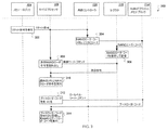
図3はコンピュータ・システム100をリセットするために様々な要素のより実行される動作300を説明するフロー図の一例を示す。動作300は、コンピュータ・システム100の制御、指揮、および監視のうちの少なくともいずれかのもとで実行されてもよい。動作300はまた、コンピュータ・システム100に組み込まれるであろうその他の処理要素と制御要素との少なくともいずれかにより補完されまたは補強されてもよい。単一の要素により実行されると示されていたとしても、動作の一部または全部は、信号に明白に具体化された命令を実行する1以上のプロセッサにより実行されてもよい。処理は、アナログとディジタルとの少なくともいずれかのハードウェアまたは技術を用いて実装されてもよく、単体でまたは1以上のプロセッサが連携して命令を実行してもよい。明確にするために、動作300は、リセット・ロジック104、マイクロプロセッサ108、内部コントローラ120、レジスタ118、およびNANDフラッシュメモリ・ブロック114で生じるとして指し示される。しかしながら、これらの動作や同様の動作を、その他のデバイスや場所により、または、デバイスや場所が異なる構成で実行することができるだろう。
FIG. 3 shows an example of a flow
この例では、コンピュータ・システム100は、3層ブート・プロセスを含む。3層ブート・プロセスでは、マイクロプロセッサ108は最初にNANDフラッシュメモリ・チップ102からNANDローダ・コードを直接的に(すなわち、XIP技術を用いて)実行し、その後にブートローダ・コードをRAM110にロードすることによりブートローラ・コードを実行し、最後にホスト・デバイス106とコンピュータ・システム100とのうちの少なくともいずれかの通常の使用のためにオペレーティング・システムとアプリケーション・プログラムとをロードして起動する。この例では、動作300は、リセット・ロジック104がリセット・コマンドを受信した場合に始まる。(302で、)リセット・ロジック104は、リセット・コマンドに応答して、リセット信号を発生し、マイクロプロセッサ108と内部コントローラ120とにリセット信号を送信する。
In this example,
(304で、)内部コントローラ120は、NANDフラッシュメモリ・ブロック114からデータを読み出すことによって、NANDローダ・コードをレジスタ118にロードする。例えば、リセット信号の受信の際に、所定のページアドレスからレジスタ118にNANDローダ・コードをロードするコマンドを内部コントローラ120が送信するように、内部コントローラ120は所定のページアドレスでプログラムされてもよい。例えば、所定のページアドレスは、NANDフラッシュメモリ・チップ102内の機械スイッチまたは電気回路の配線を用いて製造段階の間にプリセットされていてもよい。代替の実装では、ブートのための所定のデータのページをレジスタ118にロードするコマンドをマイクロプロセッサ108から受信してもよい。(306で、)内部コントローラ120がNANDフラッシュメモリ・ブロック114からデータを読み出した場合に、レジスタ118は、NANDローダ・コードを受信して記憶する。
マイクロプロセッサ108がリセット信号を受信した後に、(308で、)マイクロプロセッサ108は、NANDローダ・コードの次の命令をレジスタ118から読み出すために、単純リード・コマンドを発行する。例として、内部コントローラ120がマイクロプロセッサ108にレディ信号を送信した場合に、マイクロプロセッサ108はレジスタ118から命令の読み出しを始めることができる。別の例として、所定の回数の待ち状態の後に、マイクロプロセッサ108はレジスタ118から命令の読み出しを始めることができる。
After
単純リード・コマンドは、直接実行のためにレジスタ118に記憶されたデータの選択された部分を読み出すことをマイクロプロセッサ108に可能とする点で、従来からあるリード・コマンドと異なる。いくつかの実装では、単純リード・コマンドは、リセット信号を受信した後に生成された従来からある命令フェッチ・コマンドを変換することによって、マイクロプロセッサ108で生成されてもよい。そのほかの実装では単に、リセット信号を受信した後に、マイクロプロセッサ108が一連の単純リード・コマンドを生成するようにプログラムされてもよい。各単純リード・コマンドを、(例えば、一つよりも多いカラムアドレスを含むことによって、)1以上の命令読み出すのに使用することができる。
A simple read command differs from conventional read commands in that it allows the
単純リード・コマンドを用いて、マイクロプロセッサ108は、次の命令を読み出すためにレジスタ118にランダムにアクセスすることができる。例えば、マイクロプロセッサ108は、レジスタ118内のカラムアドレスを指定することによって、レジスタ118から命令を読み出すことができる。これに続いて、マイクロプロセッサ108が次の命令を読み出した場合に、(310で、)マイクロプロセッサ108はローカルRAMに命令をロードせずに、読み出された命令を直接的に実行することができる。いくつかの実装では、リセットの後に最初の命令を読み出すようにアドレスに事前にプログラムされる。例えば、マイクロプロセッサ108は、リセット後に読み出される最初の命令がレジスタ118のアドレス「0」にあるように、事前にプログラムされてもよい。
Using a simple read command, the
マイクロプロセッサ108は、次の命令のアドレスを判定するために様々な方法を用いてもよい。いくつかの実装では、読み出された命令は、次の命令のアドレスに関する情報を含んでもよい。そのほかの実装では、マイクロプロセッサ108は、4のような固定整数分だけ現在の命令のアドレスを増加させることによって、次の命令のアドレスを計算してもよい。いくつかの実装では、マイクロプロセッサ108は、命令がレジスタ118から読み出されることになるアドレスの列でプログラムされてもよい。いくつかの実装では、マイクロプロセッサ108がブート・コードのそのほかの部分を実行する前に、マイクロプロセッサ108は、ステップ308から310を複数回繰り返すことができる。NANDローダ・コードの実行は、ブートローダ・コードのRAM110へのロードとともに、ブートローダ・コードを記憶するためにRAM110を初期化してもよい。
(312で、)マイクロプロセッサ108は、NANDフラッシュメモリ・ブロック114からブートローダ・コードを見つけてロードする命令を実行する。説明および記述の簡略化のために(312での)ブートローダ・コードを見つける動作は(310での)読み出されたNANDローダ命令の実行とは別個の動作として説明されるが、一般的には読み出されたNANDローダ命令の機能および動作の一つはブートローダ・コードを見つけること、または読み出すことであることが理解されよう。従って、312で説明された動作は310での動作と重複してもよく、または310での動作の一部であってもよい。いくつかの実装では、マイクロプロセッサ108は、NANDフラッシュメモリ・ブロック114からブートローダ・コードを見つけて読み出すために、FATまたはHFSのようなファイルシステムを用いることよりもむしろ、機械オペコードを用いることような、ローレベル・アクセス技術を用いる。(314で、)マイクロプロセッサ108は、読み出されたブートローダ・コードをRAM110に記憶し、RAM110からブートローダ・コードを実行する。従来通りのシステムのように、ブートローダ・コードは、通常の動作モードでホスト・デバイス106またはコンピュータ・システム100に配置するために、オペレーティング・システムとアプリケーション・ソフトウェアとのうちの少なくともいずれかをロードして初期化するように動作する。
The
図4はNANDローダ・コードにより実行されるであろうプロセス400のフローチャートの一例を示す。前述したように、NANDローダ・コードはNANDフラッシュメモリ・チップ102内の所定のページに記憶される。いくつかの実装では、内部コントローラ120がリセット信号を検出した場合に、内部コントローラ120はNANDローダ・コードをレジスタ118に自動的にロードする。NANDローダ・コードに含まれる命令を、マイクロプロセッサ108はレジスタ118から直接的に実行することができる。従って、(402で、)内部コントローラ120はNANDローダ・コードをレジスタにロードして、マイクロプロセッサ108はNANDフラッシュメモリ・チップ102から読み出されたNANDローダ・コード内の命令を直接的に実行し始める。
FIG. 4 shows an example of a flowchart of a
NANDローダ・コード内の命令を用いて、(404で、)マイクロプロセッサ108は、RAM110およびマイクロプロセッサ108内のブートのためのその他のハードウェア(例えば、プログラム・カウンタと状態レジスタ)のようなハードウェアを初期化する。その後、(406で、)マイクロプロセッサ108は、NANDフラッシュメモリ内の別のロケーションに記憶されたブートローダ・コードを見つける。いくつかの実装では、NANDローダ・コードのいくつかの命令は、ブートローダ・コードのページアドレスを含む。その他の実装では、NANDローダ・コードは、マイクロプロセッサ108がブートローダ・コードのメモリアドレスを計算することを可能とする命令を含んでもよい。例えば、命令は、ブートローラ・コードのメモリアドレスが現在の命令のアドレスとオフセット値との合計となるオフセット値を含んでもよい。
Using instructions in the NAND loader code, the microprocessor 108 (at 404) causes the hardware such as
次に、(408で、)マイクロプロセッサ108は、ブートローダ・コードをRAM110にリードする。マイクロプロセッサ108は、ローレベル・アクセス技術を用いてブートローダ・コードをRAM110にリードしてもよい。ブートローダ・コードがRAM110に記憶された後に、(410で、)マイクロプロセッサ108は、ブートローダ・コードに実行制御を転送するためにNANDローダ・コード内の命令を実行する。プロセス400は412で終了する。
The
本明細書において説明された発明とほとんどの機能的動作とは、ディジタル電子回路で、または、コンピュータ・ソフトウェア、ファームウェア、もしくはハードウェアで実装されてもよく、本明細書で公開された構造上の手段およびこれらの構造上の均等物、またはこれらの組合せを含む。本発明は、データ処理装置、例えばプログラム可能なプロセッサ、コンピュータ、もしくは複合コンピュータによる実行のための、または、データ処理装置の動作の制御のための、1以上のコンピュータ・プログラム製品、すわなち情報媒体、例えば機械で読み取り可能な記憶デバイスや伝播信号に明白に具現化された1以上のコンピュータ・プログラムとして実装されてもよい。(プログラム、ソフトウェア、ソフトウェア・アプリケーション、またはコードとしても知られる)コンピュータ・プログラムは、コンパイルされた言語またはインタプリタされた言語を含む任意の形式のプログラミング言語で書かれてもよく、スタンドアロン・プログラムまたはモジュール、コンポーネント、サブルーチン、もしくはコンピューティング環境での使用に適したその他のユニットを含む任意の形式で展開されてもよい。コンピュータ・プログラムはファイルに対応する必要はない。プログラムは、他のプログラムやデータを保持するファイルの部分に記憶され、対象のプログラムで専有される単一のファイルに記憶され、または複数の統合されたファイル(例えば、1以上のモジュール、サブプログラム、またはコードの部分)に記憶されてもよい。コンピュータ・プログラムは、一つの場所の、または複数の場所に分散され通信ネットワークで相互接続された、一つのコンピュータまたは複数のコンピュータに、実行のために分配されてもよい。 The invention and most functional operations described herein may be implemented in digital electronic circuitry or in computer software, firmware, or hardware, and on the structural features disclosed herein. Means and structural equivalents thereof, or combinations thereof. The present invention relates to one or more computer program products, i.e. information, for execution by a data processing device, e.g. a programmable processor, computer or complex computer, or for controlling the operation of a data processing device It may be implemented as one or more computer programs tangibly embodied in a medium, such as a machine readable storage device or a propagated signal. A computer program (also known as a program, software, software application, or code) may be written in any form of programming language, including a compiled or interpreted language, and may be a stand-alone program or module , Components, subroutines, or other units suitable for use in a computing environment may be deployed. Computer programs do not need to support files. The program is stored in a part of a file that holds other programs and data, stored in a single file that is exclusively used by the target program, or a plurality of integrated files (eg, one or more modules, subprograms) Or a portion of the code). A computer program may be distributed for execution to one computer or to multiple computers at one location or distributed across multiple locations and interconnected by a communication network.
本発明の方法ステップを含む、本明細書に記載されたプロセスおよびロジックのフローは、入力データを操作して出力を生成することにより本発明の機能を実行するために、1以上のコンピュータ・プログラムを実行する1以上のプログラム可能なプロセッサにより実行されてもよい。プロセスおよびロジックのフローの部分は、特殊目的の論理回路、例えばFPGA(フィールド・プログラマブル・ゲート・アレイ)やASIC(特定用途向け集積回路)により実行されてもよく、本発明の装置は特殊目的の論理回路として実装されてもよい。 The process and logic flow described herein, including the method steps of the present invention, includes one or more computer programs for performing the functions of the present invention by manipulating input data to produce output. May be executed by one or more programmable processors that execute. Portions of the process and logic flow may be performed by special purpose logic circuits such as FPGAs (Field Programmable Gate Arrays) or ASICs (Application Specific Integrated Circuits), and the apparatus of the present invention It may be implemented as a logic circuit.
一例として、コンピュータ・プログラムの実行に適したプロセッサは、汎用目的および特殊目的の両方のマイクロプロセッサと、任意の種類のディジタル・コンピュータの任意の1以上のプロセッサとを含む。一般に、プロセッサは、リードオンリーメモリもしくはランダムアクセスメモリまたはこれらの両方から命令とデータとを受信するだろう。コンピュータの不可欠な要素は、命令の実行のためのプロセッサと命令およびデータを記憶するための1以上のメモリ・デバイスとである。一般に、コンピュータは、1以上の大容量記憶デバイス、例えば磁気ディスク、光磁気ディスク、または光ディスクを含み、または、これらからデータを受信し、これらにデータを送信し、またはこの両方を行う動作が可能なように結合される。コンピュータ・プログラムの命令とデータとの具体化に適した情報媒体は、一例として半導体メモリ・デバイス、例えばEPROM、EEPROM、およびフラッシュメモリ・デバイスと、磁気ディスク、例えば内部ハードディスクまたは取り外し可能なディスクと、光磁気ディスクと、CDROMディスクおよびDVD−ROMディスクとを含む、すべての形式の不揮発性メモリを含む。いくつかの実装では、記載されたプロセスと技術とが、NANDフラッシュメモリまたはその他の個々のメモリ・ロケーションが別個にアドレス指定できない不揮発性メモリに関連する使用に制限されてもよい。プロセッサとメモリとは、特殊目的の論理回路のより補完され、または特主目的の論理回路に組み込まれてもよい。 By way of example, processors suitable for the execution of computer programs include both general purpose and special purpose microprocessors and any one or more processors of any kind of digital computer. Generally, a processor will receive instructions and data from a read-only memory or a random access memory or both. The essential elements of a computer are a processor for execution of instructions and one or more memory devices for storing instructions and data. Generally, a computer includes one or more mass storage devices, such as a magnetic disk, a magneto-optical disk, or an optical disk, or is capable of receiving data from, sending data to, or both Are combined. Information media suitable for the implementation of computer program instructions and data include, by way of example, semiconductor memory devices such as EPROM, EEPROM, and flash memory devices, and magnetic disks such as internal hard disks or removable disks, It includes all types of non-volatile memory, including magneto-optical disks, CDROM disks and DVD-ROM disks. In some implementations, the described processes and techniques may be limited to use in connection with NAND flash memory or other non-volatile memory that cannot be individually addressed by individual memory locations. The processor and the memory may be supplemented by special purpose logic circuits or may be incorporated into special purpose logic circuits.
ユーザとの対話を提供するために、本発明は、ユーザに情報を表示するためのディスプレイ・デバイス、例えばCRT(ブラウン管)またはLCD(液晶ディスプレイ)モニタと、ユーザがコンピュータへの入力を提供できるキーボードおよびポインティング・デバイス例えばマウスまたはトラックボールとを有するコンピュータで実装されてもよい。その上、その他の種類のデバイスが、対話を提供するために用いられてもよい。例えば、ユーザに提供されるフィードバックは、任意の形式の感覚フィードバック、例えば視覚フィードバック、聴覚フィードバック、または触覚フィードバックであってもよい。ユーザからの入力は、音響の、言語の、または触覚の入力を含む、任意の形式で受信されてもよい。 In order to provide user interaction, the present invention provides a display device for displaying information to the user, such as a CRT (CRT) or LCD (Liquid Crystal Display) monitor, and a keyboard that allows the user to provide input to the computer. And a computer having a pointing device such as a mouse or trackball. Moreover, other types of devices may be used to provide interaction. For example, the feedback provided to the user may be any form of sensory feedback, such as visual feedback, audio feedback, or tactile feedback. Input from the user may be received in any form, including acoustic, linguistic, or haptic input.
多くの実装が記載されてきた。しかしながら、様々な変形がなされることが理解されよう。例えば、いくつかの場合では、説明され図面に記載されたのと異なる順番で動作が実行されてもよい。さらに、一般的にバイト単位を基盤としたランダムなデータのアクセスと読み出しとの少なくともいずれかをすることができないその他のメモリのような、NANDフラッシュメモリ以外の不揮発性メモリに関連して技術が使用されてもよい。さらに、フラッシュメモリ・ブロックからレジスタに所定のデータのページをロードすることは、リセット信号の受信以外の1以上の所定の条件に応答して実行されてもよい。従って、その他の実装は添付の請求の範囲内にあるものである。 A number of implementations have been described. However, it will be understood that various modifications may be made. For example, in some cases, operations may be performed in a different order than described and illustrated in the drawings. In addition, the technology is used in conjunction with non-NAND flash memory other than NAND flash memory, such as other memories that are generally unable to access and / or read random data based on byte units. May be. Further, loading a predetermined page of data from the flash memory block to the register may be performed in response to one or more predetermined conditions other than receiving a reset signal. Accordingly, other implementations are within the scope of the appended claims.
Claims (14)
前記デバイスに関連付けられたリセット信号を検出する工程と、
前記不揮発性メモリ集積回路に実装された制御部が、前記リセット信号の検出に応答して、前記不揮発性メモリ集積回路内のメモリ・ロケーションから前記不揮発性メモリ集積回路に実装されたレジスタに所定のデータのページを転送する工程であって、データのページのそれぞれは一体として該不揮発性メモリから読み出され、該データのページは前記デバイスのブートに用いる命令を含む工程と、
前記レジスタに記憶されたデータを直接にリードするコマンドを前記デバイスの別の集積回路に実装されたプロセッサから受信する工程であって、該コマンドは前記不揮発性メモリによって処理可能であり、該レジスタ内の少なくとも一つの命令のロケーションを含んでいる前記データの部分を特定するアドレスを含む工程と、
ランダムアクセスメモリの使用と無関係に前記プロセッサによる実行のために前記レジスタから前記少なくとも一つの命令を読み出す工程と
を備えることを特徴とする方法。 A method for booting a device including a non-volatile memory integrated circuit comprising:
Detecting a reset signal associated with the device;
In response to detection of the reset signal, a control unit mounted on the nonvolatile memory integrated circuit performs a predetermined operation on a register mounted on the nonvolatile memory integrated circuit from a memory location in the nonvolatile memory integrated circuit. Transferring a page of data, each page of data being read as a unit from the non-volatile memory, the page of data including instructions used to boot the device;
Receiving a command for directly reading the data stored in the register from a processor mounted on another integrated circuit of the device, the command being processable by the non-volatile memory; Including an address identifying the portion of the data that includes at least one instruction location of:
Reading the at least one instruction from the register for execution by the processor independent of the use of random access memory.
ページにグループ化された第1の複数のメモリ・ロケーションであって、データのページのそれぞれは第2の複数のメモリ・ロケーションを含み、該第2の複数のメモリ・ロケーションは該第1の複数のメモリ・ロケーションよりも数が少なく、前記メモリ・ロケーション内のデータは各ページを全体として読み出すことによりアクセス可能である第1の複数のメモリ・ロケーションと、
レジスタと、
所定の条件に応答して前記レジスタに所定のデータのページを転送するように構成されるとともに、前記レジスタ内のアドレスのデータを読み出すことによって、所定の受信コマンドに応答するように構成されるコントローラと
を備え、
前記所定の条件は、リセット信号の受信を備えることを特徴とする不揮発性メモリ。 Non-volatile memory,
A first plurality of memory locations grouped into pages, each page of data including a second plurality of memory locations, wherein the second plurality of memory locations is the first plurality of memory locations. A plurality of memory locations, wherein data in said memory locations is accessible by reading each page as a whole; and
Registers,
A controller configured to transfer a page of predetermined data to the register in response to a predetermined condition and configured to respond to a predetermined received command by reading data at an address in the register It equipped with a door,
The non-volatile memory , wherein the predetermined condition comprises receiving a reset signal .
デバイスのための所定の条件を検出する手段と、
前記所定の条件の検出に応答して不揮発性メモリ集積回路内のメモリ・ロケーションから該不揮発性メモリ集積回路に実装されたレジスタに所定のデータのページを転送する該不揮発性メモリ集積回路に実装された制御部のための手段であって、データのページのそれぞれは一体として該不揮発性メモリから読み出され、該データのページは前記デバイスのブートに用いる命令を含む手段と、
前記レジスタに記憶されたデータを直接にリードするコマンドを、別の集積回路に実装された前記デバイスのプロセッサから受信する手段であって、該コマンドは前記不揮発性メモリによって処理可能であり、該レジスタ内の少なくとも一つの命令のロケーションを含んでいる前記データの部分を特定するアドレスを含む手段と、
ランダムアクセスメモリの使用と無関係に前記プロセッサによる実行のために前記レジスタから前記少なくとも一つの命令を読み出す手段と
を備え、
前記所定の条件は、リセット信号の受信を備えることを特徴とするブート・システム。 A boot system,
Means for detecting a predetermined condition for the device;
Implemented in the non-volatile memory integrated circuit for transferring a predetermined page of data from a memory location in the non-volatile memory integrated circuit to a register implemented in the non-volatile memory integrated circuit in response to detection of the predetermined condition Means for the controller, wherein each of the pages of data is read as a unit from the non-volatile memory, the page of data including instructions used to boot the device;
Means for receiving a command for directly reading data stored in said register from a processor of said device mounted on another integrated circuit, said command being processable by said non-volatile memory; Means including an address identifying the portion of the data that includes the location of at least one instruction in
Means for reading the at least one instruction from the register for execution by the processor independently of the use of random access memory ;
The boot system , wherein the predetermined condition comprises receiving a reset signal .
Applications Claiming Priority (3)
| Application Number | Priority Date | Filing Date | Title |
|---|---|---|---|
| US11/400,854 | 2006-04-10 | ||
| US11/400,854 US7849302B2 (en) | 2006-04-10 | 2006-04-10 | Direct boot arrangement using a NAND flash memory |
| PCT/US2007/066333 WO2007121181A1 (en) | 2006-04-10 | 2007-04-10 | Direct boot arrangement using a nand flash memory |
Publications (3)
| Publication Number | Publication Date |
|---|---|
| JP2009533770A JP2009533770A (en) | 2009-09-17 |
| JP2009533770A5 JP2009533770A5 (en) | 2010-01-14 |
| JP5284946B2 true JP5284946B2 (en) | 2013-09-11 |
Family
ID=38510933
Family Applications (1)
| Application Number | Title | Priority Date | Filing Date |
|---|---|---|---|
| JP2009505574A Active JP5284946B2 (en) | 2006-04-10 | 2007-04-10 | Direct boot configuration using NAND flash memory |
Country Status (6)
| Country | Link |
|---|---|
| US (4) | US7849302B2 (en) |
| EP (2) | EP3299958B1 (en) |
| JP (1) | JP5284946B2 (en) |
| KR (1) | KR101035473B1 (en) |
| CN (1) | CN101421701B (en) |
| WO (1) | WO2007121181A1 (en) |
Families Citing this family (47)
| Publication number | Priority date | Publication date | Assignee | Title |
|---|---|---|---|---|
| US7596709B2 (en) * | 2000-12-30 | 2009-09-29 | Intel Corporation | CPU power management based on utilization with lowest performance mode at the mid-utilization range |
| KR100804647B1 (en) * | 2005-11-15 | 2008-02-20 | 삼성전자주식회사 | Method and apparatus for booting system using serial flash memory device having parallel flash interface |
| KR101030385B1 (en) | 2006-02-13 | 2011-04-20 | 삼성전자주식회사 | Booting apparatus and method for system with only internal memory |
| US7822958B1 (en) * | 2006-03-10 | 2010-10-26 | Altera Corporation | Booting mechanism for FPGA-based embedded system |
| US7849302B2 (en) | 2006-04-10 | 2010-12-07 | Apple Inc. | Direct boot arrangement using a NAND flash memory |
| KR20080011627A (en) * | 2006-07-31 | 2008-02-05 | 윤동구 | Computer system and booting method of the same |
| TWI327290B (en) * | 2006-10-03 | 2010-07-11 | Magic Pixel Inc | Electronic system with nand flash memory storing boot code and a highly reliable boot up method |
| KR101395778B1 (en) * | 2007-03-14 | 2014-05-19 | 삼성전자주식회사 | Memory card and memory system including the same and operating method thereof |
| US8028155B1 (en) * | 2007-06-06 | 2011-09-27 | American Megatrends, Inc. | Initiating an operating system boot from firmware |
| KR101211503B1 (en) * | 2007-10-02 | 2012-12-12 | 삼성전자주식회사 | Booting system, image forming apparatus having the system and method thereof |
| US7886141B2 (en) * | 2007-10-27 | 2011-02-08 | Asix Electronics Corporation | Method and systems for advanced reprogrammable boot codes and in-application programming of embedded microprocessor systems |
| TWI383319B (en) * | 2008-11-26 | 2013-01-21 | Via Tech Inc | Computer system and booting method of same |
| JP2010134741A (en) * | 2008-12-05 | 2010-06-17 | Internatl Business Mach Corp <Ibm> | Method and system for executing program |
| JP2010140266A (en) * | 2008-12-11 | 2010-06-24 | Toshiba Corp | Electronic device system and electronic device |
| KR101542878B1 (en) * | 2009-02-13 | 2015-08-07 | 삼성전자주식회사 | Nonvolatile memory device having a buffer ram and boot code management method thereof |
| JPWO2011001486A1 (en) * | 2009-06-30 | 2012-12-10 | パナソニック株式会社 | Data processing method, semiconductor integrated circuit |
| US10360143B2 (en) | 2010-07-01 | 2019-07-23 | Qualcomm Incorporated | Parallel use of integrated non-volatile memory and main volatile memory within a mobile device |
| TWI456577B (en) * | 2010-08-10 | 2014-10-11 | Hon Hai Prec Ind Co Ltd | Nand flash startup device and using method of the same |
| US8799555B2 (en) * | 2011-04-14 | 2014-08-05 | Apple Inc. | Boot data storage schemes for electronic devices |
| EP2557497A1 (en) * | 2011-08-08 | 2013-02-13 | Advanced Digital Broadcast S.A. | Method for improving booting of a computing device |
| CN108549609B (en) * | 2011-09-30 | 2022-06-21 | 英特尔公司 | Non-volatile random access memory (NVRAM) as a replacement for conventional mass storage devices |
| US9348783B2 (en) | 2012-04-19 | 2016-05-24 | Lockheed Martin Corporation | Apparatus and method emulating a parallel interface to effect parallel data transfer from serial flash memory |
| US8990549B2 (en) | 2012-07-12 | 2015-03-24 | Freescale Semiconductor, Inc. | Method and system for booting electronic device from NAND flash memory |
| JP5971022B2 (en) * | 2012-08-15 | 2016-08-17 | 富士ゼロックス株式会社 | Image forming apparatus |
| US8873747B2 (en) | 2012-09-25 | 2014-10-28 | Apple Inc. | Key management using security enclave processor |
| US9047471B2 (en) * | 2012-09-25 | 2015-06-02 | Apple Inc. | Security enclave processor boot control |
| JP5619198B2 (en) * | 2013-02-04 | 2014-11-05 | 株式会社フィックスターズ | Information processing apparatus, information processing method, and program |
| KR20140100008A (en) | 2013-02-05 | 2014-08-14 | 삼성전자주식회사 | Method of operating a volatile memory device and method of testing a volatile memory device |
| US9471357B2 (en) * | 2013-09-13 | 2016-10-18 | American Megatrends, Inc. | Monitoring virtual machine interface and local graphical user interface on a thin client and alternating therebetween |
| TWI540508B (en) * | 2013-11-01 | 2016-07-01 | 慧榮科技股份有限公司 | Firmware loading system and firmware loading method |
| US9436480B1 (en) * | 2013-11-08 | 2016-09-06 | Western Digital Technologies, Inc. | Firmware RAM usage without overlays |
| US10331457B2 (en) * | 2014-01-22 | 2019-06-25 | Hewlett-Packard Development Company, L.P. | Byte-addressable non-volatile read-write main memory partitioned into regions including metadata region |
| US9547778B1 (en) | 2014-09-26 | 2017-01-17 | Apple Inc. | Secure public key acceleration |
| US9479265B2 (en) * | 2015-02-16 | 2016-10-25 | American Megatrends, Inc. | System and method for high speed and efficient virtual desktop insfrastructure using photonics |
| TWI573033B (en) * | 2016-01-14 | 2017-03-01 | 群聯電子股份有限公司 | Data searching method, memory storage device and memory control circuit unit |
| CN106991055B (en) * | 2016-01-21 | 2021-01-12 | 群联电子股份有限公司 | Data search method, memory storage device and memory control circuit unit |
| CN106302261B (en) * | 2016-08-02 | 2019-09-17 | 青岛海信电器股份有限公司 | A kind of method and apparatus of control command forwarding |
| KR102387461B1 (en) | 2017-07-24 | 2022-04-15 | 삼성전자주식회사 | Storage device, storage system and operating method thereof |
| TWI645296B (en) * | 2017-10-17 | 2018-12-21 | 慧榮科技股份有限公司 | Data storage device and control method for non-volatile memory |
| CN108920194A (en) * | 2018-06-08 | 2018-11-30 | 山东超越数控电子股份有限公司 | A kind of method of Domestic Platform BIOS starting EXT file system |
| TWI677879B (en) * | 2018-09-03 | 2019-11-21 | 慧榮科技股份有限公司 | A data storage device and a data processing method |
| US10852949B2 (en) * | 2019-04-15 | 2020-12-01 | Micron Technology, Inc. | Predictive data pre-fetching in a data storage device |
| US11237838B2 (en) * | 2020-01-02 | 2022-02-01 | Western Digital Technologies, Inc. | Storage system and method for enabling a direct accessible boot block in a memory die |
| CN115151895A (en) * | 2020-04-01 | 2022-10-04 | 松下知识产权经营株式会社 | Storage system |
| US11640308B2 (en) | 2021-02-19 | 2023-05-02 | Macronix International Co., Ltd. | Serial NAND flash with XiP capability |
| CN114253615B (en) * | 2021-12-16 | 2023-08-11 | 安天科技集团股份有限公司 | Method and device for setting bootstrap program, electronic equipment and storage medium |
| WO2024044876A1 (en) * | 2022-08-29 | 2024-03-07 | Micron Technology, Inc. | Receiving executable instructions from volatile memory |
Family Cites Families (34)
| Publication number | Priority date | Publication date | Assignee | Title |
|---|---|---|---|---|
| EP0618535B1 (en) * | 1989-04-13 | 1999-08-25 | SanDisk Corporation | EEPROM card with defective cell substitution and cache memory |
| US5663901A (en) * | 1991-04-11 | 1997-09-02 | Sandisk Corporation | Computer memory cards using flash EEPROM integrated circuit chips and memory-controller systems |
| JPH05282882A (en) * | 1991-12-19 | 1993-10-29 | Toshiba Corp | Nonvolatile semiconductor memory |
| US7137011B1 (en) * | 1993-09-01 | 2006-11-14 | Sandisk Corporation | Removable mother/daughter peripheral card |
| US5696917A (en) | 1994-06-03 | 1997-12-09 | Intel Corporation | Method and apparatus for performing burst read operations in an asynchronous nonvolatile memory |
| US5748551A (en) | 1995-12-29 | 1998-05-05 | Micron Technology, Inc. | Memory device with multiple internal banks and staggered command execution |
| US5892777A (en) | 1997-05-05 | 1999-04-06 | Motorola, Inc. | Apparatus and method for observing the mode of a memory device |
| KR100274602B1 (en) | 1997-11-20 | 2000-12-15 | 윤종용 | Synchronous memory device |
| JP4252139B2 (en) * | 1998-12-16 | 2009-04-08 | 株式会社日立製作所 | Storage system |
| US6601167B1 (en) * | 2000-01-14 | 2003-07-29 | Advanced Micro Devices, Inc. | Computer system initialization with boot program stored in sequential access memory, controlled by a boot loader to control and execute the boot program |
| US6426893B1 (en) * | 2000-02-17 | 2002-07-30 | Sandisk Corporation | Flash eeprom system with simultaneous multiple data sector programming and storage of physical block characteristics in other designated blocks |
| US6314049B1 (en) | 2000-03-30 | 2001-11-06 | Micron Technology, Inc. | Elimination of precharge operation in synchronous flash memory |
| KR100508041B1 (en) * | 2000-03-30 | 2005-08-17 | 마이크론 테크놀로지, 인크. | Interface command architecture for synchronous flash memory |
| US6763424B2 (en) * | 2001-01-19 | 2004-07-13 | Sandisk Corporation | Partial block data programming and reading operations in a non-volatile memory |
| JP4017177B2 (en) * | 2001-02-28 | 2007-12-05 | スパンション エルエルシー | Memory device |
| US6871257B2 (en) * | 2002-02-22 | 2005-03-22 | Sandisk Corporation | Pipelined parallel programming operation in a non-volatile memory system |
| US7234052B2 (en) * | 2002-03-08 | 2007-06-19 | Samsung Electronics Co., Ltd | System boot using NAND flash memory and method thereof |
| US20030206442A1 (en) * | 2002-05-02 | 2003-11-06 | Jerry Tang | Flash memory bridiging device, method and application system |
| US6721820B2 (en) * | 2002-05-15 | 2004-04-13 | M-Systems Flash Disk Pioneers Ltd. | Method for improving performance of a flash-based storage system using specialized flash controllers |
| KR100463201B1 (en) * | 2002-05-28 | 2004-12-23 | 삼성전자주식회사 | Power detecting circuit, a flash memory device using the same, a method of generating power-on read signal of the flash memory device and a stable power-on reading method of the flash memory device |
| KR100448905B1 (en) * | 2002-07-29 | 2004-09-16 | 삼성전자주식회사 | Computer system with nand flash memory for booting and storagement |
| US7082525B2 (en) * | 2002-10-02 | 2006-07-25 | Sandisk Corporation | Booting from non-linear memory |
| KR100493884B1 (en) | 2003-01-09 | 2005-06-10 | 삼성전자주식회사 | Control apparatus and method for xip(execution in place) in serial flash memory and flash memory chip using the same |
| EP1609048A4 (en) * | 2003-03-27 | 2009-01-14 | Milsys Ltd | Data storage device with full access by all users |
| JP4314057B2 (en) * | 2003-04-18 | 2009-08-12 | サンディスク コーポレイション | Nonvolatile semiconductor memory device and electronic device |
| US7240219B2 (en) * | 2003-05-25 | 2007-07-03 | Sandisk Il Ltd. | Method and system for maintaining backup of portable storage devices |
| US7237074B2 (en) * | 2003-06-13 | 2007-06-26 | Sandisk Corporation | Tracking cells for a memory system |
| US7257703B2 (en) * | 2003-11-18 | 2007-08-14 | Toshiba America Electronic Components, Inc. | Bootable NAND flash memory architecture |
| JP4745613B2 (en) * | 2004-01-20 | 2011-08-10 | キヤノン株式会社 | Information processing apparatus and information processing method |
| WO2005076137A1 (en) | 2004-02-05 | 2005-08-18 | Research In Motion Limited | Memory controller interface |
| US20050204091A1 (en) * | 2004-03-11 | 2005-09-15 | Kilbuck Kevin M. | Non-volatile memory with synchronous DRAM interface |
| KR100607992B1 (en) * | 2004-07-09 | 2006-08-02 | 삼성전자주식회사 | Method and system for booting system by monitoring operating status of NAND flash memory |
| WO2006026645A2 (en) * | 2004-08-30 | 2006-03-09 | Silicon Storage Technology, Inc. | Systems and methods for providing nonvolatile memory management in wireless phones |
| US7849302B2 (en) * | 2006-04-10 | 2010-12-07 | Apple Inc. | Direct boot arrangement using a NAND flash memory |
-
2006
- 2006-04-10 US US11/400,854 patent/US7849302B2/en active Active
-
2007
- 2007-04-10 EP EP17200357.6A patent/EP3299958B1/en active Active
- 2007-04-10 EP EP07760402.3A patent/EP2005295B1/en active Active
- 2007-04-10 JP JP2009505574A patent/JP5284946B2/en active Active
- 2007-04-10 CN CN2007800129114A patent/CN101421701B/en active Active
- 2007-04-10 WO PCT/US2007/066333 patent/WO2007121181A1/en active Application Filing
- 2007-04-10 KR KR1020087027317A patent/KR101035473B1/en active IP Right Grant
-
2010
- 2010-12-06 US US12/961,449 patent/US8533448B2/en active Active
-
2013
- 2013-09-10 US US14/022,576 patent/US8832423B2/en active Active
-
2014
- 2014-08-01 US US14/449,365 patent/US9122493B2/en active Active
Also Published As
| Publication number | Publication date |
|---|---|
| WO2007121181A1 (en) | 2007-10-25 |
| US20070239977A1 (en) | 2007-10-11 |
| US20140013097A1 (en) | 2014-01-09 |
| US8533448B2 (en) | 2013-09-10 |
| KR20090024117A (en) | 2009-03-06 |
| CN101421701B (en) | 2013-01-02 |
| EP3299958B1 (en) | 2024-03-27 |
| US20110078432A1 (en) | 2011-03-31 |
| EP2005295A1 (en) | 2008-12-24 |
| EP2005295B1 (en) | 2017-11-08 |
| US9122493B2 (en) | 2015-09-01 |
| US8832423B2 (en) | 2014-09-09 |
| CN101421701A (en) | 2009-04-29 |
| JP2009533770A (en) | 2009-09-17 |
| US7849302B2 (en) | 2010-12-07 |
| US20140344564A1 (en) | 2014-11-20 |
| EP3299958A1 (en) | 2018-03-28 |
| KR101035473B1 (en) | 2011-05-18 |
Similar Documents
| Publication | Publication Date | Title |
|---|---|---|
| JP5284946B2 (en) | Direct boot configuration using NAND flash memory | |
| JP5234473B2 (en) | Turboboot system and method | |
| EP1343082B1 (en) | System boot using nand flash memory and method thereof | |
| KR20110084403A (en) | Preloading applications onto memory at least partially during boot up | |
| TW200830097A (en) | Method and apparatus for saving power for a computing system by providing instant-on resuming from a hibernation state | |
| US20100036973A1 (en) | Storage device for mounting to a host | |
| CN101650660A (en) | Booting a computer system from central storage | |
| US8782319B2 (en) | Expandable hybrid storage device and computer system and control method | |
| JP2006079628A (en) | System and method of storing user data in partition file or using partition file containing user data | |
| US20030182546A1 (en) | Information device, storage medium, and system activation method | |
| US20120060023A1 (en) | Methods for booting an operating system using non-volatile memory | |
| US20110113227A1 (en) | Electronic equipment and boot method, storage medium thereof | |
| KR20030028728A (en) | Low power digital audio decoding/playing system for computing devices | |
| US7849300B2 (en) | Method for changing booting sources of a computer system and a related backup/restore method thereof | |
| US8291206B2 (en) | Method for booting computer system | |
| US20060265437A1 (en) | Contiguous boot and resume start-up files | |
| TWI559227B (en) | Computer system having two built-in operating devices that can be dynamically powered on or powered off | |
| US20060168440A1 (en) | OS selection methods and computer systems utilizing the same | |
| KR101120956B1 (en) | Portable multi-platform booting systems and architectures | |
| US20150317181A1 (en) | Operating system switching method | |
| CN102063314B (en) | Starting method for accelerating initialization of window system | |
| EP1914628A1 (en) | Method for changing booting sources of computer system and related backup/restore method thereof | |
| WO2009017575A2 (en) | Electronic device data access system and method | |
| JP2009151707A (en) | Information processor and operating system determination method | |
| JP2004185316A (en) | Storage device assisting execution of computer program in half-activated or activated state |
Legal Events
| Date | Code | Title | Description |
|---|---|---|---|
| A521 | Request for written amendment filed |
Free format text: JAPANESE INTERMEDIATE CODE: A523 Effective date: 20091119 |
|
| A621 | Written request for application examination |
Free format text: JAPANESE INTERMEDIATE CODE: A621 Effective date: 20091119 |
|
| A977 | Report on retrieval |
Free format text: JAPANESE INTERMEDIATE CODE: A971007 Effective date: 20120216 |
|
| A131 | Notification of reasons for refusal |
Free format text: JAPANESE INTERMEDIATE CODE: A131 Effective date: 20120220 |
|
| A02 | Decision of refusal |
Free format text: JAPANESE INTERMEDIATE CODE: A02 Effective date: 20120803 |
|
| A521 | Request for written amendment filed |
Free format text: JAPANESE INTERMEDIATE CODE: A523 Effective date: 20121203 |
|
| A911 | Transfer to examiner for re-examination before appeal (zenchi) |
Free format text: JAPANESE INTERMEDIATE CODE: A911 Effective date: 20121210 |
|
| A131 | Notification of reasons for refusal |
Free format text: JAPANESE INTERMEDIATE CODE: A131 Effective date: 20130107 |
|
| A601 | Written request for extension of time |
Free format text: JAPANESE INTERMEDIATE CODE: A601 Effective date: 20130408 |
|
| A521 | Request for written amendment filed |
Free format text: JAPANESE INTERMEDIATE CODE: A523 Effective date: 20130411 |
|
| A602 | Written permission of extension of time |
Free format text: JAPANESE INTERMEDIATE CODE: A602 Effective date: 20130415 |
|
| TRDD | Decision of grant or rejection written | ||
| A01 | Written decision to grant a patent or to grant a registration (utility model) |
Free format text: JAPANESE INTERMEDIATE CODE: A01 Effective date: 20130507 |
|
| A61 | First payment of annual fees (during grant procedure) |
Free format text: JAPANESE INTERMEDIATE CODE: A61 Effective date: 20130530 |
|
| R150 | Certificate of patent or registration of utility model |
Ref document number: 5284946 Country of ref document: JP Free format text: JAPANESE INTERMEDIATE CODE: R150 |
|
| R250 | Receipt of annual fees |
Free format text: JAPANESE INTERMEDIATE CODE: R250 |
|
| R250 | Receipt of annual fees |
Free format text: JAPANESE INTERMEDIATE CODE: R250 |
|
| R250 | Receipt of annual fees |
Free format text: JAPANESE INTERMEDIATE CODE: R250 |
|
| R250 | Receipt of annual fees |
Free format text: JAPANESE INTERMEDIATE CODE: R250 |
|
| R250 | Receipt of annual fees |
Free format text: JAPANESE INTERMEDIATE CODE: R250 |
|
| R250 | Receipt of annual fees |
Free format text: JAPANESE INTERMEDIATE CODE: R250 |
|
| R250 | Receipt of annual fees |
Free format text: JAPANESE INTERMEDIATE CODE: R250 |
|
| R250 | Receipt of annual fees |
Free format text: JAPANESE INTERMEDIATE CODE: R250 |