US11237838B2 - Storage system and method for enabling a direct accessible boot block in a memory die - Google Patents
Storage system and method for enabling a direct accessible boot block in a memory die Download PDFInfo
- Publication number
- US11237838B2 US11237838B2 US16/732,649 US202016732649A US11237838B2 US 11237838 B2 US11237838 B2 US 11237838B2 US 202016732649 A US202016732649 A US 202016732649A US 11237838 B2 US11237838 B2 US 11237838B2
- Authority
- US
- United States
- Prior art keywords
- code
- storage system
- memory
- nand memory
- initialization
- Prior art date
- Legal status (The legal status is an assumption and is not a legal conclusion. Google has not performed a legal analysis and makes no representation as to the accuracy of the status listed.)
- Active, expires
Links
- 230000015654 memory Effects 0.000 title claims abstract description 216
- 238000000034 method Methods 0.000 title claims abstract description 19
- 230000004044 response Effects 0.000 claims abstract description 16
- 230000006870 function Effects 0.000 claims description 16
- 238000004891 communication Methods 0.000 claims description 5
- 239000000758 substrate Substances 0.000 description 17
- 238000010586 diagram Methods 0.000 description 16
- 239000004065 semiconductor Substances 0.000 description 9
- 238000003491 array Methods 0.000 description 6
- 238000011161 development Methods 0.000 description 4
- 238000012545 processing Methods 0.000 description 4
- 238000012937 correction Methods 0.000 description 3
- 238000005516 engineering process Methods 0.000 description 3
- 230000002093 peripheral effect Effects 0.000 description 3
- 102100031102 C-C motif chemokine 4 Human genes 0.000 description 2
- 101100054773 Caenorhabditis elegans act-2 gene Proteins 0.000 description 2
- 101100000858 Caenorhabditis elegans act-3 gene Proteins 0.000 description 2
- HEFNNWSXXWATRW-UHFFFAOYSA-N Ibuprofen Chemical compound CC(C)CC1=CC=C(C(C)C(O)=O)C=C1 HEFNNWSXXWATRW-UHFFFAOYSA-N 0.000 description 2
- 239000000872 buffer Substances 0.000 description 2
- 230000008859 change Effects 0.000 description 2
- 239000007795 chemical reaction product Substances 0.000 description 2
- 239000000835 fiber Substances 0.000 description 2
- 238000011084 recovery Methods 0.000 description 2
- 229910052710 silicon Inorganic materials 0.000 description 2
- 239000010703 silicon Substances 0.000 description 2
- 238000012546 transfer Methods 0.000 description 2
- 238000013519 translation Methods 0.000 description 2
- 101100161935 Caenorhabditis elegans act-4 gene Proteins 0.000 description 1
- 238000012356 Product development Methods 0.000 description 1
- 239000011370 conductive nanoparticle Substances 0.000 description 1
- 238000013461 design Methods 0.000 description 1
- 239000003989 dielectric material Substances 0.000 description 1
- 230000009977 dual effect Effects 0.000 description 1
- 238000007667 floating Methods 0.000 description 1
- 230000009191 jumping Effects 0.000 description 1
- 238000012005 ligant binding assay Methods 0.000 description 1
- 238000004519 manufacturing process Methods 0.000 description 1
- 230000005055 memory storage Effects 0.000 description 1
- 239000012782 phase change material Substances 0.000 description 1
- 230000008569 process Effects 0.000 description 1
- 239000000047 product Substances 0.000 description 1
- 239000007787 solid Substances 0.000 description 1
- 230000003068 static effect Effects 0.000 description 1
Images


Classifications
-
- G—PHYSICS
- G06—COMPUTING; CALCULATING OR COUNTING
- G06F—ELECTRIC DIGITAL DATA PROCESSING
- G06F9/00—Arrangements for program control, e.g. control units
- G06F9/06—Arrangements for program control, e.g. control units using stored programs, i.e. using an internal store of processing equipment to receive or retain programs
- G06F9/44—Arrangements for executing specific programs
- G06F9/4401—Bootstrapping
- G06F9/4406—Loading of operating system
-
- G—PHYSICS
- G06—COMPUTING; CALCULATING OR COUNTING
- G06F—ELECTRIC DIGITAL DATA PROCESSING
- G06F11/00—Error detection; Error correction; Monitoring
- G06F11/07—Responding to the occurrence of a fault, e.g. fault tolerance
- G06F11/0703—Error or fault processing not based on redundancy, i.e. by taking additional measures to deal with the error or fault not making use of redundancy in operation, in hardware, or in data representation
- G06F11/0706—Error or fault processing not based on redundancy, i.e. by taking additional measures to deal with the error or fault not making use of redundancy in operation, in hardware, or in data representation the processing taking place on a specific hardware platform or in a specific software environment
- G06F11/073—Error or fault processing not based on redundancy, i.e. by taking additional measures to deal with the error or fault not making use of redundancy in operation, in hardware, or in data representation the processing taking place on a specific hardware platform or in a specific software environment in a memory management context, e.g. virtual memory or cache management
-
- G—PHYSICS
- G06—COMPUTING; CALCULATING OR COUNTING
- G06F—ELECTRIC DIGITAL DATA PROCESSING
- G06F11/00—Error detection; Error correction; Monitoring
- G06F11/07—Responding to the occurrence of a fault, e.g. fault tolerance
- G06F11/0703—Error or fault processing not based on redundancy, i.e. by taking additional measures to deal with the error or fault not making use of redundancy in operation, in hardware, or in data representation
- G06F11/0751—Error or fault detection not based on redundancy
-
- G—PHYSICS
- G06—COMPUTING; CALCULATING OR COUNTING
- G06F—ELECTRIC DIGITAL DATA PROCESSING
- G06F11/00—Error detection; Error correction; Monitoring
- G06F11/07—Responding to the occurrence of a fault, e.g. fault tolerance
- G06F11/14—Error detection or correction of the data by redundancy in operation
- G06F11/1402—Saving, restoring, recovering or retrying
- G06F11/1415—Saving, restoring, recovering or retrying at system level
- G06F11/1417—Boot up procedures
-
- G—PHYSICS
- G06—COMPUTING; CALCULATING OR COUNTING
- G06F—ELECTRIC DIGITAL DATA PROCESSING
- G06F3/00—Input arrangements for transferring data to be processed into a form capable of being handled by the computer; Output arrangements for transferring data from processing unit to output unit, e.g. interface arrangements
- G06F3/06—Digital input from, or digital output to, record carriers, e.g. RAID, emulated record carriers or networked record carriers
- G06F3/0601—Interfaces specially adapted for storage systems
- G06F3/0602—Interfaces specially adapted for storage systems specifically adapted to achieve a particular effect
- G06F3/0614—Improving the reliability of storage systems
- G06F3/0617—Improving the reliability of storage systems in relation to availability
-
- G—PHYSICS
- G06—COMPUTING; CALCULATING OR COUNTING
- G06F—ELECTRIC DIGITAL DATA PROCESSING
- G06F3/00—Input arrangements for transferring data to be processed into a form capable of being handled by the computer; Output arrangements for transferring data from processing unit to output unit, e.g. interface arrangements
- G06F3/06—Digital input from, or digital output to, record carriers, e.g. RAID, emulated record carriers or networked record carriers
- G06F3/0601—Interfaces specially adapted for storage systems
- G06F3/0628—Interfaces specially adapted for storage systems making use of a particular technique
- G06F3/0655—Vertical data movement, i.e. input-output transfer; data movement between one or more hosts and one or more storage devices
- G06F3/0659—Command handling arrangements, e.g. command buffers, queues, command scheduling
-
- G—PHYSICS
- G06—COMPUTING; CALCULATING OR COUNTING
- G06F—ELECTRIC DIGITAL DATA PROCESSING
- G06F3/00—Input arrangements for transferring data to be processed into a form capable of being handled by the computer; Output arrangements for transferring data from processing unit to output unit, e.g. interface arrangements
- G06F3/06—Digital input from, or digital output to, record carriers, e.g. RAID, emulated record carriers or networked record carriers
- G06F3/0601—Interfaces specially adapted for storage systems
- G06F3/0668—Interfaces specially adapted for storage systems adopting a particular infrastructure
- G06F3/0671—In-line storage system
- G06F3/0673—Single storage device
- G06F3/068—Hybrid storage device
-
- G—PHYSICS
- G06—COMPUTING; CALCULATING OR COUNTING
- G06F—ELECTRIC DIGITAL DATA PROCESSING
- G06F2201/00—Indexing scheme relating to error detection, to error correction, and to monitoring
- G06F2201/805—Real-time
Definitions
- ROM read-only memory
- a central processing unit (CPU) in the storage system can fetch instructions (code) from Address 0 in the ROM, and execution of the instructions can take place in the ROM.
- the executed instructions cause the CPU to scan for boot blocks in non-volatile memory (e.g., NAND) in the storage system. If the boot blocks are not present, the CPU waits in an idle loop. If the boot blocks are found, the CPU copies bootloader (BLR) code from the NAND to random access memory (RAM). The CPU then starts execution of BLR code in the RAM, which in turn downloads Flashware code to enable operation of other functions of the storage system.
- BLR bootloader
- FIG. 1A is a block diagram of a non-volatile storage system of an embodiment.
- FIG. 1B is a block diagram illustrating a storage module of an embodiment.
- FIG. 1C is a block diagram illustrating a hierarchical storage system of an embodiment.
- FIG. 2A is a block diagram illustrating components of the controller of the non-volatile storage system illustrated in FIG. 1A according to an embodiment.
- FIG. 2B is a block diagram illustrating components of the non-volatile memory storage system illustrated in FIG. 1A according to an embodiment.
- FIG. 3 is a block diagram illustrating a typical boot flow.
- FIG. 4 is a block diagram illustrating a boot flow of an embodiment.
- FIG. 5 is a block diagram illustrating a boot flow of an embodiment.
- FIG. 6 is a flow chart of a method of an embodiment for booting from a memory die.
- a storage system comprising a NAND memory, a volatile memory, a processor, and a NAND controller.
- the NAND controller is configured to perform the following in response to receiving a command from the processor at power-up: read bootloader code from the NAND memory; and execute the bootloader code, wherein execution of the bootloader code causes initialization code to be read from the NAND memory and stored in the volatile memory.
- the processor is configured to read secondary bootloader code from the NAND memory in response to an error.
- the error comprises a problem with the execution of the bootloader code that prevents the initialization code from being read from the NAND memory.
- the error comprises an error in the initialization code.
- the bootloader code in executed in place in the NAND memory.
- an address of the bootloader code in the NAND memory is mapped in the processor.
- the NAND memory comprises a three-dimensional memory.
- the storage system is configured to be integrated in a host.
- the storage system is configured to be removably connected with a host.
- a method for booting a storage system is presented that is performed in a storage system comprising NAND memory.
- the method comprises: attempting to load first stage bootloader code from the NAND memory at start-up of the storage system; in response to the attempt to load the first stage bootloader code from the NAND memory being successful, executing the first stage bootloader code; using the executed first stage bootloader code to load initialization code from the NAND memory and executing the initialization code; and using the executed initialization code to load a bootloader code from the NAND memory and executing the bootloader code to boot the storage system.
- the method further comprises in response to the attempt to execute the first stage bootloader code from the NAND memory being unsuccessful, attempting to read a secondary copy of the first stage bootloader code from the NAND memory.
- the method further comprises determining whether the initialization code is required.
- the method further comprises determining whether boot blocks are present in the NAND memory; and in response to determining that boot blocks are not present in the NAND memory, downloading a tool to create a boot block.
- the method further comprises performing a watchdog function in response to an error.
- a storage system comprising a NAND memory configured to store bootloader code and initialization code; means for reading the bootloader code from the NAND memory; and means for executing the bootloader code, wherein execution of the bootloader code causes the initialization code to be read from the NAND memory to boot the storage system.
- the storage system further comprises means for reading secondary bootloader code from the NAND memory in response to an error.
- the error comprises a problem with the execution of the bootloader code that prevents the initialization code from being read from the NAND memory.
- the error comprises an error in the initialization code.
- the NAND memory comprises a three-dimensional memory.
- the storage system is configured to be integrated in a host.
- FIG. 1A is a block diagram illustrating a non-volatile storage system 100 (sometimes referred to herein as a storage device or just device) according to an embodiment of the subject matter described herein.
- non-volatile storage system 100 includes a controller 102 and non-volatile memory that may be made up of one or more non-volatile memory die 104 .
- the term die refers to the collection of non-volatile memory cells, and associated circuitry for managing the physical operation of those non-volatile memory cells, that are formed on a single semiconductor substrate.
- Controller 102 interfaces with a host system and transmits command sequences for read, program, and erase operations to non-volatile memory die 104 .
- the controller 102 (which may be a non-volatile memory controller (e.g., a flash, resistive random-access memory (ReRAM), phase-change memory (PCM), or magnetoresistive random-access memory (MRAM) controller)) can take the form of processing circuitry, a microprocessor or processor, and a computer-readable medium that stores computer-readable program code (e.g., firmware) executable by the (micro)processor, logic gates, switches, an application specific integrated circuit (ASIC), a programmable logic controller, and an embedded microcontroller, for example.
- the controller 102 can be configured with hardware and/or firmware to perform the various functions described below and shown in the flow diagrams.
- the components shown as being internal to the controller can also be stored external to the controller, and other components can be used. Additionally, the phrase “operatively in communication with” could mean directly in communication with or indirectly (wired or wireless) in communication with through one or more components, which may or may not be shown or described herein.
- a non-volatile memory controller is a device that manages data stored on non-volatile memory and communicates with a host, such as a computer or electronic device.
- a non-volatile memory controller can have various functionality in addition to the specific functionality described herein.
- the non-volatile memory controller can format the non-volatile memory to ensure the memory is operating properly, map out bad non-volatile memory cells, and allocate spare cells to be substituted for future failed cells. Some part of the spare cells can be used to hold firmware to operate the non-volatile memory controller and implement other features.
- a host needs to read data from or write data to the non-volatile memory, it can communicate with the non-volatile memory controller.
- the non-volatile memory controller can convert the logical address received from the host to a physical address in the non-volatile memory. (Alternatively, the host can provide the physical address.)
- the non-volatile memory controller can also perform various memory management functions, such as, but not limited to, wear leveling (distributing writes to avoid wearing out specific blocks of memory that would otherwise be repeatedly written to) and garbage collection (after a block is full, moving only the valid pages of data to a new block, so the full block can be erased and reused).
- wear leveling distributing writes to avoid wearing out specific blocks of memory that would otherwise be repeatedly written to
- garbage collection after a block is full, moving only the valid pages of data to a new block, so the full block can be erased and reused.
- the structure for the “means” recited in the claims can include, for example, some or all of the structures of the controller described herein, programmed or manufactured as appropriate to cause the controller to operate to perform the recited functions.
- Non-volatile memory die 104 may include any suitable non-volatile storage medium, including resistive random-access memory (ReRAM), magnetoresistive random-access memory (MRAM), phase-change memory (PCM), NAND flash memory cells and/or NOR flash memory cells.
- the memory cells can take the form of solid-state (e.g., flash) memory cells and can be one-time programmable, few-time programmable, or many-time programmable.
- the memory cells can also be single-level cells (SLC), multiple-level cells (MLC), triple-level cells (TLC), or use other memory cell level technologies, now known or later developed. Also, the memory cells can be fabricated in a two-dimensional or three-dimensional fashion.
- the interface between controller 102 and non-volatile memory die 104 may be any suitable flash interface, such as Toggle Mode 200 , 400 , or 800 .
- storage system 100 may be a card based system, such as a secure digital (SD) or a micro secure digital (micro-SI) card. In an alternate embodiment, storage system 100 may be part of an embedded storage system.
- SD secure digital
- micro-SI micro secure digital
- non-volatile storage system 100 (sometimes referred to herein as a storage module) includes a single channel between controller 102 and non-volatile memory die 104
- the subject matter described herein is not limited to having a single memory channel.
- 2, 4, 8 or more memory channels may exist between the controller and the memory device, depending on controller capabilities.
- more than a single channel may exist between the controller and the memory die, even if a single channel is shown in the drawings.
- FIG. 1B illustrates a storage module 200 that includes plural non-volatile storage systems 100 .
- storage module 200 may include a storage controller 202 that interfaces with a host and with storage system 204 , which includes a plurality of non-volatile storage systems 100 .
- the interface between storage controller 202 and non-volatile storage systems 100 may be a bus interface, such as a serial advanced technology attachment (SATA), peripheral component interconnect express (PCIe) interface, or double-data-rate (DDR) interface.
- Storage module 200 in one embodiment, may be a solid state drive (SSD), or non-volatile dual in-line memory module (NVDIMM), such as found in server PC or portable computing devices, such as laptop computers, and tablet computers.
- SSD solid state drive
- NVDIMM non-volatile dual in-line memory module
- FIG. 1C is a block diagram illustrating a hierarchical storage system.
- a hierarchical storage system 250 includes a plurality of storage controllers 202 , each of which controls a respective storage system 204 .
- Host systems 252 may access memories within the storage system via a bus interface.
- the bus interface may be a Non-Volatile Memory Express (NVMe) or fiber channel over Ethernet (FCoE) interface.
- NVMe Non-Volatile Memory Express
- FCoE fiber channel over Ethernet
- the system illustrated in FIG. 1C may be a rack mountable mass storage system that is accessible by multiple host computers, such as would be found in a data center or other location where mass storage is needed.
- FIG. 2A is a block diagram illustrating components of controller 102 in more detail.
- Controller 102 includes a front end module 108 that interfaces with a host, a back end module 110 that interfaces with the one or more non-volatile memory die 104 , and various other modules that perform functions which will now be described in detail.
- a module may take the form of a packaged functional hardware unit designed for use with other components, a portion of a program code (e.g., software or firmware) executable by a (micro)processor or processing circuitry that usually performs a particular function of related functions, or a self-contained hardware or software component that interfaces with a larger system, for example.
- a program code e.g., software or firmware
- a buffer manager/bus controller 114 manages buffers in random access memory (RAM) 116 and controls the internal bus arbitration of controller 102 .
- a read only memory (ROM) 118 stores system boot code. Although illustrated in FIG. 2A as located separately from the controller 102 , in other embodiments one or both of the RAM 116 and ROM 118 may be located within the controller. In yet other embodiments, portions of RAM and ROM may be located both within the controller 102 and outside the controller.
- Front end module 108 includes a host interface 120 and a physical layer interface (PHY) 122 that provide the electrical interface with the host or next level storage controller.
- PHY physical layer interface
- the choice of the type of host interface 120 can depend on the type of memory being used. Examples of host interfaces 120 include, but are not limited to, SATA, SATA Express, serially attached small computer system interface (SAS), Fiber Channel, universal serial bus (USB), PCIe, and NVMe.
- the host interface 120 typically facilitates transfer for data, control signals, and timing signals.
- Back end module 110 includes an error correction code (ECC) engine 124 that encodes the data bytes received from the host, and decodes and error corrects the data bytes read from the non-volatile memory.
- ECC error correction code
- a command sequencer 126 generates command sequences, such as program and erase command sequences, to be transmitted to non-volatile memory die 104 .
- a RAID (Redundant Array of Independent Drives) module 128 manages generation of RAID parity and recovery of failed data. The RAID parity may be used as an additional level of integrity protection for the data being written into the memory device 104 . In some cases, the RAID module 128 may be a part of the ECC engine 124 .
- a memory interface 130 provides the command sequences to non-volatile memory die 104 and receives status information from non-volatile memory die 104 .
- memory interface 130 may be a double data rate (DDR) interface, such as a Toggle Mode 200 , 400 , or 800 interface.
- DDR double data rate
- a flash control layer 132 controls the overall operation of back end module 110 .
- the storage system 100 also includes a central processing unit 140 .
- FIG. 2B is a block diagram illustrating components of non-volatile memory die 104 in more detail.
- Non-volatile memory die 104 includes peripheral circuitry 141 and non-volatile memory array 142 .
- Non-volatile memory array 142 includes the non-volatile memory cells used to store data.
- the non-volatile memory cells may be any suitable non-volatile memory cells, including ReRAM, MRAM, PCM, NAND flash memory cells and/or NOR, flash memory cells in a two dimensional and/or three dimensional configuration.
- Non-volatile memory die 104 further includes a data cache 156 that caches data.
- Peripheral circuitry 141 includes a state machine 152 that provides status information to the controller 102 .
- the flash control layer 132 (which will be referred to herein as the flash translation layer (FTL) or, more generally, the “media management layer,” as the memory may not be flash) handles flash errors and interfaces with the host.
- the FTL which may be an algorithm in firmware, is responsible for the internals of memory management and translates writes from the host into writes to the memory 104 .
- the FTL may be needed because the memory 104 may have limited endurance, may only be written in multiples of pages, and/or may not be written unless it is erased as a block.
- the FTL understands these potential limitations of the memory 104 , which may not be visible to the host. Accordingly, the FTL attempts to translate the writes from host into writes into the memory 104 .
- the FTL may include a logical-to-physical address (L2P) map (sometimes referred to herein as a table or data structure) and allotted cache memory. In this way, the FTL translates logical block addresses (“LBAs”) from the host to physical addresses in the memory 104 .
- LBAs logical block addresses
- the FTL can include other features, such as, but not limited to, power-off recovery (so that the data structures of the FTI can be recovered in the event of a sudden power loss) and wear leveling (so that the wear across memory blocks is even to prevent certain blocks from excessive wear, which would result in a greater chance of failure).
- storage systems typically have ROM 118 , which stores instructions that are used to boot-up the storage system.
- the CPU 140 can fetch instructions (code) from Address 0 in the ROM 118 , and execution of the instructions can take place in the ROM 118 (act 1 ).
- the executed instructions cause the CPU 140 to scan for boot blocks in non-volatile memory (e.g., NAND) 104 in the storage system (act 2 ). If the boot blocks are not present, the CPU 140 waits in an idle loop. If the boot blocks are found, the CPU 140 copies bootloader (BLR) code from the NAND 104 to RAM 116 (act 3 ). The CPU 140 then starts execution of BLR, code in RAM 116 (act 4 ), which in turn downloads Flashware code to enable operation of other functions of the storage system.
- BLR bootloader
- ROM becomes a critical component because the processor instructions are hardwired into an application-specific integrated circuit (ASIC) and taped out. If any bug is found in ROM, additional cost and time are needed to fix the problem in the ASIC. To address this, some manufacturers focus on minimizing the amount of code in ROM to perform only basic initialization and jumping to Flashware, Other manufacturers use a small ROM with built-in initialization code that will load Flashware from non-volatile memory to volatile memory and start execution. Some other manufacturers use NOR flash that support execution in place (XIP) through which the processor can directly boot out. Using NOR flash instead of ROM can cut down the ROM development cycle, which can be at least six months long.
- ASIC application-specific integrated circuit
- NOR flash Programmers can directly write the Flashware into NOR flash, and the first stage bootloader (FSBL) can be fused in the factory at the time of production. For every class of products using NOR flash, the ROM development cycle can be completely avoided, providing a faster time to market.
- FSBL first stage bootloader
- NOR flash While it provides high reliability and a good transfer rate for a simple bootloader, NOR flash is expensive. While such an expense may be justified for high-end products where cost is not a major factor, NOR flash may be cost-prohibitive for lower-end products.
- the following embodiments can be used to remove the dependency on ROM by enabling a hardware direct accessible boot block in NAND, which can be directly read by the hardware (e.g., processor/controller) without any software intervention.
- NOR flash e.g., avoiding ROM development cycle time, avoiding processor-specific code hardwired in a system on chip (SoC), faster time to market, and eliminating the risk of hardware bugs, which can be costly in terms of re-spin or delay in product development).
- SoC system on chip
- the boot block in NAND can be directly read by hardware without any firmware or software intervention.
- a hardware-accessible boot region present in the NAND memory die 104 can be directly read by the processor 140 .
- the memory 104 supports execution in place (XIP).
- XIP execution in place
- the processor 140 comes out of reset, it starts reading the boot vector and jumps to the memory location pointed to by the boot vector.
- the boot vector can be decoded to this region in the memory die 104 and can be directly readable by the hardware. This can act as a first stage boot loader (FSBL).
- the code flashed in this region can be simple code to initialize the interfaces to access the next level of memories and load the next stage bootloader or Flashware to the RAM 116 .
- NAND flash may be less reliable. However, since the bootblock is not accessed often (only during boot time), the chance of failure in these blocks is relatively low. High endurance NAND memory can be used for the FSBL to provide a better endurance rate for these blocks.
- FIG. 4 is a block diagram illustrating a boot flow of an embodiment.
- the NAND controller 102 is operating in an execute in place (XIP) mode, in which the NAND controller 102 can support read operations/commands that will fetch processor instructions based on processor's program counter.
- the bootloader address in the NAND 104 can be memory mapped into the processor 140 , and it can appear as an internal memory.
- the NAND controller 102 can generate read opcodes to give direct access to the NAND memory 104 during boot time. In some embodiments, only a very small section of the NAND memory 104 will support XIP to load the initial bootloader.
- the CPU 140 fetches instructions from Address 0 in the NAND memory 104 .
- the NAND controller 102 decodes address 0 and generates a read command to the NAND's fixed address (act 1 ).
- This address has the first stage bootloader (FSBL), and the read data is the instruction that will be executed by the CPU 140 (act 1 a ).
- the code present in this FSBL which can be a very small, in turn copies secondary initialization code (which is in ROM in prior storage systems) to RAM 116 (act 2 ).
- This initialization code checks for the boot block and either waits if the boot block is not present or proceeds with the BLR and Flashware download (act 3 ).
- bootblock be reliable enough and stable enough to provide good results. To do this, it may be preferred to ensure that error correction code errors do not occur in the NAND boot region. Calibration/initialization of the NAND may not be necessary. However, a storage system can be equipped with extra hardware to perform calibration/initialization and/or error correction
- a watchdog module (WD) is started on power up, and the secondary initialization code will have the code to disable the WD.
- the secondary initialization code is not executed.
- fetched instructions from the NAND 104 are incorrect, and the processor 140 cannot jump to the secondary initialization code. In that case, the processor 140 will hit an exception, and the watchdog module can activate when it expires to reset the storage system 100 .
- the watchdog module reset happens in this phase, hardware logic in the storage system 100 can switch to fetch the code from alternate FSBL (a second copy) in the NAND 104 .
- the NAND 104 jumps to the secondary initialization code, checks the cyclical redundancy check (CRC) of the code that was copied, and compares it against the preprogrammed CRC. If a CRC mismatch happens or if the process could not be completed for some reason, the watchdog module cannot be stopped. If the reset happens in this phase, the FSBL logic would fetch secondary code from an alternate memory region after the watchdog module resets.
- CRC cyclical redundancy check
- FIG. 5 provides a block diagram that illustrates other features of an embodiment.
- the CPU 140 starts executing from a pre-defined address (e.g., “0”), and the size of the XIP section size is “x.”
- 0 - x is the virtual address space and does not exist in the system.
- the CPU 140 places an instruction fetch request on the system bus 75 to get the instructions for address 0 to x.
- the bus controller On receiving the read request in the virtual address space, the bus controller re-directs the read to the NAND controller 102 .
- the NAND controller 102 converts this virtual address to a flash-understandable address (e.g., die, plane, block, word-line, and column) before sending it to the NAND 104 . After which, the NAND controller 102 toggles out the data. The toggled-out data is given as a response to the system bus read request, which will be sent to CPU 140 .
- a flash-understandable address e.g., die, plane, block, word-line, and column
- the ROM code can initialize certain components (e.g., interfaces, clocks, and regulators), detect the type of NAND and its geometry (e.g., which technology is used and the number of planes, dies, and blocks), and/or find a boot block in the NAND and load the bootloader or Flashware code.
- ROM code and initialization code will be used interchangeably herein.
- the first stage bootloader can have the capability to copy the initialization code from the NAND 102 to the RAM 116 and ask the processor 140 to jump to the start of the initialization code.
- the initialization code can be laced in timing-sensitive platforms, where executing from NAND is costly in terms of time. If this is not a concern, the FSBL can do the same job as the initialization code and load the Flashware code or bootloader code directly.
- the FSBL being in NAND 104 , can be programmed many number of times and does not influence the ASIC tape-out time. In addition, the same design can be used in other platforms once verified without any change in hardware or software. Basic FSBL without initialization code remains constant. If the FSBL has initialization code, the FSBL can change from platform to platform depending on how the hardware used its configuration.
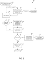
- FIG. 6 is a flowchart 600 of a method of an embodiment for booting from a memory die.
- the CPU 140 executes from the start of virtual memory to load the FSBL (act 605 ). If there are any failures in accessing the first copy of the FSBL, the NAND controller 102 changes the address translation to read from the secondary copy (act 610 ). If there are failures in both copies, the method stops, and an error notification is sent (act 615 ). Otherwise, the working copy of the FSBL is executed (act 620 ). It is then determined if initialization code is required (act 625 )).
- the FSBL loads the initialization code to SRAM 116 , and the CPU 140 starts executing from the start of the initialization code (act 630 ). Otherwise, the CPU 140 initializes all interfaces and scans for boot blocks (act 635 ).
- the FSBL can have instructions to initialize the required interfaces (e.g., the host interface module on the host side, the flash interface module on the memory side, etc.), which helps in interacting with tools or software on the host to enable boot block creation.
- the required interfaces e.g., the host interface module on the host side, the flash interface module on the memory side, etc.
- any suitable type of memory can be used.
- Semiconductor memory devices include volatile memory devices, such as dynamic random access memory (“DRAM”) or static random access memory (“SRAM”) devices, non-volatile memory devices, such as resistive random access memory (“ReRAM”), electrically erasable programmable read only memory (“EEPROM”), flash memory (which can also be considered a subset of EEPROM), ferroelectric random access memory (“FRAM”), and magnetoresistive random access memory (“MRAM”), and other semiconductor elements capable of storing information.
- volatile memory devices such as dynamic random access memory (“DRAM”) or static random access memory (“SRAM”) devices
- non-volatile memory devices such as resistive random access memory (“ReRAM”), electrically erasable programmable read only memory (“EEPROM”), flash memory (which can also be considered a subset of EEPROM), ferroelectric random access memory (“FRAM”), and magnetoresistive random access memory (“MRAM”), and other semiconductor elements capable of storing information.
- ReRAM resistive random access memory
- the memory devices can be formed from passive and/or active elements, in any combinations.
- passive semiconductor memory elements include ReRAM device elements, which in some embodiments include a resistivity switching storage element, such as an anti-fuse, phase change material, etc., and optionally a steering element, such as a diode, etc.
- active semiconductor memory elements include EEPROM and flash memory device elements, which in some embodiments include elements containing a charge storage region, such as a floating gate, conductive nanoparticles, or a charge storage dielectric material.
- Multiple memory elements may be configured so that they are connected in series or so that each element is individually accessible.
- flash memory devices in a NAND configuration typically contain memory elements connected in series.
- a NAND memory array may be configured so that the array is composed of multiple strings of memory in which a string is composed of multiple memory elements sharing a single bit line and accessed as a group.
- memory elements may be configured so that each element is individually accessible, e.g., a NOR memory array.
- NAND and NOR memory configurations are examples, and memory elements may be otherwise configured.
- the semiconductor memory elements located within and/or over a substrate may be arranged in two or three dimensions, such as a two dimensional memory structure or a three dimensional memory structure.
- the semiconductor memory elements are arranged in a single plane or a single memory device level.
- memory elements are arranged in a plane (e.g., in an x-z direction plane) which extends substantially parallel to a major surface of a substrate that supports the memory elements.
- the substrate may be a wafer over or in which the layer of the memory elements are formed or it may be a carrier substrate which is attached to the memory elements after they are formed.
- the substrate may include a semiconductor such as silicon.
- the memory elements may be arranged in the single memory device level in an ordered array, such as in a plurality of rows and/or columns. However, the memory elements may be arrayed in non-regular or non-orthogonal configurations.
- the memory elements may each have two or more electrodes or contact lines, such as bit lines and wordlines.
- a three dimensional memory array is arranged so that memory elements occupy multiple planes or multiple memory device levels, thereby forming a structure in three dimensions (i.e., in the x, y and z directions, where the y direction is substantially perpendicular and the x and z directions are substantially parallel to the major surface of the substrate).
- a three dimensional memory structure may be vertically arranged as a stack of multiple two dimensional memory device levels.
- a three dimensional memory array may be arranged as multiple vertical columns (e.g., columns extending substantially perpendicular to the major surface of the substrate, i.e., in the y direction) with each column having multiple memory elements in each column.
- the columns may be arranged in a two dimensional configuration, e.g., in an x-z plane, resulting in a three dimensional arrangement of memory elements with elements on multiple vertically stacked memory planes.
- Other configurations of memory elements in three dimensions can also constitute a three dimensional memory array.
- the memory elements may be coupled together to form a NAND string within a single horizontal (e.g., x-z) memory device levels.
- the memory elements may be coupled together to form a vertical NAND string that traverses across multiple horizontal memory device levels.
- Other three dimensional configurations can be envisioned wherein some NAND strings contain memory elements in a single memory level while other strings contain memory elements which span through multiple memory levels.
- Three dimensional memory arrays may also be designed in a NOR configuration and in a ReRAM configuration.
- a monolithic three dimensional memory array typically, one or more memory device levels are formed above a single substrate.
- the monolithic three dimensional memory array may also have one or more memory layers at least partially within the single substrate.
- the substrate may include a semiconductor such as silicon.
- the layers constituting each memory device level of the array are typically formed on the layers of the underlying memory device levels of the array.
- layers of adjacent memory device levels of a monolithic three dimensional memory array may be shared or have intervening layers between memory device levels.
- non-monolithic stacked memories can be constructed by forming memory levels on separate substrates and then stacking the memory levels atop each other. The substrates may be thinned or removed from the memory device levels before stacking, but as the memory device levels are initially formed over separate substrates, the resulting memory arrays are not monolithic three dimensional memory arrays. Further, multiple two dimensional memory arrays or three dimensional memory arrays (monolithic or non-monolithic) may be formed on separate chips and then packaged together to form a stacked-chip memory device.
- Associated circuitry is typically required for operation of the memory elements and for communication with the memory elements.
- memory devices may have circuitry used for controlling and driving memory elements to accomplish functions such as programming and reading.
- This associated circuitry may be on the same substrate as the memory elements and/or on a separate substrate.
- a controller for memory read-write operations may be located on a separate controller chip and/or on the same substrate as the memory elements.
Abstract
Description
Claims (16)
Priority Applications (2)
| Application Number | Priority Date | Filing Date | Title |
|---|---|---|---|
| US16/732,649 US11237838B2 (en) | 2020-01-02 | 2020-01-02 | Storage system and method for enabling a direct accessible boot block in a memory die |
| PCT/US2020/037743 WO2021137890A1 (en) | 2020-01-02 | 2020-06-15 | Storage system and method for enabling a direct accessible boot block in a memory die |
Applications Claiming Priority (1)
| Application Number | Priority Date | Filing Date | Title |
|---|---|---|---|
| US16/732,649 US11237838B2 (en) | 2020-01-02 | 2020-01-02 | Storage system and method for enabling a direct accessible boot block in a memory die |
Publications (2)
| Publication Number | Publication Date |
|---|---|
| US20210208900A1 US20210208900A1 (en) | 2021-07-08 |
| US11237838B2 true US11237838B2 (en) | 2022-02-01 |
Family
ID=76654397
Family Applications (1)
| Application Number | Title | Priority Date | Filing Date |
|---|---|---|---|
| US16/732,649 Active 2040-01-08 US11237838B2 (en) | 2020-01-02 | 2020-01-02 | Storage system and method for enabling a direct accessible boot block in a memory die |
Country Status (2)
| Country | Link |
|---|---|
| US (1) | US11237838B2 (en) |
| WO (1) | WO2021137890A1 (en) |
Citations (21)
| Publication number | Priority date | Publication date | Assignee | Title |
|---|---|---|---|---|
| US20030005278A1 (en) | 2001-06-30 | 2003-01-02 | Guoshun Deng | Multifunction semiconductor storage device and a method for booting-up computer host |
| US6615404B1 (en) * | 1999-05-13 | 2003-09-02 | Tadiran Telecom Business Systems Ltd. | Method and apparatus for downloading software into an embedded-system |
| US20040076069A1 (en) | 2002-10-21 | 2004-04-22 | Microsoft Corporation | System and method for initializing a memory device from block oriented NAND flash |
| US20040139307A1 (en) | 2003-01-09 | 2004-07-15 | Barnett Philip C. | Method and apparatus for initializing a semiconductor circuit from an external interface |
| US20040230738A1 (en) | 2003-01-09 | 2004-11-18 | Samsung Electronics Co., Ltd. | Apparatus and method for controlling execute-in-place (XIP) in serial flash memory, and flash memory chip using the same |
| US20050160219A1 (en) * | 2004-01-20 | 2005-07-21 | Samsung Electronics Co., Ltd. | Apparatus and method for booting NAND flash memory of a mobile terminal |
| US20060236198A1 (en) * | 2005-04-01 | 2006-10-19 | Dot Hill Systems Corporation | Storage system with automatic redundant code component failure detection, notification, and repair |
| US20070088940A1 (en) | 2005-10-13 | 2007-04-19 | Sandisk Corporation | Initialization of flash storage via an embedded controller |
| US7734945B1 (en) * | 2005-04-29 | 2010-06-08 | Microsoft Corporation | Automated recovery of unbootable systems |
| US7797693B1 (en) * | 2003-12-12 | 2010-09-14 | Hewlett-Packard Development Company, L.P. | NAND mobile devices capable of updating firmware or software in a manner analogous to NOR mobile devices |
| US20120151202A1 (en) | 2010-12-14 | 2012-06-14 | International Business Machines Corporation | Management of multiple software images with shared memory blocks |
| US8589730B2 (en) * | 2010-08-31 | 2013-11-19 | Apple Inc. | Handling errors during device bootup from a non-volatile memory |
| US20140013097A1 (en) * | 2006-04-10 | 2014-01-09 | Apple Inc. | Retrieving Boot Instructions From Nonvolatile Memory |
| US20140089655A1 (en) * | 2011-02-14 | 2014-03-27 | Timothy M. Lambert | System and method for auto-failover and version matching of bootloader in an access controller |
| US20140095927A1 (en) * | 2010-07-23 | 2014-04-03 | Brocade Communications Systems, Inc. | Achieving ultra-high availability using a single cpu |
| US20160154700A1 (en) * | 2014-11-28 | 2016-06-02 | Huawei Technologies Co., Ltd. | Startup Method and Apparatus and Computer System |
| US9485379B2 (en) * | 2013-07-31 | 2016-11-01 | Kyocera Document Solutions Inc. | Image forming apparatus including auxiliary storage part limited in the number of times rewriting, image forming method, and recording medium |
| US9734117B2 (en) | 2015-01-26 | 2017-08-15 | Western Digital Technologies, Inc. | Data storage device and method for integrated bridge firmware to be retrieved from a storage system on chip (SOC) |
| US20190163620A1 (en) * | 2017-11-27 | 2019-05-30 | Western Digital Technologies, Inc. | Handling of unaligned writes |
| US20190370168A1 (en) * | 2018-05-31 | 2019-12-05 | Western Digital Technologies, Inc. | Storage System and Method for Soft-Decision-Based Command Execution to Enhance Random Write Performance |
| US20200379643A1 (en) * | 2019-05-29 | 2020-12-03 | Western Digital Technologies, Inc. | Storage System and Method for Storage System Calibration |
-
2020
- 2020-01-02 US US16/732,649 patent/US11237838B2/en active Active
- 2020-06-15 WO PCT/US2020/037743 patent/WO2021137890A1/en active Application Filing
Patent Citations (24)
| Publication number | Priority date | Publication date | Assignee | Title |
|---|---|---|---|---|
| US6615404B1 (en) * | 1999-05-13 | 2003-09-02 | Tadiran Telecom Business Systems Ltd. | Method and apparatus for downloading software into an embedded-system |
| US20030005278A1 (en) | 2001-06-30 | 2003-01-02 | Guoshun Deng | Multifunction semiconductor storage device and a method for booting-up computer host |
| US20040076069A1 (en) | 2002-10-21 | 2004-04-22 | Microsoft Corporation | System and method for initializing a memory device from block oriented NAND flash |
| US20040139307A1 (en) | 2003-01-09 | 2004-07-15 | Barnett Philip C. | Method and apparatus for initializing a semiconductor circuit from an external interface |
| US20040230738A1 (en) | 2003-01-09 | 2004-11-18 | Samsung Electronics Co., Ltd. | Apparatus and method for controlling execute-in-place (XIP) in serial flash memory, and flash memory chip using the same |
| US7797693B1 (en) * | 2003-12-12 | 2010-09-14 | Hewlett-Packard Development Company, L.P. | NAND mobile devices capable of updating firmware or software in a manner analogous to NOR mobile devices |
| US20050160219A1 (en) * | 2004-01-20 | 2005-07-21 | Samsung Electronics Co., Ltd. | Apparatus and method for booting NAND flash memory of a mobile terminal |
| US20060236198A1 (en) * | 2005-04-01 | 2006-10-19 | Dot Hill Systems Corporation | Storage system with automatic redundant code component failure detection, notification, and repair |
| US7734945B1 (en) * | 2005-04-29 | 2010-06-08 | Microsoft Corporation | Automated recovery of unbootable systems |
| US20070088940A1 (en) | 2005-10-13 | 2007-04-19 | Sandisk Corporation | Initialization of flash storage via an embedded controller |
| US20140013097A1 (en) * | 2006-04-10 | 2014-01-09 | Apple Inc. | Retrieving Boot Instructions From Nonvolatile Memory |
| US20140095927A1 (en) * | 2010-07-23 | 2014-04-03 | Brocade Communications Systems, Inc. | Achieving ultra-high availability using a single cpu |
| US9026848B2 (en) * | 2010-07-23 | 2015-05-05 | Brocade Communications Systems, Inc. | Achieving ultra-high availability using a single CPU |
| US8589730B2 (en) * | 2010-08-31 | 2013-11-19 | Apple Inc. | Handling errors during device bootup from a non-volatile memory |
| US20120151202A1 (en) | 2010-12-14 | 2012-06-14 | International Business Machines Corporation | Management of multiple software images with shared memory blocks |
| US20140089655A1 (en) * | 2011-02-14 | 2014-03-27 | Timothy M. Lambert | System and method for auto-failover and version matching of bootloader in an access controller |
| US9485379B2 (en) * | 2013-07-31 | 2016-11-01 | Kyocera Document Solutions Inc. | Image forming apparatus including auxiliary storage part limited in the number of times rewriting, image forming method, and recording medium |
| US20160154700A1 (en) * | 2014-11-28 | 2016-06-02 | Huawei Technologies Co., Ltd. | Startup Method and Apparatus and Computer System |
| US9734117B2 (en) | 2015-01-26 | 2017-08-15 | Western Digital Technologies, Inc. | Data storage device and method for integrated bridge firmware to be retrieved from a storage system on chip (SOC) |
| US20190163620A1 (en) * | 2017-11-27 | 2019-05-30 | Western Digital Technologies, Inc. | Handling of unaligned writes |
| US10372603B2 (en) * | 2017-11-27 | 2019-08-06 | Western Digital Technologies, Inc. | Handling of unaligned writes |
| US20190370168A1 (en) * | 2018-05-31 | 2019-12-05 | Western Digital Technologies, Inc. | Storage System and Method for Soft-Decision-Based Command Execution to Enhance Random Write Performance |
| US10725901B2 (en) * | 2018-05-31 | 2020-07-28 | Western Digital Technologies, Inc. | Storage system and method for soft-decision-based command execution to enhance random write performance |
| US20200379643A1 (en) * | 2019-05-29 | 2020-12-03 | Western Digital Technologies, Inc. | Storage System and Method for Storage System Calibration |
Non-Patent Citations (3)
| Title |
|---|
| International Search Report dated Oct. 27, 2020 for International Application No. PCT/US2020/037743. |
| Written Opinion dated Oct. 27, 2020 for International Application No. PCT/US2020/037743. |
| Ye, Roger; "Embedded Ptogramming with Android: Using U-Boot to Boot the Goldfish Kernel"; Informit; Chapter from Embedded Programming with Android; Bringing Up an Android System from Scratch; downloaded from the Internet on Sep. 12, 2019 at http://www.informit.com/articles/printerfriendly/2431471; 21 pages; Sep. 1, 2015. |
Also Published As
| Publication number | Publication date |
|---|---|
| US20210208900A1 (en) | 2021-07-08 |
| WO2021137890A1 (en) | 2021-07-08 |
Similar Documents
| Publication | Publication Date | Title |
|---|---|---|
| US9606865B2 (en) | Method and apparatus for configuring a memory device | |
| CN109284202B (en) | Controller and operation method thereof | |
| US9329931B2 (en) | Solid state drive emergency pre-boot application providing expanded data recovery function | |
| US20160232057A1 (en) | Safe mode boot loader | |
| KR102612842B1 (en) | Apparatus and method for retaining firmware in memory system | |
| US9905314B2 (en) | Storage module and method for datapath bypass | |
| US20170249155A1 (en) | Memory System and Method for Fast Firmware Download | |
| CN109935251B (en) | Memory system, method of operating the same, and data processing system including the same | |
| US9940039B2 (en) | Method and data storage device with enhanced data retention | |
| WO2020242530A1 (en) | Storage system and method for storage system calibration | |
| CN110196822B (en) | Memory device, memory controller, memory system, and operating method thereof | |
| US11663081B2 (en) | Storage system and method for data recovery after detection of an uncorrectable error | |
| US11150842B1 (en) | Dynamic memory controller and method for use therewith | |
| CN108986864B (en) | Controller and memory system and operating method of memory system | |
| US11237838B2 (en) | Storage system and method for enabling a direct accessible boot block in a memory die | |
| US11461052B1 (en) | Storage system with dual submission queue doorbell registers and method for use in a multi-tenant system | |
| US11494125B2 (en) | Storage system and method for dual fast release and slow release responses | |
| US11403163B2 (en) | Storage system and method for crash analysis | |
| US11138065B1 (en) | Storage system and method for fast low-density parity check (LDPC) encoding | |
| US11334256B2 (en) | Storage system and method for boundary wordline data retention handling | |
| WO2020242531A1 (en) | Host and method for storage system calibration | |
| US11537325B2 (en) | Storage system and method for token provisioning for faster data access | |
| US20230385068A1 (en) | Data Storage Device and Method for Storage-Class-Memory-Accelerated Boot Partition Optimization | |
| US20220187996A1 (en) | Memory controller and storage device including same | |
| US11550662B2 (en) | Storage device and computing system |
Legal Events
| Date | Code | Title | Description |
|---|---|---|---|
| AS | Assignment |
Owner name: WESTERN DIGITAL TECHNOLOGIES, INC., CALIFORNIA Free format text: ASSIGNMENT OF ASSIGNORS INTEREST;ASSIGNORS:PAMOTI, VENKATESH NAIDU;MUTHIAH, RAMANATHAN;RAJAKUMAR, GNANASEKAR;SIGNING DATES FROM 20200101 TO 20200102;REEL/FRAME:051402/0542 |
|
| FEPP | Fee payment procedure |
Free format text: ENTITY STATUS SET TO UNDISCOUNTED (ORIGINAL EVENT CODE: BIG.); ENTITY STATUS OF PATENT OWNER: LARGE ENTITY |
|
| AS | Assignment |
Owner name: JPMORGAN CHASE BANK, N.A., AS AGENT, ILLINOIS Free format text: SECURITY INTEREST;ASSIGNOR:WESTERN DIGITAL TECHNOLOGIES, INC.;REEL/FRAME:052025/0088 Effective date: 20200211 |
|
| STPP | Information on status: patent application and granting procedure in general |
Free format text: NON FINAL ACTION MAILED |
|
| STPP | Information on status: patent application and granting procedure in general |
Free format text: RESPONSE TO NON-FINAL OFFICE ACTION ENTERED AND FORWARDED TO EXAMINER |
|
| STPP | Information on status: patent application and granting procedure in general |
Free format text: NOTICE OF ALLOWANCE MAILED -- APPLICATION RECEIVED IN OFFICE OF PUBLICATIONS |
|
| STPP | Information on status: patent application and granting procedure in general |
Free format text: PUBLICATIONS -- ISSUE FEE PAYMENT VERIFIED |
|
| STPP | Information on status: patent application and granting procedure in general |
Free format text: AWAITING TC RESP, ISSUE FEE PAYMENT VERIFIED |
|
| STPP | Information on status: patent application and granting procedure in general |
Free format text: PUBLICATIONS -- ISSUE FEE PAYMENT VERIFIED |
|
| STCF | Information on status: patent grant |
Free format text: PATENTED CASE |
|
| AS | Assignment |
Owner name: WESTERN DIGITAL TECHNOLOGIES, INC., CALIFORNIA Free format text: RELEASE OF SECURITY INTEREST AT REEL 052025 FRAME 0088;ASSIGNOR:JPMORGAN CHASE BANK, N.A.;REEL/FRAME:058965/0699 Effective date: 20220203 |
|
| AS | Assignment |
Owner name: JPMORGAN CHASE BANK, N.A., ILLINOIS Free format text: PATENT COLLATERAL AGREEMENT - A&R LOAN AGREEMENT;ASSIGNOR:WESTERN DIGITAL TECHNOLOGIES, INC.;REEL/FRAME:064715/0001 Effective date: 20230818 |