JP5284488B2 - Recording head and manufacturing method thereof - Google Patents
Recording head and manufacturing method thereof Download PDFInfo
- Publication number
- JP5284488B2 JP5284488B2 JP2011545029A JP2011545029A JP5284488B2 JP 5284488 B2 JP5284488 B2 JP 5284488B2 JP 2011545029 A JP2011545029 A JP 2011545029A JP 2011545029 A JP2011545029 A JP 2011545029A JP 5284488 B2 JP5284488 B2 JP 5284488B2
- Authority
- JP
- Japan
- Prior art keywords
- wiring board
- electric wiring
- recording element
- insulator
- recording head
- Prior art date
- Legal status (The legal status is an assumption and is not a legal conclusion. Google has not performed a legal analysis and makes no representation as to the accuracy of the status listed.)
- Expired - Fee Related
Links
Images


Classifications
-
- B—PERFORMING OPERATIONS; TRANSPORTING
- B41—PRINTING; LINING MACHINES; TYPEWRITERS; STAMPS
- B41J—TYPEWRITERS; SELECTIVE PRINTING MECHANISMS, i.e. MECHANISMS PRINTING OTHERWISE THAN FROM A FORME; CORRECTION OF TYPOGRAPHICAL ERRORS
- B41J2/00—Typewriters or selective printing mechanisms characterised by the printing or marking process for which they are designed
- B41J2/005—Typewriters or selective printing mechanisms characterised by the printing or marking process for which they are designed characterised by bringing liquid or particles selectively into contact with a printing material
- B41J2/01—Ink jet
- B41J2/135—Nozzles
- B41J2/14—Structure thereof only for on-demand ink jet heads
- B41J2/14016—Structure of bubble jet print heads
- B41J2/14072—Electrical connections, e.g. details on electrodes, connecting the chip to the outside...
-
- B—PERFORMING OPERATIONS; TRANSPORTING
- B41—PRINTING; LINING MACHINES; TYPEWRITERS; STAMPS
- B41J—TYPEWRITERS; SELECTIVE PRINTING MECHANISMS, i.e. MECHANISMS PRINTING OTHERWISE THAN FROM A FORME; CORRECTION OF TYPOGRAPHICAL ERRORS
- B41J2/00—Typewriters or selective printing mechanisms characterised by the printing or marking process for which they are designed
- B41J2/005—Typewriters or selective printing mechanisms characterised by the printing or marking process for which they are designed characterised by bringing liquid or particles selectively into contact with a printing material
- B41J2/01—Ink jet
- B41J2/135—Nozzles
- B41J2/16—Production of nozzles
- B41J2/1601—Production of bubble jet print heads
- B41J2/1603—Production of bubble jet print heads of the front shooter type
-
- B—PERFORMING OPERATIONS; TRANSPORTING
- B41—PRINTING; LINING MACHINES; TYPEWRITERS; STAMPS
- B41J—TYPEWRITERS; SELECTIVE PRINTING MECHANISMS, i.e. MECHANISMS PRINTING OTHERWISE THAN FROM A FORME; CORRECTION OF TYPOGRAPHICAL ERRORS
- B41J2/00—Typewriters or selective printing mechanisms characterised by the printing or marking process for which they are designed
- B41J2/005—Typewriters or selective printing mechanisms characterised by the printing or marking process for which they are designed characterised by bringing liquid or particles selectively into contact with a printing material
- B41J2/01—Ink jet
- B41J2/135—Nozzles
- B41J2/16—Production of nozzles
- B41J2/1621—Manufacturing processes
- B41J2/1623—Manufacturing processes bonding and adhesion
-
- Y—GENERAL TAGGING OF NEW TECHNOLOGICAL DEVELOPMENTS; GENERAL TAGGING OF CROSS-SECTIONAL TECHNOLOGIES SPANNING OVER SEVERAL SECTIONS OF THE IPC; TECHNICAL SUBJECTS COVERED BY FORMER USPC CROSS-REFERENCE ART COLLECTIONS [XRACs] AND DIGESTS
- Y10—TECHNICAL SUBJECTS COVERED BY FORMER USPC
- Y10T—TECHNICAL SUBJECTS COVERED BY FORMER US CLASSIFICATION
- Y10T29/00—Metal working
- Y10T29/49—Method of mechanical manufacture
- Y10T29/49401—Fluid pattern dispersing device making, e.g., ink jet
Landscapes
- Engineering & Computer Science (AREA)
- Manufacturing & Machinery (AREA)
- Particle Formation And Scattering Control In Inkjet Printers (AREA)
Description
本発明は、記録媒体に記録を行うための記録ヘッドとその製造方法に関する。 The present invention relates to a recording head for recording on a recording medium and a manufacturing method thereof.
記録ヘッドとして代表的なインクジェット記録ヘッドは、一般的に、インク(液体)を吐出する記録素子基板と、インクを収納する容器であるインクタンクと、記録素子基板に吐出制御信号や吐出のための電力を伝達する電気配線基板とで構成されている。記録素子基板は、保持部材としてのインクタンクに固定されており、電気配線基板もインクタンクに固定されている。 A typical inkjet recording head as a recording head generally includes a recording element substrate that ejects ink (liquid), an ink tank that is a container for storing ink, and an ejection control signal and ejection for the recording element substrate. It is comprised with the electric wiring board which transmits electric power. The recording element substrate is fixed to an ink tank as a holding member, and the electric wiring substrate is also fixed to the ink tank.
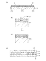
図8は、従来の電気配線基板H2000の接着固定を示している図である。 FIG. 8 is a diagram showing adhesion and fixing of a conventional electric wiring board H2000.
図8(a)は、インクジェット記録ヘッドを記録素子基板H1000側から見た図である。なお、図8(a)は、説明のために、配線H2002を透かして見えるように記載してある。図8(b)は、図8(a)のX-X断面を示している。また、図8(c)は、図8(b)のA部の拡大図である。 FIG. 8A is a diagram of the ink jet recording head viewed from the recording element substrate H1000 side. Note that FIG. 8A is illustrated so that the wiring H2002 can be seen through for the purpose of explanation. FIG. 8B shows an XX cross section of FIG. Moreover, FIG.8 (c) is an enlarged view of the A section of FIG.8 (b).
図8(a)に示すように、電気配線基板H2000の有する開口部H2003の内側に、記録素子基板H1000が収められており、電気配線基板H2000及び記録素子基板H1000はインクタンクH3000に固定されている。 As shown in FIG. 8A, the recording element substrate H1000 is accommodated inside the opening H2003 of the electric wiring substrate H2000, and the electric wiring substrate H2000 and the recording element substrate H1000 are fixed to the ink tank H3000. Yes.
電気配線基板H2000は図8(c)に示すように、絶縁体からなる第1のフィルムH2010、第2のフィルムH2020、配線H2002を有する配線層H2030とで構成される層状となっている。この配線H2002は、その一端において記録素子基板H1000に接続されており、インクジェット記録ヘッドの搭載される本体からの制御信号や電力を記録素子基板H1000に伝達する。 As shown in FIG. 8C, the electric wiring board H2000 has a layer structure including a first film H2010 made of an insulator, a second film H2020, and a wiring layer H2030 having a wiring H2002. The wiring H2002 is connected to the recording element substrate H1000 at one end thereof, and transmits a control signal and power from the main body on which the ink jet recording head is mounted to the recording element substrate H1000.
一般的に、電気配線基板H2000は、接着剤H4100によってインクタンクH3000に固定されており、更に電気配線基板H2000の外周は、封止剤H4000によって封止されている(特許文献1)。 In general, the electric wiring board H2000 is fixed to the ink tank H3000 by an adhesive H4100, and the outer periphery of the electric wiring board H2000 is sealed with a sealing agent H4000 (Patent Document 1).
しかし、接着剤を塗布することで電気配線基板を保持部材に固定する従来の方法では、接着剤の塗布のばらつき等により電気配線基板の端部まで接着剤が塗布されない場合がある。 However, in the conventional method of fixing the electric wiring board to the holding member by applying an adhesive, the adhesive may not be applied to the end of the electric wiring board due to variations in the application of the adhesive.
図9(a)に示すように、接着剤H4100による固定で電気配線基板の端部まで接着されていないために、電気配線基板H2000の端部がインクタンクH3000から浮いた状態となってしまうことがある。この状態で記録を行うために記録ヘッドを走査すると、図9(b)に示すように、紙などの記録媒体Pと接触して電気配線基板が捲れてしまう可能性がある。その場合、記録素子基板に電気信号が送られなくなり、記録ヘッドの吐出の機能が失われる恐れがある。近年は、記録媒体の種類が増えているが、特に腰の強い記録媒体を用いて印刷する場合は、電気配線基板が捲れてしまう可能性が高い。 As shown in FIG. 9A, the end of the electric wiring board H2000 is lifted from the ink tank H3000 because the end of the electric wiring board is not bonded to the end by fixing with the adhesive H4100. There is. When the recording head is scanned in order to perform recording in this state, as shown in FIG. 9B, there is a possibility that the electric wiring board may be rolled up in contact with the recording medium P such as paper. In that case, an electric signal cannot be sent to the recording element substrate, and the ejection function of the recording head may be lost. In recent years, the number of types of recording media has increased. However, when printing is performed using a particularly stiff recording medium, there is a high possibility that the electrical wiring board will be rolled up.
本発明の記録ヘッドの製造方法は、液体を吐出するために利用されるエネルギーを発生する記録素子を有する記録素子基板と、前記記録素子基板を内部に配置するための開口部と、前記記録素子と電気的に接続される複数の配線と、前記複数の配線を挟む、膜状の第1の絶縁体及び第2の絶縁体と、前記複数の配線の間に配され、前記第1の絶縁体と前記第2の絶縁体とを接着する接着剤と、を有する電気配線基板と、前記記録素子基板を保持するための保持部材と、を有する記録ヘッドの製造方法であって、前記保持部材はレーザー光に対して吸収性を有し、前記第1の絶縁体、前記第2の絶縁体、及び前記接着剤はレーザー光に対して透過性を有しており、前記保持部材の前記記録素子基板が固定される面と前記電気配線基板とを、前記電気配線基板の外周部の少なくとも一部で当接させ、該当接がなされた当接部に向けて、前記電気配線基板のうち、前記配線が配置されていない部分を介してレーザー光を照射することにより、前記電気配線基板と前記保持部材とを溶着することを特徴とする。 Method of manufacturing a recording head of the present invention, an opening for placing the recording element substrate having a recording element for generating energy to be utilized for discharging liquid, the recording element substrate therein, the recording element sandwiching and electrically connected to the plurality Ru wirings, a plurality of wiring and the first insulator and the second insulator film shape, disposed between the plurality of wires, said first insulating and the electric wiring board having an adhesive for bonding the said the body the second insulator, and a manufacturing method of the recording head to have a, a holding member for holding said recording element substrate, the holding The member has absorptivity with respect to laser light, and the first insulator, the second insulator, and the adhesive have transparency with respect to laser light, and the holding member the surface on which the recording element substrate Ru is fixed and said electric wiring board, wherein Brought into contact with at least a portion of the outer peripheral portion of the gas-wiring board, toward the abutment the abutment is made, among the electric wiring substrate is irradiated with laser light through a portion where the wiring is not arranged Thus, the electric wiring board and the holding member are welded.
レーザー光を照射することによって、電気配線基板の外周の少なくとも一部で、電気配線基板を保持部材に固定する。これにより、保持部材に対して電気配線基板の端部まで精度よく電気配線基板を接合することが可能であり、記録媒体の接触による電気配線基板の捲れの恐れを低減し、記録ヘッドの電気的信頼性を向上することができる。 By irradiating the laser beam, the electric wiring board is fixed to the holding member at least at a part of the outer periphery of the electric wiring board. As a result, the electric wiring board can be accurately bonded to the holding member up to the end of the electric wiring board, the risk of the electric wiring board being bent due to the contact with the recording medium is reduced, and the electrical Reliability can be improved.
(第1の実施形態)
次に、本発明の実施形態を図1〜図5を用いて説明する。(First embodiment)
Next, an embodiment of the present invention will be described with reference to FIGS.
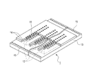
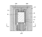
図2(a)は、本発明を適用可能なインクジェット記録ヘッド1の概略模式図であり、図2(b)はその分解模式図である。インクジェット記録ヘッド1は、記録素子基板10、電気配線基板20、インクタンク30とで構成される。記録素子基板10は保持部材としてのインクタンク30の一面(第1の面31)に固定されており、インクタンク30のこの第1の面31に電気配線基板20も固定されている。
FIG. 2A is a schematic diagram of an inkjet recording head 1 to which the present invention can be applied, and FIG. 2B is an exploded schematic diagram thereof. The ink jet recording head 1 includes a
インクジェット記録ヘッド1は、インクジェット記録装置に設置されているキャリッジの位置決め手段によって固定支持されるとともに、キャリッジに対して着脱可能となっている。 The ink jet recording head 1 is fixedly supported by a carriage positioning means installed in the ink jet recording apparatus, and is detachable from the carriage.
記録素子基板10は、液体(インク)を吐出する吐出口と、インクを吐出するための記録素子を有している。インクジェット記録ヘッド1は、インクジェット記録装置から送られる電気信号に応じて、インクを吐出するために利用されるエネルギーを発生する記録素子を駆動する。これにより、インク(液体)を収容するインクタンク30から供給されるインクを吐出口から吐出し、記録媒体に記録を行う。記録素子としては、発熱抵抗素子やピエゾ素子などが挙げられる。
The
図3は、記録素子基板10の構成を説明するために一部を切断した斜視図である。
FIG. 3 is a perspective view in which a part of the
記録素子基板10は、インクを吐出するための吐出口11、吐出口11と連通して吐出口11にインクを供給するためのインク供給口12とを有する。インク供給口12はシリコン基板13に形成される。
The
シリコン基板13は、厚さ0.5mm〜1.0mmを有しており、異方性エッチングによりインク供給口12が形成される。また、シリコン基板13上には、記録素子としての発熱抵抗素子14が形成され、その発熱抵抗素子14と吐出口11とが対応するように、シリコン基板13上にフォトリソグラフィー技術を用いて、吐出口11が形成される。さらにシリコン基板13上には発熱抵抗素子14を駆動するための電気信号や電力を供給するための電極部としてAu等のバンプ15が設けられている。
The
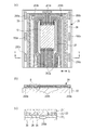
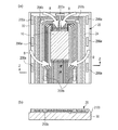
次に、図1を用いて電気配線基板20について説明する。図1(a)は、インクジェット記録ヘッドを記録素子基板10側から見た図である。なお、図1(a)は、説明のために配線24を透かして描いた図となっており、以降のインクジェット記録ヘッドを記録素子基板10側から見た図も同様に記載している。図1(b)は、図1(a)のY-Y断面を示している。また、図1(c)は、図1(b)のB部の拡大図である。
Next, the
記録素子基板10には、電気配線基板20が電気的に接続されており、この電気配線基板20を介して記録素子基板10の有する発熱抵抗素子14に電気信号が送られる。電気配線基板20に設けられた開口部26に収まるようにして、記録素子基板10が配置されている。
An
電気配線基板20は図1(c)に示すように、膜状の絶縁体からなる第1のフィルム21(第1の絶縁体)及び第2のフィルム22(第2の絶縁体)、配線24を有する配線層23で構成される層状である。第1のフィルム21及び第2のフィルム22は配線24を挟むことで保護している。配線層23は、配線24の隙間を埋めることと、第1のフィルム21、第2のフィルム22と配線層23とを接着する目的で、接着剤25が塗布されている。配線24は、例えばCuなどの導電性の良い金属製で、印字制御に必要な本数が並列に配置されている(簡略化のため本数を減らして図示)。この配線24は、その一端が記録素子基板10のバンプ15に接続されており、インクジェット記録ヘッド1が搭載されるインクジェット記録装置からの制御信号や電力を、記録素子基板10に伝達している。
As shown in FIG. 1C, the
また、図1(b)に示すように、配線24の他端は、インクジェット記録装置からの信号を受け取るために電気配線基板20に設けられた信号入力端子27に接続される。電気配線基板20のうち、記録素子基板10を収めるための開口部26が設けられた部分はインクタンク30の第1の面31に、信号入力端子27が設けられた部分は第1の面31とは異なる第2の面32に対して固定される。すなわち、電気配線基板20は、第1の面31から第2の面32に向かって屈曲する屈曲部28を有している。
Further, as shown in FIG. 1B, the other end of the
次に、本実施形態における電気配線基板20のインクタンク30への固定について説明する。
Next, fixing of the
本発明は、レーザー光を用いて、電気配線基板20をインクタンク30に対して固定する。したがって、本実施形態では、インクタンク30をレーザー光に対して吸収性を有する部材とし、電気配線基板20の配線24以外の部分である、第1のフィルム21、第2のフィルム22、及び接着剤25を透過性を有する部材とする。
In the present invention, the
次に、本実施形態の記録ヘッドのレーザー光を用いた製造方法に関して説明する。 Next, a manufacturing method using laser light for the recording head of this embodiment will be described.
まず、電気配線基板20とインクタンク30とを、溶着する面を内側にして当接する。次に、電気配線基板20のうち、透過性を有している第1のフィルム21、第2のフィルム22、及び接着剤25を介して、第2のフィルム22とインクタンク30とが当接する当接部に向けてレーザー光を照射する。筐体であるインクタンク30ではなく、薄い層状である電気配線基板20を介してレーザー光を照射するため、容易にレーザー光を照射することが可能である。
First, the
レーザー光が照射されることにより、吸収性を有する部材であるインクタンク30が含有している染料または顔料が発熱して溶融し、この発生した熱は第2のフィルム22に伝達される。第2のフィルムとしてインクタンク30の融点に近い融点を有する材料を用いることで、伝達された熱によって第2のフィルム22も溶融し、当接部は溶着部となり、電気配線基板20とインクタンク30とが接合される。
By irradiating the laser beam, the dye or pigment contained in the
次に、電気配線基板20とインクタンク30とがレーザー光によって溶着される位置について図1を用いて説明する。
Next, the position where the
200(200a、200b)は、レーザー光の照射によってインクタンク30と電気配線基板20とが溶着された部分(溶着部)を示している。金属製である配線24はレーザー光を透過しないため、溶着部200は配線24が配置されていない領域に対応する部分に設けられる。溶着部200aは、溶着部200のうち、電気配線基板20の外周部の端部に形成された溶着部であり、電気配線基板20の外周部の端部に点在して形成されている。
Reference numeral 200 (200a, 200b) denotes a portion (welded portion) where the
レーザー光を用いて部材同士を溶着すると、所望の位置における溶着が可能である。そのため、レーザー光を用いて電気配線基板20とインクタンク30とを溶着すると、電気配線基板20の端部まで精度よく、電気配線基板20をインクタンク30に接合することが可能である。したがって、レーザー光によって電気配線基板20の外周部に溶着部200aを形成することで、印刷時において紙などの記録媒体が電気配線基板20に接触して捲れる可能性を低減し、記録ヘッドの電気的信頼性を向上することが可能である。
When members are welded using laser light, welding at a desired position is possible. Therefore, when the
記録媒体による電気配線基板20の捲れの問題は、電気配線基板20の外周部のうち、記録ヘッドが走査される方向(図1(a)の矢印Aの方向)に関する電気配線基板20の端部や、電気配線基板20の隅の部分で生じ易い。そのため、電気配線基板20の外周部のうち、これらの部分の近傍に溶着部200aを設けると、上記の問題に対してより効果的な構成とすることが可能である。
The problem of the
また、従来の接着剤を用いた方法では、接着剤を硬化するために長時間放置したり、電気配線基板20の外周部を封止剤によって封止したりする必要があったが、本実施形態のようにレーザー光を用いて溶着を行うことで、製造方法にかかる工数を減らすことができる。
Further, in the conventional method using an adhesive, it was necessary to leave the adhesive for a long time to cure the adhesive or to seal the outer peripheral portion of the
さらに、本実施形態では、電気配線基板20のインクタンク30に対する固定の強度を確保するため、配線24の間に対応する部分においても溶着を行っており、溶着部200bが複数形成されている。配線24の間に対応する部分においても溶着することで、外周部の溶着部200aのみで溶着された場合と比較して、インクタンク30に対して電気配線基板20をより確実に固定することが可能である。
Furthermore, in this embodiment, in order to ensure the strength of fixing the
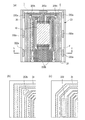
この溶着部200bを設ける位置のより好適な形態について、図4を用いて説明する。図4(a)は、インクジェット記録ヘッドを記録素子基板10側から見た図であり、図4(b)は、図4(a)の波線領域Dを拡大した図である。
A more preferable form of the position where the welded
図4(c)は、記録素子基板10と並列に配置された配線24の間に、溶着部230を設けた図である。このように、電気配線基板20のうち、記録素子基板10と並列に配線24が配置された部分は、記録素子基板10を収めるための開口部26が配置されているために、配線24の配置される密度が他の部分と比較して高い。そのため、電気配線部材20の面積を大きくせずにこの部分に溶着部230を形成するためには、図4(c)のように配線24を細くして溶着するための領域を確保する必要がある。しかし、配線24の幅を細くすると、電気抵抗が大きくなってしまう。
FIG. 4C is a view in which a welded
そこで、図4(a)の領域Dや領域Eのように配線24が屈曲する角の部分において、外側の配線24は直角に屈曲させ、内側の配線24を、溶着部の面積を確保できるように屈曲させた配置とした。そして、確保した領域において溶着部200bを形成した。これにより、配線24を細くする必要がないので、適正な印加電力で使用することができ、より記録ヘッドの耐久性を向上させることが可能となる。
Therefore, the
また、図4(a)の領域Fは、開口部26に対して並列に配線24が配置された部分ではないため、複数の配線24を配置する領域が十分に確保できている。そのため、この部分においても領域Fのように配線24を屈曲させて配置することで、配線24を細くする必要がなくレーザー溶着部200bを設けることが可能である。
4A is not a portion where the
本実施形態では、図4(a)に示すように、領域D、E、Fに配線24を屈曲させて溶着する領域を確保したが、配線24の屈曲の仕方は図で示すものに限定されず、溶着するための領域を確保できるように屈曲させればよい。
In the present embodiment, as shown in FIG. 4A, a region where the
次に、図5を参照して、溶着部200における溶着をより強固なものにするための構成について説明する。 Next, with reference to FIG. 5, the structure for making the welding in the welding part 200 stronger will be described.
レーザー光の照射によって部材同士を溶着して固定する場合では、レーザー照射時における部材同士の当接部の密着性が、固定の強度を左右する。図5(d)は電気配線基板20の層の構造を示す図である。このように内部に金属製の配線24を有する電気配線基板20では、配線24のある場所と配線24の無い接着剤25が埋まっている場所とで若干の厚みの差が生じている。ただし、図5(d)は、厚みの差を誇張している。第2のフィルム22において、配線24の無い薄い部分に対応する部分が溶着される領域である。
In the case where the members are welded and fixed by laser light irradiation, the adhesiveness of the contact portion between the members at the time of laser irradiation affects the fixing strength. FIG. 5D is a diagram showing a layer structure of the
そこで、図5(a)の領域Cの拡大図である図5(b)に示すように、溶着を行う前のインクタンク30のうち溶着される部分に、インクタンク30の第1の面31に対して電気配線基板20と当接する方向に凸である凸形状部33を設けた。これにより、インクタンク30と電気配線基板20とを当接した際に、当接部における密着性を向上させ、部材同士をより強固に固定することが可能となる。
Therefore, as shown in FIG. 5B, which is an enlarged view of the region C in FIG. 5A, the
また、本実施形態では、電気配線基板20の第1のフィルム21、第2のフィルム22、接着剤25を介して、レーザー光を照射する。接着剤25を介するために、レーザー光が当接部に適切に照射されない可能性がある。そこで、より確実に溶着させるためには、電気配線基板20の構造を以下のように工夫することが好ましい。
In the present embodiment, laser light is irradiated through the
例えば、電気配線基板20のうち溶着部に対応する部分には接着剤25がなく空洞である構成や、同じく対応する部分に接着剤25及び第1のフィルムも設けずに第2のフィルムのみ設けた構成が挙げられる。また、電気配線基板20のうち溶着部に対応する部分には接着剤25でなく、レーザー光に対する透過性の高い部材を配した構成とすることで、電気配線基板20の平面性を確保しつつ、より確実に溶着を行うことが可能となる。
For example, the portion corresponding to the welded portion of the
なお、本発明の実施形態において、レーザー光に対して透過性を有する部材とは、部材に対してレーザー光を照射した場合の透過率が30%以上の部材を意味する。また、本発明においてレーザー光に対して吸収性を有する部材とは、部材に対してレーザー光を照射した場合の吸収率が90%以上の部材を意味する。上述のような透過率及び吸収率の部材を用いることで、透過性部材と吸収性部材とのレーザー溶着が可能となる。また、レーザー照射に用いられるレーザー光は、透過性を有する部材を透過可能である波長を有するものであればよい。 In the embodiment of the present invention, the member having transparency to the laser light means a member having a transmittance of 30% or more when the member is irradiated with the laser light. In the present invention, the member having absorptivity to laser light means a member having an absorption rate of 90% or more when the member is irradiated with laser light. By using a member having the above-described transmittance and absorptivity, laser welding between the transmissive member and the absorptive member becomes possible. Moreover, the laser beam used for laser irradiation should just have a wavelength which can permeate | transmit the member which has transparency.
なお、レーザー光の照射方法に関しては、溶着部に沿ってレーザー光を照射するスキャン方式と、溶着部のみにレーザー光が照射可能となるようにマスクを設けて一斉にレーザー光を照射する一括方式とがある。本発明においてはどちらの方法を採用してもよく、レーザーの照射方法は特に限定されない。 Regarding the laser light irradiation method, a scanning method that irradiates laser light along the welded part and a batch method that irradiates the laser light all at once by providing a mask so that only the welded part can be irradiated with laser light. There is. In the present invention, either method may be adopted, and the laser irradiation method is not particularly limited.
本実施形態では、インクタンク30が吸収性を有し、配線24以外の電気配線基板20が透過性を有している。しかし、本発明は、溶着する二つの部材のうち、いずれか一方が吸収性を有し、他方が透過性を有していればよい。本実施形態とは反対に、インクタンク30が透過性を有する場合は、インクタンク30を介してレーザー光を照射するため、電気配線基板20のうち、第2のフィルム22のみが吸収性を有する部材であればよい。また、この場合は、配線24が配置された位置に対応する部分で溶着することも可能であるので、溶着する位置の自由度が増す。
In the present embodiment, the
本実施形態では、インクタンク30と一体である記録ヘッドに関して説明したが、インクタンク30を保持するタンクホルダを有する記録ヘッドであってもよく、この場合は、タンクホルダに記録素子基板及び電気配線基板を接合すればよい。
In this embodiment, the recording head integrated with the
また、電気配線基板20の外周部の一部においてレーザーを用いた溶着を行うことで、記録媒体の接触によって電気配線基板20が捲れてしまう恐れを低減できるので、外周部以外の部分は接着剤を用いて接着する構成であってもよい。
Further, by performing welding using a laser on a part of the outer peripheral portion of the
(第2の実施形態)
次に、本発明の第2の実施形態について図7を用いて説明する。(Second Embodiment)
Next, a second embodiment of the present invention will be described with reference to FIG.
本実施形態は、第1の実施形態のように電気配線部材20の外周部における溶着部を部分的に設けるのではなく、図7に示すように溶着部210を隙間無く繋がるように設けた構成である。その他の構成は第1の実施形態と同様であるので、説明を省略する。
In the present embodiment, the welded
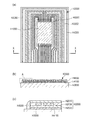
インクジェット記録装置を駆動させると、インクミストなどが電気配線基板20の周囲に付着するが、これらのインクがインクジェット記録ヘッド1に及ぼす課題について図6を用いて説明する。
When the ink jet recording apparatus is driven, ink mist or the like adheres to the periphery of the
図6(a)は、インクジェット記録ヘッド1を記録素子基板10側から見た図である。図6(b)は、図6(a)のZ-Z断面を示している。
FIG. 6A is a diagram of the ink jet recording head 1 as viewed from the
電気配線基板20の周囲に付着したインクI100は、図6(a)のI100で示す矢印Bで示すように電気配線基板20の外周部のうち、溶着部が形成されていない部分から侵入する可能性がある。すなわち、図6(b)に示すように、電気配線基板20とインクタンク30とが溶着されていない隙間に沿って侵入する。この場合に、インクI100は電気配線基板20から露出した配線と記録素子基板10との接続部まで到達し、配線間の不具合を引き起こす恐れがある。
The ink I100 adhering to the periphery of the
そこで、本実施形態では、図7に示すように、インクタンク30の第1の面31に配される電気配線基板20のうち、屈曲部28(図2参照)を除く電気配線基板20の外周部に、レーザー光を照射することで溶着部210が隙間無く形成した構成である。これにより、電気配線基板20とインクタンク30の隙間からインクが侵入し、配線24と記録素子基板10との接続部にインクが付着する恐れを低減することが可能である。したがって、インクジェット記録ヘッドの電気的信頼性を更に向上させることが可能である。
Therefore, in the present embodiment, as shown in FIG. 7, the outer periphery of the
また、本実施形態では、インクジェット記録ヘッドの走査方向に関する電気配線基板20の開口部26の端部についても、同様に隙間のない溶着部220を設けている。これにより、インクが侵入する恐れを更に低減することが可能である。
Further, in the present embodiment, the welded
1 インクジェット記録ヘッド(記録ヘッド)
10 記録素子基板
20 電気配線基板
24 配線
30 インクタンク(保持部材)
200a 溶着部(電気配線基板の外周部に設けられた溶着部)1 Inkjet recording head (recording head)
10
200a welding part (welding part provided in the outer peripheral part of an electric wiring board)
Claims (7)
前記保持部材はレーザー光に対して吸収性を有し、前記第1の絶縁体、前記第2の絶縁体、及び前記接着剤はレーザー光に対して透過性を有しており、
前記保持部材の前記記録素子基板が固定される面と前記電気配線基板とを、前記電気配線基板の外周部の少なくとも一部で当接させ、該当接がなされた当接部に向けて、前記電気配線基板のうち、前記配線が配置されていない部分を介してレーザー光を照射することにより、前記電気配線基板と前記保持部材とを溶着することを特徴とする記録ヘッドの製造方法。 A recording element substrate having a recording element for generating energy to be utilized for discharging liquid and an opening for placement within the recording element substrate, the recording element and electrically connected to Ru plurality of wirings A film-like first insulator and a second insulator sandwiching the plurality of wires, and the first insulator and the second insulator disposed between the plurality of wires. and the electric wiring board having a adhesive bonding to a method of manufacturing a recording head for chromatic and a holding member for holding said recording element substrate,
The holding member has absorptivity with respect to laser light, and the first insulator, the second insulator, and the adhesive have transparency with respect to laser light,
The said recording element surface substrate Ru is fixed the holding member and the electric wiring board, wherein by abutment of at least part of the outer peripheral portion of the electric wiring board, toward the abutment the abutment is made, the A method of manufacturing a recording head, comprising: welding an electric wiring substrate and the holding member by irradiating a laser beam through a portion of the electric wiring substrate where the wiring is not disposed .
前記記録素子基板を内部に配置するための開口部と、前記記録素子と電気的に接続される複数の配線と、複数の前記配線を挟む、膜状の第1の絶縁体及び第2の絶縁体と、複数の前記配線の間に配され、前記第1の絶縁体と前記第2の絶縁体とを接着する接着剤と、を有する電気配線基板と、
前記記録素子基板を固定するための保持部材と、
を有する記録ヘッドであって、
前記保持部材がレーザー光に対して吸収性を有し、前記第1の絶縁体、前記第2の絶縁体、及び前記接着剤がレーザー光に対して透過性を有しており、
前記保持部材の前記記録素子基板が固定された面に、レーザー光により前記電気配線基板が溶着されており、該溶着がなされた溶着部が、前記電気配線基板の外周部のうちの、複数の前記配線が配されていない領域に対応する部分に形成されていることを特徴とする記録ヘッド。 A recording element substrate having a recording element that generates energy used to eject liquid;
Wherein an opening for placement within the recording element substrate, wherein a plurality of lines to be recorded element electrically connected, to sandwich the plurality of the wiring, the first insulator and the second insulator form An electrical wiring board having a body and an adhesive disposed between the plurality of wirings and bonding the first insulator and the second insulator;
A holding member for fixing the recording element substrate;
A recording head comprising:
The holding member has absorptivity with respect to laser light, and the first insulator, the second insulator, and the adhesive have transparency with respect to the laser light;
The electric wiring board is welded by laser light to the surface of the holding member on which the recording element substrate is fixed, and the welded portion is a plurality of outer peripheral portions of the electric wiring board . A recording head, wherein the recording head is formed in a portion corresponding to a region where the wiring is not arranged .
前記溶着部は、前記記録素子基板が固定された面における、前記屈曲部を除く前記電気配線基板の外周部に隙間無く繋がるように形成されていることを特徴とする請求項3乃至請求項6のいずれか一項に記載の記録ヘッド。 The electrical wiring board has a bent portion that is bent toward a surface of the holding member different from a surface on which the recording element substrate is fixed;
The weld portion, the the recording element surface to which the substrate is fixed, claims 3 to 6, characterized in that it is formed so that a gap leads without the outer peripheral portion of the electric wiring board except for the bent portion The recording head according to any one of the above.
Applications Claiming Priority (1)
| Application Number | Priority Date | Filing Date | Title |
|---|---|---|---|
| PCT/JP2009/070710 WO2011070671A1 (en) | 2009-12-10 | 2009-12-10 | Recording head and production method therefor |
Publications (2)
| Publication Number | Publication Date |
|---|---|
| JPWO2011070671A1 JPWO2011070671A1 (en) | 2013-04-22 |
| JP5284488B2 true JP5284488B2 (en) | 2013-09-11 |
Family
ID=44142428
Family Applications (1)
| Application Number | Title | Priority Date | Filing Date |
|---|---|---|---|
| JP2011545029A Expired - Fee Related JP5284488B2 (en) | 2009-12-10 | 2009-12-10 | Recording head and manufacturing method thereof |
Country Status (3)
| Country | Link |
|---|---|
| US (1) | US8328333B2 (en) |
| JP (1) | JP5284488B2 (en) |
| WO (1) | WO2011070671A1 (en) |
Families Citing this family (2)
| Publication number | Priority date | Publication date | Assignee | Title |
|---|---|---|---|---|
| JP5208092B2 (en) * | 2009-11-18 | 2013-06-12 | キヤノン株式会社 | Method for manufacturing liquid supply member and method for manufacturing liquid discharge head |
| JP7091824B2 (en) * | 2018-05-18 | 2022-06-28 | セイコーエプソン株式会社 | Cable group and cable |
Citations (4)
| Publication number | Priority date | Publication date | Assignee | Title |
|---|---|---|---|---|
| JP2000108343A (en) * | 1998-10-05 | 2000-04-18 | Ricoh Co Ltd | Inkjet head |
| JP2000177134A (en) * | 1998-12-18 | 2000-06-27 | Canon Inc | Inkjet recording head |
| JP2005096422A (en) * | 2003-08-19 | 2005-04-14 | Canon Inc | Ink jet recording head and manufacturing method thereof |
| JP2009249403A (en) * | 2008-04-01 | 2009-10-29 | Seiko Epson Corp | Joining method, liquid droplet delivery head, joint body, and liquid droplet delivery apparatus |
Family Cites Families (7)
| Publication number | Priority date | Publication date | Assignee | Title |
|---|---|---|---|---|
| DE3143135C2 (en) * | 1981-10-28 | 1984-04-05 | Ingenieurbüro Dipl.-Ing. Hermann Künst, 1000 Berlin | Multiple-electrode writing head for recording information on a recording medium and method for producing a writing comb |
| US5270741A (en) * | 1991-02-20 | 1993-12-14 | Kabushiki Kaisha Toshiba | Apparatus for generating ions in solid ion recording head with improved stability |
| JPH07314685A (en) * | 1994-05-26 | 1995-12-05 | Canon Inc | Ink jet recording head and manufacturing method |
| JPH08192530A (en) * | 1995-01-18 | 1996-07-30 | Olympus Optical Co Ltd | Electrostatic recording head and production thereof |
| US7261397B2 (en) * | 2003-08-19 | 2007-08-28 | Canon Kabushiki Kaisha | Tank unit, ink jet recording head and method of manufacturing tank unit and ink jet recording head |
| US7524024B2 (en) * | 2005-03-15 | 2009-04-28 | Fuji Xerox Co., Ltd. | Electrical connection substrate, droplet discharge head, and droplet discharge apparatus |
| JP4761516B2 (en) * | 2005-06-10 | 2011-08-31 | キヤノン株式会社 | Inkjet recording head manufacturing method and resin member joining method |
-
2009
- 2009-12-10 WO PCT/JP2009/070710 patent/WO2011070671A1/en not_active Ceased
- 2009-12-10 JP JP2011545029A patent/JP5284488B2/en not_active Expired - Fee Related
-
2010
- 2010-08-27 US US12/870,716 patent/US8328333B2/en not_active Expired - Fee Related
Patent Citations (4)
| Publication number | Priority date | Publication date | Assignee | Title |
|---|---|---|---|---|
| JP2000108343A (en) * | 1998-10-05 | 2000-04-18 | Ricoh Co Ltd | Inkjet head |
| JP2000177134A (en) * | 1998-12-18 | 2000-06-27 | Canon Inc | Inkjet recording head |
| JP2005096422A (en) * | 2003-08-19 | 2005-04-14 | Canon Inc | Ink jet recording head and manufacturing method thereof |
| JP2009249403A (en) * | 2008-04-01 | 2009-10-29 | Seiko Epson Corp | Joining method, liquid droplet delivery head, joint body, and liquid droplet delivery apparatus |
Also Published As
| Publication number | Publication date |
|---|---|
| US20110141196A1 (en) | 2011-06-16 |
| US8328333B2 (en) | 2012-12-11 |
| JPWO2011070671A1 (en) | 2013-04-22 |
| WO2011070671A1 (en) | 2011-06-16 |
Similar Documents
| Publication | Publication Date | Title |
|---|---|---|
| JP5596954B2 (en) | Liquid supply member, method for manufacturing liquid supply member, and method for manufacturing liquid discharge head | |
| US8567908B2 (en) | Liquid supply member, manufacturing method of liquid supply member, liquid discharge head, and manufacturing method of liquid discharge head | |
| JP4548713B2 (en) | Ink jet recording head and manufacturing method thereof | |
| JP5414342B2 (en) | Liquid discharge head and manufacturing method thereof | |
| JP5284488B2 (en) | Recording head and manufacturing method thereof | |
| JP4994967B2 (en) | Method for manufacturing ink jet recording head | |
| JP6098034B2 (en) | Method for manufacturing liquid jet head | |
| JP2007283668A (en) | Recording head | |
| JP2009081152A (en) | WIRING BOARD, LIQUID DISCHARGE DEVICE PROVIDED WITH SAME, AND JOINING METHOD FOR JOINING HEAD UNIT AND WIRING BOARD | |
| JP4630719B2 (en) | Inkjet recording head | |
| US8651623B2 (en) | Inkjet recording head and method of manufacturing inkjet recording head | |
| US8132896B2 (en) | Liquid discharge head and method of manufacturing the same | |
| JP2009045906A (en) | Liquid ejecting head and liquid ejecting apparatus | |
| JP5398485B2 (en) | Liquid supply member, method for manufacturing liquid supply member, and method for manufacturing liquid discharge head | |
| JP5208092B2 (en) | Method for manufacturing liquid supply member and method for manufacturing liquid discharge head | |
| JP2011104891A (en) | Liquid supply member, method of manufacturing the liquid supply member, liquid ejection head, and method of manufacturing the liquid ejection head | |
| JP2008062463A (en) | Liquid discharge head and recording apparatus | |
| JP2009202386A (en) | Method for manufacturing liquid jetting head | |
| JP2011104892A (en) | Liquid supply member, liquid ejection head, and manufacturing method therefor | |
| JP2010115803A (en) | Inkjet recording head | |
| JP2010241043A (en) | Method for manufacturing liquid discharge head and method for manufacturing flow path member for liquid discharge head | |
| JP2008049521A (en) | Liquid discharge recording head | |
| JP2014188846A (en) | Manufacturing method of bonded body and manufacturing method of liquid ejecting head | |
| JP2010143117A (en) | Liquid discharge head, method of manufacturing electric wiring board, and image forming apparatus using the same | |
| JP2007320078A (en) | Liquid ejection head and resin coating method |
Legal Events
| Date | Code | Title | Description |
|---|---|---|---|
| A131 | Notification of reasons for refusal |
Free format text: JAPANESE INTERMEDIATE CODE: A131 Effective date: 20130205 |
|
| A521 | Request for written amendment filed |
Free format text: JAPANESE INTERMEDIATE CODE: A523 Effective date: 20130408 |
|
| TRDD | Decision of grant or rejection written | ||
| A01 | Written decision to grant a patent or to grant a registration (utility model) |
Free format text: JAPANESE INTERMEDIATE CODE: A01 Effective date: 20130430 |
|
| A61 | First payment of annual fees (during grant procedure) |
Free format text: JAPANESE INTERMEDIATE CODE: A61 Effective date: 20130529 |
|
| R151 | Written notification of patent or utility model registration |
Ref document number: 5284488 Country of ref document: JP Free format text: JAPANESE INTERMEDIATE CODE: R151 |
|
| LAPS | Cancellation because of no payment of annual fees |