JP5270399B2 - Magnetic pulse compression circuit and pulse power supply device - Google Patents
Magnetic pulse compression circuit and pulse power supply device Download PDFInfo
- Publication number
- JP5270399B2 JP5270399B2 JP2009041018A JP2009041018A JP5270399B2 JP 5270399 B2 JP5270399 B2 JP 5270399B2 JP 2009041018 A JP2009041018 A JP 2009041018A JP 2009041018 A JP2009041018 A JP 2009041018A JP 5270399 B2 JP5270399 B2 JP 5270399B2
- Authority
- JP
- Japan
- Prior art keywords
- saturable reactor
- magnetic
- inductance
- circuit
- pulse compression
- Prior art date
- Legal status (The legal status is an assumption and is not a legal conclusion. Google has not performed a legal analysis and makes no representation as to the accuracy of the status listed.)
- Expired - Fee Related
Links
Images


Abstract
Description
本発明は、高電圧で狭幅のパルスを発生するパルス電源装置および、このパルス電源装置に用いる磁気パルス圧縮回路に関し、特に、磁気パルス圧縮に用いる可飽和リアクトルの小型化に関する。 The present invention relates to a pulse power supply device that generates a high-voltage, narrow-width pulse and a magnetic pulse compression circuit used for the pulse power supply device, and more particularly to miniaturization of a saturable reactor used for magnetic pulse compression.
リソグラフィ光源、オゾン発生装置、水処理などに用いられる電源では、高電圧、大電流、狭幅のパルスが求められる。 For power sources used for lithography light sources, ozone generators, water treatment, etc., high voltage, large current and narrow pulses are required.
パルス電源装置では、例えばインダクタンスでつながれた容量の等しい二つのコンデンサ間の容量移行でエネルギーを授受し、多段に構成された比較的インダクタンスの大きいコンデンサ放電回路からインダクタンスの小さいコンデンサ放電回路にエネルギーを転送することによってパルス圧縮を行う容量移行回路が知られており、さらに前記の二つのコンデンサ容量の割合を変更することで、電圧を昇降圧させながらエネルギー転送を行う容量移行回路も知られている。 In a pulse power supply, for example, energy is transferred by transferring capacity between two capacitors of equal capacitance connected by inductance, and energy is transferred from a capacitor discharge circuit having a relatively large inductance to a capacitor discharge circuit having a small inductance. Thus, a capacitance transfer circuit that performs pulse compression is known, and a capacitance transfer circuit that transfers energy while increasing or decreasing the voltage by changing the ratio of the two capacitor capacities is also known.
また、パルス電源装置に用いられる回路においては瞬時に大電流を流すため、半導体スイッチ素子のみでの回路のオンおよびオフが難しく、可飽和リアクトルの磁気スイッチを代用もしくは併用してパルス圧縮を行う磁気パルス圧縮回路などが知られている(非特許文献1参照)。 In addition, since a large current flows instantaneously in a circuit used in a pulse power supply device, it is difficult to turn on and off the circuit with only a semiconductor switch element, and a magnetic switch that performs pulse compression using a magnetic switch of a saturable reactor instead of or in combination. A pulse compression circuit or the like is known (see Non-Patent Document 1).
また、繰り返しパルスを発生させる場合は磁気スイッチを構成する可飽和リアクトルに対して磁気リセット回路を設ける構成が知られている。磁気リセット回路は、磁気スイッチ動作の後、可飽和リアクトルのコアに逆励磁電流を流して磁気リセットを行うことによって、次回の磁気スイッチ動作時までの電圧時間積を大きくし、これによって可飽和リアクトルの小型化とパルス圧縮を可能としている(特許文献1、2参照)。 In addition, a configuration in which a magnetic reset circuit is provided for a saturable reactor that constitutes a magnetic switch when a repetitive pulse is generated is known. The magnetic reset circuit increases the voltage time product until the next magnetic switch operation by flowing a reverse excitation current through the core of the saturable reactor and performing a magnetic reset after the magnetic switch operation. Downsizing and pulse compression are possible (see Patent Documents 1 and 2).
この磁気リセット回路において、可飽和リアクトルの磁気スイッチ動作時に発生する誘導電流を抑制するためにチョークコイルを設ける構成が知られており、チョークコイルは飽和する前に誘起する電圧によって過大な電流が流れないように選定され、可飽和リアクトルに施したリセット巻き線に誘起される電圧によって流れる誘導電流を制限して、リセット回路を保護する(特許文献3、4参照)。 In this magnetic reset circuit, a configuration is known in which a choke coil is provided to suppress an induced current generated when a magnetic switch of a saturable reactor is operated. An excessive current flows due to a voltage induced before the choke coil is saturated. The reset circuit is protected by limiting the induced current flowing by the voltage induced in the reset winding applied to the saturable reactor.
前記した磁気パルス圧縮回路において、エネルギーの転送時間は可飽和リアクトルのインダクタンスとコンデンサの容量の積の平方根に比例するため、磁気パルス圧縮回路においてパルスの立ち上り時間を短くするためには、可飽和リアクトルの飽和後のインダクタンスが小さいことが求められる。 In the magnetic pulse compression circuit described above, the energy transfer time is proportional to the square root of the product of the inductance of the saturable reactor and the capacitance of the capacitor. Therefore, in order to shorten the rise time of the pulse in the magnetic pulse compression circuit, the saturable reactor The inductance after saturation is required to be small.
一方、可飽和リアクトルには高電圧が印加されるが、エネルギーの転送時間よりも十分長い時間飽和しないために電圧時間積(V・t積)の大きなものが必要である。 On the other hand, although a high voltage is applied to the saturable reactor, a voltage-time product (V · t product) having a large voltage and time is required in order not to saturate for a time sufficiently longer than the energy transfer time.
電圧時間積(V・t積)は、コアの断面積Aとコイルの巻き数Nと未飽和から飽和へ遷移するときの磁束密度ΔBの積(N・ΔB・A)で表される。このコアの断面積Aと巻き数Nの積の式において、ΔBは可飽和リアクトルのコアの強磁性材によって定まるため、A・Nは、負荷に印加する電圧Vと時間幅の積に基づいて定められる。 The voltage time product (V · t product) is expressed by the product (N · ΔB · A) of the cross-sectional area A of the core, the number N of turns of the coil, and the magnetic flux density ΔB when transitioning from unsaturated to saturated. In the equation of the product of the cross-sectional area A and the number of turns N of the core, ΔB is determined by the ferromagnetic material of the core of the saturable reactor, so A · N is based on the product of the voltage V applied to the load and the time width. Determined.
図7に示した従来技術における回路構成の可飽和リアクトルSL1は、電圧時間積(V・t積)が大きいという条件と飽和後のインダクタンスが小さいという条件を満たすためには、可飽和リアクトルの巻き数Nを少なくし、かつコアの断面積Aを大きく設計する必要がある。 The saturable reactor SL 1 having the circuit configuration in the prior art shown in FIG. 7 has a saturable reactor in order to satisfy the condition that the voltage time product (V · t product) is large and the inductance after saturation is small. It is necessary to reduce the number of turns N and design a large cross-sectional area A of the core.
また、図7に示したトランスTRについて、通常のトランスに使用されるコアは、残留磁束が存在するため、次のサイクルのパルス出力時に必要な電圧時間積を満たすことができなくなる問題がある。 Further, the transformer TR shown in FIG. 7 has a problem that the core used in the normal transformer has a residual magnetic flux and cannot satisfy the voltage-time product required at the time of pulse output of the next cycle.
この残留磁束の問題に対して、コアの磁束をリセットするリセット回路を設けることが知られている。リセット回路を搭載したトランスは、具体的には可飽和コアを用いた可飽和トランスが挙げられる。 In order to solve this problem of residual magnetic flux, it is known to provide a reset circuit that resets the magnetic flux of the core. A specific example of a transformer equipped with a reset circuit is a saturable transformer using a saturable core.
ここで可飽和コアは非常に高い透磁率をもつため、可飽和トランスの相互インダクタンスは高い値を示す。このとき、図7に示す可飽和リアクトルSL1は、パルス圧縮動作時の印加電圧をすべて負わなければならない。したがって、可飽和リアクトルSL1の飽和前のインダクタンスは、可飽和トランスの相互インダクタンスに対して、十分大きなインダクタンス値を選定する必要がある。また同時に、磁気パルス圧縮回路のエネルギーの転送時間よりも十分長い時間飽和しないための電圧時間積を持つ必要がある。 Here, since the saturable core has a very high magnetic permeability, the mutual inductance of the saturable transformer shows a high value. At this time, the saturable reactor SL 1 shown in FIG. 7 must bear all applied voltages during the pulse compression operation. Therefore, it is necessary to select a sufficiently large inductance value for the saturable reactor SL 1 before saturation with respect to the mutual inductance of the saturable transformer. At the same time, it is necessary to have a voltage-time product that does not saturate for a time sufficiently longer than the energy transfer time of the magnetic pulse compression circuit.
さらに、磁気パルス圧縮回路においてパルスの立ち上り時間を短くするためには、可飽和リアクトルSL1の飽和後のインダクタンスが小さくなければならない。 Furthermore, in order to shorten the pulse rise time in the magnetic pulse compression circuit, the saturation inductance of the saturable reactor SL 1 must be small.
したがって、可飽和リアクトルの電圧時間積を大きく、飽和後のインダクタンスを小さく設計した場合には、断面積が大きくなり大型化するという問題がある。 Therefore, when the voltage-time product of the saturable reactor is increased and the inductance after saturation is decreased, there is a problem that the cross-sectional area increases and the size increases.
一方、可飽和リアクトルをリセットする磁気リセット回路に設けるチョークコイルは、可飽和リアクトルを設計した後、この可飽和リアクトルに発生する誘起電圧に基づいて設定される。 On the other hand, the choke coil provided in the magnetic reset circuit for resetting the saturable reactor is set based on the induced voltage generated in the saturable reactor after the saturable reactor is designed.
そこで、本発明は前記した従来の問題点を解決し、磁気パルス圧縮回路において磁気スイッチを構成する可飽和リアクトルは、負荷に印加するパルスに必要な電圧時間積を満たし、かつ、印加するパルスの立上り時間を短くするというインダクタンス条件を満たし、更に、可飽和リアクトルを小型化することを目的とする。 Therefore, the present invention solves the above-mentioned conventional problems, and the saturable reactor constituting the magnetic switch in the magnetic pulse compression circuit satisfies the voltage time product required for the pulse applied to the load, and the pulse to be applied The purpose is to satisfy the inductance condition of shortening the rise time and to further reduce the size of the saturable reactor.
本願発明は、磁気パルス圧縮回路の態様と、この磁気パルス圧縮回路を備えたパルス電源装置の態様の2つの態様を備える。 The present invention includes two aspects: an aspect of a magnetic pulse compression circuit and an aspect of a pulse power supply device including the magnetic pulse compression circuit.
本願発明は、磁気パルス圧縮回路において、磁気パルス圧縮回路の可飽和リアクトルをリセットするリセット回路が備えるチョークコイルを利用することによって可飽和リアクトルのインダクタンスを低減させ、これによって可飽和リアクトルのサイズを小型とする。 The present invention reduces the inductance of the saturable reactor by using the choke coil provided in the reset circuit for resetting the saturable reactor of the magnetic pulse compression circuit in the magnetic pulse compression circuit, thereby reducing the size of the saturable reactor. And
本願発明は、このリセット回路に設けられたチョークコイルのインダクタンスが、磁気パルス圧縮回路側からリセット回路側を見たとき、リセット巻き線によるトランス作用によってインダクタンスとして作用することを利用するものである。磁気パルス圧縮回路の可飽和リアクトルの等価インダクタンスは、この可飽和リアクトルのインダクタンスとリセット回路のチョークコイルの磁気パルス圧縮回路側に投影されたインダクタンスとが並列接続された合成インダクタンスとして表される。なお、チョークコイルの等価インダクタンスは、チョークコイルのインダクタンスにリセット巻き線の巻き数比の2乗を乗じた値で表される。 The present invention utilizes the fact that the inductance of the choke coil provided in the reset circuit acts as an inductance by the transformer action by the reset winding when the reset circuit side is viewed from the magnetic pulse compression circuit side. The equivalent inductance of the saturable reactor of the magnetic pulse compression circuit is expressed as a combined inductance in which the inductance of the saturable reactor and the inductance projected on the magnetic pulse compression circuit side of the choke coil of the reset circuit are connected in parallel. The equivalent inductance of the choke coil is represented by a value obtained by multiplying the inductance of the choke coil by the square of the turn ratio of the reset winding.
本願発明の磁気パルス圧縮回路は、電圧分圧用の可飽和リアクトルのインダクタンスの設定において、電圧分圧用可飽和リアクトルのインダクタンスとリセット回路のチョークコイルの等価インダクタンスとの合成インダクタンスを小さく設定することによって、磁気パルス圧縮回路の磁気スイッチに求められるインダクタンス値を小さく設定でき、可飽和リアクトルのインダクタンスのみによって設定した場合よりも小さなインダクタンスとする。これにより、磁気スイッチに求められる可飽和リアクトルのインダクタンスを小さな値に設定することができ、磁気スイッチに求められる可飽和リアクトルの断面積を小さくしてサイズを小型化する。 In the magnetic pulse compression circuit of the present invention, in setting the inductance of the saturable reactor for voltage division, by setting the combined inductance of the inductance of the saturable reactor for voltage division and the equivalent inductance of the choke coil of the reset circuit, The inductance value required for the magnetic switch of the magnetic pulse compression circuit can be set small, and the inductance is set to be smaller than that in the case where it is set only by the inductance of the saturable reactor. As a result, the inductance of the saturable reactor required for the magnetic switch can be set to a small value, and the cross-sectional area of the saturable reactor required for the magnetic switch is reduced to reduce the size.
本願発明の磁気パルス圧縮回路の態様は、可飽和リアクトルの磁気スイッチ動作によって充電コンデンサから放電される電流を圧縮してパルス電流を流す磁気パルス圧縮回路であり、2つの構成とすることができる。 The magnetic pulse compression circuit according to the present invention is a magnetic pulse compression circuit that compresses the current discharged from the charging capacitor by the magnetic switch operation of the saturable reactor and flows the pulse current, and can be configured in two configurations.
本願発明の磁気パルス圧縮回路の第1の構成は、電圧分圧用の可飽和リアクトルを負荷に対して並列接続することによって、磁気スイッチを構成する可飽和リアクトルに印加する電圧を大きくする構成に適用する構成であり、磁気パルス圧縮回路の磁気スイッチを構成する可飽和リアクトル、および電圧分圧用の可飽和リアクトルのそれぞれに対してリセット巻き線を施し、このリセット巻き線を介してリセット回路を接続する構成である。 The first configuration of the magnetic pulse compression circuit of the present invention is applied to a configuration in which the voltage applied to the saturable reactor constituting the magnetic switch is increased by connecting a saturable reactor for voltage division to the load in parallel. The reset winding is applied to each of the saturable reactor constituting the magnetic switch of the magnetic pulse compression circuit and the saturable reactor for voltage division, and the reset circuit is connected through the reset winding. It is a configuration.
第1の構成の磁気パルス圧縮回路は、磁気パルス圧縮回路の可飽和リアクトルを飽和状態から不飽和状態にリセットするリセット回路を備え、このリセット回路はリセット巻き線と直流電源間にチョークコイルを接続する。 The magnetic pulse compression circuit of the first configuration includes a reset circuit that resets the saturable reactor of the magnetic pulse compression circuit from a saturated state to an unsaturated state, and this reset circuit connects a choke coil between the reset winding and the DC power supply. To do.
第1の構成では、磁気パルス圧縮回路は、充電コンデンサと負荷との間に直列接続する第1の可飽和リアクトルと、第1の可飽和リアクトルと負荷との間において、負荷に対して並列接続する第2の可飽和リアクトルとを備える。 In the first configuration, the magnetic pulse compression circuit is connected in parallel to the load between the first saturable reactor connected in series between the charging capacitor and the load, and between the first saturable reactor and the load. And a second saturable reactor.
ここで、第1の可飽和リアクトルの等価インダクタンスを、磁気パルス圧縮回路の第1の可飽和リアクトルと第1のリセット回路のチョークコイルとが等価的に並列接続されて形成される合成インピーダンスにより設定し、第2の可飽和リアクトルの等価インダクタンスを、磁気パルス圧縮回路の第2の可飽和リアクトルと第2のリセット回路のチョークコイルとが等価的に並列接続されて形成される合成インピーダンスにより設定する。 Here, the equivalent inductance of the first saturable reactor is set by a combined impedance formed by equivalently connecting the first saturable reactor of the magnetic pulse compression circuit and the choke coil of the first reset circuit in parallel. The equivalent inductance of the second saturable reactor is set by a combined impedance formed by equivalently connecting the second saturable reactor of the magnetic pulse compression circuit and the choke coil of the second reset circuit in parallel. .
このインダクタンスの設定において、第2の可飽和リアクトルのインダクタンスを磁気スイッチに求められる電圧時間積を満たすインダクタンス値よりも小さな値とする。 In this inductance setting, the inductance of the second saturable reactor is set to a value smaller than the inductance value that satisfies the voltage-time product required for the magnetic switch.
また、第1の可飽和リアクトルと第2の可飽和リアクトルの分圧比を、第1のリセット回路のチョークコイルのインダクタンスおよび第2のリセット回路のチョークコイルのインダクタンスによって定める。 Further, the voltage division ratio between the first saturable reactor and the second saturable reactor is determined by the inductance of the choke coil of the first reset circuit and the inductance of the choke coil of the second reset circuit.
この第1の構成によれば、電圧分圧用の可飽和リアクトルのインダクタンスを磁気パルス圧縮回路の可飽和リアクトルとリセット回路のチョークコイルとが等価的に並列接続されて形成される並列合成インピーダンスにより設定し、この並列合成インピーダンスを小さくすることによって、磁気パルス圧縮回路の磁気スイッチ側の可飽和リアクトルのインダクタンスを小さく設定することでインダクタンスを低減させることができる。 According to this first configuration, the inductance of the saturable reactor for voltage division is set by the parallel combined impedance formed by equivalently connecting the saturable reactor of the magnetic pulse compression circuit and the choke coil of the reset circuit in parallel. By reducing the parallel combined impedance, the inductance can be reduced by setting the inductance of the saturable reactor on the magnetic switch side of the magnetic pulse compression circuit to be small.
本願発明の磁気パルス圧縮回路の第2の構成は、前記した第1の構成において、電圧分圧用の可飽和リアクトルとしてパルストランスを用いる構成である。 The second configuration of the magnetic pulse compression circuit according to the present invention is a configuration in which a pulse transformer is used as a saturable reactor for voltage division in the first configuration described above.
第2の構成の磁気パルス圧縮回路は、充電コンデンサと負荷との間に直列接続する第1の可飽和リアクトルと、第1の可飽和リアクトルおよび負荷との間において、負荷に対して並列接続する可飽和リアクトルからなるパルストランスとを備える。 The magnetic pulse compression circuit of the second configuration is connected in parallel to the load between the first saturable reactor connected in series between the charging capacitor and the load, and the first saturable reactor and the load. And a pulse transformer composed of a saturable reactor.
ここで、第1の可飽和リアクトルの等価インダクタンスを、磁気パルス圧縮回路の第1の可飽和リアクトルと第1のリセット回路のチョークコイルとが等価的に並列接続されて形成される合成インピーダンスにより設定し、パルストランスの等価インダクタンスを、磁気パルス圧縮回路のパルストランスと第2のリセット回路のチョークコイルとが等価的に並列接続されて形成される合成インピーダンスにより設定する。 Here, the equivalent inductance of the first saturable reactor is set by a combined impedance formed by equivalently connecting the first saturable reactor of the magnetic pulse compression circuit and the choke coil of the first reset circuit in parallel. The equivalent inductance of the pulse transformer is set by a combined impedance formed by equivalently connecting the pulse transformer of the magnetic pulse compression circuit and the choke coil of the second reset circuit in parallel.
このインダクタンスの設定において、パルストランスの相互インダクタンスを磁気スイッチに求められる電圧時間積を満たすインダクタンス値よりも小さな値とする。 In this inductance setting, the mutual inductance of the pulse transformer is set to a value smaller than the inductance value that satisfies the voltage-time product required for the magnetic switch.
また、第1の可飽和リアクトルとパルストランスの分圧比は、第1のリセット回路のチョークコイルのインダクタンスおよび第2のリセット回路のチョークコイルのインダクタンスによって定める。 The voltage division ratio between the first saturable reactor and the pulse transformer is determined by the inductance of the choke coil of the first reset circuit and the inductance of the choke coil of the second reset circuit.
この第2の構成によれば、第1の構成と同様に、電圧分圧用のパルストランスの相互インダクタンスを磁気パルス圧縮回路のパルストランスとリセット回路のチョークコイルとが等価的に並列接続されて形成される並列合成インピーダンスにより設定し、この並列合成インピーダンスを小さくすることによって、磁気パルス圧縮回路の磁気スイッチ側の可飽和リアクトルのインダクタンスを小さく設定することでインダクタンス値を低減させることができる。 According to the second configuration, similarly to the first configuration, the mutual inductance of the voltage dividing pulse transformer is formed by equivalently connecting the pulse transformer of the magnetic pulse compression circuit and the choke coil of the reset circuit in parallel. It is possible to reduce the inductance value by setting the inductance of the saturable reactor on the magnetic switch side of the magnetic pulse compression circuit to be small by setting the parallel synthetic impedance to be small.
本願発明のパルス電源装置の態様は、高電圧・狭電流幅のパルスを負荷に供給するパルス電源装置であり、直流電源で充電される充電コンデンサと本願発明の磁気パルス圧縮回路を備える。磁気パルス圧縮回路は前記した2つの構成とすることができる。 An aspect of the pulse power supply device of the present invention is a pulse power supply device that supplies a pulse having a high voltage and a narrow current width to a load, and includes a charging capacitor charged by a DC power supply and a magnetic pulse compression circuit of the present invention. The magnetic pulse compression circuit can have the two configurations described above.
本願発明の態様によれば、磁気パルス圧縮回路に用いる可飽和リアクトルのコアを小型化することによって、コストを低減させることができる According to the aspect of the present invention, the cost can be reduced by downsizing the core of the saturable reactor used in the magnetic pulse compression circuit.
また、本願発明の態様によれば、リセット回路側は磁気パルス圧縮回路側よりも低電圧であるため、リセット回路側のチョークコイルのインダクタンスによって低電圧で分圧の調整が可能となるため、絶縁処理が容易となり、コストを抑制することができる。 Further, according to the aspect of the present invention, since the reset circuit side has a lower voltage than the magnetic pulse compression circuit side, the voltage division can be adjusted at a low voltage by the inductance of the choke coil on the reset circuit side. Processing becomes easy and costs can be reduced.
以上説明したように、本発明のパルス電源装置および磁気パルス圧縮回路によれば、磁気パルス圧縮回路の磁気スイッチを構成する可飽和リアクトルにおいて、負荷に印加するパルスに必要な電圧時間積を満たし、かつ、印加するパルスの立ち上り時間を短くするというインダクタンス条件を満たし、更に、可飽和リアクトルを小型化することができる。 As described above, according to the pulse power supply device and the magnetic pulse compression circuit of the present invention, in the saturable reactor constituting the magnetic switch of the magnetic pulse compression circuit, the voltage time product necessary for the pulse applied to the load is satisfied, In addition, the inductance condition of shortening the rise time of the pulse to be applied is satisfied, and further, the saturable reactor can be reduced in size.
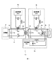
本発明の図1に示す第1の構成は、磁気パルス圧縮回路において、電圧分圧用の可飽和リアクトルSLbを負荷に対して並列接続することによって、未飽和の磁気スイッチを構成する可飽和リアクトルSLaに印加する電圧を大きくする構成に適用する構成であり、磁気パルス圧縮回路の磁気スイッチを構成する可飽和リアクトルSLa、および電圧分圧用の可飽和リアクトルSLbのそれぞれに対してリセット巻き線を施し、このリセット巻き線を介してリセット回路を接続する構成である。 First configuration shown in FIG. 1 of the present invention, the magnetic pulse compression circuit, by parallel connection of a saturable reactor SL b voltage voltage-dividing the load, the saturable reactor constituting a magnetic switch unsaturation a structure used in the configuration to increase the voltage applied to the SL a, saturable reactors SL a constituting the magnetic switch of the magnetic pulse compression circuit, and a reset winding for each of the saturable reactors SL b voltage voltage-dividing In this configuration, a reset circuit is connected via the reset winding.
[第1の構成例]
はじめに、本発明のパルス電源装置および磁気パルス圧縮回路の第1の構成例について説明する。図1は本発明のパルス電源装置および磁気パルス圧縮回路の第1の構成の概略を説明するための図であり、図2は図1に示す磁気パルス圧縮回路4aを等価的に表す図である。
[First configuration example]
First, a first configuration example of the pulse power supply device and the magnetic pulse compression circuit of the present invention will be described. FIG. 1 is a diagram for explaining an outline of a first configuration of a pulse power supply device and a magnetic pulse compression circuit according to the present invention, and FIG. 2 is an equivalent diagram of the magnetic
図1において、本発明のパルス電源装置1Aは、充電器2に接続されたパルス発生回路3と、パルス発生回路3で発生したパルスのパルス幅を圧縮し、圧縮した狭幅のパルス電流を負荷5に供給する磁気パルス圧縮回路4aと、リセット回路6a、6b、6cを備える。リセット回路6aは、パルス発生回路3の可飽和リアクトルSLPを飽和状態から不飽和状態にリセットし、リセット回路6bは、磁気パルス圧縮回路4aの可飽和リアクトルSLaを飽和状態から不飽和状態にリセットし、リセット回路6cは、磁気パルス圧縮回路4aの可飽和リアクトルSLbを飽和状態から不飽和状態にリセットする。
In FIG. 1, a pulse
図2は図1の磁気パルス圧縮回路4aを等価的に表した等価回路を示している。図2の等価回路において、可飽和リアクトルSLaの飽和前のインダクタンスをL11とし、可飽和リアクトルSLbの飽和前のインダクタンスをL21としている。
FIG. 2 shows an equivalent circuit equivalently representing the magnetic
可飽和リアクトルSLaには、磁気パルス圧縮回路4aの回路を構成する巻き線とリセット回路6bを構成する巻き線が施され、また、可飽和リアクトルSLbには磁気パルス圧縮回路4aの回路を構成する巻き線とリセット回路6cを構成する巻き線が施されているため、可飽和リアクトルの巻き線とリセット回路の巻き線との間でトランスアクションが行われる。
The saturable reactor SL a, winding constituting the winding and the
リセット回路6bのチョークコイルLcbのインダクタンスL101およびリセット回路6cのチョークコイルLccのインダクタンスL102は、磁気パルス圧縮回路4a側から見てそれぞれ換算インダクタンスL111(=L101・n1 2)、L112(=L102・n2 2)で表される。したがって、可飽和リアクトルSLaのインピーダンスは、可飽和リアクトルSLa自体のインピーダンスL11と換算インダクタンスL111との合成インピーダンスL1で表すことができ、可飽和リアクトルSLbのインピーダンスは、可飽和リアクトルSLb自体のインピーダンスL12と換算インダクタンスL112との合成インピーダンスL2で表すことができる。
The inductance L 101 of the choke coil L cb of the
パルス発生回路3は、充電器2に対して、可飽和リアクトルSLPとパルストランスPT1と半導体スイッチSWとを直列接続した回路と、コンデンサCPとを並列接続して構成される。コンデンサCPを充電器2によって初期充電した後、半導体スイッチSWをオン制御することによって、コンデンサCPからパルストランスPT1にパルス電流を供給する。可飽和リアクトルSLpは、半導体スイッチSWがオン動作した後に、不飽和状態から飽和状態とすることによって半導体スイッチSWのスイッチング損失を軽減する。
充電コンデンサC0はパルス発生回路3で発生させたパルス電流によって、パルストランスPT1を介して高圧充電される。この充電の間、可飽和リアクトルSLaは不飽和状態にある。可飽和リアクトルSLaは、充電コンデンサC0の充電電圧によって不飽和状態から飽和状態となることで磁気スイッチ動作し、磁気パルス圧縮した狭幅のパルス電圧を可飽和リアクトルSLbに発生させる。
The charging capacitor C 0 is charged with high voltage via the pulse transformer PT 1 by the pulse current generated by the
可飽和リアクトルとして繰り返して使用するには、次回の磁気スイッチ動作時までの電圧時間積を大きくするためにリセット制御が必要となる。リセット制御は、磁気スイッチ動作の後、可飽和リアクトルのコアに逆励磁電流を流して磁気リセットを行う。 In order to use it repeatedly as a saturable reactor, reset control is required to increase the voltage-time product until the next magnetic switch operation. In the reset control, after the magnetic switch operation, a reverse excitation current is supplied to the core of the saturable reactor to perform magnetic reset.
図2において、可飽和リアクトルSLaの換算インダクタンスL111は、リセット回路6bのチョークコイルLcbのインダクタンスL101と可飽和リアクトルSLaのリセット巻き線とメイン巻き線の巻き数比n1を用いて、
L111=n1 2・L101
で表される。
2, in terms of inductance L 111 saturable reactors SL a uses the turn ratio n 1 of the reset winding and the main winding of the inductance L 101 and the saturable reactor SL a choke coil L cb of the
L 111 = n 1 2 · L 101
It is represented by
したがって、図2に示す可飽和リアクトルSLaの合成インダクタンスL1は、可飽和リアクトルSLaの飽和前のインピーダンスL11と可飽和リアクトルSLaの換算インダクタンスL111との並列回路接続から
L1=L11//L111
となる。
Thus, the combined inductance of the saturable reactor SL a shown in FIG. 2 L 1 is a saturable reactor SL L a parallel circuit connection of the saturation and the previous impedance L 11 and converted inductance L 111 saturable reactors SL a of a 1 = L 11 // L 111
It becomes.
また、図2に示す可飽和リアクトルSLbの換算インダクタンスL112は、リセット回路6cのチョークコイルLccのインダクタンスL102と可飽和リアクトルSLbのリセット巻き線とメイン巻き線の巻き数比n2を用いて、
L112=n2 2・L102
となる。
Also, in terms of inductance L 112 saturable reactors SL b shown in FIG. 2, the
L 112 = n 2 2 · L 102
It becomes.
したがって、図2に示す可飽和リアクトルSLbの合成インダクタンスL2は、可飽和リアクトルSLbの飽和前のインピーダンスL21と可飽和リアクトルSLbの換算インダクタンスL112との並列回路接続から
L2=L21//L112
となる。
Thus, the synthesis of the saturable reactor SL b shown in FIG. 2 the inductance L 2 is saturable reactors SL parallel b saturation before and impedance L 21 and converted inductance L 112 saturable reactors SL b circuit connection from L 2 = L 21 // L 112
It becomes.
ここで、可飽和リアクトルSLaと可飽和リアクトルSLbは、充電コンデンサC0の電圧Vcを分圧する。 Here, the saturable reactor SL a saturable reactor SL b may divide the voltage Vc of the charging capacitor C 0.
可飽和リアクトルSLaおよび可飽和リアクトルSLbが飽和していないとき、この分圧によって可飽和リアクトルSLaに印加する電圧VSLaは、
VSLa=(L1/(L1+L2))・VC
で表される。
When the saturable reactor SL a and the saturable reactor SL b is not saturated, the voltage V SLa applied to the saturable reactor SL a by this partial pressure,
V SLa = (L 1 / (L 1 + L 2 )) · V C
It is represented by
一方、可飽和リアクトルSLbに印加する電圧VSLbは、
VSLb=(L2/(L1+L2))・VC
で表される。
On the other hand, the voltage V SLb applied to the saturable reactor SL b is:
V SLb = (L 2 / (L 1 + L 2 )) · V C
It is represented by
ここで、磁気パルス圧縮回路でパルス圧縮するパルスの幅は飽和時のインダクタンスとコンデンサとの積の平方根に比例するため、パルス幅を圧縮するにはインダクタンスが小さいことが求められる。 Here, since the width of the pulse to be compressed by the magnetic pulse compression circuit is proportional to the square root of the product of the inductance at the time of saturation and the capacitor, it is required that the inductance is small in order to compress the pulse width.
一方、インダクタンスはコアの断面積と巻き数の二乗との積に比例する。また、可飽和リアクトルの磁気スイッチ特性はコアの特性による飽和時のインダクタンス値に依存する。すなわち、磁気スイッチが必要とする電圧・時間積を満たすと共にインダクタンスLを小さくするには、巻き数を減らすと共に断面積を増やす必要がある。この断面積を増すと、可飽和リアクトルのサイズが大きくなるという問題が生じる。 On the other hand, the inductance is proportional to the product of the cross-sectional area of the core and the square of the number of turns. Further, the magnetic switch characteristic of the saturable reactor depends on the inductance value at the time of saturation due to the characteristic of the core. That is, in order to satisfy the voltage / time product required by the magnetic switch and reduce the inductance L, it is necessary to reduce the number of turns and increase the cross-sectional area. When this cross-sectional area is increased, there arises a problem that the size of the saturable reactor increases.
また、可飽和リアクトルSLaおよび可飽和リアクトルSLbにおいて、磁気パルス圧縮を行うには、これらの飽和前のインダクタンスL1とL2との間において、可飽和リアクトルSLaの合成インピーダンスL1と可飽和リアクトルSLbの合成インピーダンスL2とは、
L1≫L2
の関係となるように選定する必要がある。
In order to perform magnetic pulse compression in the saturable reactor SL a and the saturable reactor SL b , the combined impedance L 1 of the saturable reactor SL a and the inductance L 1 and L 2 before saturation the combined impedance L 2 of the saturable reactors SL b,
L 1 >> L 2
It is necessary to select so that
さらに可飽和リアクトルSLaが飽和した後のインダクタンスをL12とすると、負荷へパルスパワーを効率よく供給できるためには、飽和後のインピーダンスL12と合成インピーダンスL2とは、
L12≪L2
の関係となるように選定する必要がある。
Further saturable reactor SL a is the L 12 inductance after saturation, in order to be able to efficiently supply the pulse power to the load, the impedance L 12 after saturation with synthetic impedance L 2,
L 12 << L 2
It is necessary to select so that
このとき、L2=L21//L112の関係から、チョークコイルLccの可飽和リアクトルSLbへの換算インダクタンスL112を有効に利用して、可飽和リアクトルSLbの合成インダクタンスL2を、要求された値に選定することができる。 At this time, from the relationship of L 2 = L 21 // L 112 , the combined inductance L 2 of the saturable reactor SL b is obtained by effectively using the converted inductance L 112 to the saturable reactor SL b of the choke coil L cc. The required value can be selected.
また、L1=L11//L111の関係から、L1≫L2の関係を満たす可飽和リアクトルSLaの合成インピーダンスL1についても可飽和リアクトルSLbの換算インダクタンスL112を選定することによって小さくすることができる。 Further, L 1 = the relation L 11 // L 111, also selects the converted inductance L 112 saturable reactors SL b for the combined impedance L 1 saturable reactors SL a satisfies the relationship L 1 »L 2 Can be made smaller.
したがって、磁気スイッチを構成する可飽和リアクトルと電圧分圧用の可飽和リアクトルの分圧比は、電圧分圧用の可飽和リアクトルに接続されるリセット回路のチョークコイルのインダクタンスによって定めることができる。 Therefore, the voltage division ratio between the saturable reactor constituting the magnetic switch and the saturable reactor for voltage division can be determined by the inductance of the choke coil of the reset circuit connected to the saturable reactor for voltage division.
図2に示すパルス圧縮回路の等価回路4a´において、合成インピーダンスL1と合成インピーダンスL2との間の必要条件はL1≫L2である。
In the
このL1≫L2の条件は、任意の係数kを用いてL1=kL2によって選定することでき、L1=L11//L111とL2=L21//L112の関係を用いて、L11//L111=k(L21//L112)とすることができる。 The condition of L 1 >> L 2 can be selected by L 1 = kL 2 using an arbitrary coefficient k, and the relationship between L 1 = L 11 // L 111 and L 2 = L 21 // L 112 is obtained. It is possible to use L 11 // L 111 = k (L 21 // L 112 ).
ここで、例えばリセット回路6cにおける可飽和インピーダンスLccのインダクタンスL102を有効に利用し、合成インピーダンスL2を磁気パルス圧縮回路側から見た換算インダクタンスL112に依存させて選定した場合、合成インダクタンスL2は換算インダクタンスL112がない場合と比較して小さなインダクタンスとすることができる。
Here, for example, when effectively utilizing the inductance L 102 of the saturable impedance L cc in the
したがってL1=kL2を満たすL1=L11//L111のインダクタンス値を小さくすることができ、ここでL11のインダクタンスを小さくする。 Therefore, the inductance value of L 1 = L 11 // L 111 that satisfies L 1 = kL 2 can be reduced, and the inductance of L 11 is reduced here.
したがって、リセット回路6cのチョークコイルL102を利用することによって、可飽和リアクトルを小型化することができる。
Thus, by utilizing the choke coil L 102 of the
本発明の形態によれば、可飽和リアクトルSLaのインダクタンスを小さくすることによって、可飽和リアクトルのサイズを小型化し、可飽和リアクトルを形成するコアの量を低減させてコストを低減させることができる。 According to the embodiment of the present invention, by reducing the inductance of the saturable reactor SL a, to reduce the size of the saturable reactor, you are possible to reduce the cost by reducing the amount of core forming the saturable reactor .
また、本発明の形態によれば、リセット回路側のチョークコイルのインダクタンスによって電圧分圧を調整することができ、リセット回路側は磁気パルス圧縮回路側よりも低電圧であるため、低電圧において分圧調整が可能となるため、絶縁処理が容易となり、コストを低減させることができる。 Further, according to the embodiment of the present invention, the voltage division can be adjusted by the inductance of the choke coil on the reset circuit side, and the reset circuit side has a lower voltage than the magnetic pulse compression circuit side. Since pressure adjustment is possible, insulation processing is facilitated and costs can be reduced.
[第2の構成例]
次に、本発明のパルス電源装置および磁気パルス圧縮回路の第2の構成例について説明する。図3に示す第2の構成は、前記した第1の構成の電圧分圧用の可飽和リアクトルSLbに代えてパルストランスPT2を備える構成である。
[Second configuration example]
Next, a second configuration example of the pulse power supply device and the magnetic pulse compression circuit of the present invention will be described. The second configuration shown in Figure 3 is configured to include a pulse transformer PT 2 in place of the saturable reactor SL b voltage voltage-dividing the first configuration described above.
次に、本発明のパルス電源装置および磁気パルス圧縮回路の第2の構成例について説明する。図3は本発明のパルス電源装置および磁気パルス圧縮回路の第2の構成の概略を説明するための図であり、図4は図3の磁気パルス圧縮回路4bを等価的に表す図である。
Next, a second configuration example of the pulse power supply device and the magnetic pulse compression circuit of the present invention will be described. FIG. 3 is a diagram for explaining the outline of the second configuration of the pulse power supply device and the magnetic pulse compression circuit of the present invention, and FIG. 4 is an equivalent diagram of the magnetic
図3において、本発明のパルス電源装置1Bは、充電器2に接続されたパルス発生回路3と、パルス発生回路3で発生したパルスのパルス幅を圧縮し、圧縮した狭幅のパルス電流を負荷5に供給する磁気パルス圧縮回路4bと、リセット回路6a、6b、6dを備える。リセット回路6aは、パルス発生回路3の可飽和リアクトルSLPを飽和状態から不飽和状態にリセットし、リセット回路6bは、磁気パルス圧縮回路4bの可飽和リアクトルSLaを飽和状態から不飽和状態にリセットし、リセット回路6dは、パルストランスPT2の可飽和リアクトルを飽和状態から不飽和状態にリセットする。
In FIG. 3, a pulse power supply device 1B of the present invention compresses a
図4は図3の磁気パルス圧縮回路4bを等価的に表した等価回路4b´を示している。図4の等価回路において、可飽和リアクトルSLa飽和前のインダクタンスをL11とし、パルストランスPT2の飽和前の相互インダクタンスをM1としている。
FIG. 4 shows an
可飽和リアクトルSLaには、磁気パルス圧縮回路4bの回路を構成する巻き線とリセット回路6bを構成する巻き線が施され、また、パルストランスPT2の可飽和リアクトルには磁気パルス圧縮回路4bの回路を構成する巻き線とリセット回路6dを構成する巻き線が施されているため、パルストランスの可飽和リアクトルの巻き線とリセット回路の巻き線との間でトランスアクションが行われる。
The saturable reactor SL a, winding constituting the winding and the
リセット回路6bのチョークコイルLcbのインダクタンスL101およびリセット回路6dのチョークコイルLcdのインダクタンスL103は、磁気パルス圧縮回路4b側から見てそれぞれ換算インダクタンスL111(=L101・n1 2)、L113(=L103・n3 2)で表される。したがって、可飽和リアクトルSLaのインピーダンスは、可飽和リアクトルSLa自体のインピーダンスL11と換算インダクタンスL111との合成インピーダンスL1で表すことができ、パルストランスPT2のインピーダンスは、パルストランスのPT2の相互インダクタンスM1と換算インダクタンスL113との合成インピーダンスL3で表すことができる。
The inductance L 101 of the choke coil L cb of the
第2の構成のパルストランスPT2を用いた構成においても、第1の構成と同様に選定できる。 The configuration using the pulse transformer PT2 of the second configuration can be selected similarly to the first configuration.
図4において、可飽和リアクトルSLaの換算インダクタンスL111は、リセット回路6bのチョークコイルLcbのインダクタンスL101と可飽和リアクトルSLaのリセット巻き線とメイン巻き線の巻き数比n1を用いて、
L111=n1 2・L101
で表される。
4, in terms of inductance L 111 saturable reactors SL a uses the turn ratio n 1 of the reset winding and the main winding of the inductance L 101 and the saturable reactor SL a choke coil L cb of the
L 111 = n 1 2 · L 101
It is represented by
したがって、図4に示す可飽和リアクトルSLaの合成インダクタンスL1は、可飽和リアクトルSLaの飽和前のインピーダンスL11と可飽和リアクトルSLaの換算インダクタンスL111との並列回路接続から
L1=L11//L111
となる。
Thus, the combined inductance of the saturable reactor SL a shown in FIG. 4 L 1 is a saturable reactor SL L a parallel circuit connection of the saturation and the previous impedance L 11 and converted inductance L 111 saturable reactors SL a of a 1 = L 11 // L 111
It becomes.
また、図4に示すパルストランスPT2の換算インダクタンスL113は、リセット回路6dのチョークコイルLcdのインダクタンスL103とパルストランスPT2のリセット巻き線とメイン巻き線の巻き数比n3を用いて、
L113=n3 2・L103
となる。
Further, the converted inductance L 113 of the pulse transformer PT 2 shown in FIG. 4 uses the inductance L 103 of the choke coil L cd of the
L 113 = n 3 2 · L 103
It becomes.
したがって、図4に示すパルストランスPT2の合成インダクタンスL3は、飽和前の相互インピーダンスM1とパルストランスPT2の換算インダクタンスL113との並列回路接続から
L3=M1//L113
となる。
Thus, the combined inductance L 3 of the pulse transformer PT 2 shown in FIG. 4, L 3 = M 1 a parallel circuit connection of the converted inductance L 113 of saturated previous mutual impedance M 1 and the pulse transformer PT 2 // L 113
It becomes.
ここで、可飽和リアクトルSLaとパルストランスPT2は、充電コンデンサC0の電圧Vcを分圧する。 Here, the saturable reactor SL a pulse transformer PT 2 is dividing the voltage Vc of the charging capacitor C 0.
可飽和リアクトルSLaおよびパルストランスPT2が飽和していないとき、この分圧によって可飽和リアクトルSLaに印加する電圧VSLaは、
VSLa=(L1/(L1+L3))・VC
で表される。
When the saturable reactor SL a and the pulse transformer PT 2 is not saturated, the voltage V SLa applied to the saturable reactor SL a by this partial pressure,
V SLa = (L 1 / (L 1 + L 3 )) · V C
It is represented by
一方、パルストランスPT2に印加する電圧VPT2は、
VPT2=(L3/(L1+L3))・VC
で表される。
On the other hand, the voltage V PT2 to be applied to the pulse transformer PT 2 is
V PT2 = (L 3 / (L 1 + L 3 )) · V C
It is represented by
また、可飽和リアクトルSLaおよびパルストランスPT2において、磁気パルス圧縮を行うには、これらの飽和前のインダクタンスL1とL3との間において、可飽和リアクトルSLaの合成インピーダンスL1とパルストランスPTの合成インピーダンスL3とは、
L1≫L3
の関係となるように選定する必要がある。
Further, the saturable reactor SL a and the pulse transformer PT 2, the performing magnetic pulse compression, between the inductance L 1 and L 3 before these saturated, the combined impedance L 1 and the pulse of the saturable reactor SL a the combined impedance L 3 of the transformer PT,
L 1 >> L 3
It is necessary to select so that
さらに可飽和リアクトルSLaが飽和した後のインダクタンスをL12とすると、負荷へパルスパワーを効率よく供給できるためには、飽和後のインピーダンスL12と合成インピーダンスL3とは、
L12≪L3
の関係となるように選定する必要がある。
Further saturable reactor SL a is the L 12 inductance after saturation, in order to be able to efficiently supply the pulse power to the load, the impedance L 12 after saturation with synthetic impedance L 3,
L 12 << L 3
It is necessary to select so that
このとき、L3=M1//L113の関係から、チョークコイルLcdのパルストランスPT2への換算インダクタンスL113を有効に利用して、パルストランスPT2の合成インダクタンスL3を要求された値に選定することができる。 At this time, from the relationship of L 3 = M 1 // L 113 , the combined inductance L 3 of the pulse transformer PT 2 is required by effectively using the converted inductance L 113 of the choke coil L cd to the pulse transformer PT 2 . Can be selected.
また、L1=L11//L111の関係から、L1≫L3の関係を満たす可飽和リアクトルSLaの合成インピーダンスL1についてもパルストランスPT2の換算インダクタンスL113を選定することによって小さくすることができる。 Further, from the relationship of L 1 = L 11 // L 111 , by also selecting a conversion inductance L 113 of the pulse transformer PT 2 for the combined impedance L 1 saturable reactors SL a satisfies the relationship L 1 »L 3 Can be small.
したがって、磁気スイッチを構成する可飽和リアクトルと電圧分圧用のパルストランスの分圧比は、電圧分圧用のパルストランスに接続されるリセット回路のチョークコイルのインダクタンスによって定めることができる。 Therefore, the voltage division ratio between the saturable reactor constituting the magnetic switch and the voltage dividing pulse transformer can be determined by the inductance of the choke coil of the reset circuit connected to the voltage dividing pulse transformer.
[動作例]
図5は図1および図3に示す構成例の信号図を表し、電圧V1、V2、V3、V4は図1および図3の電圧V1、V2、V3、V4に相当している。また、図6は不飽和状態での動作図(図6(a))、および飽和状態での動作図(図6(b))を示している。
[Example of operation]
FIG. 5 shows a signal diagram of the configuration example shown in FIGS. 1 and 3, and voltages V1, V2, V3, and V4 correspond to voltages V1, V2, V3, and V4 in FIGS. FIG. 6 shows an operation diagram in the unsaturated state (FIG. 6A) and an operation diagram in the saturated state (FIG. 6B).
図5の信号図中の区間A、および図6(a)の動作図は、磁気スイッチを構成する可飽和リアクトルSLaが不飽和状態を示している。 Section A in the signal diagram of FIG. 5 and FIG. 6 Operation Figure (a) is a saturable reactor SL a constituting the magnetic switch indicates an unsaturated state.
この可飽和リアクトルSLaが不飽和状態にあるときには、印加電圧は合成インピーダンスL1と合成インピーダンスL2によって分圧される。 When this saturable reactor SL a is in the unsaturated state, the applied voltage is divided by the combined impedance L 1 and the synthetic impedance L 2.
この不飽和状態では、合成インピーダンスL1と合成インピーダンスL2との間には、L1≫L2の条件により、可飽和リアクトルSLaに印加する電圧VSLaは可飽和リアクトルSLbに印加する電圧VSLbよりも大となる。図5(c)のV3と図5(d)のV4はこの関係を示している。 In this unsaturated state, the voltage V SLa applied to the saturable reactor SL a is applied to the saturable reactor SL b between the synthetic impedance L 1 and the synthetic impedance L 2 under the condition of L 1 >> L 2. It becomes larger than the voltage VSLb . V3 in FIG. 5C and V4 in FIG. 5D show this relationship.
図5の信号図中の区間B、および図6(b)の動作図は、磁気スイッチを構成する可飽和リアクトルSLaが飽和状態を示している。 Section B in the signal diagram of FIG. 5, and 6 operation diagram of (b) is a saturable reactor SL a constituting the magnetic switch indicates the saturation.
この可飽和リアクトルSLaが飽和状態にあるときには、可飽和リアクトルSLaはトランスアクションしないため、印加電圧は飽和後のインピーダンスL12と合成インピーダンスL2によって分圧される。 When the saturable reactor SL a is in the saturated state, the saturable reactor SL a because no transformer action, the applied voltage is divided by the combined impedance L 2 the impedance L 12 after saturation.
この飽和状態では、可飽和リアクトルのインピーダンスL12と合成インピーダンスL2との間には、L12≪L2の条件により、図5(d)の区間Bに示すように、可飽和リアクトルSLbに印加する電圧VSLbは急激に増大し、負荷にパルス電流が供給される。 In this saturation state, the saturable reactor SL b is placed between the saturable reactor impedance L 12 and the combined impedance L 2 as shown in section B of FIG. 5 (d) under the condition of L 12 << L 2 . The voltage V SLb applied to the voltage increases rapidly, and a pulse current is supplied to the load.
なお、本発明は前記各実施の形態に限定されるものではない。本発明の趣旨に基づいて種々変形することが可能であり、これらを本発明の範囲から排除するものではない。 The present invention is not limited to the embodiments described above. Various modifications can be made based on the spirit of the present invention, and these are not excluded from the scope of the present invention.
本発明のパルス電源装置および磁気パルス圧縮回路は、成膜装置に限らず、スパッタリング装置やアッシング装置等のプラズマを用いる処理装置分野に適用することができる。 The pulse power supply device and magnetic pulse compression circuit of the present invention can be applied not only to a film forming apparatus but also to a processing apparatus field using plasma such as a sputtering apparatus or an ashing apparatus.
1A,1B パルス電源装置
2 充電器
3 パルス発生回路
4a,4b 磁気パルス圧縮回路
4a´,4b´ 磁気パルス圧縮回路の等価回路
5 負荷
6a、6b、6c、6d リセット回路
1A, 1B Pulse
Claims (10)
前記磁気パルス圧縮回路の可飽和リアクトルを飽和状態から不飽和状態にリセットするリセット回路を備え、
前記リセット回路はリセット巻き線と直流電源間にチョークコイルを接続し、
前記磁気パルス圧縮回路の電圧分圧用の可飽和リアクトルの等価インダクタンスを、磁気パルス圧縮回路の可飽和リアクトルとリセット回路のチョークコイルとの並列合成インピーダンスにより設定し、当該並列合成インピーダンスを小さくすることによって、磁気パルス圧縮回路の磁気スイッチ側の可飽和リアクトルのインダクタンスを小さく設定することを特徴とする、磁気パルス圧縮回路。 A magnetic pulse compression circuit that compresses a current discharged from a charging capacitor by a magnetic switch operation of a saturable reactor and flows a pulse current,
A reset circuit for resetting the saturable reactor of the magnetic pulse compression circuit from a saturated state to an unsaturated state;
The reset circuit connects a choke coil between a reset winding and a DC power source,
By setting the equivalent inductance of the saturable reactor for voltage division of the magnetic pulse compression circuit by the parallel composite impedance of the saturable reactor of the magnetic pulse compression circuit and the choke coil of the reset circuit, and reducing the parallel composite impedance The magnetic pulse compression circuit is characterized in that the inductance of the saturable reactor on the magnetic switch side of the magnetic pulse compression circuit is set small.
前記磁気パルス圧縮回路の可飽和リアクトルを飽和状態から不飽和状態にリセットするリセット回路を備え、
前記リセット回路はリセット巻き線と直流電源間にチョークコイルを接続し、
前記磁気パルス圧縮回路は、前記充電コンデンサと負荷との間に直列接続する第1の可飽和リアクトルと、前記第1の可飽和リアクトルと負荷との間に負荷に対して並列接続する第2の可飽和リアクトルとを備え、
前記第2の可飽和リアクトルの等価インダクタンスを、磁気パルス圧縮回路の第2の可飽和リアクトルと第2のリセット回路のチョークコイルとの並列合成インピーダンスにより設定し、
第2の可飽和リアクトルと第2のリセット回路のチョークコイルとの並列合成インピーダンスを小さくすることによって、磁気パルス圧縮回路の磁気スイッチ側の可飽和リアクトルのインダクタンスを小さく設定することを特徴とする、磁気パルス圧縮回路。 A magnetic pulse compression circuit that compresses a current discharged from a charging capacitor by a magnetic switch operation of a saturable reactor and flows a pulse current,
A reset circuit for resetting the saturable reactor of the magnetic pulse compression circuit from a saturated state to an unsaturated state;
The reset circuit connects a choke coil between a reset winding and a DC power source,
The magnetic pulse compression circuit includes a first saturable reactor connected in series between the charging capacitor and the load, and a second connected in parallel to the load between the first saturable reactor and the load. With a saturable reactor,
The equivalent inductance of the second saturable reactor is set by a parallel combined impedance of the second saturable reactor of the magnetic pulse compression circuit and the choke coil of the second reset circuit,
The inductance of the saturable reactor on the magnetic switch side of the magnetic pulse compression circuit is set to be small by reducing the parallel combined impedance of the second saturable reactor and the choke coil of the second reset circuit. Magnetic pulse compression circuit.
前記磁気パルス圧縮回路の可飽和リアクトルを飽和状態から不飽和状態にリセットするリセット回路を備え、
前記リセット回路はリセット巻き線と直流電源間にチョークコイルを接続し、
前記磁気パルス圧縮回路は、前記充電コンデンサと負荷との間に直列接続する第1の可飽和リアクトルと、
前記第1の可飽和リアクトルと負荷との間に負荷に対して並列接続するパルストランスとを備え、
前記パルストランスの等価インダクタンスを、磁気パルス圧縮回路のパルストランスと第2のリセット回路のチョークコイルとの並列合成インピーダンスにより設定し、
磁気パルス圧縮回路のパルストランスと第2のリセット回路のチョークコイルとの並列合成インピーダンスを小さくすることによって、磁気パルス圧縮回路の磁気スイッチ側の可飽和リアクトルのインダクタンスを小さく設定することを特徴とする、磁気パルス圧縮回路。 A magnetic pulse compression circuit that compresses a current discharged from a charging capacitor by a magnetic switch operation of a saturable reactor and flows a pulse current,
A reset circuit for resetting the saturable reactor of the magnetic pulse compression circuit from a saturated state to an unsaturated state;
The reset circuit connects a choke coil between a reset winding and a DC power source,
The magnetic pulse compression circuit includes a first saturable reactor connected in series between the charging capacitor and a load;
A pulse transformer connected in parallel to the load between the first saturable reactor and the load;
The equivalent inductance of the pulse transformer is set by a parallel combined impedance of the pulse transformer of the magnetic pulse compression circuit and the choke coil of the second reset circuit,
The inductance of the saturable reactor on the magnetic switch side of the magnetic pulse compression circuit is set small by reducing the parallel combined impedance of the pulse transformer of the magnetic pulse compression circuit and the choke coil of the second reset circuit. Magnetic pulse compression circuit.
直流電源で充電される充電コンデンサと、
可飽和リアクトルの磁気スイッチ動作によって前記充電コンデンサから負荷に圧縮したパルス電流を流す磁気パルス圧縮回路と、
前記磁気パルス圧縮回路の可飽和リアクトルを飽和状態から不飽和状態にリセットするリセット回路とを備え、
前記リセット回路はリセット巻き線と直流電源間にチョークコイルを接続し、
前記磁気パルス圧縮回路の電圧分圧用の可飽和リアクトルの等価インダクタンスを、磁気パルス圧縮回路の可飽和リアクトルとリセット回路のチョークコイルとの並列合成インピーダンスにより設定し、当該並列合成インピーダンスを小さくすることによって、磁気パルス圧縮回路の磁気スイッチ側の可飽和リアクトルのインダクタンスを小さく設定することを特徴とする、パルス電源装置。 A pulse power supply device that supplies a pulse of high voltage and narrow current width to a load,
A charging capacitor charged with a DC power supply;
A magnetic pulse compression circuit for supplying a pulse current compressed from the charging capacitor to a load by a magnetic switch operation of a saturable reactor;
A reset circuit for resetting the saturable reactor of the magnetic pulse compression circuit from a saturated state to an unsaturated state;
The reset circuit connects a choke coil between a reset winding and a DC power source,
By setting the equivalent inductance of the saturable reactor for voltage division of the magnetic pulse compression circuit by the parallel composite impedance of the saturable reactor of the magnetic pulse compression circuit and the choke coil of the reset circuit, and reducing the parallel composite impedance A pulse power supply device, wherein the inductance of the saturable reactor on the magnetic switch side of the magnetic pulse compression circuit is set small.
直流電源で充電される充電コンデンサと、
可飽和リアクトルの磁気スイッチ動作によって前記充電コンデンサから負荷に圧縮したパルス電流を流す磁気パルス圧縮回路と、
前記磁気パルス圧縮回路の可飽和リアクトルを飽和状態から不飽和状態にリセットするリセット回路とを備え、
前記リセット回路はリセット巻き線と直流電源間にチョークコイルを接続し、
前記磁気パルス圧縮回路は、前記充電コンデンサと負荷との間に直列接続する第1の可飽和リアクトルと、
前記第1の可飽和リアクトルと負荷との間に負荷に対して並列接続する第2の可飽和リアクトルとを備え、
前記第2の可飽和リアクトルの等価インダクタンスを、磁気パルス圧縮回路の第2の可飽和リアクトルと第2のリセット回路のチョークコイルとの並列合成インピーダンスにより設定し、
第2の可飽和リアクトルと第2のリセット回路のチョークコイルとの並列合成インピーダンスを小さくすることによって、磁気パルス圧縮回路の磁気スイッチ側の可飽和リアクトルのインダクタンスを小さく設定することを特徴とする、パルス電源装置。 A pulse power supply device that supplies a pulse of high voltage and narrow current width to a load,
A charging capacitor charged with a DC power supply;
A magnetic pulse compression circuit for supplying a pulse current compressed from the charging capacitor to a load by a magnetic switch operation of a saturable reactor;
A reset circuit for resetting the saturable reactor of the magnetic pulse compression circuit from a saturated state to an unsaturated state;
The reset circuit connects a choke coil between a reset winding and a DC power source,
The magnetic pulse compression circuit includes a first saturable reactor connected in series between the charging capacitor and a load;
A second saturable reactor connected in parallel with the load between the first saturable reactor and the load;
The equivalent inductance of the second saturable reactor is set by a parallel combined impedance of the second saturable reactor of the magnetic pulse compression circuit and the choke coil of the second reset circuit,
The inductance of the saturable reactor on the magnetic switch side of the magnetic pulse compression circuit is set to be small by reducing the parallel combined impedance of the second saturable reactor and the choke coil of the second reset circuit. Pulse power supply.
直流電源で充電される充電コンデンサと、
可飽和リアクトルの磁気スイッチ動作によって前記充電コンデンサから負荷に圧縮したパルス電流を流す磁気パルス圧縮回路と、
前記磁気パルス圧縮回路の可飽和リアクトルを飽和状態から不飽和状態にリセットするリセット回路とを備え、
前記リセット回路はリセット巻き線と直流電源間にチョークコイルを接続し、
前記磁気パルス圧縮回路は、前記充電コンデンサと負荷との間に直列接続する第1の可飽和リアクトルと、
前記第1の可飽和リアクトルと負荷との間に負荷に対して並列接続するパルストランスとを備え、
前記パルストランスの等価インダクタンスを、磁気パルス圧縮回路のパルストランスと第2のリセット回路のチョークコイルとの並列合成インピーダンスにより設定し、
磁気パルス圧縮回路のパルストランスと第2のリセット回路のチョークコイルとの並列合成インピーダンスを小さくすることによって、磁気パルス圧縮回路の磁気スイッチ側の可飽和リアクトルのインダクタンスを小さく設定することを特徴とする、磁気パルス電源装置。 A pulse power supply device that supplies a pulse of high voltage and narrow current width to a load,
A charging capacitor charged with a DC power supply;
A magnetic pulse compression circuit for supplying a pulse current compressed from the charging capacitor to a load by a magnetic switch operation of a saturable reactor;
A reset circuit for resetting the saturable reactor of the magnetic pulse compression circuit from a saturated state to an unsaturated state;
The reset circuit connects a choke coil between a reset winding and a DC power source,
The magnetic pulse compression circuit includes a first saturable reactor connected in series between the charging capacitor and a load;
A pulse transformer connected in parallel to the load between the first saturable reactor and the load;
The equivalent inductance of the pulse transformer is set by a parallel combined impedance of the pulse transformer of the magnetic pulse compression circuit and the choke coil of the second reset circuit,
The inductance of the saturable reactor on the magnetic switch side of the magnetic pulse compression circuit is set small by reducing the parallel combined impedance of the pulse transformer of the magnetic pulse compression circuit and the choke coil of the second reset circuit. Magnetic pulse power supply device.
Priority Applications (1)
| Application Number | Priority Date | Filing Date | Title |
|---|---|---|---|
| JP2009041018A JP5270399B2 (en) | 2009-02-24 | 2009-02-24 | Magnetic pulse compression circuit and pulse power supply device |
Applications Claiming Priority (1)
| Application Number | Priority Date | Filing Date | Title |
|---|---|---|---|
| JP2009041018A JP5270399B2 (en) | 2009-02-24 | 2009-02-24 | Magnetic pulse compression circuit and pulse power supply device |
Publications (3)
| Publication Number | Publication Date |
|---|---|
| JP2010200446A JP2010200446A (en) | 2010-09-09 |
| JP2010200446A5 JP2010200446A5 (en) | 2012-03-01 |
| JP5270399B2 true JP5270399B2 (en) | 2013-08-21 |
Family
ID=42824569
Family Applications (1)
| Application Number | Title | Priority Date | Filing Date |
|---|---|---|---|
| JP2009041018A Expired - Fee Related JP5270399B2 (en) | 2009-02-24 | 2009-02-24 | Magnetic pulse compression circuit and pulse power supply device |
Country Status (1)
| Country | Link |
|---|---|
| JP (1) | JP5270399B2 (en) |
Cited By (2)
| Publication number | Priority date | Publication date | Assignee | Title |
|---|---|---|---|---|
| EP3955447A4 (en) * | 2019-04-11 | 2023-04-26 | Kyosan Electric Mfg. Co., Ltd. | Pulsed dc power source device and duty control method for pulsed dc power source device |
| EP3955446A4 (en) * | 2019-04-11 | 2023-05-03 | Kyosan Electric Mfg. Co., Ltd. | Pulsed dc power source device and magnetic saturation reset method for pulsed dc power source device |
Families Citing this family (7)
| Publication number | Priority date | Publication date | Assignee | Title |
|---|---|---|---|---|
| CN103166613B (en) * | 2013-01-29 | 2015-12-09 | 华中科技大学 | A kind of Low-delay dispersive magnetic switch compression pulse power reset circuit |
| JP5771261B2 (en) | 2013-12-03 | 2015-08-26 | 株式会社Ifg | Medical continuous magnetic pulse generator |
| KR101615458B1 (en) | 2014-12-30 | 2016-04-26 | 주식회사 포스코아이씨티 | Apparatus for Resetting Magnetic of Magnetic Switch, System for Compressing High Voltage Pulse including That Apparatus, and Method for Controlling That System |
| JP6727436B2 (en) * | 2017-06-13 | 2020-07-22 | 三菱電機株式会社 | Pulse power supply |
| GB2584731B (en) * | 2019-06-13 | 2024-01-31 | Bae Systems Plc | Pulse charging of a capacitor |
| CN114035647B (en) * | 2021-11-23 | 2022-10-11 | 哈尔滨工业大学 | Pulse power device for generating disturbance magnetic field |
| WO2023166570A1 (en) * | 2022-03-01 | 2023-09-07 | ギガフォトン株式会社 | Gas laser device and method for manufacturing electronic device |
Family Cites Families (9)
| Publication number | Priority date | Publication date | Assignee | Title |
|---|---|---|---|---|
| JP2820722B2 (en) * | 1989-06-29 | 1998-11-05 | 日立金属株式会社 | High voltage pulse generation circuit, discharge pumped laser and accelerator using the same |
| JPH03124273A (en) * | 1989-10-03 | 1991-05-27 | Toshiba Corp | Pulse power source device |
| JPH03177086A (en) * | 1989-12-06 | 1991-08-01 | Hitachi Ltd | Pulse power supply device |
| JP3324203B2 (en) * | 1993-06-15 | 2002-09-17 | 株式会社明電舎 | Reset control circuit for multiple saturable reactors |
| JP3605896B2 (en) * | 1995-09-08 | 2004-12-22 | 株式会社明電舎 | Pulse power supply |
| JPH11332258A (en) * | 1998-05-08 | 1999-11-30 | Meidensha Corp | Pulse power supply |
| JP2004350338A (en) * | 2003-05-20 | 2004-12-09 | Meidensha Corp | Pulse power supply |
| JP2007104797A (en) * | 2005-10-04 | 2007-04-19 | Meidensha Corp | Pulse power supply device |
| JP4702156B2 (en) * | 2006-04-17 | 2011-06-15 | 株式会社明電舎 | Pulse power supply |
-
2009
- 2009-02-24 JP JP2009041018A patent/JP5270399B2/en not_active Expired - Fee Related
Cited By (4)
| Publication number | Priority date | Publication date | Assignee | Title |
|---|---|---|---|---|
| EP3955447A4 (en) * | 2019-04-11 | 2023-04-26 | Kyosan Electric Mfg. Co., Ltd. | Pulsed dc power source device and duty control method for pulsed dc power source device |
| EP3955446A4 (en) * | 2019-04-11 | 2023-05-03 | Kyosan Electric Mfg. Co., Ltd. | Pulsed dc power source device and magnetic saturation reset method for pulsed dc power source device |
| US11677385B2 (en) | 2019-04-11 | 2023-06-13 | Kyosan Electric Mfg. Co., Ltd. | DC pulse power supply device and duty control method for DC pulse power supply device |
| US11929668B2 (en) | 2019-04-11 | 2024-03-12 | Kyosan Electric Mfg. Co., Ltd. | DC pulse power supply device and magnetic saturation reset method for DC pulse power supply device |
Also Published As
| Publication number | Publication date |
|---|---|
| JP2010200446A (en) | 2010-09-09 |
Similar Documents
| Publication | Publication Date | Title |
|---|---|---|
| JP5270399B2 (en) | Magnetic pulse compression circuit and pulse power supply device | |
| JP4434048B2 (en) | DC / DC converter | |
| JP4692154B2 (en) | DC / DC converter | |
| US4618919A (en) | Topology for miniature power supply with low voltage and low ripple requirements | |
| US7768807B2 (en) | Bidirectional no load control with overshoot protection | |
| JP4434049B2 (en) | DC / DC converter | |
| CN102082512A (en) | Driver for piezoelectric actuator | |
| TW200535876A (en) | DC transformer with output inductor integrated on the magnetic core thereof and a DC/DC converter employing the same | |
| US5514918A (en) | Pulse generator | |
| JP4995640B2 (en) | Boost chopper device | |
| JP3693061B1 (en) | Switching power supply | |
| JP2008306786A5 (en) | ||
| WO2014054787A1 (en) | Converter and bi-directional converter | |
| TW201622324A (en) | DC-DC flyback converter for recycling leakage energy | |
| KR102571734B1 (en) | DC-DC converter | |
| JP4692155B2 (en) | Switching power supply | |
| JP5441418B2 (en) | Forward converter | |
| JP2005295654A (en) | Pulse power unit | |
| KR101229265B1 (en) | Integrated transformer and high step-up dc/dc converter using the same | |
| JPH07245549A (en) | High voltage pulse generator | |
| JP2011061953A (en) | Multi-output switching power supply device | |
| JP2971618B2 (en) | Pulse transformer and high voltage pulse generator | |
| JPWO2010082557A1 (en) | DC / DC converter and composite magnetic circuit | |
| CN110556242B (en) | On-load voltage regulating transformer and voltage regulating method | |
| JP2007104797A (en) | Pulse power supply device |
Legal Events
| Date | Code | Title | Description |
|---|---|---|---|
| A521 | Written amendment |
Free format text: JAPANESE INTERMEDIATE CODE: A523 Effective date: 20120116 |
|
| A621 | Written request for application examination |
Free format text: JAPANESE INTERMEDIATE CODE: A621 Effective date: 20120116 |
|
| A977 | Report on retrieval |
Free format text: JAPANESE INTERMEDIATE CODE: A971007 Effective date: 20130417 |
|
| TRDD | Decision of grant or rejection written | ||
| A01 | Written decision to grant a patent or to grant a registration (utility model) |
Free format text: JAPANESE INTERMEDIATE CODE: A01 Effective date: 20130507 |
|
| A61 | First payment of annual fees (during grant procedure) |
Free format text: JAPANESE INTERMEDIATE CODE: A61 Effective date: 20130509 |
|
| R150 | Certificate of patent or registration of utility model |
Free format text: JAPANESE INTERMEDIATE CODE: R150 |
|
| LAPS | Cancellation because of no payment of annual fees |