JP5259473B2 - Contact connector - Google Patents
Contact connector Download PDFInfo
- Publication number
- JP5259473B2 JP5259473B2 JP2009084075A JP2009084075A JP5259473B2 JP 5259473 B2 JP5259473 B2 JP 5259473B2 JP 2009084075 A JP2009084075 A JP 2009084075A JP 2009084075 A JP2009084075 A JP 2009084075A JP 5259473 B2 JP5259473 B2 JP 5259473B2
- Authority
- JP
- Japan
- Prior art keywords
- contact
- coil spring
- coil
- holding
- spring contact
- Prior art date
- Legal status (The legal status is an assumption and is not a legal conclusion. Google has not performed a legal analysis and makes no representation as to the accuracy of the status listed.)
- Expired - Fee Related
Links
Images


Landscapes
- Testing Of Individual Semiconductor Devices (AREA)
Description
本発明は、2つのユニットや回路基板の間に介在し、両者のそれぞれが有する複数の接続電極を互いに電気的に接続するコンタクトを備えたコンタクトコネクタに係り、特に、コンタクトに、コイルばねを用いたコンタクトコネクタに関する。 The present invention relates to a contact connector having a contact interposed between two units and a circuit board and electrically connecting a plurality of connection electrodes of each of the two units and a circuit board, and in particular, a coil spring is used for the contact. Related to contact connectors.
従来、接続電極を有する2つのユニットや回路基板の間に介在し、互いの接続電極を導通させて電気的に接続するコンタクト(接点)を備えたコンタクトコネクタが知られている。この種のコンタクトコネクタでは、ピン状のコンタクトが広く用いられており、また、このコンタクトとしてコイルばねを用いたものも知られている。
コイルばねを用いたコンタクトとしては、芯材たる絶縁体丸棒の周りに弾性金属線を螺旋状に巻いた構成(例えば、特許文献1)や、コイルばねの一部の巻き回し箇所(コイル)を一方の接続電極側に突出するように偏倚させた状態で該コイルばねを軸方向に押し縮めて固定した構成(例えば、特許文献2)が知られている。そして、これらコイルばねを用いたコンタクトによれば、ピン状のコンタクトに比べて接続電極の間の導伝路長を短縮可能となり、ユニットや回路基板を高速動作させた場合でも、接続電極間での信号遅延や信号歪みを抑制することができる。
As a contact using a coil spring, a structure in which an elastic metal wire is spirally wound around an insulator round bar as a core member (for example, Patent Document 1), or a part of a coil spring that is wound (coil) There is known a configuration (for example, Patent Document 2) in which the coil spring is axially pressed and contracted in a state in which the coil spring is biased so as to protrude toward one connection electrode. According to the contacts using these coil springs, the length of the conductive path between the connection electrodes can be shortened compared to the pin-shaped contact, and even when the unit or the circuit board is operated at high speed, the connection between the connection electrodes can be reduced. Signal delay and signal distortion can be suppressed.
しかしながら、特許文献1に記載の技術では、コイルばねの径方向の変形量が絶縁体丸棒によって規制されてしまう、という問題がある。さらに、ワークと接触した際に絶縁体丸棒に荷重がかかり撓むおそれがあり、ワークに対して均一な接触が確保できない可能性がある。また特許文献2の技術においても、径方向への偏倚部分を有するため、ワークに対して均一な接触が確保できない。
However, the technique described in
本発明は、上述した事情に鑑みてなされたものであり、コイルばねコンタクトの高密度配置を可能としつつ、ワークに対して均一な接触を確保可能なコンタクトコネクタを提供することを目的とする。 The present invention has been made in view of the above-described circumstances, and an object of the present invention is to provide a contact connector that can ensure uniform contact with a workpiece while enabling high-density arrangement of coil spring contacts.
上記目的を達成するために、本発明は、一対の接触電極の間に挟まれて各接触電極を導通する、側面視においてコイルの開始端が前段のコイルの幅内に位置するように金属線を巻き回して構成した複数のコイルばねコンタクトと、前記コイルばねコンタクトの径よりも幅が狭い幅狭部を少なくとも一部に有する複数の保持開口が形成され、前記保持開口のそれぞれに前記コイルばねコンタクトを該コイルばねコンタクトの外周部を一部突出させて前記幅狭部で保持する保持カバーと、底面に前記接触電極が形成された凹部に複数の前記コイルばねコンタクトが収められ、前記保持カバーで覆われたブロックと、を備え、前記保持カバーに保持されたコイルばねコンタクトの各々は、隣り合うコイルばねコンタクト間で前記コイルの倒れる向きを互いに反対にされ、前記コイルばねコンタクトの各々が前記ブロックと検査対象の接触電極の間に挟まれたときに、各コイルばねコンタクトにおけるコイルのそれぞれが軸方向の同じ向きに倒れるように弾性変形することを特徴とするコンタクトコネクタを提供する。 In order to achieve the above object, the present invention provides a metal wire that is sandwiched between a pair of contact electrodes and conducts each contact electrode so that the starting end of the coil is located within the width of the preceding coil in a side view. And a plurality of holding openings each having at least a portion of a narrow portion narrower than the diameter of the coil spring contact, and each of the holding openings is provided with a coil spring contact. A holding cover for holding the contact by the narrow portion with a part of the outer periphery of the coil spring contact projecting, and a plurality of the coil spring contacts in a recess having the contact electrode formed on the bottom surface, the holding cover and a block which is covered with, each coil spring contact which is held by the holding cover, the direction of fall of said coil between adjacent spring contacts Are opposite to each other, when each of the coil spring contacts is sandwiched between the contact electrodes to be inspected and the block, each of the coils in the coil spring contact is elastically deformed to fall in the same direction in the axial direction A contact connector is provided.
本発明によれば、一対の接触電極により挟まれて外周部が押圧されたときには、コイルばねコンタクトの各コイルが軸方向の同じ向きに倒れるように弾性変形するため、幅方向(径方向)への変形が抑制される。これにより、コイルばねコンタクト同士の干渉が防止されるため高密度化が可能となる。
さらに、かかるコイルばねコンタクトが保持カバーの保持開口の幅狭部で保持されているため、コイルばねコンタクトの弾性変形が保持部材により規制されることがなく、また、特許文献1に記載の絶縁体丸棒のような接触電極との接触時の荷重を受けて撓みが生じるような部材が不要となるから、ワークに対して均一な接触を確保可能することができる。
According to the present invention, when the outer peripheral portion is pressed between the pair of contact electrodes, each coil of the coil spring contact is elastically deformed so as to fall in the same axial direction. Is prevented from being deformed. Thereby, since interference between coil spring contacts is prevented, high density can be achieved.
Further, since the coil spring contact is held by the narrow portion of the holding opening of the holding cover, the elastic deformation of the coil spring contact is not restricted by the holding member, and the insulator described in
上記発明において、隣り合うコイルばねコンタクト間で前記コイルの倒れる向きを互いに反対にすることで、接触電極で挟まれたときに隣り合うコイルばねコンタクト同士が接触したとしても絡まりが発生することがないため、絡まりにより各コイルの倒れが規制されることがなく、接触電極へのあたりが強くなることが防止される。
In the invention, by reversing the direction of fall of said coil between adjacent coil spring contacts each other, is not generated entangled as a coil spring contacts adjacent when sandwiched between the contact electrode is in contact Therefore, the coil does not fall down due to the entanglement, and the contact with the contact electrode is prevented from becoming strong.
上記発明において、前記保持カバーの保持開口の端部に前記幅狭部を形成しても良い。
これによれば、コイルばねコンタクトの端部のコイルと保持開口の端部の幅狭部の間に隙間が設けられるため、接触電極時との接触時のコイルの倒れのストロークを大きくすることができる。また、コイルばねコンタクトの端部のコイルの外周部が幅狭部に係合することで、該コイルの逆方向への倒れが規制され、これにより、該コイルにより接触電極のあたりが強くなるのを防止できる。
In the above invention, the narrow portion may be formed at an end portion of the holding opening of the holding cover.
According to this, since a gap is provided between the coil at the end of the coil spring contact and the narrow portion at the end of the holding opening, the stroke of the coil collapse at the time of contact with the contact electrode can be increased. it can. In addition, the outer peripheral portion of the coil at the end of the coil spring contact is engaged with the narrow portion, so that the coil is prevented from falling in the reverse direction, and thereby the contact of the contact electrode is strengthened by the coil. Can be prevented.
また上記発明において、前記コイルばねコンタクトの端部のコイルの前記軸方向の移動を規制し、前記保持開口から突出した外周部の前記コイルの倒れを制限する規制部材を備えても良い。
こうすることで、規制部材により、保持開口から突出した外周部の前記コイルの倒れが制限され、コイルばねコンタクトが保持カバーの保持開口内部へ潜り込むことが防止される。
Moreover, in the said invention, you may provide the control member which controls the movement of the said axial direction coil of the edge part of the said coil spring contact, and restrict | limits the fall of the said coil of the outer peripheral part protruded from the said holding | maintenance opening.
By doing so, the regulation member limits the fall of the coil at the outer peripheral portion protruding from the holding opening, and prevents the coil spring contact from entering the holding opening of the holding cover.
本発明によれば、一対の接触電極により挟まれたときに、コイルばねコンタクトの各コイルが軸方向の同じ向きに倒れるように弾性変形して幅方向への変形が抑制されるため、コイルばねコンタクト同士の干渉が防止され高密度化が可能となる。また、カバーの保持開口の幅狭部でコイルばねコンタクトを保持するため、該コイルばねコンタクトの変形が規制されることがなく、ワークに対する均一な接触が確保できる。
上記発明において、隣り合うコイルばねコンタクト間で前記コイルの倒れる向きを互いに反対にすることで、隣り合うコイルばねコンタクト同士の絡まりを防止し、絡まりにより各コイルの倒れが規制されてしまうことを防止できる。
上記発明において、カバーの保持開口の端部に幅狭部を形成してコイルばねコンタクトの端部を保持することで、コイルばねコンタクトの端部のコイルの倒れのストロークを大きくすることができる。
上記発明において、コイルばねコンタクトの端部の軸方向の移動を規制してコイルの倒れを制限する規制部材を設けることで、コイルばねコンタクトの保持開口内部への潜り込みを防止することができる。
According to the present invention, when sandwiched between a pair of contact electrodes, each coil of the coil spring contact is elastically deformed so as to fall in the same direction in the axial direction and the deformation in the width direction is suppressed. Interference between contacts is prevented and high density is possible. Further, since the coil spring contact is held by the narrow portion of the holding opening of the cover, deformation of the coil spring contact is not restricted, and uniform contact with the work can be ensured.
In the above invention, by making the direction in which the coils fall between adjacent coil spring contacts opposite to each other, the coil spring contacts adjacent to each other are prevented from being entangled, and the entanglement prevents each coil from falling. it can.
In the above invention, by forming a narrow portion at the end of the holding opening of the cover and holding the end of the coil spring contact, the stroke of the coil collapse at the end of the coil spring contact can be increased.
In the above invention, by providing a restricting member that restricts the axial movement of the end portion of the coil spring contact and restricts the collapse of the coil, the coil spring contact can be prevented from entering the holding opening.
<第1実施形態>
以下、図面を参照して本発明の実施形態について説明する。以下では、パワーデバイス用のプラスチックモジュール、特に、電鉄、車両用のIGBT(Insulated Gate Bipolar Transistor)モジュールをパッケージ化する前にIGBTに電流を供給して動作検査するための装置に本発明を適用した場合を例示する。
<First Embodiment>
Hereinafter, embodiments of the present invention will be described with reference to the drawings. In the following, the present invention is applied to an apparatus for supplying current to an IGBT and inspecting its operation before packaging a plastic module for a power device, in particular, an electric railway and an IGBT (Insulated Gate Bipolar Transistor) module for a vehicle. The case is illustrated.
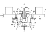
図1は、本実施形態に係る検査装置1の構成を模式的に示す図である。この検査装置1は、パッケージ化する前のIGBTモジュールのIGBT3に対するRBSOA(逆バイアス安全動作領域)耐量試験をする装置である。
IGBT3は、図2に示すように、その上面に、ゲート電極4及びゲート電極4に絶縁分離された互いに同一電位を有する5つのエミッタ電極6と1つのエミッタセンス電極8が上面に形成され、裏面にコレクタ電極(図示せず)が形成された半導体デバイスである。
そして検査装置1は、IGBT3のコレクタ・エミッタ間に例えば約1000Vの高電圧を印加して約340Aの大電流を通電することで、RBSOA耐量試験を可能にする。
FIG. 1 is a diagram schematically showing a configuration of an
As shown in FIG. 2, the
Then, the
検査装置1について詳細には、図1に示すように、検査装置1は、IGBT3の外形に合せてざぐり加工して形成したIGBT固定凹部5Aを有するステージ5と、該IGBT3の直上に配置される検査用治具7とを備えている。このステージ5の表面には、IGBT3の裏面のコレクタ電極とステージ5内で電気的に接続された電極面12がIGBT固定凹部5Aの周囲に設けられ、検査用治具7に設けられた後述するスナバ回路53(図3)に接続される。
In detail, as shown in FIG. 1, the
検査用治具7は、コンタクトフレーム9及び回路基板13を備え、全体をステージ5に相対的に昇降可能に構成されている。
コンタクトフレーム9は、検査用治具7の下降時にIGBT3のエミッタ電極6に接触するエミッタ用のコンタクトコネクタ15と、上記ステージ5の電極面12に接触するコレクタ用のコンタクトコネクタ17をそれぞれ支持する。これらコンタクトコネクタ15、17は、それぞれコイルばねコンタクト21を底面に備えるエミッタ用コンタクトブロック23、コレクタ用コンタクトブロック25を備えている。
The
The
回路基板13は、IGBT3に試験用の電圧を与えるための回路であり、この回路基板13の下面には、コレクタ用のコンタクトコネクタ17が半田接合29により接合され、また、回路基板13の上面にはエミッタ用のコンタクトコネクタ15に導通する検査用回路27が半田接合29により接合されている。これにより、コンタクトコネクタ17と検査用回路27の間の配線インダクタンスが最小となる。
The
また検査用治具7は、エアー吸込管31を備え、このエアー吸込管31のエアー吸込によりエミッタ用のコンタクトコネクタ15がエアー吸込管31の端部31Aに吸着されている。この吸着状態においては、エミッタ用のコンタクトコネクタ15が検査用回路27と電気的に接続された状態に保持される。また、エアー吸込を停止することでエミッタ用のコンタクトコネクタ15の吸着状態を解除し、当該コンタクトコネクタ15がコンタクトフレーム9から取り外し可能となる。これにより、試験時の高電圧によりエミッタ電極6が溶融或いは破壊され、該エミッタ電極6の材料(例えばアルミニウム材料)がエミッタ用のコンタクトコネクタ15に付着した場合でも、このコンタクトコネクタ15を簡単に交換することができ、不稼働時間を短縮することができる。
The
図3は、検査装置1の回路図である。
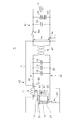
検査装置1は、電源Eや電源ノイズフィルタ用の大容量(例えば4700μF×2)の電解コンデンサC1、C2及び平行平板のコンデンサC3、電流センサSa等を備え、約1200Vの出力電圧Voを出力する電源側回路41と、この電源側回路41にスイッチSwを介して接続された治具側回路43とを備えている。
治具側回路43は、IGBT3に試験電圧を印加するための印加回路45を有し、この印加回路45が、低インダクタンス負荷ケーブル47を介して電源側回路41に接続される。
FIG. 3 is a circuit diagram of the
The
The
印加回路45は、例えば1.2μFのノイズフィルタ用のコンデンサC4〜C5を備え、電源側回路41の高圧側49を、コレクタ用のコンタクトコネクタ17を介してIGBT3のコレクタ電極に接続し、また、低圧側51をエミッタ用のコンタクトコネクタ15を介してIGBT3のエミッタ電極6に接続して閉ループ回路を形成する。高圧側49には、インダクタンスL1が介挿され、また、IGBT3のコレクタとエミッタとの間にはスナバ回路53が設けられている。
またIGBT3のゲート電極4、エミッタ電極6及びエミッタセンス電極8のそれぞれには、検査用回路27に接続されるプローブライン61も別途に接続可能に構成されている。
The
In addition, a
そして、IGBT3の試験時には、検査用治具7がIGBT3に相対的に接近することで、コンタクトコネクタ15、17が、それぞれ電極面12、エミッタ電極6に接触し、コレクタ・エミッタ間に試験電圧を印加する閉ループが形成される。
上述のように、コレクタ・エミッタ間には試験電圧として1000Vの高電圧が印加されるため、各コンタクトコネクタ15、17のそれぞれは、電極との接触時に該電極へ有害な傷付きを生じることがなく、また、大電流を流すことができるような低接触抵抗を実現可能とすべく、そのコンタクトに、コイルばねが用いられている。コイルばねを用いることで、ピンコンタクトに比較して接触点の数を2倍とし、また、接触面積も2倍としている。
このようなコンタクトコネクタ15、17の詳細について、以下では、エミッタ用のコンタクトコネクタ15を代表して説明する。
When testing the
As described above, since a high voltage of 1000 V is applied as a test voltage between the collector and the emitter, each of the
The details of the
図4はコンタクトコネクタ15の構成を示す図であり、図4(A)はコンタクトコネクタ15の平面図、図4(B)はコンタクトコネクタ15を横方向からみた図である。また、図5は、コンタクトコネクタ15をエミッタ電極6に押し付けた状態を示す図であり、図5(A)は該状態を、コイルばねコンタクト21の横方向からみた図、図5(B)は該状態をコイルばねコンタクト21の軸方向からみた図である。
コンタクトコネクタ15は、上述したように、エミッタ電極6に対応して複数のコイルばねコンタクト21を備えるものである。具体的には、エミッタ用コンタクトブロック23の底面23Aには、保持カバー85で覆われた収容凹部24が設けられており、この収容凹部24内にコイルばねコンタクト21が収容されている。
4A and 4B are diagrams showing the configuration of the
As described above, the
それぞれのコイルばねコンタクト21は、収容凹部24内でエミッタ電極6同士の離間距離Xに合せた隙間を設けて互いに並列に配置されている。収容凹部24の底面24Aは、エミッタ電極6と対になる電極面として形成されており、コイルばねコンタクト21がエミッタ電極6に接触することで該エミッタ電極6と導通状態となる。この底面24Aには各コイルばねコンタクト21の取付位置に、該コイルばねコンタクト21の外周の曲率に合せた断面R形状を有するR形状溝75(図5(B))が設けられており、このR形状溝75により位置決めされている。
The
また各コイルばねコンタクト21は、図4(A)に示すように、その長さMがエミッタ電極6を超えない長さに形成されており、また各コイルばねコンタクト21の径Wは、エミッタ電極6の幅と同等に形成されている。
Further, as shown in FIG. 4A, each
上記保持カバー85は、収容凹部24に収容された各コイルばねコンタクト21を覆って保持する絶縁材もしくは絶縁処理された板状であり、エミッタ用コンタクトブロック23にねじ止め固定されている。保持カバー85の固定構造がねじ止めであるため、例えばワーク破壊等の不良発生時にエミッタ電極6の材料であるアルミニウムがコイルばねコンタクト21に付着した場合でも、保持カバー85のねじ止めを取り外して収容凹部24内のコイルばねコンタクト21を簡単に交換できる。
The holding
この保持カバー85には、コイルばねコンタクト21の配置に合せて略矩形の保持開口87が形成されている。各保持開口87は、その全幅Yがコイルばねコンタクト21の径Wよりも狭い幅に形成され、収容凹部24内の落下を防止しつつ、それぞれの保持開口87からコイルばねコンタクト21の外周部の一部を突出させている。
このように各コイルばねコンタクト21は幅狭の保持開口87に係合して保持されるだけなのでコイルばねコンタクト21の交換が簡単になる。
A substantially rectangular holding
As described above, since each
また、コイルばねコンタクト21は、図4(B)に示すように、コイル81のそれぞれを側面視したとききに、コイル81の開始端81Aが前段のコイル81の幅D内に位置するように金属線を巻き回して構成され、図5(A)に示すように、コイルばねコンタクト21の外周部にエミッタ電極6が接触して押し付けられたときには、該コイルばねコンタクト21の軸方向に沿って同じ向きGに倒れるように各コイル81が弾性変形する。
Further, as shown in FIG. 4B, the
すなわち、エミッタ電極6とエミッタ用コンタクトブロック23の間で図5(B)に示すように、コイルばねコンタクト21がコイル81の径方向に押圧された場合でも、各コイルばねコンタクト21の径Wの増大が抑制される。このため、隣合うコイルばねコンタクト21への干渉が防止されることから、コイルばねコンタクト21の隙間を小さくすることが可能となり、高密度に配置された電極に対応することができる。
さらに、各コイルばねコンタクト21は幅狭の保持開口87に係合して保持されるだけであり、該保持カバー85によって弾性変形が制限されることがないため、各コイル81が均一に倒れるように弾性変形しエミッタ電極6に均一に接触させることができる。
That is, even when the
Further, each
また、図5(B)に示すように、保持開口87の両端部87A、87Bに、コイルばねコンタクト21の端部のコイル81が当接することで、方向Gと反対方向への倒れが規制される。これにより、エミッタ電極6がコイルばねコンタクト21の外周部に接触したときに、該コイルばねコンタクト21の端部のコイル81が、方向Gとは逆向きに倒れて立ち上がってしまい、エミッタ電極6へのあたりが強くなるのが防止される。
Further, as shown in FIG. 5B, the
ここで、コイルばねコンタクト21の外周部にエミッタ電極6が接触したときには、図5(A)に示すように、コイルばねコンタクト21のコイル81の倒れに合せて両端部22A、22Bが収容凹部24のR形状溝75に沿って倒れ方向とは反対に移動する。このとき、何ら対策を施さないと、保持開口87から露出していたコイルばねコンタクト21の外周部が保持カバー85の裏側に入り込み、エミッタ電極6を離間させてもコイルばねコンタクト21が保持カバー85に潜り込んだままとなり、試験の中断を招くこととなる。
そこで、収容凹部24の底面24Aには、コイルばねコンタクト21の端部22Aの移動を制限してコイル81の過度な倒れを制限する規制部材としての突起部88が設けられている。この突起部88により、コイルばねコンタクト21の移動とコイル81の過度な倒れが制限されるため、コイルばねコンタクト21が保持カバー85に潜り込むことが防止される。
Here, when the
Therefore, the
ここでエミッタ電極6が高密度化するなどして、コイルばねコンタクト21同士の隙間が狭くなると、エミッタ電極6との接触時に、コイルばねコンタクト21が幅方向に多少弾性変形した際に接触するようになる。このIGBT3では、各エミッタ電極6が同電位に形成され、また、検査装置1が全てのエミッタ電極6に同時に電圧を印加するため、コイルばねコンタクト21同士が接触しても問題は無い。しかしながら、コイルばねコンタクト21同士に接触が発生すると、一方のコイルばねコンタクト21の外周部が他方に入り込み、コイルばねコンタクト21同士で絡まりが発生する虞がある。このような絡まりが発生すると、エミッタ電極6の接触時にコイル81の倒れが制限されることとなるから、コイルばねコンタクト21のエミッタ電極6へのあたりが強くなって該エミッタ電極6が損傷する可能性がある。
そこで、本コンタクトコネクタ15においては、各コイルばねコンタクト21を、図4(A)に示すように、コイル81の軸方向に沿った向きGに倒れるコイルばねコンタクト21Aと、軸方向に沿った逆向きG’にコイル81が倒れるコイルばねコンタクト21B(図5(B)には想像線で示す)とを交互に配置しており、これにより、コイルばねコンタクト21A同士の絡まりを防止してエミッタ電極6へのあたりが強くなるのが防止される。
Here, when the gap between the
Therefore, in this
このように本実施形態によれば、コイルばねコンタクト21の各コイル81が軸方向の同じ向きGに向って倒れるように弾性変形するようにした。このため、コイルばねコンタクト21の幅方向(径方向)への変形が抑制されるため、コイルばねコンタクト21同士が干渉することがなく高密度化が可能となる。
さらに、かかるコイルばねコンタクト21を保持カバー85の径よりも幅狭の保持開口87に係合させて保持されているため、コイルばねコンタクト21の弾性変形が保持カバー85により阻害されることがなく、ワークに対して均一な接触を確保可能することができる。
また保持カバー85の保持開口87にコイルばねコンタクト21を係合させているだけなので当該コイルばねコンタクト21の交換が容易となる。
Thus, according to the present embodiment, the
Further, since the
Further, since the
さらに本実施形態によれば、外周部が押圧されたときに、隣り合うコイルばねコンタクト21間でコイル81の倒れる向きを互いに反対にしたため、隣り合うコイルばねコンタクト21同士が接触したとしても絡まりが発生することがない。これにより、絡まりによりコイル81の倒れが制限されてエミッタ電極6へのあたりが強くなる、ということが防止される。
Furthermore, according to the present embodiment, when the outer peripheral portion is pressed, the directions in which the
また、エミッタ電極6との接触時に、コイルばねコンタクト21の端部22Aの軸方向の移動を規制してコイル81の倒れを制限する規制部材としての突起部88を収容凹部24の底面24Aに設けたため、コイルばねコンタクト21が保持開口87から内部へ潜り込むことが防止可能となる。
Further, a
<第2実施形態>
図6は、本発明の第2実施形態に係るコンタクトコネクタ115の構成を示す図であり、図6(A)はコンタクトコネクタ115の平面図、図6(B)はコンタクトコネクタ115を横方向からみた図である。なお、この図において、図4に示した部材については、同一の符号を付し、その説明を省略する。
Second Embodiment
6A and 6B are diagrams showing the configuration of the
図6(A)に示すように、本実施形態では、保持カバー85の保持開口87の幅Yが、コイルばねコンタクト21の径Wよりも広く形成されており、その両端部87A、87Bには、それぞれコイルばねコンタクト21の径Wよりも狭い幅の幅狭部89が設けられている。この幅狭部89により、図6(B)に示すように、コイルばねコンタクト21が保持カバー85に載った状態においては、該コイルばねコンタクト21の端部22A、22Bが引っ掛かって保持されて落下が防止されている。
As shown in FIG. 6A, in this embodiment, the width Y of the holding
このようなコイルばねコンタクト21の保持構造においては、図6(B)に示すように、保持開口87の端部87A、87Bの両方にコイルばねコンタクト21のコイル81が当接状態となるのではなく、少なくともいずれかの端部側(図示例では、端部22B側)には、保持開口87の端部87A、87B(図示例では端部87B)との間に、エミッタ電極6との接触時に端部22B側のコイル81の移動を許容する隙間Sを形成できる。
これにより、本実施形態によれば、隙間Sの分だけコイルばねコンタクト21の端部22A側の倒れの弾性変形のためのストロークを大きくすることができ、小さなコイルばねコンタクト21でも大きなストローク(倒れ)を実現することができる。
また、コイルばねコンタクト21の一方の端部22B側のコイル81にあっては、保持開口87の端部87Aに当接した状態とされるから、第1実施形態と同様に、エミッタ電極6がコイルばねコンタクト21の外周部に接触したときに、該コイル81が、方向Gとは逆向きに倒れて立ち上がってしまい、エミッタ電極6へのあたりが強くなるのが防止される。
In such a holding structure of the
Thereby, according to this embodiment, the stroke for the elastic deformation of the fall on the end 22 </ b> A side of the
Further, since the
なお、上述した実施形態は、あくまでも本発明の一態様を示すものであり、本発明の範囲内で任意に変形および応用が可能である。 In addition, embodiment mentioned above shows the one aspect | mode of this invention to the last, and a deformation | transformation and application are arbitrarily possible within the scope of the present invention.
例えば、上述した実施形態では、コイルばねコンタクト21の収容凹部24の底面24Aに、位置決めのためのR形状溝75を形成したが、これに限らない。すなわち、各コイルばねコンタクト21を保持カバー85の保持開口87に保持された状態で、該保持カバー85を収容凹部24に取付ける構成とすることで、収容凹部24への位置決めは不要でありR形状溝75を設けなくとも良い。
For example, in the above-described embodiment, the R-shaped
例えば、上述した実施形態では、複数のコイルばねコンタクト21を並列に1列だけ配置した構成を例示したが、これに限らず、並列に配置したコイルばねコンタクト21の組みを軸方向に複数列配置しても良い。
For example, in the above-described embodiment, the configuration in which only one row of the plurality of
1 検査装置
3 IGBT(半導体デバイス)
6 エミッタ電極
9 コンタクトフレーム
15、17、19、115 コンタクトコネクタ
21、21A、21B コイルばねコンタクト
23 エミッタ用コンタクトブロック
23A 底面(電極面)
75 R形状溝
77 隙間
81 コイル
85 保持カバー
87 保持開口
88 突起部(規制部材)
89 幅狭部
X 離間距離
G 倒れの向き
S 隙間
1
6
75 R-shaped groove 77
89 Narrow part X Separation distance G Direction of fall S Gap
Claims (3)
前記コイルばねコンタクトの径よりも幅が狭い幅狭部を少なくとも一部に有する複数の保持開口が形成され、前記保持開口のそれぞれに前記コイルばねコンタクトを該コイルばねコンタクトの外周部を一部突出させて前記幅狭部で保持する保持カバーと、
底面に前記接触電極が形成された凹部に複数の前記コイルばねコンタクトが収められ、前記保持カバーで覆われたブロックと、を備え、
前記保持カバーに保持されたコイルばねコンタクトの各々は、
隣り合うコイルばねコンタクト間で前記コイルの倒れる向きを互いに反対にされ、
前記コイルばねコンタクトの各々が前記ブロックと検査対象の接触電極の間に挟まれたときに、各コイルばねコンタクトにおけるコイルのそれぞれが軸方向の同じ向きに倒れるように弾性変形することを特徴とするコンタクトコネクタ。 A plurality of coil spring contacts formed by winding a metal wire so that the starting end of the coil is positioned within the width of the coil of the previous stage in a side view, which is sandwiched between a pair of contact electrodes and conducts each contact electrode ,
A plurality of holding openings having at least a part of a narrow portion whose width is narrower than the diameter of the coil spring contact is formed, and the coil spring contact protrudes partially from the outer periphery of the coil spring contact in each of the holding openings. A holding cover that holds the narrow portion ;
A plurality of the coil spring contacts are housed in a recess in which the contact electrode is formed on the bottom surface, and the block is covered with the holding cover.
Each of the coil spring contacts held by the holding cover is
The direction in which the coil falls between adjacent coil spring contacts is opposite to each other,
When each of the coil spring contacts is sandwiched between the block and a contact electrode to be inspected , each of the coils in each coil spring contact is elastically deformed so as to fall in the same axial direction. Contact connector.
Priority Applications (1)
| Application Number | Priority Date | Filing Date | Title |
|---|---|---|---|
| JP2009084075A JP5259473B2 (en) | 2009-03-31 | 2009-03-31 | Contact connector |
Applications Claiming Priority (1)
| Application Number | Priority Date | Filing Date | Title |
|---|---|---|---|
| JP2009084075A JP5259473B2 (en) | 2009-03-31 | 2009-03-31 | Contact connector |
Publications (2)
| Publication Number | Publication Date |
|---|---|
| JP2010238466A JP2010238466A (en) | 2010-10-21 |
| JP5259473B2 true JP5259473B2 (en) | 2013-08-07 |
Family
ID=43092628
Family Applications (1)
| Application Number | Title | Priority Date | Filing Date |
|---|---|---|---|
| JP2009084075A Expired - Fee Related JP5259473B2 (en) | 2009-03-31 | 2009-03-31 | Contact connector |
Country Status (1)
| Country | Link |
|---|---|
| JP (1) | JP5259473B2 (en) |
Families Citing this family (4)
| Publication number | Priority date | Publication date | Assignee | Title |
|---|---|---|---|---|
| JP6340666B2 (en) * | 2014-08-25 | 2018-06-13 | 北川工業株式会社 | Conductive member |
| CN108695652B (en) * | 2017-04-11 | 2024-10-29 | 连展科技(深圳)有限公司 | Plug electrical connector |
| JP2019216068A (en) * | 2018-06-14 | 2019-12-19 | 矢崎総業株式会社 | connector |
| JP2025177120A (en) * | 2024-05-22 | 2025-12-05 | Astemo株式会社 | Noise Filter Device |
Family Cites Families (3)
| Publication number | Priority date | Publication date | Assignee | Title |
|---|---|---|---|---|
| JP2000268901A (en) * | 1999-03-18 | 2000-09-29 | Yokowo Co Ltd | Connector of coil spring contact type |
| JP2002075502A (en) * | 2000-08-24 | 2002-03-15 | Fuji Kobunshi Kogyo Kk | Electrical connection method, electrical connector, and electronic component holder |
| JP2002252068A (en) * | 2001-02-26 | 2002-09-06 | Nec Corp | Contact and ic receptacle |
-
2009
- 2009-03-31 JP JP2009084075A patent/JP5259473B2/en not_active Expired - Fee Related
Also Published As
| Publication number | Publication date |
|---|---|
| JP2010238466A (en) | 2010-10-21 |
Similar Documents
| Publication | Publication Date | Title |
|---|---|---|
| KR101582432B1 (en) | Probe unit | |
| KR101552553B1 (en) | A contact probe for the test device | |
| JP5259473B2 (en) | Contact connector | |
| CN105448470A (en) | Header for mounting a planar transformer on a mother board | |
| JP2016048635A (en) | Power storage device | |
| JP2006302906A (en) | Socket for integrated circuit element and circuit board | |
| KR101782600B1 (en) | Apparatus for testing semiconductor package | |
| KR102541773B1 (en) | Contact terminal and ic socket including the same | |
| KR101004708B1 (en) | Probe Device for Semiconductor Package Inspection | |
| JP2016219778A (en) | Power semiconductor device | |
| JP2003172748A (en) | Conductive contact | |
| KR101363367B1 (en) | Examination apparatus of printed circuit board | |
| CN109716604B (en) | Discharge device | |
| US20190123458A1 (en) | Socket | |
| US11515088B2 (en) | Onboard power source device | |
| KR101823119B1 (en) | Relay socket, relay socket module, and test board for semiconductor package | |
| KR101479929B1 (en) | needle block for semiconductor test apparatus improving performance in high frequency | |
| JP2022036615A (en) | Electrical contact structure of electrical contact, and electrical connection device | |
| JP2019178999A (en) | Electric probe and electric connection device | |
| JP5567523B2 (en) | Connection pin | |
| KR20070106935A (en) | Bump structure, its formation method, and semiconductor device using the same | |
| JP6567954B2 (en) | Socket for electrical parts | |
| KR101819355B1 (en) | Probe Fixture by Assembling After Shift Tension | |
| KR102912312B1 (en) | Needle unit for electrical properties inspection device | |
| CN222088591U (en) | Power device packaging structure |
Legal Events
| Date | Code | Title | Description |
|---|---|---|---|
| A621 | Written request for application examination |
Free format text: JAPANESE INTERMEDIATE CODE: A621 Effective date: 20111124 |
|
| A521 | Written amendment |
Free format text: JAPANESE INTERMEDIATE CODE: A523 Effective date: 20120517 |
|
| A977 | Report on retrieval |
Free format text: JAPANESE INTERMEDIATE CODE: A971007 Effective date: 20121217 |
|
| A131 | Notification of reasons for refusal |
Free format text: JAPANESE INTERMEDIATE CODE: A131 Effective date: 20121225 |
|
| A521 | Written amendment |
Free format text: JAPANESE INTERMEDIATE CODE: A523 Effective date: 20130225 |
|
| RD02 | Notification of acceptance of power of attorney |
Free format text: JAPANESE INTERMEDIATE CODE: A7422 Effective date: 20130225 |
|
| TRDD | Decision of grant or rejection written | ||
| A01 | Written decision to grant a patent or to grant a registration (utility model) |
Free format text: JAPANESE INTERMEDIATE CODE: A01 Effective date: 20130416 |
|
| A61 | First payment of annual fees (during grant procedure) |
Free format text: JAPANESE INTERMEDIATE CODE: A61 Effective date: 20130424 |
|
| FPAY | Renewal fee payment (event date is renewal date of database) |
Free format text: PAYMENT UNTIL: 20160502 Year of fee payment: 3 |
|
| R150 | Certificate of patent or registration of utility model |
Free format text: JAPANESE INTERMEDIATE CODE: R150 |
|
| LAPS | Cancellation because of no payment of annual fees |