JP5259242B2 - Three-dimensional stacked nonvolatile semiconductor memory - Google Patents
Three-dimensional stacked nonvolatile semiconductor memory Download PDFInfo
- Publication number
- JP5259242B2 JP5259242B2 JP2008112660A JP2008112660A JP5259242B2 JP 5259242 B2 JP5259242 B2 JP 5259242B2 JP 2008112660 A JP2008112660 A JP 2008112660A JP 2008112660 A JP2008112660 A JP 2008112660A JP 5259242 B2 JP5259242 B2 JP 5259242B2
- Authority
- JP
- Japan
- Prior art keywords
- memory cell
- potential
- bit line
- select gate
- memory
- Prior art date
- Legal status (The legal status is an assumption and is not a legal conclusion. Google has not performed a legal analysis and makes no representation as to the accuracy of the status listed.)
- Active
Links
Images


Classifications
-
- G—PHYSICS
- G11—INFORMATION STORAGE
- G11C—STATIC STORES
- G11C16/00—Erasable programmable read-only memories
- G11C16/02—Erasable programmable read-only memories electrically programmable
- G11C16/04—Erasable programmable read-only memories electrically programmable using variable threshold transistors, e.g. FAMOS
-
- G—PHYSICS
- G11—INFORMATION STORAGE
- G11C—STATIC STORES
- G11C5/00—Details of stores covered by group G11C11/00
- G11C5/02—Disposition of storage elements, e.g. in the form of a matrix array
-
- G—PHYSICS
- G11—INFORMATION STORAGE
- G11C—STATIC STORES
- G11C16/00—Erasable programmable read-only memories
- G11C16/02—Erasable programmable read-only memories electrically programmable
- G11C16/04—Erasable programmable read-only memories electrically programmable using variable threshold transistors, e.g. FAMOS
- G11C16/0483—Erasable programmable read-only memories electrically programmable using variable threshold transistors, e.g. FAMOS comprising cells having several storage transistors connected in series
-
- G—PHYSICS
- G11—INFORMATION STORAGE
- G11C—STATIC STORES
- G11C16/00—Erasable programmable read-only memories
- G11C16/02—Erasable programmable read-only memories electrically programmable
- G11C16/06—Auxiliary circuits, e.g. for writing into memory
- G11C16/08—Address circuits; Decoders; Word-line control circuits
-
- G—PHYSICS
- G11—INFORMATION STORAGE
- G11C—STATIC STORES
- G11C16/00—Erasable programmable read-only memories
- G11C16/02—Erasable programmable read-only memories electrically programmable
- G11C16/06—Auxiliary circuits, e.g. for writing into memory
- G11C16/26—Sensing or reading circuits; Data output circuits
-
- G—PHYSICS
- G11—INFORMATION STORAGE
- G11C—STATIC STORES
- G11C16/00—Erasable programmable read-only memories
- G11C16/02—Erasable programmable read-only memories electrically programmable
- G11C16/06—Auxiliary circuits, e.g. for writing into memory
- G11C16/34—Determination of programming status, e.g. threshold voltage, overprogramming or underprogramming, retention
- G11C16/3418—Disturbance prevention or evaluation; Refreshing of disturbed memory data
- G11C16/3422—Circuits or methods to evaluate read or write disturbance in nonvolatile memory, without steps to mitigate the problem
-
- G—PHYSICS
- G11—INFORMATION STORAGE
- G11C—STATIC STORES
- G11C5/00—Details of stores covered by group G11C11/00
- G11C5/06—Arrangements for interconnecting storage elements electrically, e.g. by wiring
- G11C5/063—Voltage and signal distribution in integrated semi-conductor memory access lines, e.g. word-line, bit-line, cross-over resistance, propagation delay
Landscapes
- Engineering & Computer Science (AREA)
- Microelectronics & Electronic Packaging (AREA)
- Non-Volatile Memory (AREA)
- Semiconductor Memories (AREA)
- Read Only Memory (AREA)
Description
本発明は、三次元積層不揮発性半導体メモリ(3D-stacked nonvolatile semiconductor memory)に関する。 The present invention relates to a three-dimensional stacked nonvolatile semiconductor memory.
三次元構造により大容量化を図りビットコストを抑える技術としてBiCS (Bit Cost Scalable)技術が知られている(例えば、非特許文献1を参照)。 A BiCS (Bit Cost Scalable) technique is known as a technique for increasing the capacity by a three-dimensional structure and suppressing the bit cost (see, for example, Non-Patent Document 1).
BiCS技術が適用された不揮発性半導体メモリ(以下、BiCSメモリ)は、単なる三次元構造ではなく、デバイス構造及びプロセス技術の工夫により、積層数(number of stacked layers)の増加に比例してビットコストが低減するビットコストスケーラビリティを可能にすることを特徴とする。 Non-volatile semiconductor memory to which BiCS technology is applied (hereinafter referred to as BiCS memory) is not just a three-dimensional structure, but the bit cost is proportional to the increase in the number of stacked layers due to device structure and process technology. It enables bit cost scalability to be reduced.
例えば、BiCS技術が適用されたNAND型フラッシュメモリ(以下、BiCS-NANDフラッシュメモリ)の場合には、積層数の増加によりNAND列を構成するセル数を縦方向に増やすことで、二次元構造のNAND型フラッシュメモリのメモリ容量の限界を大幅に上回るメモリ容量を実現する。 For example, in the case of a NAND flash memory to which BiCS technology is applied (hereinafter referred to as “BiCS-NAND flash memory”), the number of cells constituting a NAND row is increased in the vertical direction by increasing the number of stacked layers, thereby providing a two-dimensional structure. Realize memory capacity that greatly exceeds the limit of NAND flash memory capacity.
しかし、BiCS-NANDフラッシュメモリを代表とするBiCSメモリは、独特なデバイス構造を有するため、それを実用化するために解決しなければならない課題も多い。 However, since BiCS memory represented by BiCS-NAND flash memory has a unique device structure, there are many problems to be solved in order to put it into practical use.
その一つに、リードディスターブ(read disturb)がある。 One of them is read disturb.
BiCSメモリは、1本のビット線に接続される1ブロック内のセルユニット数が複数個になる、という特徴を有する。また、回路動作上から、これら複数個のセルユニットを同時に選択することはできない。このため、選択されたブロック内には、リード対象となるメモリセルを含まない非選択のセルユニットが存在することになる。 The BiCS memory has a feature that the number of cell units in one block connected to one bit line is plural. In addition, the plurality of cell units cannot be selected simultaneously in terms of circuit operation. For this reason, there is an unselected cell unit that does not include a memory cell to be read in the selected block.
これは、二次元構造のフラッシュメモリには起こり得なかったことである。 This is not possible in a two-dimensional flash memory.
従って、リード時には、選択されたブロック内の非選択のセルユニット内のメモリセルに閾値電圧の変動が生じないように、リードディスターブについて検討する必要がある。 Therefore, at the time of reading, it is necessary to consider read disturb so that the threshold voltage does not fluctuate in the memory cells in the non-selected cell units in the selected block.
特に、BiCSメモリでは、二次元構造のフラッシュメモリとは異なり、非選択のブロック内のセルユニットにはリード電位及び転送電位を与えなくて済むため、非選択のブロック内のセルユニットに対するリードディスターブについては検討不要である。しかし、選択されたブロック内の非選択のセルユニットがビット線から切断されることに起因して、リード電位が与えられる非選択のメモリセルの閾値状態によっては、そのメモリセルよりもビット線側の非選択のメモリセルに対してリードディスターブによる閾値電圧の変動が生じる。
本発明は、BiCS技術が適用された三次元積層不揮発性半導体メモリのリードディスターブを改善する技術について提案する。 The present invention proposes a technique for improving read disturb of a three-dimensional stacked nonvolatile semiconductor memory to which BiCS technology is applied.
本発明の例に係る三次元積層不揮発性半導体メモリは、半導体基板と、前記半導体基板上において第一方向に並んで配置される第一及び第二ブロックから構成されるメモリセルアレイと、前記メモリセルアレイの前記第一方向に直交する第二方向の一端に配置される第一ドライバとを備える。前記第一及び第二ブロックは、それぞれ、前記半導体基板上に互いに絶縁されてスタックされる3以上の導電層と、前記3以上の導電層上にこれらとは絶縁されて配置されるビット線と、下端が前記半導体基板に接続され、上端が前記ビット線に接続され、前記3以上の導電層を突き抜ける複数の半導体柱とから構成される。前記3以上の導電層のうち最上層は、前記第二方向に延びる複数の第一セレクトゲート線から構成され、前記3以上の導電層のうち最下層は、第二セレクトゲート線であり、前記3以上の導電層のうち前記最上層及び前記最下層を除く残りの導電層は、ワード線である。前記3以上の導電層のうち前記最上層を除く残りの導電層は、前記第一方向の幅が前記複数の第一セレクトゲート線の前記第一方向の幅よりも広いプレート状を有する。前記複数の第一セレクトゲート線の各々と前記複数の半導体柱及び前記第二セレクトゲート線と前記複数の半導体柱とによりそれぞれセレクトゲートトランジスタが構成され、前記ワード線と前記複数の半導体柱とによりそれぞれメモリセルが構成される。前記第一ブロックは、リード対象となるメモリセルを含む選択された第一セルユニット及びリード対象となるメモリセルを含まない非選択の第二セルユニットを有する。前記第二セルユニット内の前記リード電位が印加されるメモリセルよりも前記ビット線側に存在するメモリセルのチャネルに接地電位を与えた状態で前記第一ブロック内の前記ワード線にリード電位又はそれよりも高い転送電位を印加し、この後、前記第二セルユニット内の全てのメモリセルを前記ビット線から切断し、前記ビット線をプリチャージ電位にして、前記第一セルユニット内の前記リード対象となるメモリセルに対してリードを実行する。また、前記リード時に、前記第二ブロック内の前記ワード線には前記リード電位及び前記転送電位が印加されない。 A three-dimensional stacked nonvolatile semiconductor memory according to an example of the present invention includes a semiconductor substrate, a memory cell array including first and second blocks arranged side by side in a first direction on the semiconductor substrate, and the memory cell array. And a first driver disposed at one end in a second direction orthogonal to the first direction. The first and second blocks each include three or more conductive layers that are insulated and stacked on the semiconductor substrate, and a bit line that is disposed on the three or more conductive layers and insulated from them. , And a plurality of semiconductor pillars penetrating through the three or more conductive layers, the lower end being connected to the semiconductor substrate, the upper end being connected to the bit line. The uppermost layer of the three or more conductive layers is composed of a plurality of first select gate lines extending in the second direction, and the lowermost layer of the three or more conductive layers is a second select gate line, Among the three or more conductive layers, the remaining conductive layers excluding the uppermost layer and the lowermost layer are word lines. Of the three or more conductive layers, the remaining conductive layers excluding the uppermost layer have a plate shape in which the width in the first direction is wider than the width in the first direction of the plurality of first select gate lines. Each of the plurality of first select gate lines, the plurality of semiconductor pillars, the second select gate line, and the plurality of semiconductor pillars respectively constitute a select gate transistor, and the word line and the plurality of semiconductor pillars. Each memory cell is configured. The first block includes a selected first cell unit including a memory cell to be read and a non-selected second cell unit not including a memory cell to be read. A read potential or a potential applied to the word line in the first block in a state where a ground potential is applied to the channel of the memory cell existing on the bit line side of the memory cell to which the read potential is applied in the second cell unit A higher transfer potential is applied, and then all the memory cells in the second cell unit are disconnected from the bit line, the bit line is set to a precharge potential, and the memory cell in the first cell unit is Read is performed on the memory cell to be read. Further, the read potential and the transfer potential are not applied to the word line in the second block during the read.
本発明によれば、BiCS技術が適用された三次元積層不揮発性半導体メモリのリードディスターブを改善することができる。 According to the present invention, read disturb of a three-dimensional stacked nonvolatile semiconductor memory to which BiCS technology is applied can be improved.
以下、図面を参照しながら、本発明の例を実施するための最良の形態について詳細に説明する。 The best mode for carrying out an example of the present invention will be described below in detail with reference to the drawings.
1. 概要
本発明の例では、BiCSメモリ特有の構造に起因するリードディスターブ、即ち、選択されたブロック内の非選択のセルユニット内のメモリセルの閾値変動を防止するためのリード手法について提案する。
1. Overview
The example of the present invention proposes a read technique for preventing read disturb caused by a structure unique to a BiCS memory, that is, a threshold fluctuation of a memory cell in an unselected cell unit in a selected block.
BiCSメモリの特徴を回路的に一言でいうと、1本のビット線に接続される1ブロック内のセルユニット数が複数個である、ということになる。この場合、回路動作上、これら複数個のセルユニットを同時に選択することはできない。従って、リード時には、1本のビット線に接続される複数個のセルユニットのうちの1つを選択しなければならない。 In terms of the characteristics of the BiCS memory, the number of cell units in one block connected to one bit line is plural. In this case, the plurality of cell units cannot be selected simultaneously for circuit operation. Therefore, at the time of reading, one of a plurality of cell units connected to one bit line must be selected.
つまり、選択されたブロック内のリード対象となるメモリセルを含まない非選択のセルユニットは、リード時にビット線から切断されることになる。 That is, a non-selected cell unit that does not include a memory cell to be read in the selected block is disconnected from the bit line at the time of reading.
また、非選択のセルユニット内のリード電位が与えられる非選択のメモリセルの閾値状態が、高い閾値状態、例えば、2値記憶(“0”/”1”)の”0”状態である場合には、その非選択のメモリセルは、リード電位が印加される前後においてオフを維持する。 In addition, the threshold state of the non-selected memory cell to which the read potential in the non-selected cell unit is applied is a high threshold state, for example, “0” state of binary storage (“0” / “1”) The unselected memory cell is kept off before and after the read potential is applied.
このため、非選択のセルユニット内のリード電位が与えられるメモリセルよりもビット線側に存在するメモリセルのチャネルは、フローティング状態であり、かつ、リード電位が印加されたときに容量カップリングによりチャネルブーストされる。 For this reason, the channel of the memory cell existing on the bit line side from the memory cell to which the read potential in the non-selected cell unit is applied is in a floating state, and when the read potential is applied, the capacitance coupling causes Channel boosted.
一方、BiCSメモリでは、リード時には、非選択のセルユニット内のリード電位が与えられるメモリセルよりもソース線側に存在するメモリセルのチャネルは、ソース線から接地電位が転送される。 On the other hand, in the BiCS memory, at the time of reading, the ground potential is transferred from the source line to the channel of the memory cell existing on the source line side of the memory cell to which the read potential in the non-selected cell unit is applied.
従って、非選択のセルユニット内のリード電位が与えられるメモリセルには、ソース及びドレイン間に大きな電位差が発生し、それが原因となり、そのメモリセルのソース及びドレイン間にパンチスルーが発生する。 Therefore, a large potential difference is generated between the source and the drain of the memory cell to which the read potential in the non-selected cell unit is applied, which causes the punch-through between the source and the drain of the memory cell.
このパンチスルーに起因してホットキャリアが発生し、このホットキャリアが非選択のセルユニット内のリード電位が与えられるメモリセルよりもビット線側に存在するメモリセルの電荷蓄積層に注入され、閾値電圧の変動が生じる。 Hot carriers are generated due to this punch-through, and the hot carriers are injected into the charge storage layer of the memory cell existing on the bit line side of the memory cell to which the read potential in the non-selected cell unit is applied, and the threshold value Voltage fluctuations occur.
このようなリードディスターブを防止するには、リード時に、非選択のセルユニット内のリード電位が与えられるメモリセルのソース及びドレイン間に大きな電位差が発生しないように、動作タイミングを工夫すればよい。 In order to prevent such read disturb, the operation timing may be devised so that a large potential difference does not occur between the source and drain of the memory cell to which the read potential in the non-selected cell unit is applied at the time of reading.
そこで、本発明の例では、リード時に、選択されたブロック内の非選択のセルユニット内のリード電位が印加されるメモリセルよりもビット線側に存在するメモリセルのチャネルに接地電位を与え、これによりチャネルブーストを防止するリード手法を提案する。 Therefore, in the example of the present invention, at the time of reading, a ground potential is applied to the channel of the memory cell existing on the bit line side from the memory cell to which the read potential in the non-selected cell unit in the selected block is applied, This proposes a lead technique that prevents channel boost.
具体的には、選択されたブロック内の非選択のセルユニット内のリード電位が印加されるメモリセルよりもビット線側に存在するメモリセルのチャネルに接地電位を与えた状態で選択されたブロック内のワード線にリード電位又はそれよりも高い転送電位を印加し、この後、非選択のセルユニット内の全てのメモリセルをビット線から切断し、ビット線をプリチャージ電位にして、選択されたセルユニット内のリード対象となるメモリセルに対してリードを実行する。 Specifically, the selected block in a state where the ground potential is applied to the channel of the memory cell existing on the bit line side of the memory cell to which the read potential in the non-selected cell unit in the selected block is applied. A read potential or a higher transfer potential is applied to the word line in the memory cell, and then all memory cells in the unselected cell unit are disconnected from the bit line, and the bit line is set to the precharge potential. The memory cell to be read in the cell unit is read.
接地電位は、例えば、ビット線から、非選択のセルユニット内のリード電位が印加されるメモリセルよりもビット線側に存在するメモリセルのチャネルに転送する。 For example, the ground potential is transferred from the bit line to the channel of the memory cell existing on the bit line side of the memory cell to which the read potential in the non-selected cell unit is applied.
これにより、選択されたブロック内のワード線にリード電位又はそれよりも高い転送電位を印加したときに、非選択のセルユニット内のリード電位が印加されるメモリセルよりもビット線側に存在するメモリセルのチャネルがブーストされることはなく、リードディスターブを改善することができる。 Thus, when a read potential or a transfer potential higher than the read potential is applied to the word line in the selected block, the read potential in the non-selected cell unit exists on the bit line side from the memory cell to which the read potential is applied. The channel of the memory cell is not boosted, and read disturb can be improved.
2. BiCSメモリ
(1) 基本構造
まず、BiCSメモリの基本構造について説明する。
2. BiCS memory
(1) Basic structure
First, the basic structure of the BiCS memory will be described.
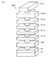
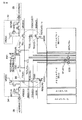
図1は、BiCS-NANDフラッシュメモリの鳥瞰図を示している。 FIG. 1 shows a bird's-eye view of a BiCS-NAND flash memory.
NANDフラッシュメモリは、例えば、各々が消去の一単位となる複数のブロックから構成される。ここでは、二つのブロックBK<i>, BK<i+1>について図示する。 The NAND flash memory is composed of, for example, a plurality of blocks each serving as a unit of erasure. Here, two blocks BK <i> and BK <i + 1> are illustrated.
半導体基板内に形成されるソース拡散層24は、例えば、全てのブロックに共通に1つ設けられる。ソース拡散層24は、コンタクトプラグPSLを介して、ソース線SL・M1に接続される。また、ソース拡散層24上には、例えば、導電性ポリシリコンから構成される3以上の導電層が積層される(本例では6層構造)。
For example, one
最上層を除く残りの5つの導電層は、1つのブロックBK<i+1>内でそれぞれプレート状に形成され、かつ、そのX方向の端部は、各々の導電層にコンタクトをとるために階段状に形成される。最下層は、ソース線側セレクトゲート線SGSとなり、最下層及び最上層を除く残りの4つの導電層は、ワード線WL<0>, WL<1>, WL<2>, WL<3>となる。 The remaining five conductive layers excluding the top layer are each formed in a plate shape within one block BK <i + 1>, and the end in the X direction is used to contact each conductive layer. It is formed in steps. The lowermost layer is the source line side select gate line SGS, and the remaining four conductive layers excluding the lowermost layer and the uppermost layer are word lines WL <0>, WL <1>, WL <2>, WL <3>. Become.
最上層は、X方向に延びるライン状の複数の導電線から構成される。1つのブロックBK<i+1>内には、例えば、6本の導電線が配置される。最上層の例えば6本の導電線は、ビット線側セレクトゲート線SGD<0>, …SGD<5>となる。 The uppermost layer is composed of a plurality of linear conductive lines extending in the X direction. For example, six conductive lines are arranged in one block BK <i + 1>. For example, six conductive lines in the uppermost layer become bit line side select gate lines SGD <0>,... SGD <5>.
そして、NANDセルユニットを構成するための複数の活性層(アクティブエリア)AAは、複数の導電層を突き抜けてソース拡散層24に達するように、Z方向(半導体基板の表面に対して垂直方向)に柱状に形成される。 Then, the plurality of active layers (active areas) AA for constituting the NAND cell unit penetrates the plurality of conductive layers and reaches the source diffusion layer 24 (in the direction perpendicular to the surface of the semiconductor substrate). It is formed in a columnar shape.
複数の活性層AAの上端は、Y方向に延びる複数のビット線BL<0>, …BL<m>に接続される。また、ソース線側セレクトゲート線SGSは、コンタクトプラグPSGSを介して、X方向に延びる引き出し線SGS・M1に接続され、ワード線WL<0>, WL<1>, WL<2>, WL<3>は、それぞれ、コンタクトプラグをPWL<0>, PWL<1>, PWL<2>, PWL<3> 介して、X方向に延びる引き出し線WL<0>・M1, WL<1>・M1, WL<2>・M1, WL<3>・M1に接続される。 Upper ends of the plurality of active layers AA are connected to a plurality of bit lines BL <0>,... BL <m> extending in the Y direction. Further, the source line side select gate line SGS is connected to the lead line SGS • M1 extending in the X direction via the contact plug P SGS , and the word lines WL <0>, WL <1>, WL <2>, WL <3> is a lead wire WL <0>, M1, WL extending in the X direction through the contact plugs PWL <0> , PWL <1> , PWL <2> , PWL <3> , respectively. Connected to <1> ・ M1, WL <2> ・ M1, WL <3> ・ M1.
さらに、ビット線側セレクトゲート線SGD<0>, …SGD<5>は、それぞれ、コンタクトプラグPSGD<0>, …PSGD<5>を介して、X方向に延びる引き出し線SGD<0>・M1, …SGD<5>・M1に接続される。 Further, the bit line side select gate line SGD <0>, ... SGD <5> are each, contact plugs P SGD <0>, ... P SGD through <5>, lead line SGD extending in the X direction <0> • M1,… SGD <5> • Connected to M1.
複数のビット線BL<0>, …BL<m>及び引き出し線SGS・M1, WL<0>・M1, WL<1>・M1, WL<2>・M1, WL<3>・M1, SGD<0>・M1, …SGD<5>・M1は、例えば、金属から構成される。 Multiple bit lines BL <0>,… BL <m> and leader lines SGS ・ M1, WL <0> ・ M1, WL <1> ・ M1, WL <2> ・ M1, WL <3> ・ M1, SGD <0> · M1,... SGD <5> · M1 is made of metal, for example.
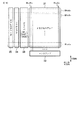
図2は、図1のBiCS-NANDフラッシュメモリの平面図を示している。 FIG. 2 is a plan view of the BiCS-NAND flash memory of FIG.
柱状の複数の活性層AAは、半導体基板の上面から見た場合にアレイ状に配置され、メモリセルアレイ15を構成する。NANDセルユニットは、複数の活性層AAの各々に形成されるが、その詳細については後述する。
The plurality of columnar active layers AA are arranged in an array when viewed from the upper surface of the semiconductor substrate, and constitute the
WLドライバ11-i, 11-(i+1)は、引き出し線WL<0>・M1, WL<1>・M1, WL<2>・M1, WL<3>・M1を介してワード線WL<0>, WL<1>, WL<2>, WL<3>に接続され、これらを書き込み/読み出し/消去時に駆動する。 WL drivers 11-i, 11- (i + 1) are connected to the word line WL via the leader lines WL <0>, M1, WL <1>, M1, WL <2>, M1, WL <3>, and M1. It is connected to <0>, WL <1>, WL <2>, WL <3> and drives them at the time of writing / reading / erasing.
SGSドライバ12-i, 12-(i+1)は、引き出し線SGS・M1を介してソース線側セレクトゲート線SGSに接続される。SGDドライバ13は、引き出し線SGD<0>・M1, …SGD<5>・M1を介してビット線側セレクトゲート線SGD<0>, …SGD<5>に接続される。
The SGS drivers 12-i and 12- (i + 1) are connected to the source line side select gate line SGS via the lead lines SGS · M1. The
SLドライバ14は、ソース線SL・M1を介してソース拡散層24に接続される。
The
このレイアウトでは、周辺回路としてのドライバを構成するトランジスタ数の増加を考慮して、WLドライバ11-i, 11-(i+1)及びSGSドライバ12-i, 12-(i+1)は、メモリセルアレイ15のX方向の一端側に配置され、SGDドライバ13は、メモリセルアレイ15のX方向の他端側に配置される。
In this layout, in consideration of the increase in the number of transistors constituting the driver as a peripheral circuit, the WL drivers 11-i, 11- (i + 1) and the SGS drivers 12-i, 12- (i + 1) The
図3は、図2のIII-III線に沿う断面図である。 3 is a cross-sectional view taken along line III-III in FIG.
P型半導体基板(P-sub)21内には、N型ウェル領域(N-well)22及びP型ウェル領域(P-well)23が形成される。ソース拡散層24は、N型拡散層であり、P型ウェル領域23内に形成される。
In the P-type semiconductor substrate (P-sub) 21, an N-type well region (N-well) 22 and a P-type well region (P-well) 23 are formed. The
P型半導体基板21内には、Nチャネル型FET(例えば、Nチャネル型MOSFET)25が形成され、N型ウェル領域22内には、Pチャネル型FET(例えば、Pチャネル型MOSFET)26が形成される。これらトランジスタは、メモリセルアレイの周辺部に形成される周辺回路(例えば、ドライバ)を構成する。
An N-channel FET (for example, an N-channel MOSFET) 25 is formed in the P-
ソース線側セレクトゲート線SGS及びワード線WL<0>, WL<1>, WL<2>, WL<3>は、第一メタル層M1内の引き出し線及び第一メタル層M1上の第二メタル層M2内の引き出し線を介して、ドライバを構成するトランジスタに接続される。 The source line side select gate line SGS and the word lines WL <0>, WL <1>, WL <2>, WL <3> are the lead lines in the first metal layer M1 and the second lines on the first metal layer M1. It is connected to a transistor constituting a driver through a lead line in the metal layer M2.
ワード線WL<3>を例にとると、ワード線WL<3>は、第一メタル層M1内の引き出し線WL<3>・M1及び第一メタル層M1上の第二メタル層M2内の引き出し線WL<3>・M2を介して、ワード線ドライバを構成するNチャネル型FET 25に接続される。
Taking the word line WL <3> as an example, the word line WL <3> is connected to the lead line WL <3> · M1 in the first metal layer M1 and the second metal layer M2 on the first metal layer M1. It is connected to the N-
ここで、Nチャネル型FET 25及びPチャネル型FET 26のゲート電極は、例えば、ソース線側セレクトゲート線SGSと同時に形成される。
Here, the gate electrodes of the N
即ち、Nチャネル型FET 25及びPチャネル型FET 26のゲート電極は、ソース線側セレクトゲート線SGSと同じ構造及び同じ厚さを有する。
That is, the gate electrodes of the N
図4は、図2のIV-IV線に沿う断面図である。 4 is a cross-sectional view taken along the line IV-IV in FIG.
複数の活性層(アクティブエリア)AAは、ソース線側セレクトゲート線SGS、ワード線WL<0>, WL<1>, WL<2>, WL<3>及びビット線側セレクトゲート線SGD<0>, …SGD<5>を突き抜けて、その一端(最下部)がソース拡散層24に接続され、その他端(最上部)がビット線BL<0>に接続される。
A plurality of active layers (active areas) AA include source line side select gate line SGS, word lines WL <0>, WL <1>, WL <2>, WL <3> and bit line side select gate line SGD <0. >,... Penetrates through SGD <5>, one end (bottom) thereof is connected to the
複数の活性層AAは、Z方向(半導体基板の表面に対して垂直方向)に柱状に形成され、NANDセルユニット NANDは、複数の活性層AAの各々に形成される。 The plurality of active layers AA are formed in a column shape in the Z direction (direction perpendicular to the surface of the semiconductor substrate), and the NAND cell unit NAND is formed in each of the plurality of active layers AA.
NANDセルユニット NANDの構造例を図5に示す。 An example of the NAND cell unit NAND structure is shown in FIG.
メモリセルMCは、MONOS構造を有する。 Memory cell MC has a MONOS structure.
MONOS構造とは、電荷蓄積層が窒化物(nitride)などの絶縁体から構成されるメモリセル構造のことである。ここでは、電荷蓄積層は、多層構造(Charge trap layers)とし、ONO(oxide/nitride/oxide)の例を挙げる。 The MONOS structure is a memory cell structure in which the charge storage layer is made of an insulator such as nitride. Here, the charge storage layer has a multilayer structure (Charge trap layers) and an example of ONO (oxide / nitride / oxide) is given.
セレクトゲートトランジスタSTは、例えば、メモリセルMCと同一構造を有する。 The select gate transistor ST has, for example, the same structure as the memory cell MC.
但し、セレクトゲートトランジスタSTのゲート絶縁膜については、メモリセルMCと異なる構造、即ち、電荷蓄積層を有しない構造(例えば、シリコン酸化膜の単一膜)としてもよい。 However, the gate insulating film of the select gate transistor ST may have a structure different from that of the memory cell MC, that is, a structure having no charge storage layer (for example, a single film of a silicon oxide film).
NANDセルユニットの鳥瞰図を図6に示す。 A bird's-eye view of the NAND cell unit is shown in FIG.
三次元構造のNANDセルユニットの特徴の一つは、ソース線側セレクトゲート線SGS、ワード線WL<0>, WL<1>, WL<2>, WL<3>及びビット線側セレクトゲート線SGD<0>, …SGD<5>が、柱状の活性層AAの側面を取り囲む構造を有している点にある。 One of the features of the three-dimensional NAND cell unit is that the source line side select gate line SGS, word lines WL <0>, WL <1>, WL <2>, WL <3> and bit line side select gate lines SGD <0>,... SGD <5> has a structure surrounding the side surface of the columnar active layer AA.
このため、例えば、複数の活性層AAを細くして、半導体基板上により多くの活性層AAを形成し、大容量化を図っても、NANDセルユニットを構成するトランジスタの駆動力を十分に確保できることにある。 For this reason, for example, a plurality of active layers AA are thinned to form more active layers AA on the semiconductor substrate, and even if the capacity is increased, sufficient drive power for the transistors constituting the NAND cell unit is ensured. There is something you can do.
図7は、メモリセルアレイの等価回路を示している。 FIG. 7 shows an equivalent circuit of the memory cell array.
BiCS-NANDフラッシュメモリは、三次元構造を有するため、これに合わせて、等価回路も三次元的に記載している。 Since the BiCS-NAND flash memory has a three-dimensional structure, an equivalent circuit is also described three-dimensionally.
NAND列を構成するメモリセルの数は、多ければ多いほど大容量化に貢献できるが、BiCS構造の特質から、NAND列を構成するメモリセルの数が多くなるに従い、製造プロセス上、メモリセルの特性にばらつきが生じる可能性がある。 The larger the number of memory cells that make up the NAND string, the greater the capacity that can contribute to the increase in capacity. However, due to the characteristics of the BiCS structure, as the number of memory cells that make up the NAND string increases, There may be variations in characteristics.
このような特性のばらつきを考慮する場合、NAND列を構成するメモリセルの数を少なめ(例えば、4個、8個など)とする。また、図7の等価回路で示される構造の上に、さらに同じ構造を積み重ねてもよい。 In consideration of such characteristic variation, the number of memory cells constituting the NAND string is reduced (for example, four, eight, etc.). Further, the same structure may be further stacked on the structure shown in the equivalent circuit of FIG.
図8は、BiCS-NANDと二次元NANDとを比較して示す図である。 FIG. 8 is a diagram showing a comparison between BiCS-NAND and two-dimensional NAND.
二次元構造のNAND型フラッシュメモリ(二次元NAND)では、1本のビット線BLに接続される1ブロック内のNANDセルユニットの数が1個であるのに対し、BiCS-NANDでは、1本のビット線BLに接続される1ブロック内のNANDセルユニットの数が複数個である。 In the two-dimensional NAND flash memory (two-dimensional NAND), the number of NAND cell units in one block connected to one bit line BL is one, whereas in BiCS-NAND, one There are a plurality of NAND cell units in one block connected to the bit line BL.
従って、以下で説明するように、書き込み動作及び読み出し動作においては、1本のビット線BLに接続される1ブロック内の複数個のセルユニットのうちの1つをビット線側セレクトゲート線SGD<0>, …SGD<5>により選択する。 Therefore, as described below, in the write operation and the read operation, one of the plurality of cell units in one block connected to one bit line BL is connected to the bit line side select gate line SGD < 0>,… Select by SGD <5>.
(2) 基本動作
図1乃至図8のBiCS-NANDフラッシュメモリの基本動作について説明する。
(2) Basic operation
The basic operation of the BiCS-NAND flash memory of FIGS. 1 to 8 will be described.
書き込み/読み出し/消去の基本動作は、二次元構造のNAND型フラッシュメモリと同じであるため、ここでは、BiCS-NANDフラッシュメモリに特有な事項について説明する。 Since the basic operation of writing / reading / erasing is the same as that of a NAND flash memory having a two-dimensional structure, only items specific to the BiCS-NAND flash memory will be described here.
BiCS-NANDフラッシュメモリは、1ブロックの概念が二次元構造のNAND型フラッシュメモリと異なる。 The BiCS-NAND flash memory is different from the NAND flash memory having a two-dimensional structure in the concept of one block.
二次元構造のNAND型フラッシュメモリでは、1本のビット線に接続される1ブロック内のNANDセルユニットの数は1個であるが、BiCS-NANDフラッシュメモリでは、1本のビット線に接続される1ブロック内のNANDセルユニットの数は複数個である。 In a NAND flash memory with a two-dimensional structure, the number of NAND cell units in one block connected to one bit line is one, but in a BiCS-NAND flash memory, it is connected to one bit line. There are a plurality of NAND cell units in one block.
例えば、図2の平面図において、ビット線BL<0>に接続されるブロックBK<i+1>内のNANDセルユニットの数(図中、活性層AAの数に相当)は、6個である。 For example, in the plan view of FIG. 2, the number of NAND cell units (corresponding to the number of active layers AA in the figure) in the block BK <i + 1> connected to the bit line BL <0> is six. is there.
従って、書き込み動作及び読み出し動作においては、ビット線BL<0>に接続されるブロックBK<i+1>内の6個のNANDセルユニットのうちの1つを選択する必要がある。 Therefore, in the write operation and the read operation, it is necessary to select one of the six NAND cell units in the block BK <i + 1> connected to the bit line BL <0>.
この選択は、ビット線側セレクトゲート線SGD<0>, …SGD<5>により行う。ビット線側セレクトゲート線SGD<0>, …SGD<5>は、ブロックBK<i+1>内のY方向の6個のNANDセルユニットに個別に接続される。 This selection is performed by the bit line side select gate lines SGD <0>,... SGD <5>. The bit line side select gate lines SGD <0>,... SGD <5> are individually connected to six NAND cell units in the Y direction in the block BK <i + 1>.
消去動作は、二次元構造のNAND型フラッシュメモリと同様に、例えば、1ブロック内の全てのメモリセルに対して一括して行われる。 The erasing operation is performed on all the memory cells in one block at the same time, for example, as in the NAND flash memory having a two-dimensional structure.
BiCS-NANDフラッシュメモリは、1つのメモリセルに2値データを記憶する2値メモリ、及び、1つのメモリセルに3値以上の多値データを記憶する多値メモリの両方に適用可能である。 The BiCS-NAND flash memory can be applied to both a binary memory that stores binary data in one memory cell and a multi-value memory that stores multi-value data of three or more values in one memory cell.
3. 実施形態
本発明の実施形態について説明する。
3. Embodiment
An embodiment of the present invention will be described.
(1) ブロックレイアウト
図9は、BiCSメモリのブロックレイアウトの第一例を示している。
(1) Block layout
FIG. 9 shows a first example of a block layout of the BiCS memory.
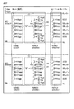
このブロックレイアウトは、例えば、図1のBiCS-NANDフラッシュメモリに対応し、ビット線側セレクトゲート線ドライバをメモリセルアレイの一端に配置し、ワード線ドライバ及びソース線側セレクトゲート線ドライバをメモリセルアレイの他端に配置した点に特徴を有する。 This block layout corresponds to, for example, the BiCS-NAND flash memory of FIG. 1, the bit line side select gate line driver is arranged at one end of the memory cell array, and the word line driver and source line side select gate line driver are arranged in the memory cell array. It is characterized in that it is arranged at the other end.
メモリセルアレイ31のX方向の一端(左側)には、ドライバ33L、レベルシフタ34L及びアドレスデコーダ35Lが配置される。ドライバ33Lは、ビット線側セレクトゲート線SGDを駆動するドライバであり、転送トランジスタを含む。
A
メモリセルアレイ31のX方向の他端(右側)には、ドライバ33R、レベルシフタ34R及びアドレスデコーダ35Rが配置される。ドライバ33Rは、ワード線WL及びソース線側セレクトゲート線SGSを駆動するドライバであり、転送トランジスタを含む。
On the other end (right side) of the
また、メモリセルアレイ31のY方向の一端には、センスアンプ32が配置される。メモリセルアレイ31上には、Y方向に延びるビット線BL<0>, …BL<m>が配置され、ビット線BL<0>, …BL<m>は、センスアンプ32に接続される。
A
このブロックレイアウトは、図1のBiCS-NANDフラッシュメモリに対応するため、ブロックBK<0>, BL<1>, …BK<n>内にそれぞれ複数本のビット線側セレクトゲート線SGDが配置される。即ち、ビット線側セレクトゲート線SGDを駆動するドライバの面積が大きくなるため、メモリセルアレイ32の他端に配置されるワード線ドライバ及びソース線側セレクトゲート線ドライバとは別に、メモリセルアレイ32の一端にビット線側セレクトゲート線ドライバを配置する。
Since this block layout corresponds to the BiCS-NAND flash memory of FIG. 1, a plurality of bit line side select gate lines SGD are arranged in each of the blocks BK <0>, BL <1>,... BK <n>. The That is, since the area of the driver for driving the bit line side select gate line SGD is increased, one end of the
図10は、BiCSメモリのブロックレイアウトの第二例を示している。 FIG. 10 shows a second example of the block layout of the BiCS memory.
第二例の特徴は、第一例と比べると、ワード線WL、ソース線側セレクトゲート線SGS及びビット線側セレクトゲート線SGDを駆動するドライバ33を、まとめて、メモリセルアレイ31の一端に配置した点にある。
Compared to the first example, the feature of the second example is that a
メモリセルアレイ31のX方向の一端(左側)には、ドライバ33、レベルシフタ34及びアドレスデコーダ35が配置される。ドライバ33は、ワード線WL、ソース線側セレクトゲート線SGS及びビット線側セレクトゲート線SGDを駆動するドライバであり、転送トランジスタを含む。
A
また、メモリセルアレイ31のY方向の一端には、センスアンプ32が配置される。メモリセルアレイ31上には、Y方向に延びるビット線BL<0>, …BL<m>が配置され、ビット線BL<0>, …BL<m>は、センスアンプ32に接続される。
A
このように、ワード線WL、ソース線側セレクトゲート線SGS及びビット線側セレクトゲート線SGDを駆動するドライバ33をまとめることで、アドレスデコーダ34及びレベルシフタ35も一つにまとめることができ、周辺回路を効率的にレイアウトすることが可能になる。
In this way, by combining the
しかし、このブロックレイアウトでは、メモリセルアレイ31が巨大化され、さらに、メモリセルの微細化により、ワード線WL、ソース線側セレクトゲート線SGS及びビット線側セレクトゲート線SGDが狭ピッチ化されると、寄生容量による信号遅延が問題となる。
However, in this block layout, when the
特に、BiCSメモリでは、ワード線WL及びソース線側セレクトゲート線SGSがプレート状に形成される。このため、これら導電線間の寄生容量が大きく、カップリングノイズの原因となる。 In particular, in the BiCS memory, the word line WL and the source line side select gate line SGS are formed in a plate shape. For this reason, the parasitic capacitance between these conductive lines is large, which causes coupling noise.
図11は、BiCSメモリのブロックレイアウトの第三例を示している。 FIG. 11 shows a third example of the block layout of the BiCS memory.
第三例の特徴は、第二例と比べると、二つのメモリセルアレイ31L, 31Rを設けた点に特徴を有する。二つのメモリセルアレイ31L, 31Rを設けることで、各メモリセルアレイ内のワード線WL、ソース線側セレクトゲート線SGS及びビット線側セレクトゲート線SGDを短くできるため、信号遅延及びカップリングノイズを抑制できる。
The feature of the third example is different from the second example in that two
メモリセルアレイ31L, 31Rは、X方向に並んで配置される。メモリセルアレイ31L, 31Rの間には、ドライバ33L, 33R、レベルシフタ34及びアドレスデコーダ35が配置される。ドライバ33L, 33Rは、ワード線WL、ソース線側セレクトゲート線SGS及びビット線側セレクトゲート線SGDを駆動するドライバであり、転送トランジスタを含む。
The
また、メモリセルアレイ31L, 31RのY方向の一端には、センスアンプ32L, 32Rが配置される。メモリセルアレイ31L, 31R上には、Y方向に延びるビット線BL<0>, …BL<m>が配置され、ビット線BL<0>, …BL<m>は、センスアンプ32L, 32Rに接続される。
In addition,
このブロックレイアウトでは、レベルシフタ34及びアドレスデコーダ35は、二つのメモリセルアレイ31L, 31Rで共有化されるが、ドライバ33Lは、メモリセルアレイ31Lに対応して設けられ、ドライバ33Rは、メモリセルアレイ31Rに対応して設けられる。
In this block layout, the
このように、二つのメモリセルアレイ31L, 31Rでドライバ33L, 33Rを共有化できない理由は、これらドライバを構成するトランジスタの数が多いため、共有化すると、メモリセルアレイ31L, 31Rとドライバ33L, 33Rとを接続する配線レイアウトが複雑になるからである。即ち、メモリセルアレイごとにドライバを設ければ、二つのメモリセルアレイでドライバを共有する場合よりも配線レイアウトが簡略化される。
As described above, the reason why the
図12は、BiCSメモリのブロックレイアウトの第四例を示している。 FIG. 12 shows a fourth example of the block layout of the BiCS memory.
第四例の特徴は、第三例と比べると、ワード線WL、ソース線側セレクトゲート線SGS及びビット線側セレクトゲート線SGDを駆動するドライバ33を二つのメモリセルアレイ31L, 31Rで共有化した点に特徴を有する。
Compared with the third example, the feature of the fourth example is that the
このドライバ33の共有化は、ドライバ33の面積、即ち、ドライバ33を構成するトランジスタ数を削減することにより実現される。トランジスタ数が削減されれば、メモリセルアレイ31L, 31Rとドライバ33L, 33Rとを接続する配線レイアウトが複雑化しないからである。ドライバ33を構成するトランジスタ数の削減は、本発明に係わるビット線側セレクトゲート線のレイアウトにより達成されるが、それについては後述し、ここでは、ブロックレイアウトについてのみ説明する。
The sharing of the
メモリセルアレイ31L, 31Rは、X方向に並んで配置される。メモリセルアレイ31L, 31Rの間には、ドライバ33、レベルシフタ34及びアドレスデコーダ35が配置される。ドライバ33は、ワード線WL、ソース線側セレクトゲート線SGS及びビット線側セレクトゲート線SGDを駆動するドライバであり、転送トランジスタを含む。
The
また、メモリセルアレイ31L, 31RのY方向の一端には、センスアンプ32L, 32Rが配置される。メモリセルアレイ31L, 31R上には、Y方向に延びるビット線BL<0>, …BL<m>が配置され、ビット線BL<0>, …BL<m>は、センスアンプ32L, 32Rに接続される。
In addition,
このブロックレイアウトでは、ドライバ33、レベルシフタ34及びアドレスデコーダ35は、二つのメモリセルアレイ31L, 31Rで共有化される。
In this block layout, the
尚、配線レイアウトの複雑化なく、ドライバ33を二つのメモリセルアレイ31L, 31Rで共有化できれば、第一例乃至第四例のなかで、この第四例のブロックレイアウトが最も好ましいブロックレイアウトとなる。
If the
(2) ビット線側セレクトゲート線のレイアウト
図13は、ビット線側セレクトゲート線のレイアウトの第一例を示している。図14は、図13をデバイス化にした場合の平面レイアウトを示している。
(2) Layout of select gate line on the bit line side
FIG. 13 shows a first example of the layout of the bit line side select gate lines. FIG. 14 shows a planar layout when FIG. 13 is made into a device.
第一例は、図9のブロックレイアウトに対応する。即ち、ビット線側セレクトゲート線SGD<0>, …SGD<5>に接続されるドライバ33Lは、メモリセルアレイ31のX方向の一端(左側)に配置され、かつ、ワード線WL<0>, …WL<3>及びソース線側セレクトゲート線SGSに接続されるドライバ33Rとは独立に設けられる。
The first example corresponds to the block layout of FIG. That is, the
二つのブロックBK<i>, BK<i+1>は、それぞれ、半導体基板上に互いに絶縁されてスタックされる3以上の導電層と、3以上の導電層上にこれらとは絶縁されて配置されるビット線BL<0>, …BL<m>と、下端が半導体基板に接続され、上端がビット線BL<0>, …BL<m>に接続され、3以上の導電層を突き抜ける複数の活性層(半導体柱)AAとから構成される。 The two blocks BK <i> and BK <i + 1> are respectively arranged on three or more conductive layers that are insulated and stacked on the semiconductor substrate and are insulated from each other on the three or more conductive layers. Bit lines BL <0>,... BL <m> connected to the semiconductor substrate, and the upper ends connected to the bit lines BL <0>,... BL <m> and penetrate through three or more conductive layers. Active layer (semiconductor pillar) AA.
3以上の導電層のうち最上層は、複数のビット線側セレクトゲート線SGD<0>, …SGD<5>から構成され、3以上の導電層のうち最下層は、ソース線側セレクトゲート線SGSであり、3以上の導電層のうち最上層及び最下層を除く残りの導電層は、ワード線WL<0>, …WL<3>である。 Among the three or more conductive layers, the uppermost layer is composed of a plurality of bit line side select gate lines SGD <0>,... SGD <5>, and the lowermost layer of the three or more conductive layers is the source line side select gate line. Of the three or more conductive layers, the remaining conductive layers excluding the uppermost layer and the lowermost layer are word lines WL <0>,... WL <3>.
本例では、1つのブロック内のビット線側セレクトゲート線SGD<0>, …SGD<5>の数が6本、ワード線WL<0>, …WL<3>の数が4本であるが、これに限られることはない。即ち、1つのブロック内のビット線側セレクトゲート線の数については、1本以上、ワード線の数についても、1本以上であればよい。 In this example, the number of bit line side select gate lines SGD <0>,... SGD <5> in one block is 6, and the number of word lines WL <0>,... WL <3> is 4. However, it is not limited to this. That is, the number of bit line side select gate lines in one block may be one or more, and the number of word lines may be one or more.
また、3以上の導電層のうち最上層を除く残りの導電層は、Y方向の幅がビット線側セレクトゲート線SGD<0>, …SGD<5>のY方向の幅よりも広いプレート状を有する。 Of the three or more conductive layers, the remaining conductive layers other than the uppermost layer have a plate shape in which the width in the Y direction is wider than the width in the Y direction of the bit line side select gate lines SGD <0>,. Have
そして、ビット線側セレクトゲート線SGD<0>, …SGD<5>と活性層AAとによりビット線側セレクトゲートトランジスタが構成され、ソース線側セレクトゲート線SGSと活性層AAとによりソース線側セレクトゲートトランジスタが構成される。また、ワード線WL<0>, …WL<3>と活性層AAとによりメモリセルが構成される。 The bit line side select gate line SGD <0>,... SGD <5> and the active layer AA constitute a bit line side select gate transistor, and the source line side select gate line SGS and the active layer AA constitute the source line side. A select gate transistor is configured. Further, a memory cell is constituted by the word lines WL <0>,... WL <3> and the active layer AA.
また、メモリセルアレイ31とドライバ33Lとの間の領域は、両者を接続するための引き出し線(導電線)SGD<0>・M1, …SGD<5>・M1が配置される引き出し部36Lとなる。同様に、メモリセルアレイ31とドライバ33Rとの間の領域は、両者を接続するための引き出し線(導電線)WL<0>・M1, …WL<3>・M1, SGS・M1が配置される引き出し部36Rとなる。
In addition, a region between the
ここで、ブロックBK<i>内のビット線側セレクトゲート線SGD<0>, …SGD<5>とブロックBK<i+1>内のビット線側セレクトゲート線SGD<0>, …SGD<5>とは、メモリセルアレイ31のX方向の一端において一対一に共通接続されたうえでドライバ33Lに接続される。
Here, bit line side select gate lines SGD <0>,… SGD <5> in block BK <i> and bit line side select gate lines SGD <0>,… SGD <in block BK <i + 1> 5> is commonly connected one-to-one at one end in the X direction of the
具体的には、ブロックBK<i>内のビット線側セレクトゲート線SGD<0>, …SGD<5>のうちブロックBK<i+1>側からi(iは自然数)番目のビット線側セレクトゲート線は、ブロックBK<i+1>内のビット線側セレクトゲート線SGD<0>, …SGD<5>のうちブロックBK<i>側からi番目のビット線側セレクトゲート線に共通接続される。 Specifically, the bit line side select gate lines SGD <0>,... SGD <5> in the block BK <i> are i-th (i is a natural number) bit line side from the block BK <i + 1> side. The select gate line is the same as the bit line side select gate line SGD <0>,… SGD <5> in the block BK <i + 1> for the i-th bit line side select gate line from the block BK <i> side. Connected.
従って、ビット線側セレクトゲート線SGD<0>, …SGD<5>は、全体として折り返しレイアウト(folded layout)を有する。 Therefore, the bit line side select gate lines SGD <0>,... SGD <5> have a folded layout as a whole.
このような折り返しレイアウトは、例えば、側壁(side wall)をマスクとして下地をエッチングする側壁マスク技術(side wall masking technology)を利用することにより容易に形成できる。 Such a folded layout can be easily formed by using, for example, a side wall masking technology that etches the base using the side wall as a mask.
図15は、ビット線側セレクトゲート線のレイアウトの第二例を示している。図16は、図15をデバイス化にした場合の平面レイアウトを示している。 FIG. 15 shows a second example of the layout of the bit line side select gate lines. FIG. 16 shows a planar layout when FIG. 15 is made into a device.
第二例は、図10乃至図12のブロックレイアウトに対応する。即ち、メモリセルアレイ31のX方向の一端(右側)に配置されるドライバ33 (33L, 33R)は、ワード線WL<0>, …WL<3>、ソース線側セレクトゲート線SGS及びビット線側セレクトゲート線SGD<0>, …SGD<5>に接続される。
The second example corresponds to the block layouts of FIGS. That is, the driver 33 (33L, 33R) disposed at one end (right side) in the X direction of the
ここで注意しなければならない点は、図15及び図16のレイアウトがそのまま適用されるのは、図11のメモリセルアレイ31Lとドライバ33Lとの間、及び、図12のメモリセルアレイ31Lとドライバ33との間に限定されるということである。
It should be noted that the layouts of FIGS. 15 and 16 are applied as they are between the
残りの図10のメモリセルアレイ31とドライバ33との間、図11のメモリセルアレイ31Rとドライバ33Rとの間、及び、図12のメモリセルアレイ31Rとドライバ33との間については、図15及び図16のレイアウトを左右反転させたレイアウトが適用される。
The remaining
二つのブロックBK<i>, BK<i+1>は、それぞれ、半導体基板上に互いに絶縁されてスタックされる3以上の導電層と、3以上の導電層上にこれらとは絶縁されて配置されるビット線BL<0>, …BL<m>と、下端が半導体基板に接続され、上端がビット線BL<0>, …BL<m>に接続され、3以上の導電層を突き抜ける複数の活性層(半導体柱)AAとから構成される。 The two blocks BK <i> and BK <i + 1> are respectively arranged on three or more conductive layers that are insulated and stacked on the semiconductor substrate and are insulated from each other on the three or more conductive layers. Bit lines BL <0>,... BL <m> connected to the semiconductor substrate, and the upper ends connected to the bit lines BL <0>,... BL <m> and penetrate through three or more conductive layers. Active layer (semiconductor pillar) AA.
3以上の導電層のうち最上層は、複数のビット線側セレクトゲート線SGD<0>, …SGD<5>から構成され、3以上の導電層のうち最下層は、ソース線側セレクトゲート線SGSであり、3以上の導電層のうち最上層及び最下層を除く残りの導電層は、ワード線WL<0>, …WL<3>である。 Among the three or more conductive layers, the uppermost layer is composed of a plurality of bit line side select gate lines SGD <0>,... SGD <5>, and the lowermost layer of the three or more conductive layers is the source line side select gate line. Of the three or more conductive layers, the remaining conductive layers excluding the uppermost layer and the lowermost layer are word lines WL <0>,... WL <3>.
本例では、1つのブロック内のビット線側セレクトゲート線SGD<0>, …SGD<5>の数が6本、ワード線WL<0>, …WL<3>の数が4本であるが、これに限られることはない。即ち、1つのブロック内のビット線側セレクトゲート線の数については、1本以上、ワード線の数についても、1本以上であればよい。 In this example, the number of bit line side select gate lines SGD <0>,... SGD <5> in one block is 6, and the number of word lines WL <0>,... WL <3> is 4. However, it is not limited to this. That is, the number of bit line side select gate lines in one block may be one or more, and the number of word lines may be one or more.
また、3以上の導電層のうち最上層を除く残りの導電層は、Y方向の幅がビット線側セレクトゲート線SGD<0>, …SGD<5>のY方向の幅よりも広いプレート状を有する。 Of the three or more conductive layers, the remaining conductive layers other than the uppermost layer have a plate shape in which the width in the Y direction is wider than the width in the Y direction of the bit line side select gate lines SGD <0>,. Have
そして、ビット線側セレクトゲート線SGD<0>, …SGD<5>と活性層AAとによりビット線側セレクトゲートトランジスタが構成され、ソース線側セレクトゲート線SGSと活性層AAとによりソース線側セレクトゲートトランジスタが構成される。また、ワード線WL<0>, …WL<3>と活性層AAとによりメモリセルが構成される。 The bit line side select gate line SGD <0>,... SGD <5> and the active layer AA constitute a bit line side select gate transistor, and the source line side select gate line SGS and the active layer AA constitute the source line side. A select gate transistor is configured. Further, a memory cell is constituted by the word lines WL <0>,... WL <3> and the active layer AA.
また、メモリセルアレイ31 (31L, 31R)とドライバ33 (33L, 33R)との間の領域は、両者を接続するための引き出し線(導電線)WL<0>・M1, …WL<3>・M1, SGS・M1, SGD<0>・M1, …SGD<5>・M1が配置される引き出し部36となる。 The area between the memory cell array 31 (31L, 31R) and the driver 33 (33L, 33R) is a lead-out line (conductive line) WL <0>, M1,. M1, SGS, M1, SGD <0>, M1,... SGD <5>.
ここで、ブロックBK<i>内のビット線側セレクトゲート線SGD<0>, …SGD<5>とブロックBK<i+1>内のビット線側セレクトゲート線SGD<0>, …SGD<5>とは、メモリセルアレイ31のX方向の一端(右側)において一対一に共通接続されたうえでドライバ33 (33L, 33R)に接続される。
Here, bit line side select gate lines SGD <0>,… SGD <5> in block BK <i> and bit line side select gate lines SGD <0>,… SGD <in block BK <i + 1> 5> is one-to-one common connection at one end (right side) in the X direction of the
具体的には、ブロックBK<i>内のビット線側セレクトゲート線SGD<0>, …SGD<5>のうちブロックBK<i+1>側からi(iは自然数)番目のビット線側セレクトゲート線は、ブロックBK<i+1>内のビット線側セレクトゲート線SGD<0>, …SGD<5>のうちブロックBK<i>側からi番目のビット線側セレクトゲート線に共通接続される。 Specifically, the bit line side select gate lines SGD <0>,... SGD <5> in the block BK <i> are i-th (i is a natural number) bit line side from the block BK <i + 1> side. The select gate line is the same as the bit line side select gate line SGD <0>,… SGD <5> in the block BK <i + 1> for the i-th bit line side select gate line from the block BK <i> side. Connected.
従って、ビット線側セレクトゲート線SGD<0>, …SGD<5>は、全体として折り返しレイアウト(folded layout)を有する。 Therefore, the bit line side select gate lines SGD <0>,... SGD <5> have a folded layout as a whole.
このような折り返しレイアウトは、例えば、側壁をマスクとして下地をエッチングする側壁マスク技術を利用することにより容易に形成できる。 Such a folded layout can be easily formed by using, for example, a sidewall mask technique for etching the base using the sidewall as a mask.
図17は、メモリセルアレイの両側にドライバを配置するレイアウトを示している。 FIG. 17 shows a layout in which drivers are arranged on both sides of the memory cell array.
同図に示すように、メモリセルアレイ31の両側にドライバ33を配置すると、例えば、ブロック1個当りのドライバ33のY方向のサイズを広げることができる(トランジスタの個数を多くすることができる)ため、結果として、ドライバ33のX方向のサイズを狭めることができ(トランジスタの個数を少なくすることができ)、引き出し部36内の引き出し線(導電線)WL<0>・M1, …WL<3>・M1, SGS・M1, SGD<0>・M1, …SGD<5>・M1のレイアウトがさらに簡素化される。
As shown in the figure, if the
尚、図10乃至図12に示すように、メモリセルアレイ31 (31L, 31R)の片側にドライバ33 (33L, 33R)を配置するか、又は、図17に示すように、メモリセルアレイ31の両側にドライバ33を配置するかは、BiCSメモリ(チップ)の仕様や、周辺回路の面積効率などを考慮して決定する。
10 to 12, the driver 33 (33L, 33R) is arranged on one side of the memory cell array 31 (31L, 31R), or on both sides of the
(3) ドライバの回路例
ドライバの回路例についてBiCS-NANDフラッシュメモリを例に説明する。
(3) Driver circuit example
An example of a driver circuit will be described using a BiCS-NAND flash memory as an example.
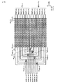
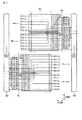
図18は、ドライバの回路例を示している。 FIG. 18 shows a circuit example of the driver.
メモリセルアレイに関し、1ブロック内のワード線の数を4本(4層)とし、ビット線側セレクトゲート線の数を8本(1層)とし、ソース線側セレクトゲート線の数を1本(1層)とする。 Regarding the memory cell array, the number of word lines in one block is 4 (4 layers), the number of bit line side select gate lines is 8 (1 layer), and the number of source line side select gate lines is 1 ( 1 layer).
ドライバ33は、高電圧が印加される転送トランジスタ(高電圧トランジスタ)から構成される。ロウデコーダ35は、アンド回路から構成され、アドレス信号ADDRESSをデコードする。レベルシフタ34は、ドライバ33とロウデコーダ35の間に接続される。
The
BSTON、VRDEC、RDECANDn<0>及びRDECANDn<1>は、転送トランジスタのオン/オフを制御する制御信号であり、SGD<7:0>, CGi<3:0>, CG(i+1)<3:0>, SGSi, SGS(i+1), VRDEC2, SGDSは、転送電圧である。 BSTON, VRDEC, RDECANDn <0> and RDECANDn <1> are control signals for controlling on / off of the transfer transistor, and SGD <7: 0>, CGi <3: 0>, CG (i + 1) < 3: 0>, SGSi, SGS (i + 1), VRDEC2, and SGDS are transfer voltages.
(4) リードディスターブ及びリード手法
A. リードディスターブ
まず、BiCSメモリに特有のリードディスターブについてBiCS-NANDフラッシュメモリを例に説明する。
(4) Read disturb and read method
A. Read disturb
First, read disturb specific to the BiCS memory will be described by taking a BiCS-NAND flash memory as an example.
図19は、3つのブロックを示している。
ブロックBK<i>を選択されたブロックとし、ブロックBK<i-1>, BK<i+1>を非選択のブロックとする。
FIG. 19 shows three blocks.
Block BK <i> is a selected block, and blocks BK <i-1> and BK <i + 1> are unselected blocks.
選択されたブロックBK<i>は、リード対象となるメモリセルを含む選択されたNANDセルユニットNAND-selectを有する。NANDセルユニットNAND-selectは、互いに交差して配置される選択されたビット線BL-selectと選択されたビット線側セレクトゲート線SGD-selectとの交点に位置する。 The selected block BK <i> has a selected NAND cell unit NAND-select including a memory cell to be read. The NAND cell unit NAND-select is located at the intersection of the selected bit line BL-select and the selected bit line side select gate line SGD-select arranged so as to cross each other.
リード時に、選択されたブロックBK<i>内の選択されたワード線WL-selectにはリード電位Vcgrvが与えられ、選択されたブロックBK<i>内の非選択のワード線WL-unselectにはリード電位Vcgrvよりも高い転送電位Vreadが与えられる。リード電位Vcgrvは、メモリセルの閾値状態に応じてそのメモリセルをオン又はオフにする電位であり、転送電位Vreadは、メモリセルの閾値状態によらずそのメモリセルをオンにする電位である。 At the time of reading, the read potential Vcgrv is applied to the selected word line WL-select in the selected block BK <i>, and the unselected word line WL-unselect in the selected block BK <i> is applied. A transfer potential Vread higher than the read potential Vcgrv is applied. The read potential Vcgrv is a potential that turns on or off the memory cell according to the threshold state of the memory cell, and the transfer potential Vread is a potential that turns on the memory cell regardless of the threshold state of the memory cell.
ここで、ブロックBK<i>内のNANDセルユニットは、ワード線を共有するため、ブロックBK<i>内では、選択されたNANDセルユニット以外の非選択のNANDセルユニットにも、リード電位Vcgrv及び転送電位Vreadが印加される。 Here, since the NAND cell units in the block BK <i> share a word line, the read potential Vcgrv is also applied to unselected NAND cell units other than the selected NAND cell unit in the block BK <i>. The transfer potential Vread is applied.
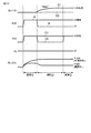
ブロックBK<i>内のリード時の電位関係は、図20に示すようになる。
選択されたワード線WL-selectには、リード電位Vcgrvが印加され、非選択のワード線WL-unselectには、転送電位Vreadが印加される。また、選択されたビット線側セレクトゲート線SGD-selectには、ビット線側セレクトゲートトランジスタをオンにする電位としてVsgd(例えば、約4V)が印加され、非選択のビット線側セレクトゲート線SGD-unselectには、ビット線側セレクトゲートトランジスタをオフにする電位としてVss(例えば、0V)が印加される。さらに、ソース線側セレクトゲート線SGSには、ソース線側セレクトゲートトランジスタをオンにする電位としてVsgs(例えば、約4V)が印加される。
The potential relationship during reading in the block BK <i> is as shown in FIG.
The read potential Vcgrv is applied to the selected word line WL-select, and the transfer potential Vread is applied to the unselected word line WL-unselect. Also, Vsgd (for example, about 4 V) is applied to the selected bit line side select gate line SGD-select as a potential for turning on the bit line side select gate transistor, and the unselected bit line side select gate line SGD -unselect is applied with Vss (for example, 0 V) as a potential for turning off the bit line side select gate transistor. Further, Vsgs (for example, about 4 V) is applied to the source line side select gate line SGS as a potential for turning on the source line side select gate transistor.
選択されたビット線BL-selectは、予め、プリチャージ電位Vpreにプリチャージされているため、選択されたメモリセルMC-selectの閾値状態に応じて選択されたビット線BL-selectの電位が変動する。この変動をセンスアンプにより検出し、選択されたメモリセルMC-selectのデータを判定する。 Since the selected bit line BL-select is precharged to the precharge potential Vpre in advance, the potential of the selected bit line BL-select varies according to the threshold state of the selected memory cell MC-select. To do. This variation is detected by a sense amplifier, and the data of the selected memory cell MC-select is determined.
この時、特に、リード電位Vcgrvが印加されるワード線WL-selectに接続される非選択のメモリセルX1のビット線BL-select側に隣接するメモリセルX2について、リードディスターブが発生し易くなる。 At this time, in particular, read disturb is likely to occur in the memory cell X2 adjacent to the bit line BL-select side of the unselected memory cell X1 connected to the word line WL-select to which the read potential Vcgrv is applied.
B. 従来のリード手法(参考例)
リードディスターブの発生について具体的に説明する。
B. Conventional lead method (reference example)
The generation of read disturb will be specifically described.
図21は、従来のリード手法を示すタイミングチャートである。図22及び図23は、リード時の電位関係を示している。 FIG. 21 is a timing chart showing a conventional read method. 22 and 23 show the potential relationship during reading.
まず、選択されたブロックBK<i>内において、選択されたワード線WL<2>にリード電位Vcgrvを与え、非選択のワード線WL<0>, WL<1>, WL<3>に転送電位Vreadを与える。また、選択されたNANDセルユニットNAND-select1, NAND-select2内のビット線側セレクトゲート線SGDにビット線側セレクトゲートトランジスタをオンにする電位Vsgd(ex. 4V)を与え(実線A)、非選択のNANDセルユニットNAND-unselect内のビット線側セレクトゲート線SGDにビット線側セレクトゲートトランジスタをオフにする電位Vss(ex. 0V)を与える(破線B)。さらに、ソース線SLに接地電位Vssを与える。 First, in the selected block BK <i>, the read potential Vcgrv is applied to the selected word line WL <2> and transferred to the unselected word lines WL <0>, WL <1>, WL <3>. The potential Vread is given. Also, the potential Vsgd (ex. A potential Vss (ex. 0V) for turning off the bit line side select gate transistor is applied to the bit line side select gate line SGD in the selected NAND cell unit NAND-unselect (broken line B). Further, the ground potential Vss is applied to the source line SL.
また、ABL (All Bit Line)センス方式を採用する場合には、図22に示すように、全てのビット線BL<0>, BL<1>にプリチャージ電位Vpreを与え、ソース線側セレクトゲート線SGSにソース線側セレクトゲートトランジスタをオンにする電位Vsgsを与える(図21の実線C1)。これに対し、シールドビット線センス方式を採用する場合には、図23に示すように、選択されたビット線BL<0>にプリチャージ電位Vpreを与え、非選択のビット線BL<1>にシールド電位Vss(ex. 0V)を与え、選択されたソース線側セレクトゲート線SGSにソース線側セレクトゲートトランジスタをオンにする電位Vsgsを与え、非選択のソース線側セレクトゲート線SGSにソース線側セレクトゲートトランジスタをオフにする電位Vssを与えた後にVsgsを与える(図21の破線C2)。 When the ABL (All Bit Line) sensing method is adopted, as shown in FIG. 22, the precharge potential Vpre is applied to all the bit lines BL <0>, BL <1>, and the source line side select gates are applied. A potential Vsgs for turning on the source line side select gate transistor is applied to the line SGS (solid line C1 in FIG. 21). On the other hand, when the shield bit line sensing method is adopted, as shown in FIG. 23, the precharge potential Vpre is applied to the selected bit line BL <0>, and the unselected bit line BL <1> is applied. Apply shield potential Vss (ex. 0V), supply source line side select gate line SGS with potential Vsgs to turn on source line side select gate transistor, and select unselected source line side select gate line SGS with source line After applying the potential Vss for turning off the side select gate transistor, Vsgs is applied (broken line C2 in FIG. 21).
非選択のブロックBK<i-1>, BK<i+1>については、図22及び図23に示すような電位関係にする。 The non-selected blocks BK <i-1> and BK <i + 1> have a potential relationship as shown in FIGS.
この時、選択されたブロックBK<i>内の非選択のNANDセルユニットNAND-unselectは、ビット線側セレクトゲートトランジスタがオフであり、リード時にビット線から切断される。また、非選択のNANDセルユニットNAND-unselect内のリード電位Vcgrvが与えられる非選択のメモリセルX1が高い閾値状態、例えば、2値記憶(“0”/”1”)の”0”状態である場合には、その非選択のメモリセルX1は、リード電位Vcgrvが印加される前後においてオフである。 At this time, the unselected NAND cell unit NAND-unselect in the selected block BK <i> is disconnected from the bit line at the time of reading because the bit line side select gate transistor is off. Further, the non-selected memory cell X1 to which the read potential Vcgrv in the non-selected NAND cell unit NAND-unselect is applied is in a high threshold state, for example, in the “0” state of binary storage (“0” / “1”) In some cases, the non-selected memory cell X1 is off before and after the read potential Vcgrv is applied.
このため、非選択のNANDセルユニットNAND-unselect内のリード電位Vcgrvが与えられるメモリセルX1よりもビット線側に存在するメモリセルX2のチャネルは、フローティング状態であり、かつ、リード電位Vcgrvが印加されたときに容量カップリングによりチャネルブーストされる(Vboost)。 For this reason, the channel of the memory cell X2 existing on the bit line side of the memory cell X1 to which the read potential Vcgrv in the unselected NAND cell unit NAND-unselect is applied is in a floating state and the read potential Vcgrv is applied. When boosted, the channel is boosted by capacitive coupling (Vboost).
一方、BiCSメモリでは、リード時には、非選択のNANDセルユニットNAND-unselect内のリード電位Vcgrvが与えられるメモリセルX1よりもソース線側に存在するメモリセルのチャネルは、ソース線SLから接地電位Vssが転送される。 On the other hand, in the BiCS memory, at the time of reading, the channel of the memory cell existing on the source line side from the memory cell X1 to which the read potential Vcgrv in the unselected NAND cell unit NAND-unselect is applied is connected from the source line SL to the ground potential Vss Is transferred.
従って、非選択のNANDセルユニットNAND-unselect内のリード電位Vcgrvが与えられるメモリセルX1には、ソース及びドレイン間に大きな電位差が発生し、それが原因となり、そのメモリセルX1のソース及びドレイン間にパンチスルーが発生する。 Therefore, in the memory cell X1 to which the read potential Vcgrv in the unselected NAND cell unit NAND-unselect is applied, a large potential difference is generated between the source and the drain, and this is caused by the difference between the source and the drain of the memory cell X1. Punch through occurs.
このパンチスルーに起因してホットキャリアが発生し、このホットキャリアが非選択のNANDセルユニットNAND-unselect内のリード電位Vcgrvが与えられるメモリセルX1よりもビット線BL<0>, BL<1>側に存在するメモリセルX2の電荷蓄積層に注入され、閾値電圧の変動が生じる。 Hot carriers are generated due to the punch-through, and the hot carriers are bit lines BL <0>, BL <1> rather than the memory cell X1 to which the read potential Vcgrv in the unselected NAND cell unit NAND-unselect is applied. It is injected into the charge storage layer of the memory cell X2 existing on the side, and the threshold voltage varies.
図24は、リードディスターブ発生時の状況を示している。
同図(a)は、選択されたメモリセルMC-select1, MC-select2を含むNANDセルユニットを示し、同図(b)は、非選択のメモリセルのみを含むNANDセルユニットを示している。同図(b)において、メモリセルX1, X2は、図22及び図23のメモリセルX1, X2に対応している。
FIG. 24 shows the situation when a read disturb occurs.
FIG. 4A shows a NAND cell unit including selected memory cells MC-select1 and MC-select2, and FIG. 4B shows a NAND cell unit including only non-selected memory cells. In FIG. 2B, memory cells X1 and X2 correspond to the memory cells X1 and X2 in FIGS.
C. 本発明の例に係わるリード手法
上述のリードディスターブを防止するには、リード時に、非選択のセルユニット内のリード電位が与えられるメモリセルのソース及びドレイン間に大きな電位差が発生しないように、動作タイミングを工夫すればよい。
C. Lead method according to an example of the present invention
In order to prevent the above-described read disturb, the operation timing may be devised so that a large potential difference does not occur between the source and drain of the memory cell to which the read potential in the non-selected cell unit is applied at the time of reading.
図25は、本発明の例に係わるリード手法を示すタイミングチャートである。図26及び図27は、リード時の電位関係を示している。 FIG. 25 is a timing chart showing a read method according to an example of the present invention. 26 and 27 show the potential relationship during reading.
・ 期間1
選択されたブロックBK<i>内において、選択されたワード線WL<2>にリード電位Vcgrvを与え、非選択のワード線WL<0>, WL<1>, WL<3>に転送電位Vreadを与える。また、全てのビット線側セレクトゲート線SGDにビット線側セレクトゲートトランジスタをオンにする電位Vsgd(ex. 4V)を与え、全てのソース線側セレクトゲート線SGSにソース線側セレクトゲートトランジスタをオンにする電位Vsgs(ex. 4V)を与える。全てのビット線BL<0>, BL<1>及びソース線SLには接地電位Vssを与える。
・
In the selected block BK <i>, the read potential Vcgrv is applied to the selected word line WL <2>, and the transfer potential Vread is applied to the unselected word lines WL <0>, WL <1>, WL <3>. give. Further, the potential Vsgd (ex. 4V) for turning on the bit line side select gate transistors is applied to all the bit line side select gate lines SGD, and the source line side select gate transistors are turned on to all the source line side select gate lines SGS. Potential Vsgs (ex. 4V) is applied. A ground potential Vss is applied to all the bit lines BL <0>, BL <1> and the source line SL.
ここで、本発明の例に係わるリード手法が従来のリード手法と異なる点は、選択されたブロックBK<i>内の非選択のNANDセルユニットNAND-unselect内のリード電位Vcgrvが印加されるメモリセルX1よりもビット線BL<0>, BL<1>側に存在するメモリセルX2のチャネルに接地電位Vssを与えた状態で、選択されたブロックBK<i>内のワード線WL<0>, WL<1>, WL<2> WL<3>リード電位Vcgrv又は転送電位Vreadを印加していることにある。 Here, the read method according to the example of the present invention is different from the conventional read method in that the read potential Vcgrv in the unselected NAND cell unit NAND-unselect in the selected block BK <i> is applied. The word line WL <0> in the selected block BK <i> with the ground potential Vss applied to the channel of the memory cell X2 existing on the bit line BL <0>, BL <1> side of the cell X1 , WL <1>, WL <2> WL <3> read potential Vcgrv or transfer potential Vread.
この場合、選択されたブロックBK<i>内のワード線WL<0>, WL<1>, WL<2> WL<3>リード電位Vcgrv又は転送電位Vreadを印加したときに、非選択のNANDセルユニットNAND-unselect内のメモリセルX2のチャネルは接地電位Vssに固定された状態にあるため、そのメモリセルX2のチャネルがブーストされることはない。 In this case, unselected NAND when the word line WL <0>, WL <1>, WL <2> WL <3> read potential Vcgrv or transfer potential Vread in the selected block BK <i> is applied. Since the channel of the memory cell X2 in the cell unit NAND-unselect is fixed at the ground potential Vss, the channel of the memory cell X2 is not boosted.
・ 期間2〜3
選択されたNANDセルユニットNAND-select1, NAND-select2内のビット線側セレクトゲート線SGDにビット線側セレクトゲートトランジスタをオンにする電位Vsgd(ex. 4V)を与え(実線A)、非選択のNANDセルユニットNAND-unselect内のビット線側セレクトゲート線SGDにビット線側セレクトゲートトランジスタをオフにする電位Vss(ex. 0V)を与える(破線B)。さらに、ソース線SLに接地電位Vssを与える。
・ Period 2-3
A potential Vsgd (ex. 4V) for turning on the bit line side select gate transistor is applied to the bit line side select gate line SGD in the selected NAND cell unit NAND-select1, NAND-select2 (solid line A), and the non-selected A potential Vss (ex. 0V) for turning off the bit line side select gate transistor is applied to the bit line side select gate line SGD in the NAND cell unit NAND-unselect (dashed line B). Further, the ground potential Vss is applied to the source line SL.
また、ABLセンス方式を採用する場合には、図26に示すように、全てのビット線BL<0>, BL<1>にプリチャージ電位Vpreを与え、ソース線側セレクトゲート線SGSにソース線側セレクトゲートトランジスタをオンにする電位Vsgs(ex. 4V)を与える(図25の実線C1)。これに対し、シールドビット線センス方式を採用する場合には、図27に示すように、選択されたビット線BL<0>にプリチャージ電位Vpreを与え、非選択のビット線BL<1>にシールド電位Vss(ex. 0V)を与え、選択されたソース線側セレクトゲート線SGSにソース線側セレクトゲートトランジスタをオンにする電位Vsgsを与え、非選択のソース線側セレクトゲート線SGSにソース線側セレクトゲートトランジスタをオフにする電位Vssを与えた後にVsgsを与える(図25の破線C2)。 Further, when the ABL sense method is adopted, as shown in FIG. 26, a precharge potential Vpre is applied to all the bit lines BL <0>, BL <1>, and the source line side select gate line SGS is supplied with the source line. A potential Vsgs (ex. 4V) for turning on the side select gate transistor is applied (solid line C1 in FIG. 25). On the other hand, when the shield bit line sensing method is adopted, as shown in FIG. 27, the precharge potential Vpre is applied to the selected bit line BL <0>, and the unselected bit line BL <1> is applied. Apply shield potential Vss (ex. 0V), supply source line side select gate line SGS with potential Vsgs to turn on source line side select gate transistor, and select unselected source line side select gate line SGS with source line After applying the potential Vss for turning off the side select gate transistor, Vsgs is applied (broken line C2 in FIG. 25).
非選択のブロックBK<i-1>, BK<i+1>については、図26及び図27に示すような電位関係にする。 The non-selected blocks BK <i-1> and BK <i + 1> have a potential relationship as shown in FIGS.
この時、選択されたブロックBK<i>内の非選択のNANDセルユニットNAND-unselectは、ビット線側セレクトゲートトランジスタがオフであり、リード時にビット線から切断される。また、非選択のNANDセルユニットNAND-unselect内のリード電位Vcgrvが与えられる非選択のメモリセルX1が高い閾値状態、例えば、2値記憶(“0”/”1”)の”0”状態である場合には、その非選択のメモリセルX1はオフである。 At this time, the unselected NAND cell unit NAND-unselect in the selected block BK <i> is disconnected from the bit line at the time of reading because the bit line side select gate transistor is off. Further, the non-selected memory cell X1 to which the read potential Vcgrv in the non-selected NAND cell unit NAND-unselect is applied is in a high threshold state, for example, in the “0” state of binary storage (“0” / “1”) In some cases, the unselected memory cell X1 is off.
このため、非選択のNANDセルユニットNAND-unselect内のリード電位Vcgrvが与えられるメモリセルX1よりもビット線側に存在するメモリセルX2のチャネルは、フローティング状態である。 Therefore, the channel of the memory cell X2 existing on the bit line side from the memory cell X1 to which the read potential Vcgrv in the unselected NAND cell unit NAND-unselect is applied is in a floating state.
しかし、選択されたブロックBK<i>に対しては、既に、期間1においてリード電位Vcgrv及び転送電位Vreadが与えられているため、メモリセルX2のチャネルが容量カップリングによりチャネルブーストされるということはない。
However, since the read potential Vcgrv and the transfer potential Vread have already been applied to the selected block BK <i> in the
従って、非選択のNANDセルユニットNAND-unselect内において、メモリセルX1よりもソース線側に存在するメモリセルのチャネルにソース線SLから接地電位Vssが転送されても、メモリセルX1のソース及びドレイン間に大きな電位差が発生することはなく、結果として、メモリセルX2の閾値電圧の変動(リードディスターブ)が防止される。 Therefore, in the unselected NAND cell unit NAND-unselect, even if the ground potential Vss is transferred from the source line SL to the channel of the memory cell existing on the source line side from the memory cell X1, the source and drain of the memory cell X1 A large potential difference does not occur between them, and as a result, fluctuations in the threshold voltage of the memory cell X2 (read disturb) are prevented.
図28は、リード電位及び転送電位の印加時の状況を示している。
同図(a)は、選択されたメモリセルMC-select1, MC-select2を含むNANDセルユニットを示し、同図(b)は、非選択のメモリセルのみを含むNANDセルユニットを示している。同図(b)において、メモリセルX1, X2は、図26及び図27のメモリセルX1, X2に対応し、丸数字1〜3は、図25の期間1〜3に対応している。
FIG. 28 shows a situation when a read potential and a transfer potential are applied.
FIG. 4A shows a NAND cell unit including selected memory cells MC-select1 and MC-select2, and FIG. 4B shows a NAND cell unit including only non-selected memory cells. In FIG. 5B, memory cells X1 and X2 correspond to the memory cells X1 and X2 in FIGS. 26 and 27, and
同図(b)から明らかなように、選択されたブロックBK<i>内のワード線WL<0>, WL<1>, WL<2> WL<3>リード電位Vcgrv又は転送電位Vreadを印加したときに、非選択のNANDセルユニットNAND-unselect内のメモリセルX2のチャネルは、接地電位Vssに固定された状態にあるため、そのメモリセルX2のチャネルがブーストされることはない。 As is clear from FIG. 5B, the read potential Vcgrv or the transfer potential Vread is applied to the word lines WL <0>, WL <1>, WL <2> WL <3> in the selected block BK <i>. In this case, since the channel of the memory cell X2 in the unselected NAND cell unit NAND-unselect is fixed to the ground potential Vss, the channel of the memory cell X2 is not boosted.
D. その他
本発明の例に係わるリード手法においては、図25の動作タイミングに限定されることはなく、以下の場合に有効である。
D. Other
The read method according to the example of the present invention is not limited to the operation timing of FIG. 25 and is effective in the following cases.
期間1において、ビット線から、非選択のNANDセルユニット内のリード電位が印加されるメモリセルよりもビット線側に存在するメモリセルのチャネルに接地電位を供給しているが、これに代えて、ソース線から接地電位を供給してもよい。但し、この場合には、期間1において、選択されたワード線にも転送電位Vreadを与える。
In
リード電位Vcgrv又は転送電位Vreadを選択されたブロック内のワード線に印加するタイミングは、選択されたブロック内の非選択のNANDセルユニット内の全てのメモリセルをビット線から切断するタイミングよりも前であればよい。 The timing at which the read potential Vcgrv or the transfer potential Vread is applied to the word line in the selected block is earlier than the timing at which all the memory cells in the unselected NAND cell unit in the selected block are disconnected from the bit line. If it is.
プリチャージ電位Vpreをビット線に印加するタイミングは、選択されたブロック内の非選択のNANDセルユニット内の全てのメモリセルをビット線から切断するタイミングと同じ又はそれよりも後であればよい。 The timing at which the precharge potential Vpre is applied to the bit line may be the same as or later than the timing at which all the memory cells in the unselected NAND cell unit in the selected block are disconnected from the bit line.
(5) まとめ
以上のように、本発明の実施形態によれば、BiCS技術が適用された三次元積層不揮発性半導体メモリのリードディスターブを改善することができる。
(5) Summary As described above, according to the embodiment of the present invention, read disturb of a three-dimensional stacked nonvolatile semiconductor memory to which BiCS technology is applied can be improved.
4. 適用例
本発明の技術は、ビットコストスケーラビリティを実現するため、1つのセルユニットが直列接続された複数のメモリセル(NAND列)から構成されるBiCS-NANDフラッシュメモリに有効であるが、それ以外にも、BiCS技術が適用された三次元積層不揮発性半導体メモリに適用可能である。
4). Application examples
The technology of the present invention is effective for a BiCS-NAND flash memory composed of a plurality of memory cells (NAND columns) in which one cell unit is connected in series in order to realize bit cost scalability. It can be applied to a three-dimensional stacked nonvolatile semiconductor memory to which BiCS technology is applied.
例えば、BiCS-NANDフラッシュメモリ以外の例として、デバイス構造はBiCS-NANDフラッシュメモリと全く同じであるが、1つのセルユニット内の複数のメモリセルのうち、中央の1つのみをメモリセルとして用い、残りはダミーセルとして用いるような不揮発性半導体メモリにも有効である。 For example, as an example other than the BiCS-NAND flash memory, the device structure is exactly the same as that of the BiCS-NAND flash memory, but only one of the plurality of memory cells in one cell unit is used as a memory cell. The remainder is also effective for a nonvolatile semiconductor memory used as a dummy cell.
また、BiCSメモリのメモリセル構造については、電荷蓄積層が絶縁体(例えば、窒化物)から構成されるいわゆるMONOS型が有効であると考えられているが、本発明の例は、これに限られず、電荷蓄積層が導電性ポリシリコンから構成されるフローティングゲート型に適用することも可能である。 As for the memory cell structure of the BiCS memory, a so-called MONOS type in which the charge storage layer is made of an insulator (for example, a nitride) is considered effective, but the example of the present invention is not limited to this. However, the present invention can also be applied to a floating gate type in which the charge storage layer is made of conductive polysilicon.
さらに、1つのメモリセルに記憶させるデータ値については、2値(two-level)であってもよいし、3値(three-level)以上の多値(multi-level)であってもよい。 Furthermore, the data value stored in one memory cell may be a binary (two-level) or a multi-level that is three or more (three-level).
5. むすび
本発明によれば、BiCS技術が適用された三次元積層不揮発性半導体メモリのリードディスターブを改善することができる。
5. Conclusion
According to the present invention, read disturb of a three-dimensional stacked nonvolatile semiconductor memory to which BiCS technology is applied can be improved.
本発明の例は、上述の実施形態に限定されるものではなく、その要旨を逸脱しない範囲で、各構成要素を変形して具体化できる。また、上述の実施形態に開示されている複数の構成要素の適宜な組み合せにより種々の発明を構成できる。例えば、上述の実施形態に開示される全構成要素から幾つかの構成要素を削除してもよいし、異なる実施形態の構成要素を適宜組み合わせてもよい。 The example of the present invention is not limited to the above-described embodiment, and can be embodied by modifying each component without departing from the gist thereof. Various inventions can be configured by appropriately combining a plurality of constituent elements disclosed in the above-described embodiments. For example, some constituent elements may be deleted from all the constituent elements disclosed in the above-described embodiments, or constituent elements of different embodiments may be appropriately combined.
WL<0>, …WL<3>: ワード線、 BL<0>, …BL<m>: ビット線、 SGS: ソース線側セレクトゲート線、 SGD<0>, …SGD<5>: ビット線側セレクトゲート線、 AA: アクティブエリア。 WL <0>,… WL <3>: Word line, BL <0>,… BL <m>: Bit line, SGS: Source line side select gate line, SGD <0>,… SGD <5>: Bit line Side select gate line, AA: Active area.
Claims (5)
前記第一及び第二ブロックは、それぞれ、前記半導体基板上に互いに絶縁されてスタックされる3以上の導電層と、前記3以上の導電層上にこれらとは絶縁されて配置されるビット線と、下端が前記半導体基板に接続され、上端が前記ビット線に接続され、前記3以上の導電層を突き抜ける複数の半導体柱とから構成され、
前記3以上の導電層のうち最上層は、前記第二方向に延びる複数の第一セレクトゲート線から構成され、前記3以上の導電層のうち最下層は、第二セレクトゲート線であり、前記3以上の導電層のうち前記最上層及び前記最下層を除く残りの導電層は、ワード線であり、
前記3以上の導電層のうち前記最上層を除く残りの導電層は、前記第一方向の幅が前記複数の第一セレクトゲート線の前記第一方向の幅よりも広いプレート状を有し、
前記複数の第一セレクトゲート線の各々と前記複数の半導体柱及び前記第二セレクトゲート線と前記複数の半導体柱とによりそれぞれセレクトゲートトランジスタが構成され、前記ワード線と前記複数の半導体柱とによりそれぞれメモリセルが構成され、
前記第一ブロックは、リード対象となるメモリセルを含む選択された第一セルユニット及びリード対象となるメモリセルを含まない非選択の第二セルユニットを有し、前記第二セルユニット内の前記リード電位が印加されるメモリセルよりも前記ビット線側に存在するメモリセルのチャネルに接地電位を与えた状態で前記第一ブロック内の前記ワード線にリード電位又はそれよりも高い転送電位を印加し、この後、前記第二セルユニット内の全てのメモリセルを前記ビット線から切断し、前記ビット線をプリチャージ電位にして、前記第一セルユニット内の前記リード対象となるメモリセルに対してリードを実行し、
前記リード時に、前記第二ブロック内の前記ワード線には前記リード電位及び前記転送電位が印加されない
ことを特徴とする三次元積層不揮発性半導体メモリ。 A memory cell array composed of a semiconductor substrate, first and second blocks arranged side by side in the first direction on the semiconductor substrate, and one end of the memory cell array in a second direction orthogonal to the first direction And a first driver
The first and second blocks each include three or more conductive layers that are insulated and stacked on the semiconductor substrate, and a bit line that is disposed on the three or more conductive layers and insulated from them. A plurality of semiconductor pillars having a lower end connected to the semiconductor substrate, an upper end connected to the bit line, and penetrating the three or more conductive layers;
The uppermost layer of the three or more conductive layers is composed of a plurality of first select gate lines extending in the second direction, and the lowermost layer of the three or more conductive layers is a second select gate line, Of the three or more conductive layers, the remaining conductive layers excluding the uppermost layer and the lowermost layer are word lines,
The remaining conductive layers other than the uppermost layer among the three or more conductive layers have a plate shape in which the width in the first direction is wider than the width in the first direction of the plurality of first select gate lines,
Each of the plurality of first select gate lines, the plurality of semiconductor pillars, the second select gate line, and the plurality of semiconductor pillars respectively constitute a select gate transistor, and the word line and the plurality of semiconductor pillars. Each memory cell is configured,
The first block has a selected first cell unit including a memory cell to be read and a non-selected second cell unit not including a memory cell to be read, and the first block in the second cell unit A read potential or a transfer potential higher than that is applied to the word line in the first block in a state where a ground potential is applied to the channel of the memory cell existing on the bit line side of the memory cell to which the read potential is applied. Thereafter, all the memory cells in the second cell unit are disconnected from the bit line, the bit line is set to a precharge potential, and the memory cell to be read in the first cell unit is Run the lead
The three-dimensional stacked nonvolatile semiconductor memory, wherein the read potential and the transfer potential are not applied to the word line in the second block during the read.
Priority Applications (5)
| Application Number | Priority Date | Filing Date | Title |
|---|---|---|---|
| JP2008112660A JP5259242B2 (en) | 2008-04-23 | 2008-04-23 | Three-dimensional stacked nonvolatile semiconductor memory |
| US12/407,494 US7852676B2 (en) | 2008-04-23 | 2009-03-19 | Three dimensional stacked nonvolatile semiconductor memory |
| US12/953,193 US8107292B2 (en) | 2008-04-23 | 2010-11-23 | Three dimensional stacked nonvolatile semiconductor memory |
| US13/341,123 US20120099377A1 (en) | 2008-04-23 | 2011-12-30 | Three dimensional stacked nonvolatile semiconductor memory |
| US13/738,660 US8582361B2 (en) | 2008-04-23 | 2013-01-10 | Three dimensional stacked nonvolatile semiconductor memory |
Applications Claiming Priority (1)
| Application Number | Priority Date | Filing Date | Title |
|---|---|---|---|
| JP2008112660A JP5259242B2 (en) | 2008-04-23 | 2008-04-23 | Three-dimensional stacked nonvolatile semiconductor memory |
Publications (2)
| Publication Number | Publication Date |
|---|---|
| JP2009266281A JP2009266281A (en) | 2009-11-12 |
| JP5259242B2 true JP5259242B2 (en) | 2013-08-07 |
Family
ID=41214882
Family Applications (1)
| Application Number | Title | Priority Date | Filing Date |
|---|---|---|---|
| JP2008112660A Active JP5259242B2 (en) | 2008-04-23 | 2008-04-23 | Three-dimensional stacked nonvolatile semiconductor memory |
Country Status (2)
| Country | Link |
|---|---|
| US (4) | US7852676B2 (en) |
| JP (1) | JP5259242B2 (en) |
Families Citing this family (122)
| Publication number | Priority date | Publication date | Assignee | Title |
|---|---|---|---|---|
| JP2009266944A (en) * | 2008-04-23 | 2009-11-12 | Toshiba Corp | Three-dimensional stacked nonvolatile semiconductor memory |
| JP2009266946A (en) | 2008-04-23 | 2009-11-12 | Toshiba Corp | Three-dimensional stacked nonvolatile semiconductor memory |
| JP5259242B2 (en) * | 2008-04-23 | 2013-08-07 | 株式会社東芝 | Three-dimensional stacked nonvolatile semiconductor memory |
| JP4530081B2 (en) * | 2008-07-25 | 2010-08-25 | トヨタ自動車株式会社 | Catalyst deterioration diagnosis apparatus and catalyst deterioration diagnosis method for internal combustion engine |
| JP5193796B2 (en) | 2008-10-21 | 2013-05-08 | 株式会社東芝 | Three-dimensional stacked nonvolatile semiconductor memory |
| JP2011040706A (en) * | 2009-07-15 | 2011-02-24 | Toshiba Corp | Nonvolatile semiconductor memory device |
| US8541832B2 (en) | 2009-07-23 | 2013-09-24 | Samsung Electronics Co., Ltd. | Integrated circuit memory devices having vertical transistor arrays therein and methods of forming same |
| KR101525130B1 (en) * | 2009-08-03 | 2015-06-03 | 에스케이하이닉스 주식회사 | Vertical channel type non-volatile memory device and method for fabricating the same |
| KR101624975B1 (en) * | 2009-11-17 | 2016-05-30 | 삼성전자주식회사 | Three dimensional semiconductor memory devices |
| KR101623547B1 (en) * | 2009-12-15 | 2016-05-23 | 삼성전자주식회사 | Method for manufacturing rewriteable three dimensional memory device |
| US9324440B2 (en) | 2010-02-09 | 2016-04-26 | Samsung Electronics Co., Ltd. | Nonvolatile memory devices, operating methods thereof and memory systems including the same |
| KR101691088B1 (en) | 2010-02-17 | 2016-12-29 | 삼성전자주식회사 | Nonvolatile memory device, operating method thereof and memory system including the same |
| KR101658479B1 (en) | 2010-02-09 | 2016-09-21 | 삼성전자주식회사 | Nonvolatile memory device, operating method thereof and memory system including the same |
| KR101691092B1 (en) | 2010-08-26 | 2016-12-30 | 삼성전자주식회사 | Nonvolatile memory device, operating method thereof and memory system including the same |
| US9378831B2 (en) | 2010-02-09 | 2016-06-28 | Samsung Electronics Co., Ltd. | Nonvolatile memory devices, operating methods thereof and memory systems including the same |
| US8923060B2 (en) | 2010-02-17 | 2014-12-30 | Samsung Electronics Co., Ltd. | Nonvolatile memory devices and operating methods thereof |
| US8908431B2 (en) | 2010-02-17 | 2014-12-09 | Samsung Electronics Co., Ltd. | Control method of nonvolatile memory device |
| JP5788183B2 (en) | 2010-02-17 | 2015-09-30 | 三星電子株式会社Samsung Electronics Co.,Ltd. | Nonvolatile memory device, method of operating the same, and memory system including the same |
| JP2011170956A (en) * | 2010-02-18 | 2011-09-01 | Samsung Electronics Co Ltd | Nonvolatile memory device, programming method thereof and memory system including the same |
| US8553466B2 (en) * | 2010-03-04 | 2013-10-08 | Samsung Electronics Co., Ltd. | Non-volatile memory device, erasing method thereof, and memory system including the same |
| US8792282B2 (en) | 2010-03-04 | 2014-07-29 | Samsung Electronics Co., Ltd. | Nonvolatile memory devices, memory systems and computing systems |
| KR20110104317A (en) * | 2010-03-16 | 2011-09-22 | 삼성전자주식회사 | Nonvolatile Memory Device with Vertical Channel Structure |
| US8823072B2 (en) | 2010-04-15 | 2014-09-02 | Samsung Electronics Co., Ltd. | Floating gate type nonvolatile memory device and related methods of manufacture and operation |
| KR20120003351A (en) | 2010-07-02 | 2012-01-10 | 삼성전자주식회사 | 3D nonvolatile memory device and its operation method |
| US8446767B2 (en) * | 2010-07-02 | 2013-05-21 | Micron Technology, Inc. | Memories and their formation |
| US8570808B2 (en) | 2010-08-09 | 2013-10-29 | Samsung Electronics Co., Ltd. | Nonvolatile memory device with 3D memory cell array |
| KR101763420B1 (en) | 2010-09-16 | 2017-08-01 | 삼성전자주식회사 | Therr dimensional semiconductor memory devices and methods of fabricating the same |
| KR101686590B1 (en) | 2010-09-20 | 2016-12-14 | 삼성전자주식회사 | Flash memory system and wl interleaving method thereof |
| CN103119656A (en) | 2010-09-24 | 2013-05-22 | 株式会社东芝 | Nonvolatile semiconductor memory device |
| KR101825539B1 (en) | 2010-10-05 | 2018-03-22 | 삼성전자주식회사 | Three Dimensional Semiconductor Memory Device And Method Of Fabricating The Same |
| KR101762828B1 (en) | 2011-04-05 | 2017-07-31 | 삼성전자주식회사 | Nonvolatile memory device and operating method of nonvolatile memory device |
| US8860117B2 (en) | 2011-04-28 | 2014-10-14 | Micron Technology, Inc. | Semiconductor apparatus with multiple tiers of memory cells with peripheral transistors, and methods |
| KR101855324B1 (en) * | 2011-05-04 | 2018-05-09 | 삼성전자주식회사 | Three dimmensional semiconductor memory deivces and methods of fabricating the same |
| JP2013004123A (en) | 2011-06-14 | 2013-01-07 | Toshiba Corp | Nonvolatile semiconductor memory device |
| JP2013012553A (en) | 2011-06-28 | 2013-01-17 | Toshiba Corp | Semiconductor storage device |
| KR20130010641A (en) * | 2011-07-19 | 2013-01-29 | 삼성전자주식회사 | Semiconductor device and method of fabricating the same |
| US8508999B2 (en) | 2011-09-29 | 2013-08-13 | Intel Corporation | Vertical NAND memory |
| US9076544B2 (en) | 2011-11-18 | 2015-07-07 | Sandisk Technologies Inc. | Operation for non-volatile storage system with shared bit lines |
| US8917557B2 (en) | 2011-12-15 | 2014-12-23 | Kabushiki Kaisha Toshiba | Nonvolatile semiconductor memory device |
| US8670285B2 (en) | 2012-02-02 | 2014-03-11 | Sandisk Technologies Inc. | Reducing weak-erase type read disturb in 3D non-volatile memory |
| JP2013254537A (en) | 2012-06-06 | 2013-12-19 | Toshiba Corp | Semiconductor memory and controller |
| US8964474B2 (en) * | 2012-06-15 | 2015-02-24 | Micron Technology, Inc. | Architecture for 3-D NAND memory |
| JP5814867B2 (en) | 2012-06-27 | 2015-11-17 | 株式会社東芝 | Semiconductor memory device |
| US8908444B2 (en) | 2012-08-13 | 2014-12-09 | Sandisk Technologies Inc. | Erase for 3D non-volatile memory with sequential selection of word lines |
| JP2014063555A (en) | 2012-09-24 | 2014-04-10 | Toshiba Corp | Nonvolatile semiconductor memory device and control method of the same |
| US8958244B2 (en) | 2012-10-16 | 2015-02-17 | Conversant Intellectual Property Management Inc. | Split block decoder for a nonvolatile memory device |
| US9704580B2 (en) | 2012-10-22 | 2017-07-11 | Conversant Intellectual Property Management Inc. | Integrated erase voltage path for multiple cell substrates in nonvolatile memory devices |
| US8988937B2 (en) | 2012-10-24 | 2015-03-24 | Sandisk Technologies Inc. | Pre-charge during programming for 3D memory using gate-induced drain leakage |
| KR102015906B1 (en) | 2012-11-12 | 2019-08-29 | 삼성전자주식회사 | Memory system comprising nonvolatile memory device and read method tererof |
| US9466382B2 (en) | 2012-11-14 | 2016-10-11 | Sandisk Technologies Llc | Compensation for sub-block erase |
| US9030879B2 (en) | 2012-11-15 | 2015-05-12 | Conversant Intellectual Property Management Incorporated | Method and system for programming non-volatile memory with junctionless cells |
| US9171620B2 (en) | 2012-11-29 | 2015-10-27 | Sandisk Technologies Inc. | Weighted read scrub for nonvolatile memory |
| US10403766B2 (en) | 2012-12-04 | 2019-09-03 | Conversant Intellectual Property Management Inc. | NAND flash memory with vertical cell stack structure and method for manufacturing same |
| US8988941B2 (en) | 2012-12-18 | 2015-03-24 | SanDisk Tehcnologies Inc. | Select transistor tuning |
| US9007834B2 (en) | 2013-01-10 | 2015-04-14 | Conversant Intellectual Property Management Inc. | Nonvolatile memory with split substrate select gates and hierarchical bitline configuration |
| US9098205B2 (en) | 2013-01-30 | 2015-08-04 | Sandisk Technologies Inc. | Data randomization in 3-D memory |
| KR102067755B1 (en) | 2013-02-12 | 2020-01-17 | 삼성전자주식회사 | Non-volatile memory device and control method thereof |
| KR102081749B1 (en) * | 2013-02-20 | 2020-02-26 | 삼성전자주식회사 | Memory system and programming method thereof |
| KR102102233B1 (en) | 2013-02-22 | 2020-04-21 | 삼성전자주식회사 | Memory system and reading method thereof |
| KR102160290B1 (en) * | 2013-02-28 | 2020-09-25 | 삼성전자주식회사 | Nonvolatile memory and reading method of nonvolatile memory |
| US11222697B2 (en) | 2013-02-28 | 2022-01-11 | Samsung Electronics Co., Ltd. | Three-dimensional nonvolatile memory and method of performing read operation in the nonvolatile memory |
| US9349452B2 (en) | 2013-03-07 | 2016-05-24 | Sandisk Technologies Inc. | Hybrid non-volatile memory cells for shared bit line |
| US9165656B2 (en) * | 2013-03-11 | 2015-10-20 | Sandisk Technologies Inc. | Non-volatile storage with shared bit lines and flat memory cells |
| US9025382B2 (en) | 2013-03-14 | 2015-05-05 | Conversant Intellectual Property Management Inc. | Lithography-friendly local read circuit for NAND flash memory devices and manufacturing method thereof |
| US9202931B2 (en) | 2013-03-14 | 2015-12-01 | Conversant Intellectual Property Management Inc. | Structure and method for manufacture of memory device with thin silicon body |
| US9214235B2 (en) | 2013-04-16 | 2015-12-15 | Conversant Intellectual Property Management Inc. | U-shaped common-body type cell string |
| JP2014235757A (en) * | 2013-05-30 | 2014-12-15 | 株式会社東芝 | controller |
| US9218890B2 (en) | 2013-06-03 | 2015-12-22 | Sandisk Technologies Inc. | Adaptive operation of three dimensional memory |
| US9230656B2 (en) | 2013-06-26 | 2016-01-05 | Sandisk Technologies Inc. | System for maintaining back gate threshold voltage in three dimensional NAND memory |
| KR102127416B1 (en) | 2013-06-27 | 2020-06-26 | 삼성전자주식회사 | Nonvolatile memory device, memory system having the same, and reading method thereof |
| KR102058664B1 (en) | 2013-08-29 | 2019-12-23 | 삼성전자주식회사 | Nonvolatile memroy device and operating method for the same |
| US9142324B2 (en) | 2013-09-03 | 2015-09-22 | Sandisk Technologies Inc. | Bad block reconfiguration in nonvolatile memory |
| JP2015056642A (en) * | 2013-09-13 | 2015-03-23 | 株式会社東芝 | Semiconductor memory device |
| KR102242022B1 (en) | 2013-09-16 | 2021-04-21 | 삼성전자주식회사 | Nonvolatile memory device and program method using thereof |
| US9240238B2 (en) | 2013-09-20 | 2016-01-19 | Sandisk Technologies Inc. | Back gate operation with elevated threshold voltage |
| US20150121156A1 (en) | 2013-10-28 | 2015-04-30 | Sandisk Technologies Inc. | Block Structure Profiling in Three Dimensional Memory |
| US9236394B2 (en) | 2013-11-08 | 2016-01-12 | Conversant Intellectual Property Management Inc. | Three dimensional nonvolatile memory cell structure with upper body connection |
| JP2015097245A (en) * | 2013-11-15 | 2015-05-21 | 株式会社東芝 | Nonvolatile semiconductor storage device and memory system |
| KR102161814B1 (en) * | 2013-11-19 | 2020-10-06 | 삼성전자주식회사 | Vertical memory devices and methods of manufacturing the same |
| KR102150969B1 (en) * | 2013-12-05 | 2020-10-26 | 삼성전자주식회사 | Semiconductor device and method of manufacturing the same |
| US9218886B2 (en) | 2013-12-10 | 2015-12-22 | SanDisk Technologies, Inc. | String dependent parameter setup |
| US9312017B2 (en) | 2014-01-15 | 2016-04-12 | Apple Inc. | Storage in charge-trap memory structures using additional electrically-charged regions |
| KR102116668B1 (en) | 2014-02-04 | 2020-05-29 | 삼성전자주식회사 | Nonvolatile memory device and operating method of nonvolatile memory device |
| US9230689B2 (en) | 2014-03-17 | 2016-01-05 | Sandisk Technologies Inc. | Finding read disturbs on non-volatile memories |
| KR102116674B1 (en) | 2014-03-21 | 2020-06-08 | 삼성전자주식회사 | Nonvolatile memory device and storage device having the same and operation method thereof |
| US9887939B2 (en) | 2015-03-11 | 2018-02-06 | International Business Machines Corporation | Transmitting multi-destination packets in overlay networks |
| KR102188538B1 (en) | 2014-04-21 | 2020-12-09 | 삼성전자주식회사 | Semiconductor Memory Device And Method Of Fabricating The Same |
| KR102248267B1 (en) | 2014-04-30 | 2021-05-07 | 삼성전자주식회사 | Nonvolatile memory device, storage device having the same, and operation and read methods thereof |
| US8918577B1 (en) | 2014-06-13 | 2014-12-23 | Sandisk Technologies Inc. | Three dimensional nonvolatile memory with variable block capacity |
| KR102273185B1 (en) | 2014-07-09 | 2021-07-06 | 삼성전자주식회사 | Nonvolatle memory device, storage device having the same and operation method thereof |
| US9286994B1 (en) | 2015-01-26 | 2016-03-15 | Sandisk Technologies Inc. | Method of reducing hot electron injection type of read disturb in dummy memory cells |
| JP2016170834A (en) | 2015-03-12 | 2016-09-23 | 株式会社東芝 | Semiconductor memory device |
| US9412463B1 (en) | 2015-06-02 | 2016-08-09 | Sandisk Technologies Llc | Reducing hot electron injection type of read disturb in 3D non-volatile memory for edge word lines |
| US9336892B1 (en) | 2015-06-02 | 2016-05-10 | Sandisk Technologies Inc. | Reducing hot electron injection type of read disturb in 3D non-volatile memory |
| JP6538496B2 (en) | 2015-09-11 | 2019-07-03 | 東芝メモリ株式会社 | Memory system |
| US9691473B2 (en) | 2015-09-22 | 2017-06-27 | Sandisk Technologies Llc | Adaptive operation of 3D memory |
| US9401216B1 (en) | 2015-09-22 | 2016-07-26 | Sandisk Technologies Llc | Adaptive operation of 3D NAND memory |
| US10248927B2 (en) | 2015-10-22 | 2019-04-02 | Rakesh Holdings, LLC | Multifunctional self-service shipping and mail processing system |
| US9583503B1 (en) * | 2015-12-11 | 2017-02-28 | Macronix International Co., Ltd. | Three-dimensional semiconductor device and method of manufacturing the same |
| US10373970B2 (en) | 2016-03-02 | 2019-08-06 | Micron Technology, Inc. | Semiconductor device structures including staircase structures, and related methods and electronic systems |
| JP6581019B2 (en) | 2016-03-02 | 2019-09-25 | 東芝メモリ株式会社 | Semiconductor memory device |
| JP2017168164A (en) | 2016-03-15 | 2017-09-21 | 東芝メモリ株式会社 | Memory device |
| US9905514B2 (en) | 2016-04-11 | 2018-02-27 | Micron Technology, Inc. | Semiconductor device structures including staircase structures, and related methods and electronic systems |
| US9679650B1 (en) | 2016-05-06 | 2017-06-13 | Micron Technology, Inc. | 3D NAND memory Z-decoder |
| US9747992B1 (en) | 2016-06-03 | 2017-08-29 | Sandisk Technologies Llc | Non-volatile memory with customized control of injection type of disturb during read operations |
| US10026487B2 (en) | 2016-06-03 | 2018-07-17 | Sandisk Technologies Llc | Non-volatile memory with customized control of injection type of disturb during program verify for improved program performance |
| KR102633029B1 (en) | 2016-08-22 | 2024-02-06 | 삼성전자주식회사 | Nonvolatile memory device, storage device including nonvolatile memory device and reading method of nonvolatile memory device |
| JP6545649B2 (en) * | 2016-09-16 | 2019-07-17 | 東芝メモリ株式会社 | Memory device |
| US10504838B2 (en) | 2016-09-21 | 2019-12-10 | Micron Technology, Inc. | Methods of forming a semiconductor device structure including a stair step structure |
| US10861870B2 (en) * | 2016-09-29 | 2020-12-08 | Intel Corporation | Inverted staircase contact for density improvement to 3D stacked devices |
| KR102579879B1 (en) | 2016-11-14 | 2023-09-18 | 삼성전자주식회사 | Nonvolatile memory devices and method of reading the same |
| JP2018148071A (en) | 2017-03-07 | 2018-09-20 | 東芝メモリ株式会社 | Storage device |
| US10170188B1 (en) | 2017-08-31 | 2019-01-01 | Micron Technology, Inc. | 3D memory device including shared select gate connections between memory blocks |
| US10210941B1 (en) | 2018-01-24 | 2019-02-19 | Sandisk Technologies Llc | Reducing injection type of read disturb in a cold read of a memory device |
| CN113169176B (en) * | 2018-12-20 | 2025-07-25 | 应用材料公司 | Memory cell fabrication for 3D NAND applications |
| CN110021309B (en) * | 2019-03-26 | 2020-10-09 | 上海华力集成电路制造有限公司 | NAND type ROM |
| US10832778B1 (en) * | 2019-06-28 | 2020-11-10 | Sandisk Technologies Llc | Negative voltage wordline methods and systems |
| US10847526B1 (en) * | 2019-07-26 | 2020-11-24 | Micron Technology, Inc. | Microelectronic devices including staircase structures, and related memory devices and electronic systems |
| US11450381B2 (en) | 2019-08-21 | 2022-09-20 | Micron Technology, Inc. | Multi-deck memory device including buffer circuitry under array |
| US11495530B2 (en) | 2020-05-01 | 2022-11-08 | Micron Technology, Inc. | Microelectronic devices including stadium structures, and related methods, memory devices, and electronic systems |
| CN115172379A (en) * | 2021-04-21 | 2022-10-11 | 长江存储科技有限责任公司 | Three-dimensional memory and preparation method thereof |
| JP2023039082A (en) | 2021-09-08 | 2023-03-20 | キオクシア株式会社 | semiconductor storage device |
Family Cites Families (22)
| Publication number | Priority date | Publication date | Assignee | Title |
|---|---|---|---|---|
| JP3651689B2 (en) | 1993-05-28 | 2005-05-25 | 株式会社東芝 | NAND type nonvolatile semiconductor memory device and manufacturing method thereof |
| KR960008823B1 (en) * | 1993-11-30 | 1996-07-05 | Samsung Electronics Co Ltd | Non-volatile semiconductor memory device |
| JP3789977B2 (en) | 1996-05-10 | 2006-06-28 | 株式会社ルネサステクノロジ | Nonvolatile semiconductor memory device |
| JP3344331B2 (en) | 1998-09-30 | 2002-11-11 | 日本電気株式会社 | Nonvolatile semiconductor memory device |
| CN1691331A (en) * | 1999-02-01 | 2005-11-02 | 株式会社日立制作所 | Semiconductor integrated circuit device |
| EP1609154B1 (en) | 2003-03-18 | 2013-12-25 | Kabushiki Kaisha Toshiba | Phase change memory device |
| JP2004319577A (en) | 2003-04-11 | 2004-11-11 | Dainippon Printing Co Ltd | Resin-sealed semiconductor device, method of manufacturing the same, and laminated resin-sealed semiconductor device |
| KR20060001196A (en) | 2004-06-30 | 2006-01-06 | 주식회사 하이닉스반도체 | Device Separator Formation Method of Semiconductor Device |
| US7091890B1 (en) * | 2004-08-17 | 2006-08-15 | Xilinx, Inc. | Multi-purpose source synchronous interface circuitry |
| KR100674952B1 (en) | 2005-02-05 | 2007-01-26 | 삼성전자주식회사 | 3D flash memory device and manufacturing method thereof |
| JP5016832B2 (en) * | 2006-03-27 | 2012-09-05 | 株式会社東芝 | Nonvolatile semiconductor memory device and manufacturing method thereof |
| JP5100080B2 (en) | 2006-10-17 | 2012-12-19 | 株式会社東芝 | Nonvolatile semiconductor memory device and manufacturing method thereof |
| KR20090002636A (en) * | 2007-07-02 | 2009-01-09 | 삼성전자주식회사 | Nonvolatile Memory Device and Erasing Method thereof |
| KR101301140B1 (en) * | 2007-07-13 | 2013-09-03 | 삼성전자주식회사 | Nonvolatile semiconductor memory devices for preventing read disturbance and read method thereof |
| JP5283960B2 (en) * | 2008-04-23 | 2013-09-04 | 株式会社東芝 | Three-dimensional stacked nonvolatile semiconductor memory |
| JP5072696B2 (en) * | 2008-04-23 | 2012-11-14 | 株式会社東芝 | Three-dimensional stacked nonvolatile semiconductor memory |
| JP2009266944A (en) * | 2008-04-23 | 2009-11-12 | Toshiba Corp | Three-dimensional stacked nonvolatile semiconductor memory |
| JP5259242B2 (en) * | 2008-04-23 | 2013-08-07 | 株式会社東芝 | Three-dimensional stacked nonvolatile semiconductor memory |
| JP2009266946A (en) * | 2008-04-23 | 2009-11-12 | Toshiba Corp | Three-dimensional stacked nonvolatile semiconductor memory |
| US8120959B2 (en) * | 2008-05-30 | 2012-02-21 | Aplus Flash Technology, Inc. | NAND string based NAND/NOR flash memory cell, array, and memory device having parallel bit lines and source lines, having a programmable select gating transistor, and circuits and methods for operating same |
| JP5193796B2 (en) * | 2008-10-21 | 2013-05-08 | 株式会社東芝 | Three-dimensional stacked nonvolatile semiconductor memory |
| JP2010134983A (en) * | 2008-12-03 | 2010-06-17 | Toshiba Corp | Depletion type NAND flash memory |
-
2008
- 2008-04-23 JP JP2008112660A patent/JP5259242B2/en active Active
-
2009
- 2009-03-19 US US12/407,494 patent/US7852676B2/en active Active
-
2010
- 2010-11-23 US US12/953,193 patent/US8107292B2/en active Active
-
2011
- 2011-12-30 US US13/341,123 patent/US20120099377A1/en not_active Abandoned
-
2013
- 2013-01-10 US US13/738,660 patent/US8582361B2/en active Active
Also Published As
| Publication number | Publication date |
|---|---|
| US8582361B2 (en) | 2013-11-12 |
| US20110063913A1 (en) | 2011-03-17 |
| US7852676B2 (en) | 2010-12-14 |
| JP2009266281A (en) | 2009-11-12 |
| US8107292B2 (en) | 2012-01-31 |
| US20130121077A1 (en) | 2013-05-16 |
| US20120099377A1 (en) | 2012-04-26 |
| US20090268524A1 (en) | 2009-10-29 |
Similar Documents
| Publication | Publication Date | Title |
|---|---|---|
| JP5259242B2 (en) | Three-dimensional stacked nonvolatile semiconductor memory | |
| US12183400B2 (en) | Three dimensional stacked nonvolatile semiconductor memory having a controller configured to execute a program operation on memory cells | |
| JP5072696B2 (en) | Three-dimensional stacked nonvolatile semiconductor memory | |
| JP5283960B2 (en) | Three-dimensional stacked nonvolatile semiconductor memory | |
| KR101059026B1 (en) | 3-D stacked nonvolatile semiconductor memory | |
| US8203882B2 (en) | Non-volatile semiconductor storage device | |
| US8107286B2 (en) | Three-dimensional nonvolatile semiconductor memory device for curbing a leak current and method of data read therein | |
| US10991713B2 (en) | Semiconductor memory device | |
| US8760925B2 (en) | Non-volatile semiconductor memory device | |
| JP2012204684A (en) | Nonvolatile semiconductor memory device | |
| JP2010098067A (en) | Semiconductor device | |
| JP2019117894A (en) | Semiconductor storage device |
Legal Events
| Date | Code | Title | Description |
|---|---|---|---|
| A621 | Written request for application examination |
Free format text: JAPANESE INTERMEDIATE CODE: A621 Effective date: 20100802 |
|
| A977 | Report on retrieval |
Free format text: JAPANESE INTERMEDIATE CODE: A971007 Effective date: 20130321 |
|
| TRDD | Decision of grant or rejection written | ||
| A01 | Written decision to grant a patent or to grant a registration (utility model) |
Free format text: JAPANESE INTERMEDIATE CODE: A01 Effective date: 20130402 |
|
| A61 | First payment of annual fees (during grant procedure) |
Free format text: JAPANESE INTERMEDIATE CODE: A61 Effective date: 20130424 |
|
| FPAY | Renewal fee payment (event date is renewal date of database) |
Free format text: PAYMENT UNTIL: 20160502 Year of fee payment: 3 |
|
| R151 | Written notification of patent or utility model registration |
Ref document number: 5259242 Country of ref document: JP Free format text: JAPANESE INTERMEDIATE CODE: R151 |
|
| S111 | Request for change of ownership or part of ownership |
Free format text: JAPANESE INTERMEDIATE CODE: R313111 |
|
| R350 | Written notification of registration of transfer |
Free format text: JAPANESE INTERMEDIATE CODE: R350 |
|
| S111 | Request for change of ownership or part of ownership |
Free format text: JAPANESE INTERMEDIATE CODE: R313111 |
|
| R350 | Written notification of registration of transfer |
Free format text: JAPANESE INTERMEDIATE CODE: R350 |