JP5259107B2 - Multilayer ceramic electronic component and manufacturing method thereof - Google Patents
Multilayer ceramic electronic component and manufacturing method thereof Download PDFInfo
- Publication number
- JP5259107B2 JP5259107B2 JP2007075221A JP2007075221A JP5259107B2 JP 5259107 B2 JP5259107 B2 JP 5259107B2 JP 2007075221 A JP2007075221 A JP 2007075221A JP 2007075221 A JP2007075221 A JP 2007075221A JP 5259107 B2 JP5259107 B2 JP 5259107B2
- Authority
- JP
- Japan
- Prior art keywords
- ceramic
- layer
- ceramic laminate
- electrode
- pair
- Prior art date
- Legal status (The legal status is an assumption and is not a legal conclusion. Google has not performed a legal analysis and makes no representation as to the accuracy of the status listed.)
- Expired - Fee Related
Links
- 239000000919 ceramic Substances 0.000 title claims description 199
- 238000004519 manufacturing process Methods 0.000 title claims description 43
- 239000010410 layer Substances 0.000 claims description 128
- 239000004020 conductor Substances 0.000 claims description 83
- 238000007747 plating Methods 0.000 claims description 62
- 238000000605 extraction Methods 0.000 claims description 57
- 238000000034 method Methods 0.000 claims description 49
- XLYOFNOQVPJJNP-UHFFFAOYSA-N water Substances O XLYOFNOQVPJJNP-UHFFFAOYSA-N 0.000 claims description 45
- 239000011247 coating layer Substances 0.000 claims description 43
- 239000005871 repellent Substances 0.000 claims description 28
- PCHJSUWPFVWCPO-UHFFFAOYSA-N gold Chemical compound [Au] PCHJSUWPFVWCPO-UHFFFAOYSA-N 0.000 claims description 15
- 239000010931 gold Substances 0.000 claims description 15
- 229910052737 gold Inorganic materials 0.000 claims description 15
- 239000000463 material Substances 0.000 claims description 13
- 125000003396 thiol group Chemical class [H]S* 0.000 claims description 7
- 238000005520 cutting process Methods 0.000 claims description 3
- 239000003985 ceramic capacitor Substances 0.000 description 42
- 239000010408 film Substances 0.000 description 42
- 239000011248 coating agent Substances 0.000 description 8
- 238000000576 coating method Methods 0.000 description 8
- 230000002940 repellent Effects 0.000 description 6
- 239000002002 slurry Substances 0.000 description 6
- YCKRFDGAMUMZLT-UHFFFAOYSA-N Fluorine atom Chemical compound [F] YCKRFDGAMUMZLT-UHFFFAOYSA-N 0.000 description 4
- 229910052731 fluorine Inorganic materials 0.000 description 4
- 239000011737 fluorine Substances 0.000 description 4
- 238000003475 lamination Methods 0.000 description 4
- 238000012986 modification Methods 0.000 description 4
- 230000004048 modification Effects 0.000 description 4
- 239000011347 resin Substances 0.000 description 4
- 229920005989 resin Polymers 0.000 description 4
- 238000010030 laminating Methods 0.000 description 3
- 238000000059 patterning Methods 0.000 description 3
- 229920000642 polymer Polymers 0.000 description 3
- JRPBQTZRNDNNOP-UHFFFAOYSA-N barium titanate Chemical compound [Ba+2].[Ba+2].[O-][Ti]([O-])([O-])[O-] JRPBQTZRNDNNOP-UHFFFAOYSA-N 0.000 description 2
- 229910002113 barium titanate Inorganic materials 0.000 description 2
- 239000002131 composite material Substances 0.000 description 2
- 238000010586 diagram Methods 0.000 description 2
- 238000009413 insulation Methods 0.000 description 2
- 229920001343 polytetrafluoroethylene Polymers 0.000 description 2
- 239000004810 polytetrafluoroethylene Substances 0.000 description 2
- 239000002904 solvent Substances 0.000 description 2
- 239000000654 additive Substances 0.000 description 1
- 230000000996 additive effect Effects 0.000 description 1
- 239000000470 constituent Substances 0.000 description 1
- 238000000151 deposition Methods 0.000 description 1
- 239000002003 electrode paste Substances 0.000 description 1
- 239000000839 emulsion Substances 0.000 description 1
- 230000007613 environmental effect Effects 0.000 description 1
- 239000002184 metal Substances 0.000 description 1
- 229910052751 metal Inorganic materials 0.000 description 1
- 229910052759 nickel Inorganic materials 0.000 description 1
- -1 polytetrafluoroethylene Polymers 0.000 description 1
- 239000002994 raw material Substances 0.000 description 1
- 230000001846 repelling effect Effects 0.000 description 1
- 238000007789 sealing Methods 0.000 description 1
- 239000007787 solid Substances 0.000 description 1
- 239000010409 thin film Substances 0.000 description 1
Images


Landscapes
- Fixed Capacitors And Capacitor Manufacturing Machines (AREA)
- Ceramic Capacitors (AREA)
Description
本願発明は、積層セラミック電子部品及びその製造方法に関し、詳しくは、セラミック積層体中に、複数の導体層がセラミック層を介して積層され、かつ、複数の導体層が交互に、セラミック積層体の側面の一対の領域に配設された一対の外部電極のいずれか一方に、電気的に接続された構造を有する積層セラミック電子部品およびその製造方法に関する。 The present invention relates to a multilayer ceramic electronic component and a method for manufacturing the same, and more specifically, in a ceramic laminate, a plurality of conductor layers are laminated via ceramic layers, and a plurality of conductor layers are alternately arranged. The present invention relates to a multilayer ceramic electronic component having a structure electrically connected to either one of a pair of external electrodes disposed in a pair of side regions, and a method for manufacturing the same.
近年、積層セラミックコンデンサは種々の用途に広く用いられており、電子機器の小型、高性能化にともない、積層セラミックコンデンサの小型大容量化への要求も大きくなっている。 In recent years, monolithic ceramic capacitors have been widely used for various applications, and the demand for miniaturization and large capacity of monolithic ceramic capacitors has increased as electronic devices have become smaller and higher performance.
このような状況下、小型大容量化のため、内部電極を薄膜形成法により形成して、意図する所定のパターンの内部電極を有する積層セラミックコンデンサを製造する方法が提案されている(特許文献1)。 Under such circumstances, in order to reduce the size and increase the capacity, there has been proposed a method of manufacturing a multilayer ceramic capacitor having internal electrodes of a predetermined pattern intended by forming internal electrodes by a thin film forming method (Patent Document 1). ).
また、内部電極層をパターン化せず、セラミックグリーンシートの表面に全面電極として形成し、この内部電極層を備えたセラミックグリーンシート(誘電体層)を積層した後、全面電極の不要部分を除去してパターン化し、その後、内部電極と導通するように外部電極を形成するようにした積層セラミックコンデンサの製造方法が提案されている(特許文献2)。 Also, the internal electrode layer is not patterned and formed as a full surface electrode on the surface of the ceramic green sheet. After the ceramic green sheet (dielectric layer) having this internal electrode layer is laminated, unnecessary portions of the full surface electrode are removed. A method for manufacturing a multilayer ceramic capacitor in which an external electrode is formed so as to be patterned and then electrically connected to the internal electrode has been proposed (Patent Document 2).
しかしながら、上記特許文献1の方法の場合、規格寸法に合わせて積層セラミック電子部品を製造しようとすると、内部電極の重なり面積(積層セラミックコンデンサの場合における容量取得に寄与する面積)を十分に確保することが困難になり、大容量化が妨げられるという問題点がある。これは、内部電極の印刷精度、積層時の変形、マザー積層体を切断する際の直線性などを考慮して加工マージンを決定する必要があり、セラミック積層体の平面面積よりも内部電極の寸法を小さくしなければならないことによる。
However, in the case of the method disclosed in
また、上記特許文献2の方法の場合、内部電極層を全面電極としているので、特許文献1のように内部電極の周囲にマージンを確保するために内部電極をパターン化することに伴う、製品寸法に対して内部電極の平面面積が小さくなるという問題点は低減できるが、積層後に内部電極の不要部分を除去して絶縁性を確保するようにしているので、十分な絶縁性を確保できる程度にまで内部電極層を除去するのに時間がかかり、生産性が低いという問題点がある。
本願発明は、上記課題を解決するものであり、製品寸法に対して、内部電極の面積を大きくとることが可能で、例えば積層セラミックコンデンサの場合、小型大容量化を図ることができ、しかも、内部電極の不要部を除去する必要がなく、効率よく小型高特性の積層セラミック電子部品を製造することが可能な積層セラミック電子部品の製造方法および該製造方法により製造することが可能な小型高特性の積層セラミック電子部品を提供することを目的とする。 The invention of the present application solves the above-mentioned problems, and it is possible to increase the area of the internal electrode with respect to the product dimensions. For example, in the case of a multilayer ceramic capacitor, the size and capacity can be increased, There is no need to remove unnecessary portions of the internal electrode, and a method for manufacturing a multilayer ceramic electronic component capable of efficiently manufacturing a small and high characteristic multilayer ceramic electronic component, and a small and high property capable of being manufactured by the manufacturing method. An object of the present invention is to provide a multilayer ceramic electronic component.
上記課題を解決するために、本願発明の積層セラミック電子部品の製造方法は、
セラミック積層体中に、複数の導体層がセラミック層を介して積層され、かつ、前記複数の導体層が交互に、セラミック積層体の側面の一対の領域に配設された一対の外部電極のいずれか一方に、電気的に接続された構造を有する積層セラミック電子部品の製造方法であって、
前記複数の導体層がセラミック層を介して積層され、かつ、前記一対の領域に引き出された構造を有するセラミック積層体を形成する工程と、
前記一対の領域のうちの一方の領域に露出した前記導体層に、1層おきに撥水性を付与しためっき膜である引出電極を形成する工程と、
前記一対の領域の他方の領域に露出した前記導体層のうち、前記一方の領域で一層おきに撥水性を付与しためっき膜である引出電極が形成された導体層とは異なる導体層のそれぞれに撥水性を付与しためっき膜である引出電極を形成する工程と、
前記引出電極にはじかれる材料からなる被覆層により前記セラミック積層体を被覆して、前記引出電極が前記被覆層から露出するとともに、他の所定の領域が前記被覆層により被覆された被覆セラミック積層体を形成する工程と、
前記被覆セラミック積層体の前記一対の領域に、前記引出電極と電気的に接続する外部電極を形成する工程と
を具備することを特徴としている。
In order to solve the above problems, a method for manufacturing a multilayer ceramic electronic component according to the present invention includes:
In the ceramic laminate, a plurality of conductor layers are laminated via a ceramic layer, and the plurality of conductor layers are alternately arranged in a pair of regions on the side surface of the ceramic laminate. On the other hand, a method for producing a multilayer ceramic electronic component having a structure electrically connected,
Forming a ceramic laminate having a structure in which the plurality of conductor layers are laminated via ceramic layers and drawn to the pair of regions;
Forming a lead electrode, which is a plating film provided with water repellency every other layer, on the conductor layer exposed in one of the pair of regions;
Of each of the conductor layers exposed in the other region of the pair of regions, each of the conductor layers different from the conductor layer formed with the extraction electrode, which is a plating film imparted with water repellency every other layer in the one region. Forming a lead electrode that is a plating film imparted with water repellency;
By covering the ceramic laminate by coating layers consisting of Haji Charles material to the extraction electrode, the extraction electrode with is exposed from the coating layer, coated ceramic laminate another predetermined area is covered by the covering layer Forming a step;
Forming an external electrode electrically connected to the extraction electrode in the pair of regions of the coated ceramic laminate.
また、請求項2の積層セラミック電子部品の製造方法は、
セラミック積層体中に、複数の導体層がセラミック層を介して積層され、かつ、前記複数の導体層が交互に、セラミック積層体の側面の一対の領域に配設された一対の外部電極のいずれか一方に、電気的に接続された構造を有する積層セラミック電子部品の製造方法であって、
複数の導体層がセラミック層を介して積層されたマザーセラミック積層体を形成する工程と、
前記マザーセラミック積層体の所定の領域に、互いに平行な複数の溝を形成して、(a)隣り合う一対の溝に挟まれた領域の互いに対向する一対の側面が、個々の積層セラミック電子部品を構成するセラミック積層体の一対の側面となり、(b)前記側面に前記複数の導体層が露出し、(c)前記複数の導体層のそれぞれは、同一平面において、溝が形成されていない領域で導通した構造を有する溝付きマザーセラミック積層体を形成する工程と、
前記溝付きマザーセラミック積層体の前記一対の側面のうちの一方の側面に露出した前記導体層に、1層おきに撥水性を付与しためっき膜である引出電極を形成する工程と、
前記一対の側面の他方の側面に露出した前記導体層のうち、前記一方の側面で一層おきに撥水性を付与しためっき膜である引出電極が形成された導体層とは異なる導体層のそれぞれに撥水性を付与しためっき膜である引出電極を形成する工程と、
前記溝付きマザーセラミック積層体を所定の位置で切断して、個々のセラミック積層体に分割する工程と、
前記引出電極にはじかれる材料からなる被覆層により前記セラミック積層体を被覆して、前記引出電極が前記被覆層から露出するとともに、他の所定の領域が前記被覆層により被覆された被覆セラミック積層体を形成する工程と、
前記被覆セラミック積層体の、前記一対の側面に、前記引出電極と電気的に接続する外部電極を形成する工程と
を具備することを特徴としている。
The method for producing a multilayer ceramic electronic component according to
In the ceramic laminate, a plurality of conductor layers are laminated via a ceramic layer, and the plurality of conductor layers are alternately arranged in a pair of regions on the side surface of the ceramic laminate. On the other hand, a method for producing a multilayer ceramic electronic component having a structure electrically connected,
Forming a mother ceramic laminate in which a plurality of conductor layers are laminated via a ceramic layer;
A plurality of parallel grooves are formed in a predetermined region of the mother ceramic laminate, and (a) a pair of side surfaces opposed to each other between a pair of adjacent grooves is an individual multilayer ceramic electronic component (B) the plurality of conductor layers are exposed on the side surfaces, and (c) each of the plurality of conductor layers is a region in which no groove is formed on the same plane. Forming a grooved mother ceramic laminate having a conductive structure at
Forming a lead electrode, which is a plating film provided with water repellency every other layer, on the conductor layer exposed on one side surface of the pair of side surfaces of the grooved mother ceramic laminate;
Of the conductor layers exposed on the other side surface of the pair of side surfaces, each of the conductor layers different from the conductor layer on which the extraction electrode, which is a plating film imparted with water repellency on every other side surface, is formed. Forming a lead electrode that is a plating film imparted with water repellency;
Cutting the grooved mother ceramic laminate at a predetermined position and dividing it into individual ceramic laminates;
By covering the ceramic laminate by coating layers consisting of Haji Charles material to the extraction electrode, the extraction electrode with is exposed from the coating layer, coated ceramic laminate another predetermined area is covered by the covering layer Forming a step;
Forming an external electrode electrically connected to the extraction electrode on the pair of side surfaces of the coated ceramic laminate.
また、請求項3の積層セラミック電子部品の製造方法は、撥水性を付与した前記めっき膜が、撥水めっき膜、または金めっき膜の表面にフッ素変性チオールを塗布して形成したものであることを特徴としている。
Further, in the method for producing a multilayer ceramic electronic component according to
また、請求項4の積層セラミック電子部品の製造方法は、導電性ペーストを塗布し、焼き付けることにより、前記外部電極を形成することを特徴としている。 According to a fourth aspect of the present invention, there is provided a method for manufacturing a multilayer ceramic electronic component , wherein the external electrode is formed by applying and baking a conductive paste.
また、請求項5の積層セラミック電子部品は、
セラミック積層体中に、複数の導体層がセラミック層を介して積層され、かつ、前記複数の導体層が交互に、セラミック積層体の側面の一対の領域に配設された一対の外部電極のいずれか一方に、電気的に接続された構造を有する積層セラミック電子部品であって、
セラミック積層体の、前記外部電極が配設されていない領域のうち、少なくとも前記導体層が露出した部分が被覆層により被覆されており、かつ、
前記内部電極と前記外部電極の接続部分には、撥水性を付与しためっき膜が存在していること
を特徴としている。
The multilayer ceramic electronic component of claim 5 is:
In the ceramic laminate, a plurality of conductor layers are laminated via a ceramic layer, and the plurality of conductor layers are alternately arranged in a pair of regions on the side surface of the ceramic laminate. On the other hand, a multilayer ceramic electronic component having an electrically connected structure,
Of the region where the external electrode is not disposed in the ceramic laminate, at least a portion where the conductor layer is exposed is covered with a coating layer, and
A plating film imparted with water repellency is present at a connection portion between the internal electrode and the external electrode.
本願発明の積層セラミック電子部品の製造方法は、セラミック積層体の側面に露出した導体層に撥水性を付与しためっき膜である引出電極を形成し、セラミック積層体を、引出電極にはじかれる材料からなる被覆層により被覆して、引出電極が被覆層から露出し、他の所定の領域が被覆層により被覆された被覆セラミック積層体を形成した後、被覆セラミック積層体に引出電極と電気的に接続する外部電極を形成するようにしているので、導体層(内部電極)の形成時にパターン化したり、セラミック積層体の形成後に導体層(内部電極)を除去したりすることを必要とせずに、製品寸法に対する導体層(内部電極)の面積の割合の大きい、小型高特性の積層セラミック電子部品を効率よく製造することが可能になる。 Method of manufacturing a multilayer ceramic electronic component of the present invention forms a lead electrode is a plated film imparted with water repellency to the conductor layer exposed on the side surfaces of the ceramic laminate, the ceramic laminate, from Haji Charles material to the extraction electrode After forming a coated ceramic laminate in which the extraction electrode is exposed from the coating layer and other predetermined regions are covered with the coating layer, the coated electrode is electrically connected to the extraction electrode. The external electrode is formed so that the product does not need to be patterned when the conductor layer (internal electrode) is formed or the conductor layer (internal electrode) is removed after the ceramic laminate is formed. It is possible to efficiently manufacture a small and high-performance multilayer ceramic electronic component having a large proportion of the area of the conductor layer (internal electrode) with respect to the dimensions.
すなわち、本願発明によれば、セラミック積層体を、引出電極を露出させつつ、確実に被覆層で被覆することが可能になり、外部と導体層(内部電極)がショートすることを防止しつつ、セラミック積層体の平面面積と導体層(内部電極)の大きさを同じにすることが可能になるため、例えば、積層セラミックコンデンサにおける取得容量の増大など、特性の向上を図ることが可能になる。
なお、本願発明によれば、引出電極に撥水性を持たせることにより、例えば、セラミック積層体を被覆層を構成する材料に浸漬して、引出電極を露出させた状態で、セラミック積層体の全面あるいは所定の領域に、例えば30μm以下というような薄い被覆層を形成することができる。さらに、被覆層の構成材料を調整することにより10μm程度の均一な被覆層を形成することもできる。
また、本願発明は、引出電極に被覆材をはじく作用を果たさせること意図するものであり、本願発明において、撥水性を有しているとは、被覆材をはじく作用を果たす性質を有していることを意味するものであり、本願発明でいう撥水性とは、文字どおりの、水をはじくという意味での撥水性に限らず、例えば油性の被覆材をはじくことができるような撥油性などの意味をも含む概念である。
That is, according to the present invention, the ceramic laminate can be reliably covered with the coating layer while exposing the extraction electrode, while preventing the outside and the conductor layer (internal electrode) from being short-circuited, Since the planar area of the ceramic laminate and the size of the conductor layer (internal electrode) can be made the same, the characteristics can be improved, for example, by increasing the acquisition capacity of the multilayer ceramic capacitor.
In addition, according to the present invention, by providing the extraction electrode with water repellency, for example, the entire surface of the ceramic laminate is immersed in the state in which the ceramic laminate is immersed in the material constituting the coating layer and the extraction electrode is exposed. Alternatively, a thin coating layer such as 30 μm or less can be formed in a predetermined region. Furthermore, a uniform coating layer of about 10 μm can be formed by adjusting the constituent material of the coating layer.
The present invention is intended to cause the extraction electrode to repel the coating material. In the present invention, having water repellency means having the property of repelling the coating material. is intended to mean that has a water-repellent mentioned in the present invention, literally, not only the water repellency of the sense that repel water, for example oil repellency such that it can repel the dressing oil such as This concept also includes the meaning of
また、請求項2の積層セラミック電子部品の製造方法のように、マザーセラミック積層体の所定の領域に、互いに平行な複数の溝を形成して、(a)隣り合う一対の溝に挟まれた領域の互いに対向する一対の側面が、個々の積層セラミック電子部品を構成するセラミック積層体の一対の側面となり、(b)側面に前記複数の導体層が露出し、(c)導体層のそれぞれは、同一平面において、溝が形成されていない領域で導通した構造を有する溝付きマザーセラミック積層体を形成し、一対の側面のうち一方の側面に露出した導体層に、1層おきに撥水性を付与しためっき膜である引出電極を形成するとともに、他方の側面において、一方の側面で引出電極が形成された導体層とは異なる導体層に撥水性を付与しためっき膜である引出電極を形成した後、個々のセラミック積層体に分割し、被覆層により被覆して、引出電極が被覆層から露出し、他の所定の領域が被覆層により被覆された被覆セラミック積層体を形成した後、被覆セラミック積層体に引出電極と電気的に接続する外部電極を形成するようにした場合、いわゆる多数個取りの方法で、小型高特性の積層セラミック電子部品を効率よく製造することが可能になる。
Further, as in the method of manufacturing a multilayer ceramic electronic component according to
また、請求項3の積層セラミック電子部品の製造方法のように、撥水性を付与した前記めっき膜が、撥水めっき膜、または金めっき膜の表面にフッ素変性チオールを塗布して形成したものである場合には、効率よく撥水性を有する引出電極を形成することが可能になり、本願発明をより実効あらしめることができる。
Further, as in the method of manufacturing a multilayer ceramic electronic component according to
また、本発明の積層セラミック電子部品の製造方法においては、導電性ペーストを塗布し、焼き付けることにより、前記外部電極を形成することができる。 In the method for manufacturing a multilayer ceramic electronic component of the present invention, the external electrode can be formed by applying and baking a conductive paste.
また、本発明の積層セラミック電子部品は、セラミック積層体の、外部電極が配設されていない領域のうち、少なくとも導体層が露出した部分が被覆層により被覆されており、かつ、内部電極と外部電極の接続部分には、撥水性を付与しためっき膜が存在していることを構成上の特徴としており、本願発明の請求項1〜4のいずれかの方法により効率よく製造することができる。
In the multilayer ceramic electronic component of the present invention , at least a portion of the ceramic multilayer body where the external electrode is not disposed is covered with a coating layer, and the internal electrode and the external The electrode connecting portion is characterized in that a plating film imparted with water repellency is present, and can be efficiently produced by the method according to any one of
以下に本願発明の実施例を示して、本願発明の特徴とするところをさらに詳しく説明する。 The features of the present invention will be described in more detail below with reference to examples of the present invention.
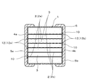
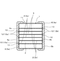
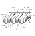
図1は、本願発明の一実施例にかかる積層セラミック電子部品(積層セラミックコンデンサ)の構成を示す図である。 FIG. 1 is a diagram showing a configuration of a multilayer ceramic electronic component (multilayer ceramic capacitor) according to an embodiment of the present invention.
この積層セラミックコンデンサにおいては、図1に示すように、セラミック積層体1中に、複数の内部電極(導体層)2がセラミック層3を介して積層されている。また、この複数の内部電極2(2a,2b)はセラミック積層体1の、互いに対向する一対の側面4a,4bに引き出されている。
In this multilayer ceramic capacitor, a plurality of internal electrodes (conductor layers) 2 are laminated via a
また、複数の内部電極2(2a,2b)は交互に、引出電極12(12a,12b)を介して、一対の側面4a,4bに配設された外部電極5a,5bのいずれか一方に電気的に接続されている。また、セラミック積層体1の、外部電極5a,5bが配設されていない領域は、絶縁性の樹脂からなる被覆層6により被覆されており、内部電極2(2a,2b)をセラミック積層体1の平面面積と同じ大きさにしているにもかかわらず、内部電極2(2a,2b)が外部と短絡したりすることがないように構成されている。
Also, the plurality of internal electrodes 2 (2a, 2b) are alternately connected to one of the
そして、この実施例の積層セラミックコンデンサにおいては、引出電極12(12a,12b)は、内部電極2a,2bの端部に撥水めっきを施して撥水めっき膜10を設けることにより形成されている。
In the multilayer ceramic capacitor of this embodiment, the lead electrodes 12 (12a, 12b) are formed by applying water-repellent plating to the ends of the
次に、この積層セラミックコンデンサの製造方法について説明する。
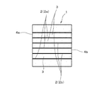
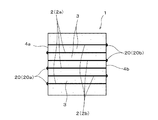
(1)一方主面に導体層が配設されたセラミックグリーンシートと、導体層(内部電極)が形成されていないセラミックグリーンシートを所定の順序で積層し、図2に示すように、複数の導体層2がセラミック層3を介して積層され、かつ、複数の導体層2が一対の側面4a,4bに引き出された構造を有する焼結済みのセラミック積層体1を用意する。
なお、このようなセラミック積層体は、通常の積層セラミック電子部品の製造工程で用いられる種々の方法、例えば、上述のようにセラミックグリーンシートを積層する工程を備えたいわゆるシート積層工法や、セラミックスラリーおよび電極ペーストを、図2に示すようなセラミック積層体1が形成されるように印刷してゆく、いわゆる逐次印刷工法などの方法により製造することが可能である。さらにその他の方法を適用することも可能である。
Next, a method for manufacturing this multilayer ceramic capacitor will be described.
(1) A ceramic green sheet in which a conductor layer is disposed on one main surface and a ceramic green sheet in which a conductor layer (internal electrode) is not formed are laminated in a predetermined order, and as shown in FIG. A sintered
In addition, such a ceramic laminated body can be obtained by various methods used in the production process of a normal multilayer ceramic electronic component, for example, a so-called sheet laminating method including a process of laminating ceramic green sheets as described above, or a ceramic slurry. In addition, the electrode paste can be manufactured by a method such as a so-called sequential printing method in which printing is performed so that the
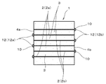
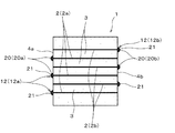
(2)それから、図3に示すように、セラミック積層体1の一対の側面4a,4bのうち、一方の側面4aに露出した導体層2(2a)に、1層おきに撥水性を有する引出電極12(12a)を形成するとともに、他方の側面4bに露出した導体層2のうち、一方の領域で一層おきに撥水性を有する引出電極12(12a)が形成された導体層2aとは異なる導体層2(2b)のそれぞれに撥水性を有する引出電極12(12b)を形成する。
この実施例では、所定の導体層(内部電極)に引出電極を形成するにあたっては、一層おきに導体層(引出電極を形成しない方の導体層)の端部をシールしておき、シールされていない方の導体層に撥水めっきを行うことにより、引出電極を形成した。
(2) Then, as shown in FIG. 3, the conductor layer 2 (2a) exposed on one
In this embodiment, when the extraction electrode is formed on the predetermined conductor layer (internal electrode), the end of the conductor layer (the conductor layer on which the extraction electrode is not formed) is sealed every other layer and sealed. A lead electrode was formed by performing water-repellent plating on the non-conductive layer.
撥水めっきを行うにあたっては、フッ素系高分子のエマルジョンとNiを含むめっき浴にセラミック積層体を積層して、Ni金属とともに、フッ素系高分子を共析させることにより撥水性を付与する方法を適用して、撥水性を有する引出電極(撥水めっき膜)を形成した。なお、引出電極を形成する方法については、下記の実施例2でも詳しく説明する。 In performing water-repellent plating, a method of providing water repellency by laminating a ceramic laminate in a plating bath containing a fluorine-based polymer emulsion and Ni and co-depositing the fluorine-based polymer together with Ni metal. By applying, an extraction electrode (water-repellent plating film) having water repellency was formed. The method for forming the extraction electrode will also be described in detail in Example 2 below.
フッ素系高分子としては、ポリテトラフルオロエチレン(PTFE)、ポリパーフルオロアルコキシブタジエン(PFA)、ポリフルオロビニリデンなどを単独で、あるいは、これらを組み合わせて用いることができる。撥水めっき膜の厚さは、1μm〜5μm程度であれば、本願発明において必要とされる撥水性を十分に確保することができる。 As the fluorine-based polymer, polytetrafluoroethylene (PTFE), polyperfluoroalkoxybutadiene (PFA), polyfluorovinylidene, or the like can be used alone or in combination. If the thickness of the water-repellent plating film is about 1 μm to 5 μm, the water repellency required in the present invention can be sufficiently secured.
なお、撥水めっき膜の厚さが1μm未満になると、撥水性が不十分になり、引出電極が被覆層により被覆されてしまう場合が生じるため好ましくない。また、撥水めっき膜が5μmを超えると、撥水性としては十分であるが、厚みが1μm以下の導体層(内部電極)に適用することが困難になるため好ましくない。 If the thickness of the water-repellent plating film is less than 1 μm, the water repellency becomes insufficient and the extraction electrode may be covered with the coating layer, which is not preferable. On the other hand, when the water-repellent plating film exceeds 5 μm, the water repellency is sufficient, but it is not preferable because it becomes difficult to apply to a conductor layer (internal electrode) having a thickness of 1 μm or less.
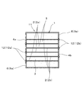
(3)次に、セラミック積層体1を、撥水めっき膜にはじかれる材料からなる被覆層により被覆して、図4に示すように、引出電極12(12a,12b)が露出し、他の領域が被覆層6により被覆された構造を有する被覆セラミック積層体11を形成する。
なお、セラミック積層体1を、撥水めっき膜にはじかれる材料からなる被覆層6により被覆する方法としては、例えば、絶縁樹脂原料の溶剤溶液などに浸漬した後、絶縁樹脂を硬化させる方法などを適用することができる。
また、後述のように、絶縁性のセラミック層を被覆層とする被覆セラミック積層体11を形成することも可能である。
(3) Next, the
Incidentally, the
Further, as will be described later, it is also possible to form a coated
(4)それから、引出電極12(12a,12b)が露出した被覆セラミック積層体11の両側面4a,4bに、引出電極12a,12bと導通するように外部電極形成用の導電ペーストを塗布し、焼き付けることにより、外部電極5a,5bを形成する。これにより、図1に示すような構造を有する積層セラミックコンデンサが得られる。
上記の方法により、例えば、内部電極2の厚みが2μm、引出電極12(12a,12b)を構成する撥水めっき膜10の膜厚が3μm、セラミック層3の厚みが5μmというような条件の積層セラミックコンデンサを効率よく製造することができる。
(4) Then, a conductive paste for forming an external electrode is applied to both
By the above method, for example, the lamination is performed such that the thickness of the
なお、この実施例1では、絶縁樹脂からなる被覆層6によりセラミック積層体1を被覆する場合を例にとって説明したが、耐熱性などの耐環境性を考慮すると、セラミックからなる被覆層によりセラミック積層体が被覆された構造とすることが望ましい場合がある。
その場合、例えば、未焼成の状態のセラミック積層体1に、撥水性を有する引出電極12(12a,12b)を形成した後、セラミックスラリーに浸漬して、図5に示すように、引出電極12(12a,12b)が露出し、他の領域がセラミック層からなる被覆層6(6a)により被覆された被覆セラミック積層体11を形成し、これを一体的に焼成した後、図6に示すように、外部電極5a,5bを形成することにより、セラミック積層体1がセラミック層からなる被覆層6(6a)により被覆された構造を有する積層セラミックコンデンサを得ることができる。
In the first embodiment, the case where the
In that case, for example, the extraction electrode 12 (12a, 12b) having water repellency is formed on the
なお、セラミック積層体1を被覆層6(6a)であるセラミック層で被覆するにあたっては、例えば、以下の方法が例示される。
例えば、セラミック積層体を構成するセラミックがチタン酸バリウム系セラミックである場合、同じくチタン酸バリウム系のセラミック原料を用い、これに有機ビヒクル、添加剤、および、溶剤を添加して混合し、粘度1〜10Pa・s(せん断速度100s−1での測定値)、セラミック固形分濃度10vol%のセラミックスラリーを準備する。
In coating the
For example, when the ceramic constituting the ceramic laminate is a barium titanate-based ceramic, a barium titanate-based ceramic raw material is also used, and an organic vehicle, an additive, and a solvent are added thereto and mixed to obtain a viscosity of 1 A ceramic slurry having 10 to 10 Pa · s (measured value at a shear rate of 100 s-1) and a ceramic solid content concentration of 10 vol% is prepared.
それから、所定の内部電極(導体層)に撥水めっきを施して引出電極(撥水めっき膜)を形成する、
また、例えば、内部電極の厚み2μm、撥水メッキ厚3μm、セラミック層の厚み5μmの、積層数10層のセラミック積層体を用意し、所定の内部電極(導体層)に撥水めっきを施して引出電極(撥水めっき膜)を形成する。
それから、このセラミック積層体を、上述のセラミックスラリーに浸漬した後、引き上げて、被覆層が固着しないようにフッ素樹脂コーティングしたポットに取り出し、30分間、回転させながら十分に乾燥させて、20μm厚の被覆層により被覆された、未焼成の被覆セラミック積層体11(図5参照)を得る。
Then, a predetermined internal electrode (conductor layer) is subjected to water repellent plating to form an extraction electrode (water repellent plated film).
Further, for example, a ceramic laminated body having a lamination number of 10 layers having a thickness of 2 μm for internal electrodes, a thickness of 3 μm for water repellent plating, and a thickness of 5 μm for ceramic layers is prepared, and water repellent plating is applied to predetermined internal electrodes (conductor layers). An extraction electrode (water-repellent plating film) is formed.
Then, after immersing this ceramic laminate in the above-mentioned ceramic slurry, it is pulled up and taken out into a pot coated with fluororesin so that the coating layer does not stick, and is dried sufficiently while rotating for 30 minutes, An unfired coated ceramic laminate 11 (see FIG. 5) covered with the coating layer is obtained.
そして、通常の方法で、1200℃の温度条件下にて焼成を行い、引出電極を除いて、全体が厚み15μmのセラミック層からなる被覆層により被覆された被覆セラミック積層体(焼結体)11を得る。 The coated ceramic laminate (sintered body) 11 is fired under a temperature condition of 1200 ° C. by a normal method, and the whole is covered with a coating layer made of a ceramic layer having a thickness of 15 μm except for the extraction electrode. Get.
その後、この被覆セラミック積層体11に外部電極5a,5bを形成することにより、図6に示すような構造を有する、セラミック積層体1がセラミック層からなる被覆層6(6a)により被覆された積層セラミックコンデンサが得られる。
After that, by forming
なお、セラミック積層体をセラミックスラリーにより被覆するにあたっては、例えば、セラミックスラリーを入れたバレルに、セラミック積層体を投入し、バレルを回転させる方法など種々の方法を採用することができるが、その方法に特別の制約はない。 In coating the ceramic laminate with the ceramic slurry, various methods such as, for example, a method of putting the ceramic laminate into a barrel containing the ceramic slurry and rotating the barrel can be adopted. There are no special restrictions.
<撥水性を有する引出電極の形成方法の変形例>
上記実施例1では、導体層の露出端部に撥水めっき膜を形成することにより引出電極を形成するようにしているが、導体層の露出端部に金めっきを施し、形成された金めっき膜の表面にフッ素変性チオールを塗布することによっても撥水性を有する引出電極を形成することができる。
<Modification of Method for Forming Extraction Electrode with Water Repellency>
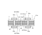
In Example 1 described above, the extraction electrode is formed by forming a water-repellent plating film on the exposed end portion of the conductor layer, but the exposed end portion of the conductor layer is subjected to gold plating, and the formed gold plating is formed. An extraction electrode having water repellency can also be formed by applying fluorine-modified thiol to the surface of the film.
すなわち、図7に示すように、セラミック積層体1の側面4a,4bのうちの一方の側面4aに露出した導体層2(2a)に、1層おきに金めっきを施して金めっき膜20(20a)を形成するとともに、他方の側面4bに露出した導体層2のうち、一方の側面4aで金めっき膜20(20a)が形成された導体層2aとは異なる導体層2(2b)のそれぞれに金めっきを施し、金めっき膜20(20b)を形成する。
That is, as shown in FIG. 7, the conductor layer 2 (2a) exposed on one
それから、図8に示すように、金めっき膜20(20a,20b)の表面にフッ素変性チオール21を塗布することにより、自己組織化膜を金めっき膜の表面に形成する。これにより、効率よく撥水性を有する引出電極12(12a,12b)を形成することができる。
Then, as shown in FIG. 8, a self-assembled film is formed on the surface of the gold plating film by applying fluorine-modified
その後は、上記実施例1の場合と同様の方法で、被覆層による被覆、外部電極の形成の工程を経て、図1に示す積層セラミックコンデンサに準じる構成を有する積層セラミックコンデンサを製造することができる。 Thereafter, a multilayer ceramic capacitor having a configuration similar to that of the multilayer ceramic capacitor shown in FIG. 1 can be manufactured through the steps of coating with a coating layer and forming an external electrode in the same manner as in Example 1. .
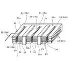
この実施例2では、マザー積層体を形成し、そこから複数の積層セラミックコンデンサを分割して多数個の積層セラミックコンデンサを同時に製造する、いわゆる多数個取りの方法により図1に示すような構造を有する積層セラミックコンデンサを製造する方法について説明する。 In Example 2, a mother multilayer body is formed, and a plurality of multilayer ceramic capacitors are divided therefrom to produce a large number of multilayer ceramic capacitors at the same time, so that a structure as shown in FIG. 1 is obtained. A method for manufacturing the laminated ceramic capacitor will be described.
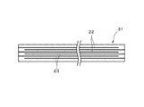
(1)まず、図9に示すように、複数の導体層22がセラミック層(セラミックグリーンシート)23を介して積層された構造を有する未焼成のマザーセラミック積層体31を形成する。
(1) First, as shown in FIG. 9, an unfired mother ceramic
(2)それから、図10に示すように、マザーセラミック積層体の所定の領域に、互いに平行な複数の溝30を形成することにより、以下の(a)〜(c)の要件を備えた溝付きマザーセラミック積層体31aを形成する。
(a)隣り合う一対の溝30に挟まれた領域の互いに対向する一対の側面24(24a,24b),が、図1に示す個々の積層セラミック電子部品を構成するセラミック積層体1の一対の側面4(4a,4b)となる、
(b)この一対の側面24(24a,24b)に複数の導体層22が露出している。
(c)複数の導体層22のそれぞれは、同一平面において、溝が形成されていない領域(基部)33(図10)で導通している。
(2) Then, as shown in FIG. 10, grooves having the following requirements (a) to (c) are formed by forming a plurality of
(a) A pair of side surfaces 24 (24a, 24b) facing each other in a region sandwiched between a pair of
(b) A plurality of conductor layers 22 are exposed on the pair of side surfaces 24 (24a, 24b).
(c) Each of the plurality of conductor layers 22 is electrically connected in a region (base) 33 (FIG. 10) where no groove is formed on the same plane.
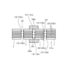
(3)そして、この溝付きマザーセラミック積層体31aの複数の溝30に、図11に示すように、一列おきにめっき液の浸入を阻止するためのマスク32aを施して、一列おきに溝30を密閉し、溝付きマザーセラミック積層体31aの一方側の端面34bに引き出された導体層22(22a)に電極36を接続して通電することにより撥水めっきを行い、図12に示すように、側面24a,24bに露出した導体層22(22a)に撥水めっき膜12(12a)を形成する。
(3) Then, as shown in FIG. 11, the plurality of
(4)それから、上記(3)の工程でマスク32aを施さなかった方の溝30に、図13に示すように、マスク32bを施して、(3)の工程で先に撥水めっき膜12(12a)を形成した溝30を密閉し、一層おきに、溝付きマザーセラミック積層体31aの一方側の端面34aに引き出された導体層22(22b)に電極36を接続して通電することにより撥水めっきを行い、図14に示すように、側面24a,24bに露出した導体層22(22b)に撥水めっき膜12(12b)を形成する。
(4) Then, as shown in FIG. 13, a
(5)次に、溝付きマザーセラミック積層体31aを切断して、個々のセラミック積層体1に分割する。これにより、図3に示すような構造を有する、引出電極12(12a,12b)を備えた個々のセラミック積層体1が得られる。
(5) Next, the mother
(6)その後は、実施例1の場合と同様に、セラミック積層体1を、引出電極12(12a,12b)にはじかれる材料からなる被覆層により被覆して、図4あるいは図5に示すように、引出電極12(12a,12b)が露出し、他の領域が被覆層6により被覆された構造を有する被覆セラミック積層体11を形成する。
(6) Thereafter, as in Example 1, the
(7)それから、引出電極12(12a,12b)が露出した被覆セラミック積層体11の両側面4a,4bに、引出電極12a,12bと導通するように外部電極形成用の導電ペーストを塗布し、焼き付けることにより、外部電極5a,5bを形成する。これにより、図1に示すような積層セラミックコンデンサに準じる構造を有する積層セラミックコンデンサが得られる。
(7) Then, a conductive paste for forming external electrodes is applied to both
また、この実施例2においても、導体層の露出端部に撥水めっき膜を形成することにより引出電極を形成するようにしているが、導体層の露出端部に金めっきを施し、形成された金めっき膜の表面にフッ素変性チオールを塗布することによっても撥水性を有する引出電極を形成することができる。 Also in Example 2, the extraction electrode is formed by forming a water-repellent plating film on the exposed end of the conductor layer. However, the exposed end of the conductor layer is formed by gold plating. An extraction electrode having water repellency can also be formed by applying fluorine-modified thiol to the surface of the gold plating film.
この実施例2の方法によれば、いわゆる多数個取りの方法により、製品寸法の平面面積と内部電極の面積が実質的に同一で、小型大容量の積層セラミックコンデンサを、内部電極のパターニングなどの工程を必要とすることなく、効率よく製造することができる。 According to the method of the second embodiment, a so-called multi-cavity method is used to manufacture a small-sized and large-capacity monolithic ceramic capacitor in which the planar area of the product dimensions and the area of the internal electrode are substantially the same, such as patterning of the internal electrode. It can manufacture efficiently, without requiring a process.
また、この実施例2の本願発明の方法によれば、特に位置決めなどの工程を必要とせず、多数のセラミック積層体を一括して処理することが可能であり、生産性を大幅に向上させることができるため、工業的な意義が大きい。 In addition, according to the method of the present invention of Example 2, it is possible to process a large number of ceramic laminates at the same time without requiring a step such as positioning, thereby greatly improving productivity. Therefore, it has great industrial significance.
なお、上記実施例では、積層セラミックコンデンサを例にとって説明したが、本願発明は、LC複合部品など、積層セラミックコンデンサ以外の積層セラミック電子部品にも適用することが可能である。 In the above embodiment, the multilayer ceramic capacitor has been described as an example. However, the present invention can also be applied to multilayer ceramic electronic components other than the multilayer ceramic capacitor, such as LC composite components.
本願発明は、その他の点においても上記実施例に限定されるものではなく、内部電極の積層数、引出電極の具体的な形成方法などに関し、発明の範囲内において、種々の応用、変形を加えることが可能である。 The invention of the present application is not limited to the above embodiment in other respects, and various applications and modifications are made within the scope of the invention with respect to the number of stacked internal electrodes and a specific method of forming the extraction electrode. It is possible.
上述のように、本願発明によれば、内部電極の面積を製品寸法の平面面積と実質的に同一とすることが可能で、内部電極のパターニング工程などを必要とすることなく、小型高特性の積層セラミック電子部品を効率よく製造することが可能になり、例えば、積層セラミックコンデンサの場合には、小型大容量化を実現することができる。
したがって、本願発明は、積層セラミックコンデンサや積層LC複合部品などの積層セラミック電子部品、その製造に関する技術分野に広く利用することが可能である。
As described above, according to the present invention, the area of the internal electrode can be made substantially the same as the planar area of the product dimension, and it is possible to reduce the size and high characteristics without requiring a patterning process of the internal electrode. A multilayer ceramic electronic component can be efficiently manufactured. For example, in the case of a multilayer ceramic capacitor, a small size and a large capacity can be realized.
Therefore, the present invention can be widely used in the technical fields related to multilayer ceramic electronic components such as multilayer ceramic capacitors and multilayer LC composite components and their manufacture.
1 セラミック積層体
2(2a,2b) 内部電極(導体層)
3 セラミック層
4a,4b セラミック積層体の側面
5a,5b 外部電極
6,6a 被覆層
10 撥水めっき膜
11 被覆セラミック積層体
12(12a,12b) 引出電極
20(20a,20b) 金めっき膜
21 フッ素変性チオール
22 導体層
23 セラミック層(セラミックグリーンシート)
24(24a,24b) 溝の側面
30 溝
31 未焼成のマザーセラミック積層体
31a 溝付きマザーセラミック積層体
32a,32b マスク
33 マザーセラミック積層体の溝が形成されていない領域(基部)
34a,34b 溝付きマザーセラミック積層体の端面
36 電極
1 Ceramic laminate 2 (2a, 2b) Internal electrode (conductor layer)
3
24 (24a, 24b) Side surface of
34a, 34b End face of grooved mother
Claims (5)
前記複数の導体層がセラミック層を介して積層され、かつ、前記一対の領域に引き出された構造を有するセラミック積層体を形成する工程と、
前記一対の領域のうちの一方の領域に露出した前記導体層に、1層おきに撥水性を付与しためっき膜である引出電極を形成する工程と、
前記一対の領域の他方の領域に露出した前記導体層のうち、前記一方の領域で一層おきに撥水性を付与しためっき膜である引出電極が形成された導体層とは異なる導体層のそれぞれに撥水性を付与しためっき膜である引出電極を形成する工程と、
前記引出電極に弾かれる材料からなる被覆層により前記セラミック積層体を被覆して、前記引出電極が前記被覆層から露出するとともに、他の所定の領域が前記被覆層により被覆された被覆セラミック積層体を形成する工程と、
前記被覆セラミック積層体の前記一対の領域に、前記引出電極と電気的に接続する外部電極を形成する工程と
を具備することを特徴とする積層セラミック電子部品の製造方法。 In the ceramic laminate, a plurality of conductor layers are laminated via a ceramic layer, and the plurality of conductor layers are alternately arranged in a pair of regions on the side surface of the ceramic laminate. On the other hand, a method for producing a multilayer ceramic electronic component having a structure electrically connected,
Forming a ceramic laminate having a structure in which the plurality of conductor layers are laminated via ceramic layers and drawn to the pair of regions;
Forming a lead electrode, which is a plating film provided with water repellency every other layer, on the conductor layer exposed in one of the pair of regions;
Of each of the conductor layers exposed in the other region of the pair of regions, each of the conductor layers different from the conductor layer formed with the extraction electrode, which is a plating film imparted with water repellency every other layer in the one region. Forming a lead electrode that is a plating film imparted with water repellency;
The ceramic laminate is coated with a coating layer made of a material repelled by the extraction electrode, the extraction electrode is exposed from the coating layer, and another predetermined region is coated with the coating layer. Forming a step;
Forming an external electrode electrically connected to the lead electrode in the pair of regions of the coated ceramic laminate. A method for producing a multilayer ceramic electronic component, comprising:
複数の導体層がセラミック層を介して積層されたマザーセラミック積層体を形成する工程と、
前記マザーセラミック積層体の所定の領域に、互いに平行な複数の溝を形成して、(a)隣り合う一対の溝に挟まれた領域の互いに対向する一対の側面が、個々の積層セラミック電子部品を構成するセラミック積層体の一対の側面となり、(b)前記側面に前記複数の導体層が露出し、(c)前記複数の導体層のそれぞれは、同一平面において、溝が形成されていない領域で導通した構造を有する溝付きマザーセラミック積層体を形成する工程と、
前記溝付きマザーセラミック積層体の前記一対の側面のうちの一方の側面に露出した前記導体層に、1層おきに撥水性を付与しためっき膜である引出電極を形成する工程と、
前記一対の側面の他方の側面に露出した前記導体層のうち、前記一方の側面で一層おきに撥水性を付与しためっき膜である引出電極が形成された導体層とは異なる導体層のそれぞれに撥水性を付与しためっき膜である引出電極を形成する工程と、
前記溝付きマザーセラミック積層体を所定の位置で切断して、個々のセラミック積層体に分割する工程と、
前記引出電極にはじかれる材料からなる被覆層により前記セラミック積層体を被覆して、前記引出電極が前記被覆層から露出するとともに、他の所定の領域が前記被覆層により被覆された被覆セラミック積層体を形成する工程と、
前記被覆セラミック積層体の、前記一対の側面に、前記引出電極と電気的に接続する外部電極を形成する工程と
を具備することを特徴とする積層セラミック電子部品の製造方法。 In the ceramic laminate, a plurality of conductor layers are laminated via a ceramic layer, and the plurality of conductor layers are alternately arranged in a pair of regions on the side surface of the ceramic laminate. On the other hand, a method for producing a multilayer ceramic electronic component having a structure electrically connected,
Forming a mother ceramic laminate in which a plurality of conductor layers are laminated via a ceramic layer;
A plurality of parallel grooves are formed in a predetermined region of the mother ceramic laminate, and (a) a pair of side surfaces opposed to each other between a pair of adjacent grooves is an individual multilayer ceramic electronic component (B) the plurality of conductor layers are exposed on the side surfaces, and (c) each of the plurality of conductor layers is a region in which no groove is formed on the same plane. Forming a grooved mother ceramic laminate having a conductive structure at
Forming a lead electrode, which is a plating film provided with water repellency every other layer, on the conductor layer exposed on one side surface of the pair of side surfaces of the grooved mother ceramic laminate;
Of the conductor layers exposed on the other side surface of the pair of side surfaces, each of the conductor layers different from the conductor layer on which the extraction electrode, which is a plating film imparted with water repellency on every other side surface, is formed. Forming a lead electrode that is a plating film imparted with water repellency;
Cutting the grooved mother ceramic laminate at a predetermined position and dividing it into individual ceramic laminates;
By covering the ceramic laminate by coating layers consisting of Haji Charles material to the extraction electrode, the extraction electrode with is exposed from the coating layer, coated ceramic laminate another predetermined area is covered by the covering layer Forming a step;
And a step of forming external electrodes electrically connected to the extraction electrodes on the pair of side surfaces of the coated ceramic laminate. A method for producing a multilayer ceramic electronic component, comprising:
セラミック積層体の、前記外部電極が配設されていない領域のうち、少なくとも前記導体層が露出した部分が被覆層により被覆されており、かつ、
前記内部電極と前記外部電極の接続部分には、撥水性を付与しためっき膜が存在していること
を特徴とする積層セラミック電子部品。 In the ceramic laminate, a plurality of conductor layers are laminated via a ceramic layer, and the plurality of conductor layers are alternately arranged in a pair of regions on the side surface of the ceramic laminate. On the other hand, a multilayer ceramic electronic component having an electrically connected structure,
Of the region where the external electrode is not disposed in the ceramic laminate, at least a portion where the conductor layer is exposed is covered with a coating layer, and
A multilayer ceramic electronic component, wherein a plating film imparted with water repellency is present at a connection portion between the internal electrode and the external electrode.
Priority Applications (1)
| Application Number | Priority Date | Filing Date | Title |
|---|---|---|---|
| JP2007075221A JP5259107B2 (en) | 2007-03-22 | 2007-03-22 | Multilayer ceramic electronic component and manufacturing method thereof |
Applications Claiming Priority (1)
| Application Number | Priority Date | Filing Date | Title |
|---|---|---|---|
| JP2007075221A JP5259107B2 (en) | 2007-03-22 | 2007-03-22 | Multilayer ceramic electronic component and manufacturing method thereof |
Publications (2)
| Publication Number | Publication Date |
|---|---|
| JP2008235698A JP2008235698A (en) | 2008-10-02 |
| JP5259107B2 true JP5259107B2 (en) | 2013-08-07 |
Family
ID=39908118
Family Applications (1)
| Application Number | Title | Priority Date | Filing Date |
|---|---|---|---|
| JP2007075221A Expired - Fee Related JP5259107B2 (en) | 2007-03-22 | 2007-03-22 | Multilayer ceramic electronic component and manufacturing method thereof |
Country Status (1)
| Country | Link |
|---|---|
| JP (1) | JP5259107B2 (en) |
Families Citing this family (4)
| Publication number | Priority date | Publication date | Assignee | Title |
|---|---|---|---|---|
| JP5768471B2 (en) * | 2010-05-19 | 2015-08-26 | 株式会社村田製作所 | Manufacturing method of ceramic electronic component |
| DE102012101351A1 (en) * | 2012-02-20 | 2013-08-22 | Epcos Ag | Multi-layer component and method for producing a multilayer component |
| JP6015781B2 (en) * | 2015-01-06 | 2016-10-26 | Tdk株式会社 | Piezoelectric element |
| KR102827670B1 (en) * | 2019-07-17 | 2025-07-02 | 삼성전기주식회사 | Multi-layered ceramic electroic components |
Family Cites Families (8)
| Publication number | Priority date | Publication date | Assignee | Title |
|---|---|---|---|---|
| JPS60196981A (en) * | 1984-03-21 | 1985-10-05 | Nec Corp | Manufacture of electrostrictive effect element |
| JPS61234580A (en) * | 1985-04-11 | 1986-10-18 | Jgc Corp | Laminated type electrostriction of piezoelectric element |
| JP3292009B2 (en) * | 1995-10-20 | 2002-06-17 | 株式会社村田製作所 | Method of manufacturing electrode-integrated green sheet and multilayer ceramic electronic component |
| JP3067698B2 (en) * | 1997-06-27 | 2000-07-17 | 松下電器産業株式会社 | Manufacturing method of multilayer ceramic electronic component |
| JP2002005174A (en) * | 2000-06-19 | 2002-01-09 | Nippon Densan Corp | Part of fluid dynamic pressure bearing, manufacturing method of the part, and motor and disc device using the part |
| JP4573956B2 (en) * | 2000-06-30 | 2010-11-04 | 京セラ株式会社 | Multilayer electronic component and manufacturing method thereof |
| JP2003109841A (en) * | 2001-10-01 | 2003-04-11 | Murata Mfg Co Ltd | Laminated electronic component and its manufacturing method |
| JP2006093532A (en) * | 2004-09-27 | 2006-04-06 | Matsushita Electric Ind Co Ltd | Electronic components |
-
2007
- 2007-03-22 JP JP2007075221A patent/JP5259107B2/en not_active Expired - Fee Related
Also Published As
| Publication number | Publication date |
|---|---|
| JP2008235698A (en) | 2008-10-02 |
Similar Documents
| Publication | Publication Date | Title |
|---|---|---|
| JP4992523B2 (en) | Multilayer ceramic electronic component and manufacturing method thereof | |
| KR102112107B1 (en) | Electronic component and method of producing electronic component | |
| JP6978163B2 (en) | Multilayer ceramic capacitors and their manufacturing methods | |
| US11145460B2 (en) | Multilayer ceramic electronic component | |
| JP5332475B2 (en) | Multilayer ceramic electronic component and manufacturing method thereof | |
| KR101681358B1 (en) | A multilayer ceramic capacitor and a method for manufactuaring the same | |
| US11049657B2 (en) | Multilayer ceramic electronic component | |
| US12131871B2 (en) | Electronic component and method for manufacturing electronic component | |
| KR20190044535A (en) | Method for manufacturing solid electrolytic capacitor and solid electrolytic capacitor | |
| US11232912B2 (en) | Solid electrolytic capacitor | |
| KR101397835B1 (en) | Multi-layered ceramic electronic parts and method of manufacturing the same | |
| KR20120104955A (en) | Manufacturing method for monolithic ceramic electronic component | |
| JP5259107B2 (en) | Multilayer ceramic electronic component and manufacturing method thereof | |
| JP4574267B2 (en) | Manufacturing method of multilayer electronic component and multilayer electronic component | |
| KR101659208B1 (en) | Multi-Layer Ceramic Electronic Component and Method of Fabricating the Same | |
| KR102727245B1 (en) | Method for manufacturing electronic component and apparatus for manufacturing electronic component | |
| JP2009239204A (en) | Manufacturing method for electronic component | |
| US20140259580A1 (en) | Method for fabricating solid electrolytic capacitors | |
| JP2000306763A (en) | Multilayer ceramic capacitor and manufacturing method thereof | |
| JP5879913B2 (en) | Manufacturing method of ceramic electronic component | |
| CN222168164U (en) | Multilayer Ceramic Capacitors | |
| KR20230122970A (en) | Multilayer ceramic capacitor and method for manufacturing multilayer ceramic capacitor | |
| KR100739491B1 (en) | High dielectric constant capacitor and its manufacturing method | |
| JP2009130151A (en) | Multilayer piezoelectric actuator | |
| KR101185885B1 (en) | Electro component embedded circuit substrate and the fabrication method thereof |
Legal Events
| Date | Code | Title | Description |
|---|---|---|---|
| A621 | Written request for application examination |
Free format text: JAPANESE INTERMEDIATE CODE: A621 Effective date: 20100217 |
|
| A977 | Report on retrieval |
Free format text: JAPANESE INTERMEDIATE CODE: A971007 Effective date: 20111128 |
|
| A131 | Notification of reasons for refusal |
Free format text: JAPANESE INTERMEDIATE CODE: A131 Effective date: 20111213 |
|
| A521 | Written amendment |
Free format text: JAPANESE INTERMEDIATE CODE: A523 Effective date: 20120209 |
|
| A02 | Decision of refusal |
Free format text: JAPANESE INTERMEDIATE CODE: A02 Effective date: 20120327 |
|
| A61 | First payment of annual fees (during grant procedure) |
Free format text: JAPANESE INTERMEDIATE CODE: A61 Effective date: 20130424 |
|
| FPAY | Renewal fee payment (event date is renewal date of database) |
Free format text: PAYMENT UNTIL: 20160502 Year of fee payment: 3 |
|
| R150 | Certificate of patent or registration of utility model |
Ref document number: 5259107 Country of ref document: JP Free format text: JAPANESE INTERMEDIATE CODE: R150 Free format text: JAPANESE INTERMEDIATE CODE: R150 |
|
| LAPS | Cancellation because of no payment of annual fees |