JP5250196B2 - Display device and electronic device - Google Patents
Display device and electronic device Download PDFInfo
- Publication number
- JP5250196B2 JP5250196B2 JP2006282392A JP2006282392A JP5250196B2 JP 5250196 B2 JP5250196 B2 JP 5250196B2 JP 2006282392 A JP2006282392 A JP 2006282392A JP 2006282392 A JP2006282392 A JP 2006282392A JP 5250196 B2 JP5250196 B2 JP 5250196B2
- Authority
- JP
- Japan
- Prior art keywords
- polarizing plate
- quarter
- reflective
- transparent electrode
- polarizer
- Prior art date
- Legal status (The legal status is an assumption and is not a legal conclusion. Google has not performed a legal analysis and makes no representation as to the accuracy of the status listed.)
- Expired - Fee Related
Links
- 239000010410 layer Substances 0.000 claims description 185
- 239000010408 film Substances 0.000 claims description 182
- 239000000758 substrate Substances 0.000 claims description 114
- 230000005540 biological transmission Effects 0.000 claims description 42
- 239000011229 interlayer Substances 0.000 claims description 40
- 238000010521 absorption reaction Methods 0.000 claims description 30
- 239000004065 semiconductor Substances 0.000 claims description 28
- 239000010409 thin film Substances 0.000 claims description 22
- 230000000694 effects Effects 0.000 claims description 3
- 239000002245 particle Substances 0.000 claims 4
- 230000010287 polarization Effects 0.000 description 40
- 239000000463 material Substances 0.000 description 37
- 238000000034 method Methods 0.000 description 25
- 229910052751 metal Inorganic materials 0.000 description 19
- 239000002184 metal Substances 0.000 description 19
- 238000002161 passivation Methods 0.000 description 17
- 229910052710 silicon Inorganic materials 0.000 description 17
- 239000010703 silicon Substances 0.000 description 17
- XUIMIQQOPSSXEZ-UHFFFAOYSA-N Silicon Chemical compound [Si] XUIMIQQOPSSXEZ-UHFFFAOYSA-N 0.000 description 16
- 238000002347 injection Methods 0.000 description 14
- 239000007924 injection Substances 0.000 description 14
- VYPSYNLAJGMNEJ-UHFFFAOYSA-N silicon dioxide Inorganic materials O=[Si]=O VYPSYNLAJGMNEJ-UHFFFAOYSA-N 0.000 description 13
- XLOMVQKBTHCTTD-UHFFFAOYSA-N Zinc monoxide Chemical compound [Zn]=O XLOMVQKBTHCTTD-UHFFFAOYSA-N 0.000 description 12
- 239000000956 alloy Substances 0.000 description 11
- 229910052782 aluminium Inorganic materials 0.000 description 11
- 229920000642 polymer Polymers 0.000 description 11
- 239000002356 single layer Substances 0.000 description 11
- 229910045601 alloy Inorganic materials 0.000 description 10
- 230000006870 function Effects 0.000 description 10
- 229910052814 silicon oxide Inorganic materials 0.000 description 10
- 238000004544 sputter deposition Methods 0.000 description 10
- -1 polyethylene terephthalate Polymers 0.000 description 9
- 229910052581 Si3N4 Inorganic materials 0.000 description 8
- 229910052783 alkali metal Inorganic materials 0.000 description 8
- 150000001340 alkali metals Chemical class 0.000 description 8
- 230000005525 hole transport Effects 0.000 description 8
- HQVNEWCFYHHQES-UHFFFAOYSA-N silicon nitride Chemical compound N12[Si]34N5[Si]62N3[Si]51N64 HQVNEWCFYHHQES-UHFFFAOYSA-N 0.000 description 8
- 229910052784 alkaline earth metal Inorganic materials 0.000 description 7
- 150000001342 alkaline earth metals Chemical class 0.000 description 7
- 239000011521 glass Substances 0.000 description 7
- AMGQUBHHOARCQH-UHFFFAOYSA-N indium;oxotin Chemical compound [In].[Sn]=O AMGQUBHHOARCQH-UHFFFAOYSA-N 0.000 description 7
- 238000004519 manufacturing process Methods 0.000 description 7
- 150000002894 organic compounds Chemical class 0.000 description 7
- 238000005268 plasma chemical vapour deposition Methods 0.000 description 7
- 239000010936 titanium Substances 0.000 description 7
- UHOVQNZJYSORNB-UHFFFAOYSA-N Benzene Chemical group C1=CC=CC=C1 UHOVQNZJYSORNB-UHFFFAOYSA-N 0.000 description 6
- KPUWHANPEXNPJT-UHFFFAOYSA-N disiloxane Chemical class [SiH3]O[SiH3] KPUWHANPEXNPJT-UHFFFAOYSA-N 0.000 description 6
- 229910052739 hydrogen Inorganic materials 0.000 description 6
- 229910044991 metal oxide Inorganic materials 0.000 description 6
- 150000004706 metal oxides Chemical class 0.000 description 6
- 239000000565 sealant Substances 0.000 description 6
- 238000007789 sealing Methods 0.000 description 6
- 239000000126 substance Substances 0.000 description 6
- 239000002585 base Substances 0.000 description 5
- 150000001875 compounds Chemical class 0.000 description 5
- 238000002425 crystallisation Methods 0.000 description 5
- 239000001257 hydrogen Substances 0.000 description 5
- 238000005984 hydrogenation reaction Methods 0.000 description 5
- 239000012535 impurity Substances 0.000 description 5
- 229910003437 indium oxide Inorganic materials 0.000 description 5
- PJXISJQVUVHSOJ-UHFFFAOYSA-N indium(iii) oxide Chemical compound [O-2].[O-2].[O-2].[In+3].[In+3] PJXISJQVUVHSOJ-UHFFFAOYSA-N 0.000 description 5
- 229910000476 molybdenum oxide Inorganic materials 0.000 description 5
- 229910052757 nitrogen Inorganic materials 0.000 description 5
- 229910001925 ruthenium oxide Inorganic materials 0.000 description 5
- WOCIAKWEIIZHES-UHFFFAOYSA-N ruthenium(iv) oxide Chemical compound O=[Ru]=O WOCIAKWEIIZHES-UHFFFAOYSA-N 0.000 description 5
- MZLGASXMSKOWSE-UHFFFAOYSA-N tantalum nitride Chemical compound [Ta]#N MZLGASXMSKOWSE-UHFFFAOYSA-N 0.000 description 5
- 229910052719 titanium Inorganic materials 0.000 description 5
- 229910001935 vanadium oxide Inorganic materials 0.000 description 5
- UFHFLCQGNIYNRP-UHFFFAOYSA-N Hydrogen Chemical compound [H][H] UFHFLCQGNIYNRP-UHFFFAOYSA-N 0.000 description 4
- XAGFODPZIPBFFR-UHFFFAOYSA-N aluminium Chemical compound [Al] XAGFODPZIPBFFR-UHFFFAOYSA-N 0.000 description 4
- 230000015572 biosynthetic process Effects 0.000 description 4
- 239000010949 copper Substances 0.000 description 4
- 238000010586 diagram Methods 0.000 description 4
- 238000010438 heat treatment Methods 0.000 description 4
- 229910052744 lithium Inorganic materials 0.000 description 4
- 229920003023 plastic Polymers 0.000 description 4
- 239000004033 plastic Substances 0.000 description 4
- 230000008569 process Effects 0.000 description 4
- 229920005989 resin Polymers 0.000 description 4
- 239000011347 resin Substances 0.000 description 4
- 229910052721 tungsten Inorganic materials 0.000 description 4
- BCMCBBGGLRIHSE-UHFFFAOYSA-N 1,3-benzoxazole Chemical class C1=CC=C2OC=NC2=C1 BCMCBBGGLRIHSE-UHFFFAOYSA-N 0.000 description 3
- IJGRMHOSHXDMSA-UHFFFAOYSA-N Atomic nitrogen Chemical compound N#N IJGRMHOSHXDMSA-UHFFFAOYSA-N 0.000 description 3
- GYHNNYVSQQEPJS-UHFFFAOYSA-N Gallium Chemical compound [Ga] GYHNNYVSQQEPJS-UHFFFAOYSA-N 0.000 description 3
- XHCLAFWTIXFWPH-UHFFFAOYSA-N [O-2].[O-2].[O-2].[O-2].[O-2].[V+5].[V+5] Chemical compound [O-2].[O-2].[O-2].[O-2].[O-2].[V+5].[V+5] XHCLAFWTIXFWPH-UHFFFAOYSA-N 0.000 description 3
- NIXOWILDQLNWCW-UHFFFAOYSA-N acrylic acid group Chemical group C(C=C)(=O)O NIXOWILDQLNWCW-UHFFFAOYSA-N 0.000 description 3
- 230000000903 blocking effect Effects 0.000 description 3
- 239000000919 ceramic Substances 0.000 description 3
- 229910052802 copper Inorganic materials 0.000 description 3
- 238000009792 diffusion process Methods 0.000 description 3
- 229910052733 gallium Inorganic materials 0.000 description 3
- 238000010030 laminating Methods 0.000 description 3
- 229910052750 molybdenum Inorganic materials 0.000 description 3
- PQQKPALAQIIWST-UHFFFAOYSA-N oxomolybdenum Chemical compound [Mo]=O PQQKPALAQIIWST-UHFFFAOYSA-N 0.000 description 3
- 229920003227 poly(N-vinyl carbazole) Polymers 0.000 description 3
- 229910052709 silver Inorganic materials 0.000 description 3
- 125000001424 substituent group Chemical group 0.000 description 3
- 229910052715 tantalum Inorganic materials 0.000 description 3
- 239000011701 zinc Substances 0.000 description 3
- YVTHLONGBIQYBO-UHFFFAOYSA-N zinc indium(3+) oxygen(2-) Chemical compound [O--].[Zn++].[In+3] YVTHLONGBIQYBO-UHFFFAOYSA-N 0.000 description 3
- 239000011787 zinc oxide Substances 0.000 description 3
- STTGYIUESPWXOW-UHFFFAOYSA-N 2,9-dimethyl-4,7-diphenyl-1,10-phenanthroline Chemical compound C=12C=CC3=C(C=4C=CC=CC=4)C=C(C)N=C3C2=NC(C)=CC=1C1=CC=CC=C1 STTGYIUESPWXOW-UHFFFAOYSA-N 0.000 description 2
- UOCMXZLNHQBBOS-UHFFFAOYSA-N 2-(1,3-benzoxazol-2-yl)phenol zinc Chemical compound [Zn].Oc1ccccc1-c1nc2ccccc2o1.Oc1ccccc1-c1nc2ccccc2o1 UOCMXZLNHQBBOS-UHFFFAOYSA-N 0.000 description 2
- ZVFQEOPUXVPSLB-UHFFFAOYSA-N 3-(4-tert-butylphenyl)-4-phenyl-5-(4-phenylphenyl)-1,2,4-triazole Chemical compound C1=CC(C(C)(C)C)=CC=C1C(N1C=2C=CC=CC=2)=NN=C1C1=CC=C(C=2C=CC=CC=2)C=C1 ZVFQEOPUXVPSLB-UHFFFAOYSA-N 0.000 description 2
- DHDHJYNTEFLIHY-UHFFFAOYSA-N 4,7-diphenyl-1,10-phenanthroline Chemical compound C1=CC=CC=C1C1=CC=NC2=C1C=CC1=C(C=3C=CC=CC=3)C=CN=C21 DHDHJYNTEFLIHY-UHFFFAOYSA-N 0.000 description 2
- 229910017073 AlLi Inorganic materials 0.000 description 2
- 229910004261 CaF 2 Inorganic materials 0.000 description 2
- 241000284156 Clerodendrum quadriloculare Species 0.000 description 2
- 229920001609 Poly(3,4-ethylenedioxythiophene) Polymers 0.000 description 2
- 239000004642 Polyimide Substances 0.000 description 2
- BQCADISMDOOEFD-UHFFFAOYSA-N Silver Chemical compound [Ag] BQCADISMDOOEFD-UHFFFAOYSA-N 0.000 description 2
- 229910006404 SnO 2 Inorganic materials 0.000 description 2
- 239000007983 Tris buffer Substances 0.000 description 2
- 230000004888 barrier function Effects 0.000 description 2
- WPYMKLBDIGXBTP-UHFFFAOYSA-N benzoic acid Chemical compound OC(=O)C1=CC=CC=C1 WPYMKLBDIGXBTP-UHFFFAOYSA-N 0.000 description 2
- UFVXQDWNSAGPHN-UHFFFAOYSA-K bis[(2-methylquinolin-8-yl)oxy]-(4-phenylphenoxy)alumane Chemical compound [Al+3].C1=CC=C([O-])C2=NC(C)=CC=C21.C1=CC=C([O-])C2=NC(C)=CC=C21.C1=CC([O-])=CC=C1C1=CC=CC=C1 UFVXQDWNSAGPHN-UHFFFAOYSA-K 0.000 description 2
- 238000005229 chemical vapour deposition Methods 0.000 description 2
- 230000003098 cholesteric effect Effects 0.000 description 2
- 150000004696 coordination complex Chemical class 0.000 description 2
- 230000008025 crystallization Effects 0.000 description 2
- 239000007772 electrode material Substances 0.000 description 2
- 238000000605 extraction Methods 0.000 description 2
- 230000002349 favourable effect Effects 0.000 description 2
- 125000001153 fluoro group Chemical group F* 0.000 description 2
- 239000007789 gas Substances 0.000 description 2
- 229910052737 gold Inorganic materials 0.000 description 2
- 229910010272 inorganic material Inorganic materials 0.000 description 2
- 238000009413 insulation Methods 0.000 description 2
- 238000004518 low pressure chemical vapour deposition Methods 0.000 description 2
- 229910052749 magnesium Inorganic materials 0.000 description 2
- 229910052748 manganese Inorganic materials 0.000 description 2
- IBHBKWKFFTZAHE-UHFFFAOYSA-N n-[4-[4-(n-naphthalen-1-ylanilino)phenyl]phenyl]-n-phenylnaphthalen-1-amine Chemical group C1=CC=CC=C1N(C=1C2=CC=CC=C2C=CC=1)C1=CC=C(C=2C=CC(=CC=2)N(C=2C=CC=CC=2)C=2C3=CC=CC=C3C=CC=2)C=C1 IBHBKWKFFTZAHE-UHFFFAOYSA-N 0.000 description 2
- 229910052759 nickel Inorganic materials 0.000 description 2
- 150000004767 nitrides Chemical class 0.000 description 2
- 239000012299 nitrogen atmosphere Substances 0.000 description 2
- QGLKJKCYBOYXKC-UHFFFAOYSA-N nonaoxidotritungsten Chemical compound O=[W]1(=O)O[W](=O)(=O)O[W](=O)(=O)O1 QGLKJKCYBOYXKC-UHFFFAOYSA-N 0.000 description 2
- 125000000962 organic group Chemical group 0.000 description 2
- 239000011368 organic material Substances 0.000 description 2
- AHLBNYSZXLDEJQ-FWEHEUNISA-N orlistat Chemical compound CCCCCCCCCCC[C@H](OC(=O)[C@H](CC(C)C)NC=O)C[C@@H]1OC(=O)[C@H]1CCCCCC AHLBNYSZXLDEJQ-FWEHEUNISA-N 0.000 description 2
- JMANVNJQNLATNU-UHFFFAOYSA-N oxalonitrile Chemical compound N#CC#N JMANVNJQNLATNU-UHFFFAOYSA-N 0.000 description 2
- 229910052760 oxygen Inorganic materials 0.000 description 2
- IEQIEDJGQAUEQZ-UHFFFAOYSA-N phthalocyanine Chemical compound N1C(N=C2C3=CC=CC=C3C(N=C3C4=CC=CC=C4C(=N4)N3)=N2)=C(C=CC=C2)C2=C1N=C1C2=CC=CC=C2C4=N1 IEQIEDJGQAUEQZ-UHFFFAOYSA-N 0.000 description 2
- 229910052697 platinum Inorganic materials 0.000 description 2
- BASFCYQUMIYNBI-UHFFFAOYSA-N platinum Substances [Pt] BASFCYQUMIYNBI-UHFFFAOYSA-N 0.000 description 2
- 229910021420 polycrystalline silicon Inorganic materials 0.000 description 2
- 229920001721 polyimide Polymers 0.000 description 2
- 229920000123 polythiophene Polymers 0.000 description 2
- 230000001681 protective effect Effects 0.000 description 2
- 239000011241 protective layer Substances 0.000 description 2
- 239000010453 quartz Substances 0.000 description 2
- 238000001552 radio frequency sputter deposition Methods 0.000 description 2
- 230000009467 reduction Effects 0.000 description 2
- 238000002310 reflectometry Methods 0.000 description 2
- 239000004332 silver Substances 0.000 description 2
- XOLBLPGZBRYERU-UHFFFAOYSA-N tin dioxide Chemical compound O=[Sn]=O XOLBLPGZBRYERU-UHFFFAOYSA-N 0.000 description 2
- 229910001887 tin oxide Inorganic materials 0.000 description 2
- 229910001930 tungsten oxide Inorganic materials 0.000 description 2
- 238000007740 vapor deposition Methods 0.000 description 2
- POILWHVDKZOXJZ-ARJAWSKDSA-M (z)-4-oxopent-2-en-2-olate Chemical compound C\C([O-])=C\C(C)=O POILWHVDKZOXJZ-ARJAWSKDSA-M 0.000 description 1
- IYZMXHQDXZKNCY-UHFFFAOYSA-N 1-n,1-n-diphenyl-4-n,4-n-bis[4-(n-phenylanilino)phenyl]benzene-1,4-diamine Chemical compound C1=CC=CC=C1N(C=1C=CC(=CC=1)N(C=1C=CC(=CC=1)N(C=1C=CC=CC=1)C=1C=CC=CC=1)C=1C=CC(=CC=1)N(C=1C=CC=CC=1)C=1C=CC=CC=1)C1=CC=CC=C1 IYZMXHQDXZKNCY-UHFFFAOYSA-N 0.000 description 1
- VFMUXPQZKOKPOF-UHFFFAOYSA-N 2,3,7,8,12,13,17,18-octaethyl-21,23-dihydroporphyrin platinum Chemical compound [Pt].CCc1c(CC)c2cc3[nH]c(cc4nc(cc5[nH]c(cc1n2)c(CC)c5CC)c(CC)c4CC)c(CC)c3CC VFMUXPQZKOKPOF-UHFFFAOYSA-N 0.000 description 1
- SNTWKPAKVQFCCF-UHFFFAOYSA-N 2,3-dihydro-1h-triazole Chemical compound N1NC=CN1 SNTWKPAKVQFCCF-UHFFFAOYSA-N 0.000 description 1
- FQJQNLKWTRGIEB-UHFFFAOYSA-N 2-(4-tert-butylphenyl)-5-[3-[5-(4-tert-butylphenyl)-1,3,4-oxadiazol-2-yl]phenyl]-1,3,4-oxadiazole Chemical compound C1=CC(C(C)(C)C)=CC=C1C1=NN=C(C=2C=C(C=CC=2)C=2OC(=NN=2)C=2C=CC(=CC=2)C(C)(C)C)O1 FQJQNLKWTRGIEB-UHFFFAOYSA-N 0.000 description 1
- GEQBRULPNIVQPP-UHFFFAOYSA-N 2-[3,5-bis(1-phenylbenzimidazol-2-yl)phenyl]-1-phenylbenzimidazole Chemical compound C1=CC=CC=C1N1C2=CC=CC=C2N=C1C1=CC(C=2N(C3=CC=CC=C3N=2)C=2C=CC=CC=2)=CC(C=2N(C3=CC=CC=C3N=2)C=2C=CC=CC=2)=C1 GEQBRULPNIVQPP-UHFFFAOYSA-N 0.000 description 1
- OGGKVJMNFFSDEV-UHFFFAOYSA-N 3-methyl-n-[4-[4-(n-(3-methylphenyl)anilino)phenyl]phenyl]-n-phenylaniline Chemical group CC1=CC=CC(N(C=2C=CC=CC=2)C=2C=CC(=CC=2)C=2C=CC(=CC=2)N(C=2C=CC=CC=2)C=2C=C(C)C=CC=2)=C1 OGGKVJMNFFSDEV-UHFFFAOYSA-N 0.000 description 1
- AWXGSYPUMWKTBR-UHFFFAOYSA-N 4-carbazol-9-yl-n,n-bis(4-carbazol-9-ylphenyl)aniline Chemical compound C12=CC=CC=C2C2=CC=CC=C2N1C1=CC=C(N(C=2C=CC(=CC=2)N2C3=CC=CC=C3C3=CC=CC=C32)C=2C=CC(=CC=2)N2C3=CC=CC=C3C3=CC=CC=C32)C=C1 AWXGSYPUMWKTBR-UHFFFAOYSA-N 0.000 description 1
- 125000004860 4-ethylphenyl group Chemical group [H]C1=C([H])C(=C([H])C([H])=C1*)C([H])([H])C([H])([H])[H] 0.000 description 1
- DIVZFUBWFAOMCW-UHFFFAOYSA-N 4-n-(3-methylphenyl)-1-n,1-n-bis[4-(n-(3-methylphenyl)anilino)phenyl]-4-n-phenylbenzene-1,4-diamine Chemical compound CC1=CC=CC(N(C=2C=CC=CC=2)C=2C=CC(=CC=2)N(C=2C=CC(=CC=2)N(C=2C=CC=CC=2)C=2C=C(C)C=CC=2)C=2C=CC(=CC=2)N(C=2C=CC=CC=2)C=2C=C(C)C=CC=2)=C1 DIVZFUBWFAOMCW-UHFFFAOYSA-N 0.000 description 1
- 229910000838 Al alloy Inorganic materials 0.000 description 1
- 239000005711 Benzoic acid Substances 0.000 description 1
- NLZUEZXRPGMBCV-UHFFFAOYSA-N Butylhydroxytoluene Chemical compound CC1=CC(C(C)(C)C)=C(O)C(C(C)(C)C)=C1 NLZUEZXRPGMBCV-UHFFFAOYSA-N 0.000 description 1
- OKTJSMMVPCPJKN-UHFFFAOYSA-N Carbon Chemical compound [C] OKTJSMMVPCPJKN-UHFFFAOYSA-N 0.000 description 1
- 229910052691 Erbium Inorganic materials 0.000 description 1
- 101000837344 Homo sapiens T-cell leukemia translocation-altered gene protein Proteins 0.000 description 1
- 229910018068 Li 2 O Inorganic materials 0.000 description 1
- WHXSMMKQMYFTQS-UHFFFAOYSA-N Lithium Chemical compound [Li] WHXSMMKQMYFTQS-UHFFFAOYSA-N 0.000 description 1
- 229910052779 Neodymium Inorganic materials 0.000 description 1
- 229910018106 Ni—C Inorganic materials 0.000 description 1
- OAICVXFJPJFONN-UHFFFAOYSA-N Phosphorus Chemical compound [P] OAICVXFJPJFONN-UHFFFAOYSA-N 0.000 description 1
- 239000004952 Polyamide Substances 0.000 description 1
- 239000004695 Polyether sulfone Substances 0.000 description 1
- 239000004743 Polypropylene Substances 0.000 description 1
- NRCMAYZCPIVABH-UHFFFAOYSA-N Quinacridone Chemical class N1C2=CC=CC=C2C(=O)C2=C1C=C1C(=O)C3=CC=CC=C3NC1=C2 NRCMAYZCPIVABH-UHFFFAOYSA-N 0.000 description 1
- 229910007991 Si-N Inorganic materials 0.000 description 1
- 229910006294 Si—N Inorganic materials 0.000 description 1
- 102100028692 T-cell leukemia translocation-altered gene protein Human genes 0.000 description 1
- GWEVSGVZZGPLCZ-UHFFFAOYSA-N Titan oxide Chemical compound O=[Ti]=O GWEVSGVZZGPLCZ-UHFFFAOYSA-N 0.000 description 1
- BZHJMEDXRYGGRV-UHFFFAOYSA-N Vinyl chloride Chemical compound ClC=C BZHJMEDXRYGGRV-UHFFFAOYSA-N 0.000 description 1
- 229910052769 Ytterbium Inorganic materials 0.000 description 1
- HCHKCACWOHOZIP-UHFFFAOYSA-N Zinc Chemical compound [Zn] HCHKCACWOHOZIP-UHFFFAOYSA-N 0.000 description 1
- DDRUQPGRDYOZHB-UHFFFAOYSA-N [Eu].c1ccc2c(c1)ccc1ccccc21 Chemical compound [Eu].c1ccc2c(c1)ccc1ccccc21 DDRUQPGRDYOZHB-UHFFFAOYSA-N 0.000 description 1
- CUJRVFIICFDLGR-UHFFFAOYSA-N acetylacetonate Chemical compound CC(=O)[CH-]C(C)=O CUJRVFIICFDLGR-UHFFFAOYSA-N 0.000 description 1
- 230000009471 action Effects 0.000 description 1
- 238000001994 activation Methods 0.000 description 1
- 230000002411 adverse Effects 0.000 description 1
- 229910001508 alkali metal halide Inorganic materials 0.000 description 1
- 150000008045 alkali metal halides Chemical class 0.000 description 1
- 229910000272 alkali metal oxide Inorganic materials 0.000 description 1
- 125000000217 alkyl group Chemical group 0.000 description 1
- 125000005376 alkyl siloxane group Chemical group 0.000 description 1
- 239000005407 aluminoborosilicate glass Substances 0.000 description 1
- 150000001412 amines Chemical class 0.000 description 1
- 229910021417 amorphous silicon Inorganic materials 0.000 description 1
- 238000000137 annealing Methods 0.000 description 1
- 150000004982 aromatic amines Chemical class 0.000 description 1
- 150000001491 aromatic compounds Chemical class 0.000 description 1
- 150000004945 aromatic hydrocarbons Chemical class 0.000 description 1
- 239000012298 atmosphere Substances 0.000 description 1
- QVGXLLKOCUKJST-UHFFFAOYSA-N atomic oxygen Chemical compound [O] QVGXLLKOCUKJST-UHFFFAOYSA-N 0.000 description 1
- 230000002238 attenuated effect Effects 0.000 description 1
- 229910052788 barium Inorganic materials 0.000 description 1
- DSAJWYNOEDNPEQ-UHFFFAOYSA-N barium atom Chemical compound [Ba] DSAJWYNOEDNPEQ-UHFFFAOYSA-N 0.000 description 1
- WZJYKHNJTSNBHV-UHFFFAOYSA-N benzo[h]quinoline Chemical group C1=CN=C2C3=CC=CC=C3C=CC2=C1 WZJYKHNJTSNBHV-UHFFFAOYSA-N 0.000 description 1
- 235000010233 benzoic acid Nutrition 0.000 description 1
- 229910052790 beryllium Inorganic materials 0.000 description 1
- ATBAMAFKBVZNFJ-UHFFFAOYSA-N beryllium atom Chemical compound [Be] ATBAMAFKBVZNFJ-UHFFFAOYSA-N 0.000 description 1
- 239000005388 borosilicate glass Substances 0.000 description 1
- XZCJVWCMJYNSQO-UHFFFAOYSA-N butyl pbd Chemical compound C1=CC(C(C)(C)C)=CC=C1C1=NN=C(C=2C=CC(=CC=2)C=2C=CC=CC=2)O1 XZCJVWCMJYNSQO-UHFFFAOYSA-N 0.000 description 1
- 229910052792 caesium Inorganic materials 0.000 description 1
- 229910052791 calcium Inorganic materials 0.000 description 1
- 239000003990 capacitor Substances 0.000 description 1
- 229910052799 carbon Inorganic materials 0.000 description 1
- 230000001413 cellular effect Effects 0.000 description 1
- 238000006243 chemical reaction Methods 0.000 description 1
- 229910052804 chromium Inorganic materials 0.000 description 1
- 239000003086 colorant Substances 0.000 description 1
- 239000004020 conductor Substances 0.000 description 1
- PMHQVHHXPFUNSP-UHFFFAOYSA-M copper(1+);methylsulfanylmethane;bromide Chemical compound Br[Cu].CSC PMHQVHHXPFUNSP-UHFFFAOYSA-M 0.000 description 1
- 150000001893 coumarin derivatives Chemical class 0.000 description 1
- 239000013078 crystal Substances 0.000 description 1
- CFBGXYDUODCMNS-UHFFFAOYSA-N cyclobutene Chemical compound C1CC=C1 CFBGXYDUODCMNS-UHFFFAOYSA-N 0.000 description 1
- 230000018044 dehydration Effects 0.000 description 1
- 238000006297 dehydration reaction Methods 0.000 description 1
- 230000006866 deterioration Effects 0.000 description 1
- 238000005401 electroluminescence Methods 0.000 description 1
- 238000005530 etching Methods 0.000 description 1
- 230000001747 exhibiting effect Effects 0.000 description 1
- 239000000284 extract Substances 0.000 description 1
- 239000000945 filler Substances 0.000 description 1
- 239000007850 fluorescent dye Substances 0.000 description 1
- 150000004820 halides Chemical class 0.000 description 1
- RBTKNAXYKSUFRK-UHFFFAOYSA-N heliogen blue Chemical compound [Cu].[N-]1C2=C(C=CC=C3)C3=C1N=C([N-]1)C3=CC=CC=C3C1=NC([N-]1)=C(C=CC=C3)C3=C1N=C([N-]1)C3=CC=CC=C3C1=N2 RBTKNAXYKSUFRK-UHFFFAOYSA-N 0.000 description 1
- 150000002431 hydrogen Chemical class 0.000 description 1
- 150000002460 imidazoles Chemical class 0.000 description 1
- 239000011261 inert gas Substances 0.000 description 1
- 150000002484 inorganic compounds Chemical class 0.000 description 1
- 239000011147 inorganic material Substances 0.000 description 1
- 239000012212 insulator Substances 0.000 description 1
- 229940079865 intestinal antiinfectives imidazole derivative Drugs 0.000 description 1
- UEEXRMUCXBPYOV-UHFFFAOYSA-N iridium;2-phenylpyridine Chemical compound [Ir].C1=CC=CC=C1C1=CC=CC=N1.C1=CC=CC=C1C1=CC=CC=N1.C1=CC=CC=C1C1=CC=CC=N1 UEEXRMUCXBPYOV-UHFFFAOYSA-N 0.000 description 1
- 238000005224 laser annealing Methods 0.000 description 1
- 238000005499 laser crystallization Methods 0.000 description 1
- 239000002346 layers by function Substances 0.000 description 1
- 239000003446 ligand Substances 0.000 description 1
- 239000004973 liquid crystal related substance Substances 0.000 description 1
- 238000002156 mixing Methods 0.000 description 1
- 239000000203 mixture Substances 0.000 description 1
- 230000003287 optical effect Effects 0.000 description 1
- 150000004866 oxadiazoles Chemical class 0.000 description 1
- 230000003647 oxidation Effects 0.000 description 1
- 238000007254 oxidation reaction Methods 0.000 description 1
- TWNQGVIAIRXVLR-UHFFFAOYSA-N oxo(oxoalumanyloxy)alumane Chemical compound O=[Al]O[Al]=O TWNQGVIAIRXVLR-UHFFFAOYSA-N 0.000 description 1
- 239000001301 oxygen Substances 0.000 description 1
- 238000005192 partition Methods 0.000 description 1
- 229910052698 phosphorus Inorganic materials 0.000 description 1
- 239000011574 phosphorus Substances 0.000 description 1
- 238000005498 polishing Methods 0.000 description 1
- 229920000172 poly(styrenesulfonic acid) Polymers 0.000 description 1
- 229920002647 polyamide Polymers 0.000 description 1
- 229920000767 polyaniline Polymers 0.000 description 1
- 229920001230 polyarylate Polymers 0.000 description 1
- 239000004417 polycarbonate Substances 0.000 description 1
- 229920000515 polycarbonate Polymers 0.000 description 1
- 229920000728 polyester Polymers 0.000 description 1
- 229920006393 polyether sulfone Polymers 0.000 description 1
- 229920000139 polyethylene terephthalate Polymers 0.000 description 1
- 239000005020 polyethylene terephthalate Substances 0.000 description 1
- 239000002861 polymer material Substances 0.000 description 1
- 238000006116 polymerization reaction Methods 0.000 description 1
- 229920001155 polypropylene Polymers 0.000 description 1
- 229920001709 polysilazane Polymers 0.000 description 1
- 229920005591 polysilicon Polymers 0.000 description 1
- 229940005642 polystyrene sulfonic acid Drugs 0.000 description 1
- 229920002620 polyvinyl fluoride Polymers 0.000 description 1
- 230000002265 prevention Effects 0.000 description 1
- 125000002943 quinolinyl group Chemical group N1=C(C=CC2=CC=CC=C12)* 0.000 description 1
- 229910052761 rare earth metal Inorganic materials 0.000 description 1
- 150000002910 rare earth metals Chemical class 0.000 description 1
- YYMBJDOZVAITBP-UHFFFAOYSA-N rubrene Chemical compound C1=CC=CC=C1C(C1=C(C=2C=CC=CC=2)C2=CC=CC=C2C(C=2C=CC=CC=2)=C11)=C(C=CC=C2)C2=C1C1=CC=CC=C1 YYMBJDOZVAITBP-UHFFFAOYSA-N 0.000 description 1
- 150000003376 silicon Chemical class 0.000 description 1
- 239000010935 stainless steel Substances 0.000 description 1
- 229910001220 stainless steel Inorganic materials 0.000 description 1
- PJANXHGTPQOBST-UHFFFAOYSA-N stilbene Chemical class C=1C=CC=CC=1C=CC1=CC=CC=C1 PJANXHGTPQOBST-UHFFFAOYSA-N 0.000 description 1
- 229910052712 strontium Inorganic materials 0.000 description 1
- 229920003002 synthetic resin Polymers 0.000 description 1
- 239000000057 synthetic resin Substances 0.000 description 1
- 229940042055 systemic antimycotics triazole derivative Drugs 0.000 description 1
- 229920001187 thermosetting polymer Polymers 0.000 description 1
- OGIDPMRJRNCKJF-UHFFFAOYSA-N titanium oxide Inorganic materials [Ti]=O OGIDPMRJRNCKJF-UHFFFAOYSA-N 0.000 description 1
- 230000007704 transition Effects 0.000 description 1
- TVIVIEFSHFOWTE-UHFFFAOYSA-K tri(quinolin-8-yloxy)alumane Chemical compound [Al+3].C1=CN=C2C([O-])=CC=CC2=C1.C1=CN=C2C([O-])=CC=CC2=C1.C1=CN=C2C([O-])=CC=CC2=C1 TVIVIEFSHFOWTE-UHFFFAOYSA-K 0.000 description 1
- WFKWXMTUELFFGS-UHFFFAOYSA-N tungsten Chemical compound [W] WFKWXMTUELFFGS-UHFFFAOYSA-N 0.000 description 1
- 239000010937 tungsten Substances 0.000 description 1
- 125000000391 vinyl group Chemical group [H]C([*])=C([H])[H] 0.000 description 1
- 229920002554 vinyl polymer Polymers 0.000 description 1
- 229910052725 zinc Inorganic materials 0.000 description 1
- QEPMORHSGFRDLW-UHFFFAOYSA-L zinc;2-(2-hydroxyphenyl)-3h-1,3-benzoxazole-2-carboxylate Chemical compound [Zn+2].OC1=CC=CC=C1C1(C([O-])=O)OC2=CC=CC=C2N1.OC1=CC=CC=C1C1(C([O-])=O)OC2=CC=CC=C2N1 QEPMORHSGFRDLW-UHFFFAOYSA-L 0.000 description 1
Images


Description
本発明は、陽極、陰極、および前記陽極と前記陰極との間に、エレクトロルミネセンス(以下、「EL」と記す)によって発光する薄膜を挟んだ構造からなる素子を基板上に備えた表示装置に関する。 The present invention relates to a display device comprising an anode, a cathode, and an element having a structure in which a thin film emitting light by electroluminescence (hereinafter referred to as “EL”) is sandwiched between the anode and the cathode on a substrate. About.
EL素子とは、陰極と陽極の間に有機化合物、あるいは無機化合物を含む薄膜もしくは結晶を形成し、陰陽極間に通電することで発光を得る素子である。近年、とりわけ有機化合物を主構成成分とする薄膜が陰極と陽極間に設置されたEL素子、すなわち有機EL素子の開発が盛んに行われている。 An EL element is an element that emits light by forming a thin film or a crystal containing an organic compound or an inorganic compound between a cathode and an anode and energizing between the anode and the anode. In recent years, development of an EL element in which a thin film containing an organic compound as a main component is disposed between a cathode and an anode, that is, an organic EL element has been actively performed.
有機EL素子は、様々な分野で応用が期待されており、単なる照明器具から携帯電話やパーソナルコンピュータで用いられるディスプレイなどへの用途が考えられている。有機EL素子は、通電することで発光する材料を一対の電極間に挟み込むことで作製され、液晶と異なりそれ自体が発光するのでバックライトなどの光源がいらないうえ、素子自体が非常に薄いため薄型軽量ディスプレイを作製するにあたり非常に有利である。 The organic EL element is expected to be applied in various fields, and is considered to be used from a simple lighting device to a display used in a mobile phone or a personal computer. Organic EL elements are manufactured by sandwiching a material that emits light when energized between a pair of electrodes. Unlike liquid crystals, the EL elements themselves emit light, so there is no need for a light source such as a backlight, and the element itself is very thin and thin. This is very advantageous for making lightweight displays.
このようなディスプレイとして例えば、陰極に反射性の高い金属を用い、陽極に透明電極を用いた有機EL素子を基板上に備えた表示装置が提案されている。陰極に反射性の高い金属を用いることで、発光層からの発光輝度を向上させることができるが、一方で金属表面で外光が反射することにより外部の映像が映り込み、観測者から表示画像を見えにくくし、表示画像の明るさを暗くするなど画像の表示特性を低下させるという問題がある。この問題を解決するために、反射防止手段を備えることで外部の映像の映り込みを抑える方法が提案されている。例えば、1/4波長板、反射偏光板、及び吸収偏光板からなる反射防止手段を備えた表示装置(特許文献1)や、波長補正板、平面型直線偏光ビームスプリッタ、及び偏光板からなる反射防止手段を備えた表示装置(特許文献2)が開示されている。
しかしながら、1/4波長板、反射偏光板、及び吸収偏光板からなる反射防止手段を備えた表示装置や、波長補正板、平面型直線偏光ビームスプリッタ、及び偏光板からなる反射防止手段を備えた表示装置において、陰極表面における外光の反射による外部の映像の映り込みを効率的に抑え込めないだけでなく、表示装置に入射した外光の一部が反射偏光板や平面型直線偏光ビームスプリッタを通過せず、その表面で反射してしまい外部の映像の映り込みが完全には解消されない可能性がある。 However, a display device provided with an antireflection means consisting of a quarter-wave plate, a reflective polarizing plate, and an absorption polarizing plate, and an antireflection means consisting of a wavelength correction plate, a planar linearly polarized beam splitter, and a polarizing plate are provided. In the display device, not only can the external image reflection due to the reflection of the external light on the cathode surface not be suppressed efficiently, but also a part of the external light incident on the display device becomes a reflective polarizing plate or a planar linear polarization beam splitter. There is a possibility that the external image is not completely eliminated due to reflection on the surface without passing through.
本発明において、反射偏光板における外光の反射を防止し、かつ発光層からの光の取り出し効率を向上させる表示装置を提案することを課題とする。 It is an object of the present invention to propose a display device that prevents reflection of external light from a reflective polarizing plate and improves light extraction efficiency from a light emitting layer.
本発明の表示装置は、反射性電極上に設けられた発光層と、前記発光層上に設けられた透明電極と、前記透明電極上に設けられた反射偏光板と、前記反射偏光板上に設けられた1/4波長板と、前記1/4波長板上に設けられた偏光板とを有することを特徴とする。 The display device of the present invention includes a light emitting layer provided on a reflective electrode, a transparent electrode provided on the light emitting layer, a reflective polarizing plate provided on the transparent electrode, and a reflective polarizing plate. It has the quarter wavelength plate provided and the polarizing plate provided on the said quarter wavelength plate, It is characterized by the above-mentioned.
本発明の表示装置は、基板の一方の面上に、透明電極、発光層、及び反射性電極とを有し、前記基板の他方の面上に反射偏光板、1/4波長板、及び偏光板とを有し、前記1/4波長板は、前記反射偏光板と前記偏光板との間に設けられていることを特徴とする。 The display device of the present invention has a transparent electrode, a light emitting layer, and a reflective electrode on one surface of a substrate, and a reflective polarizing plate, a quarter-wave plate, and a polarized light on the other surface of the substrate. The quarter wavelength plate is provided between the reflective polarizing plate and the polarizing plate.
本発明の表示装置は、透明基板の一方の面上に、透明電極、発光層、及び反射性電極とを有し、前記透明基板の他方の面上に反射偏光板、可視光の範囲において1/4波長板としての効果を有する広帯域化1/4波長板、及び偏光板とを有し、前記広帯域化1/4波長板は、前記反射偏光板と前記偏光板との間に設けられていることを特徴とする。 The display device of the present invention has a transparent electrode, a light emitting layer, and a reflective electrode on one surface of a transparent substrate, a reflective polarizing plate on the other surface of the transparent substrate, and 1 in the range of visible light. / 4 wavelength plate having an effect as a ¼ wavelength plate, and a polarizing plate, and the broadband ¼ wavelength plate is provided between the reflective polarizing plate and the polarizing plate. It is characterized by being.
本発明の表示装置は、反射性電極上に設けられた発光層と、前記発光層上に設けられた透明電極と、前記透明電極上に設けられた基板と、前記基板上に設けられた反射偏光板と、前記反射偏光板上に設けられた1/4波長板と、前記1/4波長板上に設けられた偏光板とを有することを特徴とする。 The display device of the present invention includes a light emitting layer provided on a reflective electrode, a transparent electrode provided on the light emitting layer, a substrate provided on the transparent electrode, and a reflective provided on the substrate. It has a polarizing plate, a quarter wavelength plate provided on the reflective polarizing plate, and a polarizing plate provided on the quarter wavelength plate.
本発明の表示装置は、基板上に設けられた反射性電極と、前記反射性電極上に設けられた発光層と、前記発光層上に設けられた透明電極と、前記透明電極上に設けられた反射偏光板と、前記反射偏光板上に設けられた1/4波長板と、前記1/4波長板上に設けられた偏光板とを有することを特徴とする。 The display device of the present invention includes a reflective electrode provided on a substrate, a light emitting layer provided on the reflective electrode, a transparent electrode provided on the light emitting layer, and the transparent electrode. A reflective polarizer, a quarter-wave plate provided on the reflective polarizer, and a polarizer provided on the quarter-wave plate.
本発明の表示装置は、第1の偏光板上に設けられた第1の1/4波長板と、前記第1の1/4波長板上に設けられた第1の反射偏光板と、前記第1の反射偏光板上に設けられた基板と、前記基板上に設けられた第1の透明電極と、前記第1の透明電極上に設けられた発光層と、前記発光層上に設けられた第2の透明電極と、前記第2の透明電極上に設けられた第2の反射偏光板と、前記第2の反射偏光板上に設けられた第2の1/4波長板と、前記第2の1/4波長板上に設けられた第2の偏光板とを有することを特徴とする。 The display device of the present invention includes a first quarter-wave plate provided on a first polarizing plate, a first reflective polarizing plate provided on the first quarter-wave plate, A substrate provided on the first reflective polarizing plate, a first transparent electrode provided on the substrate, a light emitting layer provided on the first transparent electrode, and provided on the light emitting layer A second transparent electrode, a second reflective polarizing plate provided on the second transparent electrode, a second quarter-wave plate provided on the second reflective polarizing plate, And a second polarizing plate provided on the second quarter-wave plate.
本発明の表示装置は、偏光板上に設けられた1/4波長板と、1/4波長板上に設けられた反射偏光板と、反射偏光板上に設けられた基板と、基板上に設けられた、ソース領域又はドレイン領域を有する半導体膜を有する薄膜トランジスタと、前記薄膜トランジスタ上に設けられた、前記ソース領域又はドレイン領域に達するコンタクトホールを有する層間絶縁膜と、前記層間絶縁膜上に設けられた前記ソース領域又はドレイン領域と電気的に接続された配線と、前記層間絶縁膜及び前記配線上に設けられた透明電極と、前記透明電極上に設けられた発光層と、前記発光層上に設けられた反射性電極とを有することを特徴とする。 The display device of the present invention includes a quarter wavelength plate provided on a polarizing plate, a reflective polarizing plate provided on the quarter wavelength plate, a substrate provided on the reflective polarizing plate, and a substrate. A thin film transistor having a semiconductor film having a source region or a drain region provided, an interlayer insulating film having a contact hole reaching the source region or the drain region provided on the thin film transistor, and provided on the interlayer insulating film A wiring electrically connected to the source region or the drain region, a transparent electrode provided on the interlayer insulating film and the wiring, a light emitting layer provided on the transparent electrode, and the light emitting layer And a reflective electrode provided on the substrate.
本発明の表示装置は、基板上に設けられた、ソース領域又はドレイン領域を有する半導体膜を有する薄膜トランジスタと、前記薄膜トランジスタ上に設けられた、前記ソース領域又はドレイン領域に達するコンタクトホールを有する層間絶縁膜と、前記層間絶縁膜上に設けられた前記ソース領域又はドレイン領域と電気的に接続された配線と、前記層間絶縁膜及び前記配線上に設けられた反射性電極と、前記反射性電極上に設けられた発光層と、前記発光層上に設けられた透明電極と、前記透明電極上に設けられた反射偏光板と、前記反射偏光板上に設けられた1/4波長板と、前記1/4波長板上に設けられた偏光板とを有することを特徴とする。 The display device of the present invention includes a thin film transistor having a semiconductor film having a source region or a drain region provided on a substrate, and an interlayer insulation having a contact hole provided on the thin film transistor and reaching the source region or the drain region. A film, a wiring electrically connected to the source region or the drain region provided on the interlayer insulating film, a reflective electrode provided on the interlayer insulating film and the wiring, and the reflective electrode A light emitting layer provided on the light emitting layer, a transparent electrode provided on the light emitting layer, a reflective polarizing plate provided on the transparent electrode, a quarter-wave plate provided on the reflective polarizing plate, And a polarizing plate provided on a quarter-wave plate.
本発明の表示装置は、第1の偏光板上に設けられた第1の1/4波長板と、前記第1の1/4波長板上に設けられた第1の反射偏光板と、前記第1の反射偏光板上に設けられた基板と、前記基板上に設けられた、ソース領域又はドレイン領域を有する半導体膜を有する薄膜トランジスタと、前記薄膜トランジスタ上に設けられた、前記ソース領域又はドレイン領域に達するコンタクトホールを有する層間絶縁膜と、前記層間絶縁膜上に設けられた前記ソース領域又はドレイン領域と電気的に接続された配線と、前記層間絶縁膜及び前記配線上に設けられた第1の透明電極と、前記第1の透明電極上に設けられた発光層と、前記発光層上に設けられた第2の透明電極と、前記第2の透明電極上に設けられた第2の反射偏光板と、前記第2の反射偏光板上に設けられた第2の1/4波長板と、前記第2の1/4波長板上に設けられた第2の偏光板とを有することを特徴とする。 The display device of the present invention includes a first quarter-wave plate provided on a first polarizing plate, a first reflective polarizing plate provided on the first quarter-wave plate, A substrate provided on the first reflective polarizing plate, a thin film transistor having a semiconductor film having a source region or a drain region provided on the substrate, and the source region or drain region provided on the thin film transistor An interlayer insulating film having a contact hole reaching the first insulating layer; a wiring electrically connected to the source region or the drain region provided on the interlayer insulating film; and a first provided on the interlayer insulating film and the wiring. Transparent electrode, a light emitting layer provided on the first transparent electrode, a second transparent electrode provided on the light emitting layer, and a second reflection provided on the second transparent electrode Polarizing plate and the second reflection And having a second quarter wave plate provided on the optical plate and a second polarizing plate provided on the second quarter-wave plate.
本発明の表示装置は、前記基板と前記反射偏光板との間にプリズムが形成されてなることを特徴とする。 The display device of the present invention is characterized in that a prism is formed between the substrate and the reflective polarizing plate.
本発明の表示装置は、基板の一方の面上に、透明電極、発光層、及び反射性電極とを有し、前記基板の他方の面上に第1の1/4波長板、反射偏光板、第2の1/4波長板、及び偏光板とを有することを特徴とする。 The display device of the present invention has a transparent electrode, a light emitting layer, and a reflective electrode on one surface of a substrate, and a first quarter-wave plate and a reflective polarizing plate on the other surface of the substrate. And a second quarter-wave plate and a polarizing plate.
本発明の表示装置は、反射性電極上に設けられた発光層と、前記発光層上に設けられた透明電極と、前記透明電極上に設けられた基板と、前記基板上に設けられた第1の1/4波長板と、前記第1の1/4波長板上に設けられた反射偏光板と、前記反射偏光板上に設けられた第2の1/4波長板と、前記第2の1/4波長板上に設けられた偏光板とを有することを特徴とする。 A display device of the present invention includes a light emitting layer provided on a reflective electrode, a transparent electrode provided on the light emitting layer, a substrate provided on the transparent electrode, and a first electrode provided on the substrate. 1 quarter-wave plate, a reflective polarizer provided on the first quarter-wave plate, a second quarter-wave plate provided on the reflective polarizer, and the second And a polarizing plate provided on a quarter-wave plate.
本発明の表示装置は、偏光板上に設けられた第2の1/4波長板と、前記第2の1/4波長板上に設けられた反射偏光板と、前記反射偏光板上に設けられた第1の1/4波長板と、前記第1の1/4波長板上に設けられた基板と、基板上に設けられた、ソース領域又はドレイン領域を有する半導体膜を有する薄膜トランジスタと、前記薄膜トランジスタ上に設けられた、前記ソース領域又はドレイン領域に達するコンタクトホールを有する層間絶縁膜と、前記層間絶縁膜上に設けられた前記ソース領域又はドレイン領域と電気的に接続された配線と、前記層間絶縁膜及び前記配線上に設けられた透明電極と、前記透明電極上に設けられた発光層と、前記発光層上に設けられた反射性電極とを有することを特徴とする。 The display device of the present invention includes a second quarter-wave plate provided on a polarizing plate, a reflective polarizing plate provided on the second quarter-wave plate, and provided on the reflective polarizing plate. A thin film transistor having a semiconductor film having a source region or a drain region provided on the substrate, and a substrate provided on the first quarter wavelength plate, An interlayer insulating film having a contact hole reaching the source region or the drain region provided on the thin film transistor; and a wiring electrically connected to the source region or the drain region provided on the interlayer insulating film; It has a transparent electrode provided on the interlayer insulating film and the wiring, a light emitting layer provided on the transparent electrode, and a reflective electrode provided on the light emitting layer.
本発明の表示装置は、前記基板と前記第1の1/4波長板との間にプリズムが形成されてなることを特徴とする。 The display device of the present invention is characterized in that a prism is formed between the substrate and the first quarter-wave plate.
本発明の表示装置は、前記1/4波長板、前記第1の1/4波長板、又は前記第2の1/4波長板は、広帯域化1/4波長板であることを特徴とする。 In the display device of the present invention, the quarter-wave plate, the first quarter-wave plate, or the second quarter-wave plate is a broadband quarter-wave plate. .
本発明の電子機器は、当該表示装置を具備することを特徴とする。 The electronic device of the present invention includes the display device.
本発明において、反射偏光板上での外光の反射による外部の映像の映り込みを抑え、画像の表示特性を向上させることが可能となる。また、発光層において発光した光を効率よく取り出すことができ、表示画像の明るさの減少を抑えることが可能となる。 In the present invention, reflection of external video due to reflection of external light on the reflective polarizing plate can be suppressed, and image display characteristics can be improved. In addition, light emitted from the light emitting layer can be efficiently extracted, and a reduction in brightness of the display image can be suppressed.
本発明を実施するための最良の形態を、図面を用いながら説明する。但し、本発明は以下の形態に限定されず、本発明の趣旨及びその範囲から逸脱することなくその形態及び詳細を様々に変更し得ることは当業者であれば容易に理解される。従って、本発明は以下に示す実施の形態の記載内容に限定して解釈されるものではない。なお、以下に説明する本発明の構成において、同一部分又は同様な機能を有する部分には同一の符号を異なる図面間で共通して用い、その繰り返しの説明は省略する。また、以下の実施の形態1〜7は自由に組み合わせて用いることができる。 The best mode for carrying out the present invention will be described with reference to the drawings. However, the present invention is not limited to the following forms, and those skilled in the art can easily understand that the forms and details can be variously changed without departing from the spirit and scope of the present invention. Therefore, the present invention should not be construed as being limited to the description of the embodiments below. Note that in structures of the present invention described below, the same portions or portions having similar functions are denoted by the same reference numerals in different drawings, and description thereof is not repeated. Further, Embodiments 1 to 7 below can be used in any combination.
なお、本明細書において、偏光板又は反射偏光板の偏光軸のうち光を透過する軸を透過軸とよぶ。また、偏光板の偏光軸のうち光を吸収する軸を吸収軸とよぶ。なお、透過軸と吸収軸とは直交している。このように吸収軸を有する吸収偏光板を単に偏光板とよぶ。また、特定の偏光成分の光を透過させ、他の偏光成分の光を反射させる機能を有する偏光板を反射偏光板とよぶ。 Note that in this specification, an axis that transmits light among polarization axes of the polarizing plate or the reflective polarizing plate is referred to as a transmission axis. Moreover, the axis | shaft which absorbs light among the polarization axes of a polarizing plate is called an absorption axis. Note that the transmission axis and the absorption axis are orthogonal to each other. Such an absorption polarizing plate having an absorption axis is simply referred to as a polarizing plate. A polarizing plate having a function of transmitting light of a specific polarization component and reflecting light of another polarization component is called a reflection polarizing plate.
ここで、反射偏光板として、直線偏光反射偏光板若しくは円偏光反射偏光板を用いることができる。本明細書において、直線偏光反射偏光板とは、直線偏光の一偏光成分を透過し、他の偏光成分を反射する(つまり、P波又はS波のような直線偏光に対して、いずれかの成分、例えばP波成分を透過させ、S波成分を反射させる)性質を有するものを指し、円偏光反射偏光板とは、右回り若しくは左回りの回転方向を有する円偏光のうち一方の回転方向成分を通過させ、他方を反射する性質を有するものを指す。直線偏光反射偏光板として、例えば異なる屈折率を有する透明層を積層させた多層膜などを用いることができる。また、円偏光反射偏光板として、例えばコレステリック層を有する物質からなるものなどを用いることができる。 Here, a linearly polarized light reflective polarizing plate or a circularly polarized light reflective polarizing plate can be used as the reflective polarizing plate. In this specification, a linearly polarized light reflecting polarizing plate transmits one polarized light component of linearly polarized light and reflects another polarized light component (that is, any one of linearly polarized light such as P wave or S wave, Component, for example, having a property of transmitting a P wave component and reflecting an S wave component), and a circularly polarized light-reflecting polarizing plate is a rotation direction of one of circularly polarized light having a clockwise or counterclockwise rotation direction. The thing which has a property which lets a component pass and reflects the other is pointed out. As the linearly polarized light reflective polarizing plate, for example, a multilayer film in which transparent layers having different refractive indexes are laminated can be used. Further, as the circularly polarized light polarizing plate, for example, a material made of a substance having a cholesteric layer can be used.
また、本明細書において、1/4波長板のかわりに1/2波長板と1/4波長板とを組み合わせたものを用いてもよい。また、本明細書では、可視光の範囲(好ましくは、380nm〜780nm)において1/4波長板としての効果を有する広帯域化1/4波長板を含めて1/4波長板と称する。 In this specification, a combination of a half-wave plate and a quarter-wave plate may be used instead of the quarter-wave plate. In this specification, the term “quarter wave plate” is used to include a broadband quarter wave plate that has an effect as a quarter wave plate in the visible light range (preferably 380 nm to 780 nm).
(実施の形態1)
本実施の形態において、反射偏光板、1/4波長板、及び偏光板を有する表示装置について説明する。図1に、本実施の形態における表示装置の一部を示す。なお、本構成は有機ELや無機ELだけでなく、PDP、SED、FEDなどのディスプレイに対しても有効である。
(Embodiment 1)
In this embodiment mode, a display device including a reflective polarizing plate, a quarter-wave plate, and a polarizing plate will be described. FIG. 1 illustrates part of a display device in this embodiment. This configuration is effective not only for organic EL and inorganic EL, but also for displays such as PDP, SED, and FED.
本実施の形態における表示装置は、図1に示すように基板100上に、透明電極11、発光層12、反射性電極13が積層され、透明電極11の形成面とは反対の基板100上に反射偏光板14、1/4波長板15、偏光板16が積層されている。つまり、反射性電極13、発光層12、透明電極11、基板100、反射偏光板14、1/4波長板15、偏光板16とが順に積層された構造を有する。本実施の形態において、発光層12からの発光は透明電極11側(基板100側)から取り出す構造となっており、透明電極11と反射性電極13間に電流を流すことによって発光を得ることができる。
As shown in FIG. 1, the display device in the present embodiment has a
偏光板16は、その透過軸と平行な振動面を有する直線偏光成分を透過させ、当該透過軸と直交する振動面を有する直線偏光成分を吸収する機能を有する。
The
本実施の形態において、反射偏光板として直線偏光反射偏光板を用いる場合、反射偏光板14の透過軸と1/4波長板15の遅相軸とは45°若しくは135°の角度をなすように配置する。また、直線反射偏光板を用いる場合、この反射偏光板14の透過軸と偏光板16の透過軸とは平行になるように配置する。
In the present embodiment, when a linearly polarized reflective polarizer is used as the reflective polarizer, the transmission axis of the
また、本実施の形態において、発光層12からの発光は基板100を介して取り出される構成なので基板100は透明基板である必要がある。基板100として、例えば、ガラス基板、石英基板、可撓性基板等を用いることができる。可撓性基板とは、折り曲げることができる(フレキシブル)基板のことであり、例えば、ポリイミド、アクリル、ポリエチレンテレフタラート、ポリカーボネート、ポリアリレート、ポリエーテルスルフォン等からなるプラスチック基板等が挙げられる。また、ポリプロピレン、ポリエステル、ビニル、ポリフッ化ビニル、塩化ビニルなどからなる膜厚の薄いフィルム状の基板を用いることもできる。これらの基板は必要に応じて、平坦化膜を塗布してもよいし、窒化膜、酸化膜若しくはこれらの積層膜を成膜してもよいし、CMP等により研磨してから使用しても良い。
In the present embodiment, since the light emitted from the
透明電極11として、インジウム錫酸化物(ITO、Indium Tin Oxide)、または酸化珪素を含むインジウム錫酸化物(ITSO)、亜鉛酸化物(ZnO)、酸化珪素を含んだ酸化インジウムにさらに2〜20wt%の酸化亜鉛(ZnO)を混合したターゲットを用いて形成された酸化インジウム酸化亜鉛(IZO、Indium Zinc Oxide)、ガリウムを含む亜鉛酸化物(GZO)、錫酸化物(SnO2)、インジウム酸化物(In2O3)等を用いることができる。
As the
発光層12は、発光物質を含む層であり、例えば透明電極11上にホール輸送層、発光層、電子輸送層とが順に積層された構成を有している。発光層12の構成は、この構成に限定されず少なくとも発光層を有していればよい。また、例えば、発光層以外に、電子注入層、電子輸送層、ホールブロッキング層、ホール輸送層、ホール注入層等の機能性の各層を自由に組み合わせてもよい。なお、本実施の形態において透明電極11が陽極として機能するため、透明電極11側からホール注入層、ホール輸送層、ホールブロッキング層、発光層、電子輸送層、電子注入層の順に積層する。また、これらの各層を合わせた混合層又は混合接合を形成しても良い。なお各層の境目は必ずしも明確である必要はなく、互いの層を構成している材料が一部混合し、界面が不明瞭になっている場合もある。各層には、有機系の材料、無機系の材料を用いることが可能である。有機系の材料として、高分子系、中分子系、低分子系のいずれの材料も用いることが可能である。なお中分子系の材料とは、構造単位の繰返しの数(重合度)が2から20程度の低重合体に相当する。
The light-emitting
反射性電極13として、反射率の高い金属(例えば、反射率が40%以上の金属)を用いることが好ましい。例えば、アルミニウム(Al)、銀(Ag)、またはこれらを含む合金であるAlLi合金、MgAg合金等を用いることができる。また、反射性電極13は、反射率の高い金属と他の電極材料との積層構造としてもよい。アルカリ金属やアルカリ土類金属の膜を薄く(例えば5nm程度)形成し、反射率の高い金属と積層させることにより、電子注入性を高めることが可能となる。
As the
ここで、反射偏光板14が直線偏光反射偏光板である場合について説明する。まず、表示装置の観察面、つまり偏光板16の表側から入射する外光のうち偏光板16の吸収軸に平行な光成分(第1の偏光とよぶ)が偏光板16によって吸収され、表示装置には偏光板16の透過軸に平行な第2の偏光が入射される。この第2の偏光は、1/4波長板15を通ることで右回り又は左回りの円偏光に変換される。本実施の形態では、右回り円偏光に変換される場合を考える。右回り円偏光に変換された第2の偏光のうち反射偏光板14の透過軸と一致しない偏光成分は、反射偏光板14において反射されて左回り円偏光として1/4波長板15へ戻り、該左回り円偏光は1/4波長板15を透過することにより、第2の偏光の偏光軸と垂直な偏光軸を有する第3の偏光に変換される。つまり、第3の偏光は偏光板16の吸収軸に平行な偏光軸を有する。左回り円偏光とした場合も同様に、偏光板16の吸収軸に平行な偏光軸を有する第3の偏光が射出される。従って、第3の偏光は偏光板16を透過することなく吸収される。
Here, the case where the reflective
また、当該第2の偏光のうち反射偏光板14の透過軸と一致する偏光成分は、反射偏光板14を透過する。そして、反射性電極13上で反射し、再び反射偏光板14を通過した後、1/4波長板15を介して当該第2の偏光の偏光軸と垂直な偏光成分を有する第4の偏光に変換される。第4の偏光は、偏光板16の吸収軸と一致するため、偏光板16を透過することなく吸収される。従って、表示装置に入射した外光の成分は偏光板16により吸収され、外光は再び外部に射出することがなくなり、外部の映像の映り込みを抑えることができる。
In addition, a polarized light component that coincides with the transmission axis of the reflective
一方、発光層12において発光した光は、反射偏光板14の透過軸と平行な偏光成分はそのまま反射偏光板14を通り、1/4波長板15を介して円偏光となり、透過軸と同じ成分の光が偏光板16を通過して表示装置から射出される。残りの偏光成分は、反射偏光板14で反射されて発光層12方向へ戻り、反射性電極13において反射されて再度反射偏光板14へ入射する。ここで、反射偏光板14の偏光軸と平行でない偏光軸を有する光は、反射偏光板14と反射性電極13との間で繰り返し反射される。そして、繰り返し反射されることで、偏光軸がずれ、反射が繰り返された光の偏光軸が反射偏光板14の偏光軸と平行になり、反射偏光板14、1/4波長板15、偏光板16を通過して表示装置から射出される。このため、従来は利用することのできなかった発光成分を有効活用することが可能となり、表示画像の明るさの向上を図ることができる。
On the other hand, the light emitted from the light-emitting
また、反射偏光板14と1/4波長板15との間に追加して偏光板17を設けてもよい図1(B)。その場合、偏光板16及び偏光板17の透過軸が一致するように配置する。偏光板17を設けることにより、上記右回り円偏光に変換された第2の偏光のうち反射偏光板14の透過軸と一致せず、反射偏光板14において反射された偏光が、偏光板17において吸収されるため、外光は再び外部に射出することがなくなり、外部の映像の映り込みをより効果的に抑えることができる。
Further, a
また、反射偏光板14が円偏光反射偏光板である場合について説明する。まず、表示装置の観察面、つまり偏光板16の表側から入射する外光のうち偏光板16の吸収軸に平行な光成分(第1の偏光とよぶ)が偏光板16によって吸収され、表示装置には偏光板16の透過軸に平行な第2の偏光が入射される。この第2の偏光は、1/4波長板15を通ることで右回り又は左回りの円偏光に変換される。本実施の形態では、右回り円偏光に変換される場合を考える。ここで反射偏光板14は、左回りの円偏光成分を透過させ、右回りの円偏光成分を反射する機能を有する。右回り円偏光に変換された第2の偏光は、反射偏光板14において反射されて1/4波長板15へ戻り、1/4波長板15を透過することにより、第2の偏光の偏光軸と垂直な偏光軸を有する第3の偏光に変換される。つまり、第3の偏光は偏光板16の吸収軸に平行な偏光軸を有する。ここで、第2の偏光が1/4波長板15で左回り円偏光に変換される場合は、反射偏光板14に右回り円偏光を透過し、左回り円偏光を反射する機能を有するものを用いれば、偏光板16の吸収軸に平行な偏光軸を有する第3の偏光に変換される。従って、表示装置に入射した外光の成分は偏光板16により吸収され、外光は再び外部に射出することがなくなり、外部の映像の映り込みを抑えることができる。
The case where the reflective
一方、発光層12において発光した光は、反射偏光板のコレステリック層のらせんの回転方向に一致しない円偏光成分はそのまま反射偏光板14、1/4波長板15、偏光板16を通過して表示装置から射出される。また、らせんの回転方向に一致する円偏光成分は、反射偏光板14で反射されて発光層12方向へ戻り、反射性電極13において反射されて再度反射偏光板14へ入射する。ここで、反射偏光板14の透過しない偏光は、反射偏光板14と反射性電極13との間で繰り返し反射される。そして、繰り返し反射されることで、偏光軸がずれ、反射が繰り返された光が反射偏光板14を透過し、1/4波長板15、偏光板16を通過して表示装置から射出される。このため、従来は利用することのできなかった発光成分を有効活用することが可能となり、表示画像の明るさの向上を図ることができる。
On the other hand, the light emitted from the light-emitting
本実施の形態において、偏光板16上に反射防止膜や無反射防止膜などを設けてもよい。反射防止膜とは、屈折率の異なる薄膜などを積層することにより表面における外光の反射を抑えるものである。反射防止膜を設けることにより、偏光板16表面での外光の反射が抑えられ、さらに外部の映像の映り込みを抑えることが可能となる。
In the present embodiment, an antireflection film, an antireflection film, or the like may be provided over the
また、1/4波長板として可視光の範囲(好ましくは、380nm〜780nm)において1/4波長板としての機能を有する広帯域化1/4波長板を用いることにより、可視光の範囲で良好な1/4波長特性が得られ、外光を広い範囲で打ち消すことができるだけでなく、発光層12からの射出光を効率よく取り出すことが可能である。
In addition, by using a broadband quarter-wave plate having a function as a quarter-wave plate in the visible light range (preferably 380 nm to 780 nm) as the quarter-wave plate, it is favorable in the visible light range. A quarter wavelength characteristic can be obtained, and not only can external light be canceled in a wide range, but also light emitted from the
本実施の形態の表示装置において、反射偏光板14上での外光の反射による外部の映像の映り込みを抑え、画像の表示特性を向上させることが可能となる。また、発光層12において発光した光を効率よく取り出すことができ、表示画像の明るさの改善を図ることが可能となる。
In the display device of the present embodiment, reflection of external video due to reflection of external light on the reflective
(実施の形態2)
本実施の形態では、反射偏光板14と基板100との間にプリズム層を設ける場合を説明する。なお、図2において図1と同じ部分は同じ符号を用いて示し、説明は省略する。図2に、本実施の形態における表示装置の一部を示す。
(Embodiment 2)
In this embodiment, a case where a prism layer is provided between the reflective
本実施の形態における表示装置は、図2(A)に示すように基板100上に、透明電極11、発光層12、反射性電極13が積層され、透明電極11の形成面とは反対の基板100上にプリズム層201、反射偏光板14、1/4波長板15、偏光板16が積層されている。つまり、反射性電極13、発光層12、透明電極11、基板100、プリズム層201、反射偏光板14、1/4波長板15、偏光板16とが順に積層された構造を有する。
In the display device in this embodiment, a
本実施の形態において、プリズム層201は偏光の偏光軸をずらすために設けられた、表面に突起がストライプ状に形成され、該ストライプに垂直な方向の断面がランダムな大きさのくし形であるフィルム状の部材である。なお、本実施の形態において、プリズム層201は、偏光の偏光軸をずらすことができる散乱層であればよく特に限定されない。このような散乱層として、例えば、大きさや屈折率の異なる材料からなる物質202が拡散された薄い膜203であってもよい(図2(B))。また、散乱層とプリズム層とを両方設けてもよい。
In the present embodiment, the
本実施の形態において、反射偏光板として直線偏光反射偏光板を用いる場合、反射偏光板14の偏光軸と1/4波長板15の遅相軸とは45°若しくは135°の角度をなすように配置する。また、直線反射偏光板を用いる場合、反射偏光板14の透過軸と偏光板16の透過軸とは平行になるように配置する。
In the present embodiment, when a linearly polarized reflective polarizer is used as the reflective polarizer, the polarization axis of the
この構成によって、実施の形態1と同様に、表示装置に入射した外光は偏光板16において吸収され、再び外部に射出することがなくなり、外部の映像の映り込みを抑えることができる。
With this configuration, as in the first embodiment, external light incident on the display device is absorbed by the
一方、発光層12において発光した光は、実施の形態1と同様に、反射偏光板14と反射性電極13との間で繰り返し反射されることにより、発光層12において発光した光を効率的に射出させることができ、従来は利用することのできなかった発光成分を有効活用することが可能となり、表示画像の明るさの向上を図ることができる。本実施の形態において、プリズム層201を介して反射偏光板14と反射性電極13との間で繰り返し反射が行われているため、効率的に偏光軸をずらすことができ、発光層12において発光された光の取り出し効率をより向上させることができる。プリズム層201は、発光の集光だけでなく反射偏光板14と反射性電極13との間で繰り返し反射される偏光の向きや状態を変化させる作用を有すれば、1枚だけ設けてもよいし複数枚設けてもよい。
On the other hand, the light emitted from the
本実施の形態の表示装置において、反射偏光板14上での外光の反射による外部の映像の映り込みを抑え、画像の表示特性を向上させることが可能となる。また、発光層12において発光した光をより効率よく取り出すことができ、表示画像の明るさの改善を図ることが可能となる。
In the display device of the present embodiment, reflection of external video due to reflection of external light on the reflective
(実施の形態3)
本実施の形態において、反射偏光板14と基板100との間に1/4波長板を設ける場合を説明する。なお、図3において図1と同じ部分は同じ符号を用いて示し、説明は省略する。図3に、本実施の形態における表示装置の一部を示す。
(Embodiment 3)
In the present embodiment, a case where a quarter wavelength plate is provided between the reflective
本実施の形態における表示装置は、図3に示すように基板100上に、透明電極11、発光層12、反射性電極13が積層され、透明電極11の形成面とは反対の基板100上に1/4波長板301(第1の1/4波長板とよぶ)、反射偏光板14、1/4波長板15(第2の1/4波長板とよぶ)、偏光板16が積層されている。つまり、反射性電極13、発光層12、透明電極11、基板100、1/4波長板301、反射偏光板14、1/4波長板15、偏光板16とが順に積層された構造を有する。
As shown in FIG. 3, the display device in the present embodiment has a
本実施の形態において、反射偏光板として直線偏光反射偏光板を用いる場合、反射偏光板14の偏光軸と第1の1/4波長板301の偏光軸とは45°若しくは135°の角度をなすように配置する。また、反射偏光板14として直線偏光反射偏光板を用いる場合、反射偏光板14の透過軸と第2の1/4波長板15の透過軸とは45°若しくは135°の角度をなすように配置する。また、直線偏光反射偏光板を用いる場合、反射偏光板14の透過軸と偏光板16の透過軸とは平行になるように配置する。
In this embodiment, when a linearly polarized reflective polarizer is used as the reflective polarizer, the polarization axis of the
ここで、反射偏光板が、直線偏光反射偏光板である場合について説明する。まず、表示装置の観察面、つまり偏光板16の表側から入射する外光のうち偏光板16の吸収軸に平行な偏光成分(第1の偏光とよぶ)が偏光板16によって吸収され、表示装置には偏光板16の透過軸に平行な第2の偏光が入射する。この第2の偏光は、第2の1/4波長板15を通ることで右回り又は左回りの円偏光に変換され、当該第2の偏光のうち反射偏光板14の透過軸と一致しない成分は反射偏光板14で反射されるが、実施の形態1と同様に、偏光板16を透過することなく吸収され、表示装置に入射した外光の成分が再び外部に射出することがなくなる。
Here, a case where the reflective polarizing plate is a linearly polarizing reflective polarizing plate will be described. First, of the external light incident from the observation surface of the display device, that is, the front side of the
また、当該第2の偏光のうち反射偏光板14の透過軸と一致する偏光成分は、反射偏光板14を透過する。その後、第1の1/4波長板301において右回り又は左回りの円偏光に変換され、反射性電極13において反射されて第1の1/4波長板301のほうへ戻る。反射性電極13で反射された円偏光は、偏光方向が反転するため、第1の1/4波長板301を通過した偏光は反射偏光板14で反射する。この反射光は再び第1の1/4波長板301を通り、円偏光となり反射性電極13において再び反射する。当該円偏光が再び1/4波長板を通過することにより、反射偏光板14の透過軸と一致した直線偏光となり、第2の1/4波長板15において円偏光に変換され、偏光板16吸収軸と一致する成分が吸収される。一部の成分は射出されるが、最終的に表示装置内部で減衰した光が射出することになるので、使用上問題のない程度に外部の映像の映り込みを抑えることができる。
In addition, a polarized light component that coincides with the transmission axis of the reflective
一方、発光層12において発光した光は、まず第1の1/4波長板301において、円偏光又は直線偏光に変換され、変換された成分のうち反射偏光板14の透過軸と平行な偏光成分は反射偏光板14、1/4波長板15、偏光板16を通過して表示装置から射出される。残りの偏光成分は、反射偏光板14で反射されて第1の1/4波長板301方向へ戻り右回り又は左回りの円偏光に変換される。この右回り又は左回り円偏光は、反射性電極13において反射されて偏光方向が反転した円偏光として再度第1の1/4波長板301へ入射する。そして、第1の1/4波長板301において、反射偏光板14と平行な偏光軸を有する偏光に変換され、偏光板16を通過して表示装置から射出される。従って、従来は利用することのできなかった発光層12からの発光成分を有効活用することが可能となり、表示画像の明るさの向上を図ることができる。
On the other hand, the light emitted from the
また、反射偏光板が円偏光反射偏光板である場合の構成について説明する。ここで、反射偏光板14が左回り円偏光を透過し、右回り円偏光を反射する機能を有する場合を説明する。まず、表示装置の面観察、つまり偏光板16の表側から入射する外光のうち偏光板16の吸収軸に平行な偏光成分(第1の偏光とよぶ)が偏光板16によって吸収され、表示装置には偏光板16の透過軸に平行な第2の偏光が入射される。この第2の偏光は、1/4波長板15を通ることで、例えば右回りの円偏光に変換されることにより、実施の形態1と同様に偏光板16を透過することなく吸収され、表示装置に入射した外光の成分が再び外部に射出することがなくなり、外部の映像の映り込みを抑えることができる。
In addition, a configuration when the reflective polarizing plate is a circularly polarizing reflective polarizing plate will be described. Here, a case where the reflective
一方、発光層12において発光した光は、まず第1の1/4波長板301において、円偏光、楕円偏光又は直線偏光に変換され、変換された成分のうち一円偏光成分はそのまま反射偏光板14、1/4波長板15、偏光板16を通過して表示装置から射出される。残りの偏光成分は、反射偏光板14で反射されて第1の1/4波長板301を介して発光層12方向へ戻り、反射性電極13において反射されて再度反射偏光板14へ入射する。ここで、反射偏光板14の透過しない偏光は、反射偏光板14と反射性電極13との間で第1の1/4波長板301を介して繰り返し反射される。そして、繰り返し反射されることで、偏光軸がずれ、反射が繰り返された光が反射偏光板14を透過し、1/4波長板15、偏光板16を通過して表示装置から射出される。このため、従来は利用することのできなかった発光成分を有効活用することが可能となり、表示画像の明るさの向上を図ることができる。
On the other hand, the light emitted from the
本実施の形態において、基板100と第1の1/4波長板301との間に、プリズム層、散乱層やこれらの組み合わせたものを設けてもよい。
In the present embodiment, a prism layer, a scattering layer, or a combination thereof may be provided between the
本実施の形態の表示装置において、反射偏光板14上での外光の反射による外部の映像の映り込みを抑え、画像の表示特性を向上させることが可能となる。また、反射偏光板14と基板100との間に1/4波長板を設けることにより、反射偏光板14を通過した外光が再び表示装置の外に戻るのを防ぐことができ、さらに外部の映像の映り込みを抑え、画像の表示特性を向上させることが可能となる。また、発光層12において発光した光をより効率よく取り出すことができ、表示画像の明るさの改善を図ることが可能となる。
In the display device of the present embodiment, reflection of external video due to reflection of external light on the reflective
(実施の形態4)
本実施の形態では、発光層からの発光の取り出し方向が実施の形態1〜3とは異なる構造の表示装置について説明する。なお、図4において図1と同じ部分は同じ符号を用いて示し、説明は省略する。図4に、本実施の形態における表示装置の一部を示す。
(Embodiment 4)
In this embodiment mode, a display device having a structure in which the light emission direction from the light-emitting layer is different from those in Embodiment Modes 1 to 3 will be described. 4 that are the same as those in FIG. 1 are denoted by the same reference numerals, and description thereof is omitted. FIG. 4 illustrates part of the display device in this embodiment.
本実施の形態における表示装置は、図4(A)に示すように基板100上に、反射性電極4001、発光層12、透明電極4002、反射偏光板14、1/4波長板15、偏光板16が順に積層された構造を有する。本実施の形態において、発光層12からの発光は透明電極4002側(基板100と反対側)から取り出す構造となっている。なお、本実施の形態において、透明電極4002と反射偏光板14との間に、単層又は積層の絶縁膜を設けてもよい。また、透明電極4002と反射偏光板14との間にプリズムなどの散乱層を設けてもよいし、さらに1/4波長板を設けてもよい。
As shown in FIG. 4A, the display device in this embodiment includes a
なお、図4(A)の構成において、発光層12からの発光の取り出しに際して、基板100を介さないため、基板100は必ずしも透明基板である必要はない。例えば、セラミックス基板、シリコン基板、金属基板またはステンレス基板などを用いてもよい。
In the structure of FIG. 4A, the
図4(A)に示す構成によって、偏光板16側から表示装置に入射した外光は偏光板16において吸収されることにより外部の映像の映り込みを抑えることができる。
With the structure illustrated in FIG. 4A, external light incident on the display device from the
一方、発光層12において発光した光は、反射偏光板14と反射性電極4001との間で繰り返し反射されることにより、従来は利用することのできなかった発光層12からの発光成分を有効活用することが可能となり、表示画像の明るさの向上を図ることができる。
On the other hand, the light emitted from the light-emitting
図4(A)に示す表示装置において、反射偏光板14上での外光の反射による外部の映像の映り込みを抑え、画像の表示特性を向上させることが可能となる。また、発光層12において発光した光を効率よく取り出すことができ、表示画像の明るさの減少を抑えることが可能となる。
In the display device shown in FIG. 4A, reflection of external video due to reflection of external light on the reflective
また、図4(A)の反射性電極4001のかわりに透明電極4003を設けてもよい(図4(B))。その場合、基板100の両側に、反射偏光板、1/4波長板、偏光板を設けるとよい。つまり、図4(B)に示すように、第1の偏光板4004、第1の1/4波長板4005、第1の反射偏光板4006、基板100、第1の透明電極4003、発光層12、第2の透明電極4002、第2の反射偏光板14、第2の1/4波長板15、第2の偏光板16とを順に積層した構造を有する。本実施の形態において、発光層12からの発光は、透明電極4002側と透明電極4003側から取り出す構造となっている。つまり、基板100側と基板100と反対側との2つの方向から光を取り出す構造となっている。
Further, a
なお、本実施の形態において、透明電極4002と反射偏光板14との間に、単層又は積層の絶縁膜を設けてもよい。また、透明電極4002と反射偏光板14との間にプリズムなどの散乱層を設けてもよいし、さらに1/4波長板を設けてもよい。
Note that in this embodiment, a single-layer or stacked insulating film may be provided between the
図4(B)に示す構成によって、第1の偏光板4004又は第2の偏光板16側から表示装置に入射した外光は、第1の偏光板4004又は第2の偏光板16において吸収され、再び外部に射出することがなくなり、外部の映像の映り込みを抑えることができる。なお、反射偏光板として直線偏光反射偏光板を用いる場合、好ましくは、第1の偏光板と第2の偏光板とは、その透過軸が直交するように配置するのがよい。透過軸を直交させて配置することにより、発光層12から発光して一発光面へ向かった光のうち第1の反射偏光板4006又は第2の反射偏光板14で反射して戻った光を反対側の発光面から効率よく取り出すことができる。また、反射偏光板として円偏光反射偏光板を用いる場合、好ましくは、第1の反射偏光板と第2の反射偏光板のらせんの回転方向が逆向きになるように配置するのがよい。回転方向が逆向きになるように配置することにより、発光層12からの発光を効率よく取り出すことが可能となる。
With the structure illustrated in FIG. 4B, external light incident on the display device from the first
偏光板16、4004は、その偏光軸と平行な振動面を有する直線偏光を透過させ、当該偏光軸と直交する振動面を有する直線偏光を吸収する機能を有する。
The
本実施の形態において、反射偏光板として直線偏光反射偏光板を用いた場合、反射偏光板14の偏光軸と1/4波長板15の遅相軸とは45°若しくは135°の角度をなすように配置し、反射偏光板4006の偏光軸と1/4波長板4005の遅相軸とは45°若しくは135°の角度をなすように配置する。
In this embodiment, when a linearly polarized reflective polarizer is used as the reflective polarizer, the polarization axis of the
図4(A)、(B)の透明電極4002、4003として、インジウム錫酸化物(ITO、Indium Tin Oxide)、または酸化珪素を含むインジウム錫酸化物(ITSO)、亜鉛酸化物(ZnO)、酸化珪素を含んだ酸化インジウムにさらに2〜20wt%の酸化亜鉛(ZnO)を混合したターゲットを用いて形成された酸化インジウム酸化亜鉛(IZO、Indium Zinc Oxide)、ガリウムを含む亜鉛酸化物(GZO)、錫酸化物(SnO2)、インジウム酸化物(In2O3)等を用いることができる。
As
図4(A)の反射性電極4001として、反射率の高い金属を用いることが好ましく、アルミニウム(Al)、銀(Ag)、またはこれらを含む合金であるAlLi合金、MgAg合金等を用いることができる。また、反射性電極4001は、反射率の高い金属と他の電極材料との積層構造としてもよい。アルカリ金属やアルカリ土類金属の膜を薄く(例えば5nm程度)形成し、反射率の高い金属と積層させることにより、電子注入性を高めることが可能となる。
As the
本実施の形態の表示装置において、反射偏光板上での外光の反射による外部の映像の映り込みを抑え、画像の表示特性を向上させることが可能となる。また、発光層12において発光した光を効率よく取り出すことができ、表示画像の明るさの改善を図ることが可能となる。
In the display device of this embodiment, reflection of external video due to reflection of external light on the reflective polarizing plate can be suppressed, and image display characteristics can be improved. Further, the light emitted from the
(実施の形態5)
本実施の形態では、薄膜トランジスタ(TFT)を有する表示装置の作製工程を説明する。なお、本実施の形態では、発光層12からの発光を基板100側からのみ取り出す構造について説明するがこの構造に限定されない。基板100とは反対側から発光を取り出す構造でもよいし、基板100側と基板100と反対側との2つの方向から発光を取り出す構造であってもよい。
(Embodiment 5)
In this embodiment, a manufacturing process of a display device having a thin film transistor (TFT) will be described. Note that although a structure in which light emitted from the
まず図5(A)に示すように、基板100を用意する。基板100は、例えばバリウムホウケイ酸ガラスや、アルミノホウケイ酸ガラスなどのガラス基板、石英基板、セラミック基板等を用いることができる。プラスチック等の可撓性を有する合成樹脂からなる基板は、一般的に上記基板と比較して耐熱温度が低い傾向にあるが、作製工程における処理温度に耐え得るのであれば用いることが可能である。基板100の表面を、CMP法などの研磨により平坦化しておいても良い。
First, as shown in FIG. 5A, a
次に、基板100上に下地膜101を形成する(図5(A))。下地膜101は、基板100にガラスを用いた場合に、基板に含まれるNaなどのアルカリ金属やアルカリ土類金属が半導体膜中に拡散し、半導体素子の特性に悪影響をおよぼすのを防ぐことができる。そのため、アルカリ金属やアルカリ土類金属の半導体膜への拡散を抑えることができる酸化珪素や、窒化珪素または窒化酸化珪素などの絶縁膜を用いて形成する。本実施の形態では、プラズマCVD法を用いて窒化酸化珪素膜を10〜400nmの膜厚になるように成膜する。なお、プラズマCVD以外にもスパッタ法や減圧CVD法等の公知の方法を用いても形成することができる。また、本実施の形態では下地膜101を単層の構造としているが、2層あるいはそれ以上の複数層で形成してもよい。
Next, a
ガラス基板またはプラスチック基板のように、アルカリ金属やアルカリ土類金属が多少なりとも含まれている基板を用いる場合、不純物の拡散を防ぐという観点から下地膜101を設けることは有効であるが、石英基板など不純物の拡散がさして問題とならない場合は、必ずしも設ける必要はない。
In the case of using a substrate containing an alkali metal or an alkaline earth metal, such as a glass substrate or a plastic substrate, it is effective to provide the
次に、下地膜101上に非晶質半導体膜102を形成する。非晶質半導体膜102はシリコンまたはシリコンを主成分とする材料(例えばSixGe1−x等)で25〜80nmの厚さに形成すればよい。作製方法としては、公知の方法、例えばスパッタ法、減圧CVD法、またはプラズマCVD法等が使用できる。
Next, an
続いて、非晶質半導体膜102の結晶化を行う。非晶質半導体膜102をレーザ結晶化法、RTA又はファーネスアニール炉を用いる熱結晶化法、結晶化を助長する金属元素を用いる熱結晶化法などの公知の結晶化法により結晶化させる(図5(A))。
Subsequently, the
次に、結晶性半導体膜をエッチングにより島状の半導体膜102a〜102cとする。続いて、島状の半導体膜102a〜102cを覆うようにゲート絶縁膜103を形成する(図5(B))。ゲート絶縁膜103には、例えば酸化珪素、窒化珪素または窒化酸化珪素等を用いて単層または複数の膜を積層させて形成することができる。また成膜方法は、プラズマCVD法、スパッタ法などを用いることができる。ここでは、スパッタ法を用いて、膜厚を30nm〜200nmとして珪素を含む絶縁膜で形成する。
Next, the crystalline semiconductor film is etched into island-shaped
次に、ゲート絶縁膜103上にゲート電極を形成する。本実施の形態において、ゲート電極は第1の導電膜及び第2の導電膜との2層構造を有する。第1の導電層104a〜104cとして窒化タンタル(TaN)膜とその上に第2の導電層105a〜105cとしてタングステン(W)膜を形成する(図5(C))。TaN膜、W膜は共にスパッタ法で形成すればよく、TaN膜はTaのターゲットを用いて窒素雰囲気中で、W膜はWのターゲットを用いて成膜すれば良い。
Next, a gate electrode is formed over the
なお、本実施の形態では第1の導電層をTaN、第2の導電層をWとしたが、これに限定されず、第1の導電層と第2の導電層は共にTa、W、Ti、Mo、Al、Cu、Cr、Ndから選ばれた元素、または前記元素を主成分とする合金材料若しくは化合物材料で形成してもよい。また、リン等の不純物元素をドーピングした多結晶珪素膜に代表される半導体膜を用いてもよい。また、AgPdCu合金を用いてもよい。さらに、その組み合わせも適宜選択すればよい。膜厚は第1の導電層が20〜100nm、第2の導電層が100〜400nmの範囲で形成すれば良い。また、本実施の形態では、ゲート電極は、2層の積層構造としたが、1層としてもよいし、もしくは3層以上の積層構造としてもよい。 Note that although the first conductive layer is TaN and the second conductive layer is W in this embodiment mode, the present invention is not limited to this, and the first conductive layer and the second conductive layer are both Ta, W, and Ti. , Mo, Al, Cu, Cr, Nd, or an alloy material or a compound material containing the element as a main component. Alternatively, a semiconductor film typified by a polycrystalline silicon film doped with an impurity element such as phosphorus may be used. Further, an AgPdCu alloy may be used. Furthermore, the combination may be selected as appropriate. The film thickness may be in the range of 20 to 100 nm for the first conductive layer and 100 to 400 nm for the second conductive layer. In this embodiment mode, the gate electrode has a two-layer structure; however, the gate electrode may have a single layer structure or a three-layer structure or more.
次に、ゲート電極またはレジストを形成しエッチングしたものをマスクとして用い、半導体膜102a〜102cにn型またはp型の導電性を付与する不純物を選択的に添加し、ソース領域、ドレイン領域、さらにはLDD領域等を形成する。
Next, an impurity which imparts n-type or p-type conductivity is selectively added to the
次いで、レジストからなるマスクを除去して第1のパッシベーション膜106を形成する(図5(D))。この第1のパッシベーション膜106としてはシリコンを含む絶縁膜を100〜200nmの厚さに形成する。成膜法としてはプラズマCVD法や、スパッタ法を用いればよい。本実施の形態では、プラズマCVD法により酸化窒化珪素膜を形成した。酸化窒化珪素膜を用いる場合には、プラズマCVD法でSiH4、N2O、NH3から作製される酸化窒化珪素膜、またはSiH4、N2Oから作製される酸化窒化珪素膜を形成すれば良い。この場合の作製条件は反応圧力20〜200Pa、基板温度300〜400℃とし、高周波(60MHz)電力密度0.1〜1.0W/cm2である。また、第1のパッシベーション膜としてSiH4、N2O、H2から作製される酸化窒化水素化珪素膜を適用しても良い。もちろん、第1のパッシベーション膜106は、本実施の形態のような酸化窒化珪素膜の単層構造に限定されるものではなく、他の珪素を含む絶縁膜を単層構造、もしくは積層構造として用いても良い。
Next, the resist mask is removed to form a first passivation film 106 (FIG. 5D). As the
その後、レーザアニール法を行い、半導体膜の結晶性の回復、半導体膜に添加された不純物元素の活性化を行うことが好ましい。また、第1のパッシベーション膜106を形成した後で熱処理を行うことで、活性化処理と同時に半導体膜の水素化も行うことができる。水素化は、第1のパッシベーション膜106に含まれる水素によって、半導体膜のダングリングボンドを終端するものである。ここでは、パッシべーション膜106としてSiNO膜を用い、窒素雰囲気下で410℃で行うとよい。
After that, laser annealing is preferably performed to recover the crystallinity of the semiconductor film and activate the impurity element added to the semiconductor film. In addition, by performing a heat treatment after the
また、第1のパッシベーション膜106を形成する前に加熱処理を行ってもよい。但し、第1の導電層104a〜104c及び第2の導電層105a〜105cを構成する材料が熱に弱い場合には、本実施の形態のように配線などを保護するため、第1のパッシベーション膜106を形成した後で熱処理を行うことが望ましい。さらに、この場合、第1のパッシベーション膜がないため、当然パッシベーション膜に含まれる水素を利用しての水素化は行うことができない。
In addition, heat treatment may be performed before the
この場合は、プラズマにより励起された水素を用いる手段(プラズマ水素化)を用いての水素化や、3〜100%の水素を含む雰囲気中において、300〜450℃で1〜12時間の加熱処理による水素化を用いれば良い。このようにして、半導体膜、ゲート絶縁膜、ゲート電極とを有するTFT401〜403を得ることができる。なお、401〜403の構造は本実施の形態のものに限られない。
In this case, hydrogenation using means excited by plasma (plasma hydrogenation) or heat treatment at 300 to 450 ° C. for 1 to 12 hours in an atmosphere containing 3 to 100% hydrogen Hydrogenation by the method may be used. In this manner,
次いで、第1のパッシベーション膜106上に、第1の層間絶縁膜107を形成する(図5(E))。第1の層間絶縁膜107としては、無機絶縁膜や有機絶縁膜を用いることができる。無機絶縁膜としては、CVD法により形成された酸化シリコン膜や、SOG(Spin On Glass)法により塗布された酸化シリコン膜などを用いることができ、有機絶縁膜としてはポリイミド、ポリアミド、BCB(ベンゾシクロブテン)、アクリルまたはポジ型感光性有機樹脂、ネガ型感光性有機樹脂等の膜を用いることができる。また、アクリル膜と酸化窒化シリコン膜の積層構造を用いても良い。
Next, a first
また、層間絶縁膜は、シリコン(Si)と酸素(O)との結合で骨格構造が構成されるシロキサンを用いることができる。シロキサンは、置換基として、少なくとも水素を含む有機基(例えばアルキル基、芳香族炭化水素)が用いられる。また、置換基として、フルオロ基を用いてもよい。または置換基として、少なくとも水素を含む有機基と、フルオロ基とを用いてもよい。 For the interlayer insulating film, siloxane having a skeleton structure formed of a bond of silicon (Si) and oxygen (O) can be used. In siloxane, an organic group containing at least hydrogen (for example, an alkyl group or an aromatic hydrocarbon) is used as a substituent. Further, a fluoro group may be used as a substituent. Alternatively, an organic group containing at least hydrogen and a fluoro group may be used as a substituent.
シロキサン系ポリマーは、その構造により、例えば、シリカガラス、アルキルシロキサンポリマー、アルキルシルセスキオキサンポリマー、水素化シルセスキオキサンポリマー、水素化アルキルシルセスキオキサンポリマーなどに分類することができる。また、Si−N結合を有するポリマー(ポリシラザン)を含む材料で層間絶縁膜を形成してもよい。 Siloxane polymers can be classified according to their structures into, for example, silica glass, alkylsiloxane polymers, alkylsilsesquioxane polymers, hydrogenated silsesquioxane polymers, hydrogenated alkylsilsesquioxane polymers, and the like. Alternatively, the interlayer insulating film may be formed using a material containing a polymer (polysilazane) having a Si—N bond.
上記の材料を用いることで、膜厚を薄くしても十分な絶縁性および平坦性を有する層間絶縁膜を得ることができる。また、上記の材料は耐熱性が高いため、多層配線におけるリフロー処理にも耐えうる層間絶縁膜を得ることができる。さらに、吸湿性が低いため、脱水量の少ない層間絶縁膜を形成することができる。 By using the above material, an interlayer insulating film having sufficient insulation and flatness can be obtained even when the film thickness is reduced. In addition, since the above material has high heat resistance, an interlayer insulating film that can withstand reflow processing in a multilayer wiring can be obtained. Further, since the hygroscopic property is low, an interlayer insulating film with a small amount of dehydration can be formed.
本実施の形態では、シロキサン系のポリマーを第1の層間絶縁膜107として形成する。第1の層間絶縁膜107によって、基板上に形成されたTFTによる凹凸を緩和し、平坦化することができる。とくに、第1の層間絶縁膜107は平坦化の意味合いが強いので、平坦化されやすい材質の絶縁膜を用いることが好ましい。また、これ以外にも第1の層間絶縁膜に窒素を含む酸化珪素を用いることができ、この場合は第1のパッシべーション膜を設けなくともよい。
In this embodiment mode, a siloxane-based polymer is formed as the first
その後、第1の層間絶縁膜107上に窒化酸化シリコン膜等からなる第2のパッシベーション膜を形成してもよい。膜厚は10〜200nm程度で形成すれば良く、第2のパッシベーション膜によって第1の層間絶縁膜107へ水分が出入りすることを抑制することができる。第2のパッシベーション膜には、他にも窒化シリコン膜、窒化アルミニウム膜、酸化窒化アルミニウム膜、ダイヤモンドライクカーボン(DLC)膜やカーボンナイトライド(CN)膜も同様に使用できる。
Thereafter, a second passivation film made of a silicon nitride oxide film or the like may be formed over the first
またRFスパッタ法を用いて成膜された膜は緻密性が高く、バリア性に優れている。RFスパッタの条件は、例えば酸化窒化珪素膜を成膜する場合、Siターゲットで、N2、Ar及びN2Oをガスの流量比が31:5:4となるように流し、圧力0.4Pa、電力3000Wとして成膜する。また、例えば窒化珪素膜を成膜する場合、Siターゲットで、チャンバー内のN2及びArをガスの流量比が1:1となるように流し、圧力0.8Pa、電力3000W、成膜温度を215℃として成膜するとよい。 A film formed using an RF sputtering method has high density and excellent barrier properties. For example, when forming a silicon oxynitride film, RF sputtering is performed by flowing N 2 , Ar, and N 2 O at a gas flow ratio of 31: 5: 4 using a Si target and a pressure of 0.4 Pa. The film is formed with an electric power of 3000 W. For example, when a silicon nitride film is formed, N 2 and Ar in the chamber are flowed so that the gas flow rate ratio becomes 1: 1 with a Si target, the pressure is 0.8 Pa, the power is 3000 W, and the film formation temperature is set. Film formation is preferably performed at 215 ° C.
次いで、第1の層間絶縁膜107及び第1のパッシベーション膜106をエッチングし、ソース領域およびドレイン領域に達するコンタクトホールを形成する。続いて、各ソース領域およびドレイン領域とそれぞれ電気的に接続する配線108a〜108fを形成する(図6(A))。配線108a〜108fとしては、Al、Ni、W、Mo、Ti、Pt、Cu、Ta、Au、Mnから選ばれた一種の元素または該元素を複数含む合金からなる単層または積層構造を用いることができる。ここでは、Alを含んだ金属膜で形成することが好ましい。本実施の形態では、Ti膜とAlとTiを含む合金膜との積層膜をエッチングして形成する。もちろん、2層構造に限らず、単層構造でも良いし、3層以上の積層構造にしても良い。また、配線材料としては、AlとTiの積層膜に限られない。例えばTaN膜上にAl膜やCu膜を形成し、更にTi膜を形成した積層膜をエッチングして配線を形成しても良い。
Next, the first
次に、配線108a〜108fを覆うように第2の層間絶縁膜109を形成する。第2の層間絶縁膜としては、前述した第1の層間絶縁膜と同様のものを用いることができる。本実施の形態では、第2の層間絶縁膜109にシロキサン系ポリマーを用いる。シロキサン系ポリマーは耐熱性が高いため、多層配線におけるリフロー処理にも耐えうる層間絶縁膜を得ることができる。
Next, a second
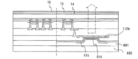
続いて、第2の層間絶縁膜109を選択的にエッチングし、コンタクトホールを形成する。その後、配線108fと接続するための配線111を形成する。また、配線111と同時に画素電極112aを形成する(図6(B))。配線111および画素電極112aは、Al、Ni、W、Mo、Ti、Pt、Cu、Ta、Au、Mnから選ばれた一種の元素または該元素を複数含む合金からなる単層または積層構造を用いて形成することができる。本実施の形態では、Al合金を用いればよく、ここではAl−Ni−Cによって形成する。
Subsequently, the second
次に、第2の層間絶縁膜109、配線111および画素電極112a上に画素電極112bを形成する(図6(C))。画素電極112bは、少なくとも配線111および画素電極112aと重ならない領域119において、第二の層間絶縁膜109と接するように形成する。本実施の形態において、画素電極112a、画素電極112bは透明性導電膜で形成する。例えば、インジウム錫酸化物(ITO、Indium Tin Oxide)、酸化亜鉛(ZnO)、酸化インジウム酸化亜鉛(IZO、Indium Zinc Oxide)、ガリウムを添加した酸化亜鉛(GZO)などその他の透光性酸化物導電材料を用いることが可能である。ITO及び酸化珪素を含むインジウム錫酸化物(ITSO)や、酸化珪素を含んだ酸化インジウムにさらに2〜20wt%の酸化亜鉛(ZnO)を混合したターゲットを用いて形成されたものを用いても良い。
Next, the
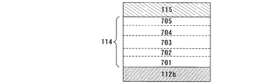
次に、画素電極112a、112bの端部を覆うように絶縁膜(隔壁、バンク)116を形成し、画素電極112bに接するように発光層114を形成する。発光層114は発光物質を含む層であり、例えば、正孔注入層701、正孔輸送層702、発光層703、電子輸送層704、電子注入層705とを有している(図7)。なお、発光層114は必ずしもこの構成に限定されない。少なくとも発光層を有する単層又は積層構造を有する。図7に、画素電極112bと電極115とに挟まれた正孔注入層701、正孔輸送層702、発光層703、電子輸送層704、電子注入層705とを有する発光層114の断面の模式図を示す。
Next, an insulating film (a partition wall or a bank) 116 is formed so as to cover end portions of the
正孔注入層701には、正孔輸送性を有し、なおかつイオン化ポテンシャルが比較的小さく、正孔注入性が高い材料を用いるのが望ましい。大別すると金属酸化物、低分子系有機化合物、および高分子系有機化合物に分けられる。金属酸化物であれば、例えば、酸化バナジウム、酸化モリブデン、酸化ルテニウム、酸化アルミニウムなど用いることができる。低分子系有機化合物あれば、例えば、m−MTDATAに代表されるスターバースト型アミン、銅フタロシアニン(略称:Cu−Pc)に代表される金属フタロシアニン、フタロシアニン(略称:H2−Pc)、2,3−ジオキシエチレンチオフェン誘導体などを用いることができる。低分子系有機化合物と上記金属酸化物とを共蒸着させた膜であっても良い。高分子系有機化合物であれば、例えば、ポリアニリン(略称:PAni)、ポリビニルカルバゾール(略称:PVK)、ポリチオフェン誘導体などの高分子を用いることができる。ポリチオフェン誘導体の一つであるポリエチレンジオキシチオフェン(略称:PEDOT)にポリスチレンスルホン酸(略称:PSS)をドープしたものを用いても良い。また、ベンゾオキサゾール誘導体と、TCQn、FeCl3、C60またはF4TCNQのいずれか一または複数の材料とを併せて用いても良い。
For the
正孔輸送層702には、正孔輸送性が高く、結晶性の低い公知の材料を用いることが望ましい。例えば、芳香族アミン系(すなわち、ベンゼン環−窒素の結合を有するもの)の化合物が好適であり、例えば、4,4’−ビス[N−(3−メチルフェニル)−N−フェニルアミノ]ビフェニル(TPD)や、その誘導体である4,4’−ビス[N−(1−ナフチル)−N−フェニル−アミノ]ビフェニル(α−NPD)などがある。4,4’,4’’−トリス(N,N−ジフェニルアミノ)トリフェニルアミン(TDATA)や、MTDATAなどのスターバースト型芳香族アミン化合物も用いることができる。また4,4’,4’’−トリス(N−カルバゾリル)トリフェニルアミン(略称:TCTA)を用いても良い。また高分子材料としては、良好な正孔輸送性を示すポリ(ビニルカルバゾール)などを用いることができる。
For the hole-
発光層703には、イオン化ポテンシャルが大きく、かつバンドギャップの大きな材料を用いるのが望ましい。例えば、トリス(8−キノリノラト)アルミニウム(Alq3)、トリス(4−メチル−8−キノリノラト)アルミニウム(Almq3)、ビス(10−ヒドロキシベンゾ[η]−キノリナト)ベリリウム(BeBq2)、ビス(2−メチル−8−キノリノラト)−(4−ヒドロキシ−ビフェニリル)−アルミニウム(BAlq)、ビス[2−(2−ヒドロキシフェニル)−ベンゾオキサゾラト]亜鉛(Zn(BOX)2)、ビス[2−(2−ヒドロキシフェニル)−ベンゾチアゾラト]亜鉛(Zn(BTZ)2)などの金属錯体を用いることができる。また、各種蛍光色素(クマリン誘導体、キナクリドン誘導体、ルブレン、4,4−ジシアノメチレン、1−ピロン誘導体、スチルベン誘導体、各種縮合芳香族化合物など)も用いることができる。白金オクタエチルポルフィリン錯体、トリス(フェニルピリジン)イリジウム錯体、トリス(ベンジリデンアセトナート)フェナントレンユーロピウム錯体などの燐光材料も用いることができる。
For the light-emitting
また、発光層703に用いるホスト材料としては、上述した例に代表されるホール輸送材料や電子輸送材料を用いることができる。また、4,4’−N,N’−ジカルバゾリルビフェニル(略称:CBP)などのバイポーラ性の材料も用いることができる。
As a host material used for the light-emitting
電子輸送層704には、電子輸送性の高い材料を用いることが望ましい。例えば、Alq3に代表されるような、キノリン骨格またはベンゾキノリン骨格を有する金属錯体やその混合配位子錯体などを用いることができる。具体的には、Alq3、Almq3、BeBq2、BAlq、Zn(BOX)2、Zn(BTZ)2などの金属錯体が挙げられる。さらに、金属錯体以外にも、2−(4−ビフェニリル)−5−(4−tert−ブチルフェニル)−1,3,4−オキサジアゾール(PBD)、1,3−ビス[5−(p−tert−ブチルフェニル)−1,3,4−オキサジアゾール−2−イル]ベンゼン(OXD−7)などのオキサジアゾール誘導体、3−(4−tert−ブチルフェニル)−4−フェニル−5−(4−ビフェニリル)−1,2,4−トリアゾール(TAZ)、3−(4−tert−ブチルフェニル)−4−(4−エチルフェニル)−5−(4−ビフェニリル)−1,2,4−トリアゾール(p−EtTAZ)などのトリアゾール誘導体、TPBIのようなイミダゾール誘導体、バソフェナントロリン(BPhen)、バソキュプロイン(BCP)などのフェナントロリン誘導体を用いることができる。
It is desirable to use a material having a high electron transporting property for the
電子注入層705には、電子注入性の高い材料を用いるのが望ましい。例えば、LiF、CsFなどのアルカリ金属ハロゲン化物や、CaF2のようなアルカリ土類ハロゲン化物、Li2Oなどのアルカリ金属酸化物のような絶縁体の超薄膜がよく用いられる。また、リチウムアセチルアセトネート(略称:Li(acac))や8−キノリノラト−リチウム(略称:Liq)などのアルカリ金属錯体も有効である。また、モリブデン酸化物(MoOx)やバナジウム酸化物(VOx)、ルテニウム酸化物(RuOx)、タングステン酸化物(WOx)等の金属酸化物またはベンゾオキサゾール誘導体と、アルカリ金属、アルカリ土類金属、または遷移金属のいずれか一または複数の材料とを含むようにしても良い。また酸化チタンを用いていても良い。
For the
なお、発光層114は、必ずしもこれらの層を全て有している必要はない。本実施の形態では、少なくとも発光層703を有していれば良い。また必ずしも発光層703からのみ発光が得られるわけではなく、他の層に用いられる材料の組み合わせによっては、発光層703以外の層から発光が得られる場合もある。また、発光層703と電子輸送層704の間に正孔ブロック層を設けても良い。
Note that the light-emitting
なお色によっては、燐光材料の方が蛍光材料よりも、駆動電圧を低くすることができ、信頼性も高い場合がある。そこで、三原色の各色に対応する発光素子を用いて、フルカラーの表示を行なう場合は、蛍光材料を用いた発光素子と、燐光材料を用いた発光素子とを組み合わせて、各色の発光素子における劣化の度合いを揃えるようにしても良い。 Note that depending on the color, the phosphorescent material can have a lower driving voltage and higher reliability than the fluorescent material. Therefore, when full-color display is performed using light-emitting elements corresponding to the three primary colors, a combination of a light-emitting element using a fluorescent material and a light-emitting element using a phosphorescent material can reduce the deterioration of the light-emitting element of each color. You may make it arrange | equalize a degree.
なお発光層114のうち、電極115に最も近い層(本実施の形態では電子注入層705)に、エッチングされにくい材料を用いることで、発光層114上に電極115をスパッタ法で形成する際に、電極115に最も近い層(本実施の形態では電子注入層705)に与えられるスパッタダメージを軽減させることができる。エッチングされにくい材料とは、例えばモリブデン酸化物(MoOx)やバナジウム酸化物(VOx)、ルテニウム酸化物(RuOx)、タングステン酸化物(WOx)等の金属酸化物、またはベンゾオキサゾール誘導体を用いることができる。これらは蒸着法によって形成されることが好ましい。上記構成により、電極115をスパッタ法で形成した場合でも、発光層114が有する有機物を含む層への、スパッタダメージを抑えることができ、電極115を形成するための物質の選択性が広がる。
Note that a material that is difficult to be etched is used for the
その後、発光層114に接するように電極115を積層して形成する(図6(D))。本実施の形態において、電極115は反射性を有する導電膜で形成する。また、電極115は陰極として用いられるため、仕事関数の小さい金属、合金、電気伝導性化合物、およびこれらの混合物などを用いる。例えば、LiやCs等のアルカリ金属、およびMg、Ca、Sr等のアルカリ土類金属、これらを含む合金(Mg:Ag、Al:Li、Mg:Inなど)、およびこれらの化合物(CaF2、CaN)の他、YbやEr等の希土類金属を用いることができる。また電子注入層を設ける場合、Alなどの他の導電膜を用いることも可能である。
After that, an
その後、電極115上にマスクを用いた蒸着法またはスパッタ法により保護層を形成してもよい。保護層は、電極115を保護するものである。なお、必要でなければ必ずしも設ける必要はない。
Thereafter, a protective layer may be formed on the
次いで、封止基板601をシール材で貼り合わせて発光素子を封止する。表示装置は、表示領域の外周をシール材で囲まれ、一対の基板100、及び封止基板601で封止される。なお、シール材で囲まれた領域には充填材602を充填する。或いは、シール材で囲まれた領域には乾燥した不活性ガスを充填する(図6(D))。
Next, the sealing
次に、電極115が形成されている側とは反対側の基板100上に反射偏光板14、1/4波長板15、偏光板16を順次積層する(図8)。本実施の形態において、反射偏光板として直線偏光反射偏光板を用いる場合、反射偏光板14の透過軸と1/4波長板15の遅相軸とは45°若しくは135°の角度をなすように配置する。
Next, the reflective
上記構成を有する表示装置において、画素電極112bと電極115との間に電圧を印加し、発光層114に順方向バイアスの電流を供給することで、発光層114から光を発生させ、該光を画素電極112b側から取り出すことができる。
In the display device having the above structure, by applying a voltage between the
以上の工程により、図8に示す表示装置を作製することができる。本実施の形態の表示装置において、反射偏光板14上での外光の反射による外部の映像の映り込みを抑え、画像の表示特性を向上させることが可能となる。また、発光層114において発光した光を効率よく取り出すことができ、表示画像の明るさの改善を図ることが可能となる。
Through the above process, the display device illustrated in FIG. 8 can be manufactured. In the display device of the present embodiment, reflection of external video due to reflection of external light on the reflective
(実施の形態6)
本実施の形態において、実施の形態5に示した表示装置のパネルについて、図9を用いて説明する。
(Embodiment 6)
In this embodiment mode, a panel of the display device described in Embodiment Mode 5 will be described with reference to FIGS.
基板50上には、発光素子を含む画素を複数有する表示領域51、ゲートドライバ52、53、ソースドライバ54および接続フィルム55が設けられる(図9(A))。接続フィルム55はICチップなどに接続する。
A
図9(B)はパネルのABを結ぶ破線における断面図を示し、表示領域51に設けられたトランジスタ412、発光素子413および容量素子416、ソースドライバ54に設けられた素子群410を示す。
FIG. 9B is a cross-sectional view taken along a broken line connecting AB of the panel, and shows a
表示領域51、ゲートドライバ52、53およびソースドライバ54の周囲にはシール材408が設けられ、発光素子413は、該シール材408と対向基板406により封止される。この封止処理は、発光素子413を水分から保護するための処理であり、ここではカバー材(ガラス、セラミックス、プラスチック、金属等)により封止する方法を用いるが、熱硬化性樹脂や紫外光硬化性樹脂を用いて封止する方法、金属酸化物や窒化物等のバリア能力が高い薄膜により封止する方法を用いてもよい。基板50上に形成される素子は、非晶質半導体に比べて移動度等の特性が良好な結晶質半導体(ポリシリコン)により形成することが好適であり、そうすると、同一表面上におけるモノリシック化が実現される。上記構成を有するパネルは、接続する外部ICの個数が減少するため、小型・軽量・薄型が実現される。なお、本実施の形態において、基板50の発光素子413が形成された側とは反対側の表面に、反射偏光板14、1/4波長板15、偏光板16とが順に積層して形成されている。
A
なお、表示領域51は絶縁表面上に形成された非晶質半導体(アモルファスシリコン)をチャネル部としたトランジスタにより構成し、表示領域51を制御する回路はICチップにより構成してもよい。非晶質半導体は、CVD法を用いることで、大面積の基板に簡単に形成することができ、かつ結晶化の工程が不要であることから、安価なパネルの提供を可能とする。また、この際、インクジェット法に代表される液滴吐出法により導電層を形成すると、より安価なパネルの提供を可能とする。また、ICチップは、COG(Chip On Glass)方式により基板50上に貼り合わせたり、基板50に接続する接続フィルム55に貼り合わせたりしてもよい。
Note that the
ここで、図10(A)、図10(B)に、チップ状のIC(ICチップ)を、画素を複数有する表示領域が形成された素子基板に実装する様子を示す。図10(A)では、基板50上に表示領域51と、ゲートドライバ52、53とが形成されている。そして、ICチップ58に形成されたソースドライバが、基板50に実装されている。具体的には、ICチップ58に形成されたソースドライバが、基板50に貼り合わされ、表示領域51と電気的に接続されている。また、表示領域51と、ゲートドライバ52、53と、ICチップ58に形成されたソースドライバとに、それぞれ電源電位、各種信号等が、接続フィルム55を介して供給される。
Here, FIGS. 10A and 10B show a state where a chip-like IC (IC chip) is mounted on an element substrate over which a display region having a plurality of pixels is formed. In FIG. 10A, a
図10(B)では、基板50上に表示領域51と、ゲートドライバ52、53とが形成されている。そして、ICチップ59に形成されたソースドライバが、基板50に実装された接続フィルム55に更に実装されている。表示領域51と、ゲートドライバ52と、ICチップ59に形成されたソースドライバとに、それぞれ電源電位、各種信号等が、接続フィルム55を介して供給される。
In FIG. 10B, a
ICチップの実装方法は、特に限定されるものではなく、公知のCOG方法やワイヤボンディング方法、或いはTAB方法などを用いることができる。またICチップを実装する位置は、電気的な接続が可能であるならば、図10に示した位置に限定されない。また、図10ではソースドライバのみをICチップで形成した例について示したが、ゲートドライバをICチップで形成しても良いし、またコントローラ、CPU、メモリ等をICチップで形成し、実装するようにしても良い。また、ソースドライバやゲートドライバ全体をICチップで形成するのではなく、各駆動回路を構成している回路の一部だけを、ICチップで形成するようにしても良い。 The IC chip mounting method is not particularly limited, and a known COG method, wire bonding method, TAB method, or the like can be used. Further, the position where the IC chip is mounted is not limited to the position shown in FIG. 10 as long as electrical connection is possible. Further, although FIG. 10 shows an example in which only the source driver is formed with an IC chip, the gate driver may be formed with an IC chip, and the controller, CPU, memory, etc. may be formed with an IC chip and mounted. Anyway. Further, instead of forming the entire source driver or gate driver with an IC chip, only a part of the circuits constituting each driving circuit may be formed with an IC chip.
なお、駆動回路などの集積回路を別途ICチップで形成して実装することで、全ての回路を画素部と同じ基板上に形成する場合に比べて、歩留まりを高めることができ、また各回路の特性に合わせたプロセスの最適化を容易に行うことができる。 Note that by separately forming and mounting an integrated circuit such as a driver circuit using an IC chip, the yield can be increased as compared with the case where all the circuits are formed over the same substrate as the pixel portion. The process can be easily optimized according to the characteristics.
なお図10では示していないが、表示領域が形成されている基板上に、保護回路を設けていても良い。保護回路により放電経路を確保することができるので、信号及び電源電圧が有する雑音や、何らかの理由によって絶縁膜にチャージングされた電荷によって、基板に形成された半導体素子が劣化あるいは絶縁破壊されるのを防ぐことができる。具体的に図10(A)の場合、接続フィルム55と表示領域51とを電気的に接続している配線に、保護回路を接続することができる。またさらに、接続フィルム55とソースドライバが形成されたICチップ58とを電気的に接続している配線、接続フィルム55とゲートドライバ52、53とを電気的に接続している配線、ソースドライバが形成されたICチップ58と表示領域51とを電気的に接続している配線(ソース線)、ゲートドライバ52、53と表示領域51とを電気的に接続している配線(ゲート線)に、それぞれ保護回路を接続することができる。
Note that although not shown in FIG. 10, a protective circuit may be provided over a substrate over which a display region is formed. Since the discharge path can be secured by the protection circuit, the semiconductor element formed on the substrate is deteriorated or broken down due to noise of the signal and the power supply voltage or charge charged to the insulating film for some reason. Can be prevented. Specifically, in the case of FIG. 10A, a protective circuit can be connected to the wiring that electrically connects the
本実施の形態の表示装置において、反射偏光板14上での外光の反射による外部の映像の映り込みを抑え、画像の表示特性を向上させることが可能となる。また、発光素子413において発光した光を効率よく取り出すことができ、表示画像の明るさの改善を図ることが可能となる。
In the display device of the present embodiment, reflection of external video due to reflection of external light on the reflective
(実施の形態7)
本実施の形態は、実施の形態1〜6に示した表示装置を含む電子機器の一例を図11を参照して説明する。
(Embodiment 7)
In this embodiment, an example of an electronic device including the display device described in any of Embodiments 1 to 6 will be described with reference to FIGS.
図11(A)に示すテレビジョンは、本体8001、表示部8002等を含んでいる。表示部8002は、反射偏光板と1/4波長板と偏光板とを有する表示装置を有している。該表示装置を有する表示部8002を備えることにより、外部の映像の映り込みを抑え、画像の表示特性を向上させたテレビジョンを提供することが可能となる。また、発光層において発光した光を効率よく取り出すことができ、表示画像の明るさが向上したテレビジョンを提供することが可能となる。
A television shown in FIG. 11A includes a main body 8001, a
図11(B)に示す情報端末機器は、本体8101、表示部8102等を含んでいる。表示部8102は、反射偏光板と1/4波長板と偏光板とを有する表示装置を有している。該表示装置を有する表示部8102を備えることにより、外部の映像の映り込みを抑え、画像の表示特性を向上させた情報端末機器を提供することが可能となる。また、発光層において発光した光を効率よく取り出すことができ、表示画像の明るさが向上した情報端末機器を提供することが可能となる。
An information terminal device illustrated in FIG. 11B includes a
図11(C)に示すビデオカメラは、本体8201、表示部8202等を含んでいる。表示部8202は、反射偏光板と1/4波長板と偏光板とを有する表示装置を有している。該表示装置を有する表示部8202を備えることにより、外部の映像の映り込みを抑え、画像の表示特性を向上させたビデオカメラを提供することが可能となる。また、発光層において発光した光を効率よく取り出すことができ、表示画像の明るさが向上したビデオカメラを提供することが可能となる。
A video camera shown in FIG. 11C includes a
図11(D)に示す電話機は、本体8301、表示部8302等を含んでいる。表示部8302は、反射偏光板と1/4波長板と偏光板とを有する表示装置を有している。該表示装置を有する表示部8302を備えることにより、外部の映像の映り込みを抑え、画像の表示特性を向上させた電話機を提供することが可能となる。また、発光層において発光した光を効率よく取り出すことができ、表示画像の明るさが向上した電話機を提供することが可能となる。
A telephone shown in FIG. 11D includes a
図11(E)に示す携帯型のテレビジョンは、本体8401、表示部8402等を含んでいる。表示部8402は、反射偏光板と1/4波長板と偏光板とを有する表示装置を有している。該表示装置を有する表示部8402を備えることにより、外部の映像の映り込みを抑え、画像の表示特性を向上させた携帯型のテレビジョンを提供することが可能となる。また、発光層において発光した光を効率よく取り出すことができ、表示画像の明るさが向上した携帯型のテレビジョンを提供することが可能となる。またテレビジョンとしては、携帯電話機などの携帯端末に搭載する小型のものから、持ち運びをすることができる中型のもの、また、大型のもの(例えば40インチ以上)まで、幅広いものに、本発明の表示装置を適用することができる。
A portable television shown in FIG. 11E includes a
なお、本発明に係る電子機器は、図11(A)〜(E)に限定されず、表示部に反射偏光板と1/4波長板と偏光板とを有する表示装置を有するものが含まれる。 In addition, the electronic device which concerns on this invention is not limited to FIG. 11 (A)-(E), The thing which has a display apparatus which has a reflective polarizing plate, a quarter wavelength plate, and a polarizing plate in a display part is contained. .
このように、反射偏光板と1/4波長板と偏光板とを有する表示装置を有する表示部等を備えることで、外部の映像の映り込みを抑え、画像の表示特性を向上させた電子機器を提供することが可能となる。また、発光層において発光した光を効率よく取り出すことができ、表示画像の明るさが向上した電子機器を提供することが可能となる。 As described above, an electronic apparatus that includes a display unit having a display device having a reflective polarizing plate, a quarter-wave plate, and a polarizing plate to suppress reflection of an external image and improve image display characteristics. Can be provided. In addition, light emitted from the light-emitting layer can be extracted efficiently, and an electronic device with improved brightness of a display image can be provided.
11 透明電極
12 発光層
13 反射性電極
14 反射偏光板
15 波長板
16 偏光板
100 基板
DESCRIPTION OF
Claims (7)
前記第1の1/4波長板上に設けられた第1の反射偏光板と、
前記第1の反射偏光板上に設けられた透明基板と、
前記透明基板上に設けられた第1の透明電極と、
前記第1の透明電極上に設けられた発光層と、
前記発光層上に設けられた第2の透明電極と、
前記第2の透明電極上に設けられた第2の反射偏光板と、
前記第2の反射偏光板上に設けられた第2の1/4波長板と、
前記第2の1/4波長板上に設けられた第2の吸収偏光板と、
前記第2の透明電極と前記第2の反射偏光板との間に、膜中に前記膜とは屈折率の異なる複数の大きさの異なる粒子を拡散させた散乱層と、を有し、
前記第1の反射偏光板と前記第2の反射偏光板は直線偏光板であり、
前記第1の吸収偏光板の透過軸と前記第1の1/4波長板の遅相軸は45°の角度であり、
前記第1の吸収偏光板の透過軸と前記第1の反射偏光板の透過軸は平行であり、
前記第2の吸収偏光板の透過軸と前記第2の1/4波長板の遅相軸は45°の角度であり、
前記第2の吸収偏光板の透過軸と前記第2の反射偏光板の透過軸は平行であり、
前記第1の吸収偏光板の吸収軸と前記第2の吸収偏光板の吸収軸は直交していることを特徴とする表示装置。 A first quarter wave plate provided on the first absorbing polarizer;
A first reflective polarizing plate provided on the first quarter-wave plate;
A transparent substrate provided on the first reflective polarizing plate;
A first transparent electrode provided on the transparent substrate;
A light emitting layer provided on the first transparent electrode;
A second transparent electrode provided on the light emitting layer;
A second reflective polarizing plate provided on the second transparent electrode;
A second quarter-wave plate provided on the second reflective polarizing plate;
A second absorbing polarizer provided on the second quarter-wave plate;
Between the second transparent electrode and the second reflective polarizing plate, a scattering layer in which a plurality of different particles having different refractive indexes from the film are diffused in the film ,
The first reflective polarizer and the second reflective polarizer are linear polarizers,
The transmission axis of the first absorption polarizing plate and the slow axis of the first quarter-wave plate are at an angle of 45 °,
The transmission axis of the first absorption polarizer and the transmission axis of the first reflection polarizer are parallel,
The transmission axis of the second absorption polarizing plate and the slow axis of the second quarter-wave plate are at an angle of 45 °,
The transmission axis of the second absorption polarizer and the transmission axis of the second reflection polarizer are parallel,
The display device, wherein an absorption axis of the first absorption polarizing plate and an absorption axis of the second absorption polarizing plate are orthogonal to each other.
前記第1の1/4波長板上に設けられた第1の反射偏光板と、
前記第1の反射偏光板上に設けられた透明基板と、
前記透明基板上に設けられた第1の透明電極と、
前記第1の透明電極上に設けられた発光層と、
前記発光層上に設けられた第2の透明電極と、
前記第2の透明電極上に設けられた第2の反射偏光板と、
前記第2の反射偏光板上に設けられた第2の1/4波長板と、
前記第2の1/4波長板上に設けられた第2の吸収偏光板と、
前記第2の透明電極と前記第2の反射偏光板との間に、膜中に前記膜とは屈折率の異なる複数の大きさの異なる粒子を拡散させた散乱層と、を有し、
前記第1の反射偏光板と前記第2の反射偏光板は円偏光板であり、
前記第1の反射偏光板のらせんの回転方向と前記第2の反射偏光板のらせんの回転方向は逆向きであることを特徴とする表示装置。 A first quarter wave plate provided on the first absorbing polarizer;
A first reflective polarizing plate provided on the first quarter-wave plate;
A transparent substrate provided on the first reflective polarizing plate;
A first transparent electrode provided on the transparent substrate;
A light emitting layer provided on the first transparent electrode;
A second transparent electrode provided on the light emitting layer;
A second reflective polarizing plate provided on the second transparent electrode;
A second quarter-wave plate provided on the second reflective polarizing plate;
A second absorbing polarizer provided on the second quarter-wave plate;
Between the second transparent electrode and the second reflective polarizing plate, a scattering layer in which a plurality of different particles having different refractive indexes from the film are diffused in the film ,
The first reflective polarizer and the second reflective polarizer are circular polarizers,
The display device according to claim 1, wherein the spiral direction of the first reflective polarizer and the spiral direction of the second reflective polarizer are opposite to each other.
前記第1の1/4波長板上に設けられた第1の反射偏光板と、
前記第1の反射偏光板上に設けられた透明基板と、
前記透明基板上に設けられた、ソース領域又はドレイン領域を有する半導体膜を有する薄膜トランジスタと、
前記薄膜トランジスタ上に設けられた、前記ソース領域又はドレイン領域に達するコンタクトホールを有する層間絶縁膜と、
前記層間絶縁膜上に設けられた前記ソース領域又はドレイン領域と電気的に接続された配線と、
前記層間絶縁膜及び前記配線上に設けられた第1の透明電極と、
前記第1の透明電極上に設けられた発光層と、
前記発光層上に設けられた第2の透明電極と、
前記第2の透明電極上に設けられた第2の反射偏光板と、
前記第2の反射偏光板上に設けられた第2の1/4波長板と、
前記第2の1/4波長板上に設けられた第2の吸収偏光板と、
前記第2の透明電極と前記第2の反射偏光板との間に、膜中に前記膜とは屈折率の異なる複数の大きさの異なる粒子を拡散させた散乱層と、を有し、
前記第1の反射偏光板と前記第2の反射偏光板は直線偏光板であり、
前記第1の吸収偏光板の透過軸と前記第1の1/4波長板の遅相軸は45°の角度であり、
前記第1の吸収偏光板の透過軸と前記第1の反射偏光板の透過軸は平行であり、
前記第2の吸収偏光板の透過軸と前記第2の1/4波長板の遅相軸は45°の角度であり、
前記第2の吸収偏光板の透過軸と前記第2の反射偏光板の透過軸は平行であり、
前記第1の吸収偏光板の吸収軸と前記第2の吸収偏光板の吸収軸は直交していることを特徴とする表示装置。 A first quarter wave plate provided on the first absorbing polarizer;
A first reflective polarizing plate provided on the first quarter-wave plate;
A transparent substrate provided on the first reflective polarizing plate;
A thin film transistor having a semiconductor film having a source region or a drain region provided on the transparent substrate;
An interlayer insulating film provided on the thin film transistor and having a contact hole reaching the source region or the drain region;
A wiring electrically connected to the source region or the drain region provided on the interlayer insulating film;
A first transparent electrode provided on the interlayer insulating film and the wiring;
A light emitting layer provided on the first transparent electrode;
A second transparent electrode provided on the light emitting layer;
A second reflective polarizing plate provided on the second transparent electrode;
A second quarter-wave plate provided on the second reflective polarizing plate;
A second absorbing polarizer provided on the second quarter-wave plate;
Between the second transparent electrode and the second reflective polarizing plate, a scattering layer in which a plurality of different particles having different refractive indexes from the film are diffused in the film ,
The first reflective polarizer and the second reflective polarizer are linear polarizers,
The transmission axis of the first absorption polarizing plate and the slow axis of the first quarter-wave plate are at an angle of 45 °,
The transmission axis of the first absorption polarizer and the transmission axis of the first reflection polarizer are parallel,
The transmission axis of the second absorption polarizing plate and the slow axis of the second quarter-wave plate are at an angle of 45 °,
The transmission axis of the second absorption polarizer and the transmission axis of the second reflection polarizer are parallel,
The display device, wherein an absorption axis of the first absorption polarizing plate and an absorption axis of the second absorption polarizing plate are orthogonal to each other.
前記第1の1/4波長板上に設けられた第1の反射偏光板と、
前記第1の反射偏光板上に設けられた透明基板と、
前記透明基板上に設けられた、ソース領域又はドレイン領域を有する半導体膜を有する薄膜トランジスタと、
前記薄膜トランジスタ上に設けられた、前記ソース領域又はドレイン領域に達するコンタクトホールを有する層間絶縁膜と、
前記層間絶縁膜上に設けられた前記ソース領域又はドレイン領域と電気的に接続された配線と、
前記層間絶縁膜及び前記配線上に設けられた第1の透明電極と、
前記第1の透明電極上に設けられた発光層と、
前記発光層上に設けられた第2の透明電極と、
前記第2の透明電極上に設けられた第2の反射偏光板と、
前記第2の反射偏光板上に設けられた第2の1/4波長板と、
前記第2の1/4波長板上に設けられた第2の吸収偏光板と、
前記第2の透明電極と前記第2の反射偏光板との間に、膜中に前記膜とは屈折率の異なる複数の大きさの異なる粒子を拡散させた散乱層と、を有し、
前記第1の反射偏光板と前記第2の反射偏光板は円偏光板であり、
前記第1の反射偏光板のらせんの回転方向と前記第2の反射偏光板のらせんの回転方向は逆向きであることを特徴とする表示装置。 A first quarter wave plate provided on the first absorbing polarizer;
A first reflective polarizing plate provided on the first quarter-wave plate;
A transparent substrate provided on the first reflective polarizing plate;
A thin film transistor having a semiconductor film having a source region or a drain region provided on the transparent substrate;
An interlayer insulating film provided on the thin film transistor and having a contact hole reaching the source region or the drain region;
A wiring electrically connected to the source region or the drain region provided on the interlayer insulating film;
A first transparent electrode provided on the interlayer insulating film and the wiring;
A light emitting layer provided on the first transparent electrode;
A second transparent electrode provided on the light emitting layer;
A second reflective polarizing plate provided on the second transparent electrode;
A second quarter-wave plate provided on the second reflective polarizing plate;
A second absorbing polarizer provided on the second quarter-wave plate;
Between the second transparent electrode and the second reflective polarizing plate, a scattering layer in which a plurality of different particles having different refractive indexes from the film are diffused in the film ,
The first reflective polarizer and the second reflective polarizer are circular polarizers,
The display device according to claim 1, wherein the spiral direction of the first reflective polarizer and the spiral direction of the second reflective polarizer are opposite to each other.
前記第2の透明電極と前記第2の反射偏光板との間に第3の1/4波長板が形成されてなることを特徴とする表示装置。 In any one of Claims 1 thru | or 4 ,
A display device, wherein a third quarter-wave plate is formed between the second transparent electrode and the second reflective polarizing plate.
前記第1の1/4波長板又は前記第2の1/4波長板の少なくとも一方は、可視光の範囲において1/4波長板としての効果を有する広帯域化1/4波長板であることを特徴とする表示装置。 In any one of Claims 1 thru | or 5 ,
At least one of the first quarter wavelength plate or the second quarter wavelength plate is a broadband quarter wavelength plate having an effect as a quarter wavelength plate in a visible light range. Characteristic display device.
Priority Applications (1)
| Application Number | Priority Date | Filing Date | Title |
|---|---|---|---|
| JP2006282392A JP5250196B2 (en) | 2005-10-18 | 2006-10-17 | Display device and electronic device |
Applications Claiming Priority (3)
| Application Number | Priority Date | Filing Date | Title |
|---|---|---|---|
| JP2005303770 | 2005-10-18 | ||
| JP2005303770 | 2005-10-18 | ||
| JP2006282392A JP5250196B2 (en) | 2005-10-18 | 2006-10-17 | Display device and electronic device |
Related Child Applications (1)
| Application Number | Title | Priority Date | Filing Date |
|---|---|---|---|
| JP2011195621A Division JP5288652B2 (en) | 2005-10-18 | 2011-09-08 | Electronics |
Publications (3)
| Publication Number | Publication Date |
|---|---|
| JP2007141824A JP2007141824A (en) | 2007-06-07 |
| JP2007141824A5 JP2007141824A5 (en) | 2010-04-22 |
| JP5250196B2 true JP5250196B2 (en) | 2013-07-31 |
Family
ID=38204412
Family Applications (1)
| Application Number | Title | Priority Date | Filing Date |
|---|---|---|---|
| JP2006282392A Expired - Fee Related JP5250196B2 (en) | 2005-10-18 | 2006-10-17 | Display device and electronic device |
Country Status (1)
| Country | Link |
|---|---|
| JP (1) | JP5250196B2 (en) |
Families Citing this family (15)
| Publication number | Priority date | Publication date | Assignee | Title |
|---|---|---|---|---|
| US8217572B2 (en) * | 2005-10-18 | 2012-07-10 | Semiconductor Energy Laboratory Co., Ltd. | Display device with prism layer |
| KR101463024B1 (en) | 2007-02-15 | 2014-11-18 | 엘지디스플레이 주식회사 | Flat panel display device |
| KR101106294B1 (en) * | 2008-05-22 | 2012-01-18 | 주식회사 엘지화학 | Polarizer for oeld having improved brightness |
| US8198802B2 (en) | 2008-07-25 | 2012-06-12 | Samsung Mobile Display Co., Ltd. | Organic light emitting diode display for suppressing reflection of external light |
| JP4938047B2 (en) * | 2008-08-19 | 2012-05-23 | 三星モバイルディスプレイ株式會社 | Organic light emitting display |
| US8169386B2 (en) | 2008-08-19 | 2012-05-01 | Samsung Mobile Display Co., Ltd. | Organic light emitting diode display |
| KR100965258B1 (en) | 2008-08-27 | 2010-06-22 | 삼성모바일디스플레이주식회사 | Organic light emitting diode display |
| JP2010205506A (en) * | 2009-03-02 | 2010-09-16 | Toppan Printing Co Ltd | El element |
| KR101470811B1 (en) | 2009-09-16 | 2014-12-09 | 가부시키가이샤 한도오따이 에네루기 켄큐쇼 | Semiconductor device |
| KR101094290B1 (en) * | 2010-01-18 | 2011-12-19 | 삼성모바일디스플레이주식회사 | Organic light emitting diode display |
| JP5827885B2 (en) * | 2010-12-24 | 2015-12-02 | 株式会社半導体エネルギー研究所 | Light emitting device and lighting device |
| JP5637027B2 (en) * | 2011-03-22 | 2014-12-10 | 日本ゼオン株式会社 | Lens array sheet and light emitting device |
| KR101883848B1 (en) * | 2011-12-28 | 2018-08-02 | 삼성디스플레이 주식회사 | Organic light emitting display apparatus and the method for manufacturing the same |
| EP2926389B1 (en) * | 2012-11-30 | 2021-03-17 | 3M Innovative Properties Company | Emissive display with reflective polarizer |
| JP6495897B2 (en) * | 2013-06-06 | 2019-04-03 | スリーエム イノベイティブ プロパティズ カンパニー | Anti-reflection OLED structure |
Family Cites Families (4)
| Publication number | Priority date | Publication date | Assignee | Title |
|---|---|---|---|---|
| JP2001357979A (en) * | 2000-06-15 | 2001-12-26 | Toshiba Corp | El element |
| JP2003315548A (en) * | 2002-04-24 | 2003-11-06 | Nitto Denko Corp | Optical element, surface light source device, and liquid crystal display |
| JP4345312B2 (en) * | 2003-01-23 | 2009-10-14 | 日本ゼオン株式会社 | Broadband quarter-wave plate original, broadband circular polarizer original, optical element original, and display device |
| JP4463492B2 (en) * | 2003-04-10 | 2010-05-19 | 株式会社半導体エネルギー研究所 | Manufacturing equipment |
-
2006
- 2006-10-17 JP JP2006282392A patent/JP5250196B2/en not_active Expired - Fee Related
Also Published As
| Publication number | Publication date |
|---|---|
| JP2007141824A (en) | 2007-06-07 |
Similar Documents
| Publication | Publication Date | Title |
|---|---|---|
| JP5288652B2 (en) | Electronics | |
| JP5250196B2 (en) | Display device and electronic device | |
| US10490618B2 (en) | Light emitting device | |
| JP5031115B2 (en) | Display device | |
| JP4711595B2 (en) | EL display and electronic device | |
| US9034675B2 (en) | Light-emitting device and method for manufacturing light-emitting device | |
| JP5663641B2 (en) | Light emitting element | |
| KR101087015B1 (en) | Light-emitting device and electronic device | |
| KR101251622B1 (en) | Light emitting device | |
| US7476908B2 (en) | Light emitting device | |
| JP4684042B2 (en) | LIGHT EMITTING ELEMENT, LIGHT EMITTING DEVICE, AND ELECTRONIC DEVICE | |
| JP2005183006A (en) | Light-emitting device and electronic equipment | |
| JP4754876B2 (en) | Display device and manufacturing method thereof | |
| JP4817730B2 (en) | Display device | |
| JP5255748B2 (en) | LIGHT EMITTING ELEMENT AND LIGHT EMITTING DEVICE | |
| JP2005276620A (en) | Light emitting device, electronic equipment, and television receiver | |
| JP4519538B2 (en) | LIGHT EMITTING DEVICE AND ELECTRONIC DEVICE | |
| JP4704004B2 (en) | LIGHT EMITTING DEVICE AND ELECTRONIC DEVICE | |
| JP5648108B2 (en) | Light emitting device | |
| JP5084123B2 (en) | Light emitting device | |
| JP2006100138A (en) | Display device |
Legal Events
| Date | Code | Title | Description |
|---|---|---|---|
| A621 | Written request for application examination |
Free format text: JAPANESE INTERMEDIATE CODE: A621 Effective date: 20091015 |
|
| A521 | Request for written amendment filed |
Free format text: JAPANESE INTERMEDIATE CODE: A523 Effective date: 20100304 |
|
| A977 | Report on retrieval |
Free format text: JAPANESE INTERMEDIATE CODE: A971007 Effective date: 20110706 |
|
| A131 | Notification of reasons for refusal |
Free format text: JAPANESE INTERMEDIATE CODE: A131 Effective date: 20110712 |
|
| A521 | Request for written amendment filed |
Free format text: JAPANESE INTERMEDIATE CODE: A523 Effective date: 20110908 |
|
| A131 | Notification of reasons for refusal |
Free format text: JAPANESE INTERMEDIATE CODE: A131 Effective date: 20120703 |
|
| A521 | Request for written amendment filed |
Free format text: JAPANESE INTERMEDIATE CODE: A523 Effective date: 20120723 |
|
| TRDD | Decision of grant or rejection written | ||
| A01 | Written decision to grant a patent or to grant a registration (utility model) |
Free format text: JAPANESE INTERMEDIATE CODE: A01 Effective date: 20130409 |
|
| A61 | First payment of annual fees (during grant procedure) |
Free format text: JAPANESE INTERMEDIATE CODE: A61 Effective date: 20130415 |
|
| R150 | Certificate of patent or registration of utility model |
Ref document number: 5250196 Country of ref document: JP Free format text: JAPANESE INTERMEDIATE CODE: R150 Free format text: JAPANESE INTERMEDIATE CODE: R150 |
|
| FPAY | Renewal fee payment (event date is renewal date of database) |
Free format text: PAYMENT UNTIL: 20160419 Year of fee payment: 3 |
|
| R250 | Receipt of annual fees |
Free format text: JAPANESE INTERMEDIATE CODE: R250 |
|
| R250 | Receipt of annual fees |
Free format text: JAPANESE INTERMEDIATE CODE: R250 |
|
| R250 | Receipt of annual fees |
Free format text: JAPANESE INTERMEDIATE CODE: R250 |
|
| R250 | Receipt of annual fees |
Free format text: JAPANESE INTERMEDIATE CODE: R250 |
|
| R250 | Receipt of annual fees |
Free format text: JAPANESE INTERMEDIATE CODE: R250 |
|
| R250 | Receipt of annual fees |
Free format text: JAPANESE INTERMEDIATE CODE: R250 |
|
| LAPS | Cancellation because of no payment of annual fees |