JP4704004B2 - LIGHT EMITTING DEVICE AND ELECTRONIC DEVICE - Google Patents
LIGHT EMITTING DEVICE AND ELECTRONIC DEVICE Download PDFInfo
- Publication number
- JP4704004B2 JP4704004B2 JP2004299587A JP2004299587A JP4704004B2 JP 4704004 B2 JP4704004 B2 JP 4704004B2 JP 2004299587 A JP2004299587 A JP 2004299587A JP 2004299587 A JP2004299587 A JP 2004299587A JP 4704004 B2 JP4704004 B2 JP 4704004B2
- Authority
- JP
- Japan
- Prior art keywords
- light
- layer
- film
- anode
- tft
- Prior art date
- Legal status (The legal status is an assumption and is not a legal conclusion. Google has not performed a legal analysis and makes no representation as to the accuracy of the status listed.)
- Expired - Fee Related
Links
- 230000004888 barrier function Effects 0.000 claims description 68
- 238000002347 injection Methods 0.000 claims description 50
- 239000007924 injection Substances 0.000 claims description 50
- VYPSYNLAJGMNEJ-UHFFFAOYSA-N Silicium dioxide Chemical compound O=[Si]=O VYPSYNLAJGMNEJ-UHFFFAOYSA-N 0.000 claims description 42
- 229910052814 silicon oxide Inorganic materials 0.000 claims description 40
- 229910052581 Si3N4 Inorganic materials 0.000 claims description 28
- HQVNEWCFYHHQES-UHFFFAOYSA-N silicon nitride Chemical compound N12[Si]34N5[Si]62N3[Si]51N64 HQVNEWCFYHHQES-UHFFFAOYSA-N 0.000 claims description 28
- XUIMIQQOPSSXEZ-UHFFFAOYSA-N Silicon Chemical compound [Si] XUIMIQQOPSSXEZ-UHFFFAOYSA-N 0.000 claims description 19
- 229910052710 silicon Inorganic materials 0.000 claims description 19
- 239000010703 silicon Substances 0.000 claims description 19
- IJGRMHOSHXDMSA-UHFFFAOYSA-N Atomic nitrogen Chemical compound N#N IJGRMHOSHXDMSA-UHFFFAOYSA-N 0.000 claims description 9
- 229910052757 nitrogen Inorganic materials 0.000 claims description 7
- AMGQUBHHOARCQH-UHFFFAOYSA-N indium;oxotin Chemical compound [In].[Sn]=O AMGQUBHHOARCQH-UHFFFAOYSA-N 0.000 claims description 6
- 239000010410 layer Substances 0.000 description 302
- 239000010408 film Substances 0.000 description 287
- 239000004065 semiconductor Substances 0.000 description 144
- 239000000463 material Substances 0.000 description 64
- 239000000758 substrate Substances 0.000 description 58
- 238000000034 method Methods 0.000 description 31
- 239000004020 conductor Substances 0.000 description 24
- 239000011229 interlayer Substances 0.000 description 24
- 238000002161 passivation Methods 0.000 description 22
- 239000012535 impurity Substances 0.000 description 17
- 238000005192 partition Methods 0.000 description 15
- 230000005525 hole transport Effects 0.000 description 14
- 238000004519 manufacturing process Methods 0.000 description 14
- 229920005989 resin Polymers 0.000 description 13
- 239000011347 resin Substances 0.000 description 13
- 239000012298 atmosphere Substances 0.000 description 12
- 238000010438 heat treatment Methods 0.000 description 12
- 229910052751 metal Inorganic materials 0.000 description 12
- 239000002184 metal Substances 0.000 description 12
- QVGXLLKOCUKJST-UHFFFAOYSA-N atomic oxygen Chemical compound [O] QVGXLLKOCUKJST-UHFFFAOYSA-N 0.000 description 11
- 229910052760 oxygen Inorganic materials 0.000 description 11
- 239000001301 oxygen Substances 0.000 description 11
- XLOMVQKBTHCTTD-UHFFFAOYSA-N Zinc monoxide Chemical compound [Zn]=O XLOMVQKBTHCTTD-UHFFFAOYSA-N 0.000 description 10
- 230000001681 protective effect Effects 0.000 description 10
- 239000000126 substance Substances 0.000 description 10
- 229910052782 aluminium Inorganic materials 0.000 description 9
- -1 Li and Cs Chemical class 0.000 description 8
- 239000002585 base Substances 0.000 description 8
- 230000006866 deterioration Effects 0.000 description 8
- 238000004544 sputter deposition Methods 0.000 description 8
- 229910052784 alkaline earth metal Inorganic materials 0.000 description 7
- 150000001342 alkaline earth metals Chemical class 0.000 description 7
- 239000003990 capacitor Substances 0.000 description 7
- 239000000969 carrier Substances 0.000 description 7
- 238000002425 crystallisation Methods 0.000 description 7
- 150000002894 organic compounds Chemical class 0.000 description 7
- 230000002829 reductive effect Effects 0.000 description 7
- 239000002356 single layer Substances 0.000 description 7
- UHOVQNZJYSORNB-UHFFFAOYSA-N Benzene Chemical group C1=CC=CC=C1 UHOVQNZJYSORNB-UHFFFAOYSA-N 0.000 description 6
- 229910052783 alkali metal Inorganic materials 0.000 description 6
- 150000001340 alkali metals Chemical class 0.000 description 6
- XAGFODPZIPBFFR-UHFFFAOYSA-N aluminium Chemical compound [Al] XAGFODPZIPBFFR-UHFFFAOYSA-N 0.000 description 6
- QVQLCTNNEUAWMS-UHFFFAOYSA-N barium oxide Chemical compound [Ba]=O QVQLCTNNEUAWMS-UHFFFAOYSA-N 0.000 description 6
- 230000015572 biosynthetic process Effects 0.000 description 6
- 238000010586 diagram Methods 0.000 description 6
- KPUWHANPEXNPJT-UHFFFAOYSA-N disiloxane Chemical class [SiH3]O[SiH3] KPUWHANPEXNPJT-UHFFFAOYSA-N 0.000 description 6
- 238000005259 measurement Methods 0.000 description 6
- 229910018557 Si O Inorganic materials 0.000 description 5
- NIXOWILDQLNWCW-UHFFFAOYSA-N acrylic acid group Chemical group C(C=C)(=O)O NIXOWILDQLNWCW-UHFFFAOYSA-N 0.000 description 5
- 230000008025 crystallization Effects 0.000 description 5
- 238000003795 desorption Methods 0.000 description 5
- 239000000945 filler Substances 0.000 description 5
- 239000000203 mixture Substances 0.000 description 5
- 229920003023 plastic Polymers 0.000 description 5
- 239000004033 plastic Substances 0.000 description 5
- LIVNPJMFVYWSIS-UHFFFAOYSA-N silicon monoxide Inorganic materials [Si-]#[O+] LIVNPJMFVYWSIS-UHFFFAOYSA-N 0.000 description 5
- 239000007858 starting material Substances 0.000 description 5
- XKRFYHLGVUSROY-UHFFFAOYSA-N Argon Chemical compound [Ar] XKRFYHLGVUSROY-UHFFFAOYSA-N 0.000 description 4
- 229910045601 alloy Inorganic materials 0.000 description 4
- 239000000956 alloy Substances 0.000 description 4
- 150000001875 compounds Chemical class 0.000 description 4
- PMHQVHHXPFUNSP-UHFFFAOYSA-M copper(1+);methylsulfanylmethane;bromide Chemical compound Br[Cu].CSC PMHQVHHXPFUNSP-UHFFFAOYSA-M 0.000 description 4
- 230000000694 effects Effects 0.000 description 4
- 230000005684 electric field Effects 0.000 description 4
- 239000011521 glass Substances 0.000 description 4
- 239000001257 hydrogen Substances 0.000 description 4
- 229910052739 hydrogen Inorganic materials 0.000 description 4
- 229910052744 lithium Inorganic materials 0.000 description 4
- 229910044991 metal oxide Inorganic materials 0.000 description 4
- 150000004706 metal oxides Chemical class 0.000 description 4
- 239000011368 organic material Substances 0.000 description 4
- 239000010936 titanium Substances 0.000 description 4
- GYHNNYVSQQEPJS-UHFFFAOYSA-N Gallium Chemical compound [Ga] GYHNNYVSQQEPJS-UHFFFAOYSA-N 0.000 description 3
- UFHFLCQGNIYNRP-UHFFFAOYSA-N Hydrogen Chemical compound [H][H] UFHFLCQGNIYNRP-UHFFFAOYSA-N 0.000 description 3
- 238000000137 annealing Methods 0.000 description 3
- 150000004696 coordination complex Chemical class 0.000 description 3
- 238000007872 degassing Methods 0.000 description 3
- 238000009792 diffusion process Methods 0.000 description 3
- 230000005611 electricity Effects 0.000 description 3
- 229910052733 gallium Inorganic materials 0.000 description 3
- 230000006872 improvement Effects 0.000 description 3
- 239000011261 inert gas Substances 0.000 description 3
- 229910000476 molybdenum oxide Inorganic materials 0.000 description 3
- 238000000059 patterning Methods 0.000 description 3
- 238000005268 plasma chemical vapour deposition Methods 0.000 description 3
- 229920003227 poly(N-vinyl carbazole) Polymers 0.000 description 3
- 229920002620 polyvinyl fluoride Polymers 0.000 description 3
- 238000001552 radio frequency sputter deposition Methods 0.000 description 3
- 229910001925 ruthenium oxide Inorganic materials 0.000 description 3
- WOCIAKWEIIZHES-UHFFFAOYSA-N ruthenium(iv) oxide Chemical compound O=[Ru]=O WOCIAKWEIIZHES-UHFFFAOYSA-N 0.000 description 3
- 229910052709 silver Inorganic materials 0.000 description 3
- 239000010935 stainless steel Substances 0.000 description 3
- 229910001220 stainless steel Inorganic materials 0.000 description 3
- 230000003068 static effect Effects 0.000 description 3
- 229910001935 vanadium oxide Inorganic materials 0.000 description 3
- XLYOFNOQVPJJNP-UHFFFAOYSA-N water Substances O XLYOFNOQVPJJNP-UHFFFAOYSA-N 0.000 description 3
- YVTHLONGBIQYBO-UHFFFAOYSA-N zinc indium(3+) oxygen(2-) Chemical compound [O--].[Zn++].[In+3] YVTHLONGBIQYBO-UHFFFAOYSA-N 0.000 description 3
- 239000011787 zinc oxide Substances 0.000 description 3
- BCMCBBGGLRIHSE-UHFFFAOYSA-N 1,3-benzoxazole Chemical class C1=CC=C2OC=NC2=C1 BCMCBBGGLRIHSE-UHFFFAOYSA-N 0.000 description 2
- STTGYIUESPWXOW-UHFFFAOYSA-N 2,9-dimethyl-4,7-diphenyl-1,10-phenanthroline Chemical compound C=12C=CC3=C(C=4C=CC=CC=4)C=C(C)N=C3C2=NC(C)=CC=1C1=CC=CC=C1 STTGYIUESPWXOW-UHFFFAOYSA-N 0.000 description 2
- UOCMXZLNHQBBOS-UHFFFAOYSA-N 2-(1,3-benzoxazol-2-yl)phenol zinc Chemical compound [Zn].Oc1ccccc1-c1nc2ccccc2o1.Oc1ccccc1-c1nc2ccccc2o1 UOCMXZLNHQBBOS-UHFFFAOYSA-N 0.000 description 2
- ZVFQEOPUXVPSLB-UHFFFAOYSA-N 3-(4-tert-butylphenyl)-4-phenyl-5-(4-phenylphenyl)-1,2,4-triazole Chemical compound C1=CC(C(C)(C)C)=CC=C1C(N1C=2C=CC=CC=2)=NN=C1C1=CC=C(C=2C=CC=CC=2)C=C1 ZVFQEOPUXVPSLB-UHFFFAOYSA-N 0.000 description 2
- DHDHJYNTEFLIHY-UHFFFAOYSA-N 4,7-diphenyl-1,10-phenanthroline Chemical compound C1=CC=CC=C1C1=CC=NC2=C1C=CC1=C(C=3C=CC=CC=3)C=CN=C21 DHDHJYNTEFLIHY-UHFFFAOYSA-N 0.000 description 2
- 239000004925 Acrylic resin Substances 0.000 description 2
- 229920000178 Acrylic resin Polymers 0.000 description 2
- 229910018125 Al-Si Inorganic materials 0.000 description 2
- 229910018520 Al—Si Inorganic materials 0.000 description 2
- 229920002799 BoPET Polymers 0.000 description 2
- 241000284156 Clerodendrum quadriloculare Species 0.000 description 2
- 229910052691 Erbium Inorganic materials 0.000 description 2
- 239000005041 Mylar™ Substances 0.000 description 2
- 229920001609 Poly(3,4-ethylenedioxythiophene) Polymers 0.000 description 2
- 239000004642 Polyimide Substances 0.000 description 2
- 229910004298 SiO 2 Inorganic materials 0.000 description 2
- 229910000577 Silicon-germanium Inorganic materials 0.000 description 2
- 229910006404 SnO 2 Inorganic materials 0.000 description 2
- BOTDANWDWHJENH-UHFFFAOYSA-N Tetraethyl orthosilicate Chemical compound CCO[Si](OCC)(OCC)OCC BOTDANWDWHJENH-UHFFFAOYSA-N 0.000 description 2
- NRTOMJZYCJJWKI-UHFFFAOYSA-N Titanium nitride Chemical compound [Ti]#N NRTOMJZYCJJWKI-UHFFFAOYSA-N 0.000 description 2
- 239000007983 Tris buffer Substances 0.000 description 2
- 229910052769 Ytterbium Inorganic materials 0.000 description 2
- XHCLAFWTIXFWPH-UHFFFAOYSA-N [O-2].[O-2].[O-2].[O-2].[O-2].[V+5].[V+5] Chemical compound [O-2].[O-2].[O-2].[O-2].[O-2].[V+5].[V+5] XHCLAFWTIXFWPH-UHFFFAOYSA-N 0.000 description 2
- LEVVHYCKPQWKOP-UHFFFAOYSA-N [Si].[Ge] Chemical compound [Si].[Ge] LEVVHYCKPQWKOP-UHFFFAOYSA-N 0.000 description 2
- 238000001994 activation Methods 0.000 description 2
- 229910052786 argon Inorganic materials 0.000 description 2
- 238000005452 bending Methods 0.000 description 2
- UFVXQDWNSAGPHN-UHFFFAOYSA-K bis[(2-methylquinolin-8-yl)oxy]-(4-phenylphenoxy)alumane Chemical compound [Al+3].C1=CC=C([O-])C2=NC(C)=CC=C21.C1=CC=C([O-])C2=NC(C)=CC=C21.C1=CC([O-])=CC=C1C1=CC=CC=C1 UFVXQDWNSAGPHN-UHFFFAOYSA-K 0.000 description 2
- DQXBYHZEEUGOBF-UHFFFAOYSA-N but-3-enoic acid;ethene Chemical compound C=C.OC(=O)CC=C DQXBYHZEEUGOBF-UHFFFAOYSA-N 0.000 description 2
- 229910052792 caesium Inorganic materials 0.000 description 2
- 229910052791 calcium Inorganic materials 0.000 description 2
- 239000000919 ceramic Substances 0.000 description 2
- 230000008859 change Effects 0.000 description 2
- 238000010549 co-Evaporation Methods 0.000 description 2
- 239000003086 colorant Substances 0.000 description 2
- 230000006378 damage Effects 0.000 description 2
- ZUOUZKKEUPVFJK-UHFFFAOYSA-N diphenyl Chemical compound C1=CC=CC=C1C1=CC=CC=C1 ZUOUZKKEUPVFJK-UHFFFAOYSA-N 0.000 description 2
- 239000005038 ethylene vinyl acetate Substances 0.000 description 2
- 238000001704 evaporation Methods 0.000 description 2
- 238000000605 extraction Methods 0.000 description 2
- 239000011152 fibreglass Substances 0.000 description 2
- 239000007789 gas Substances 0.000 description 2
- 238000005984 hydrogenation reaction Methods 0.000 description 2
- 229910010272 inorganic material Inorganic materials 0.000 description 2
- 239000011147 inorganic material Substances 0.000 description 2
- 239000004973 liquid crystal related substance Substances 0.000 description 2
- 229910052749 magnesium Inorganic materials 0.000 description 2
- 150000002739 metals Chemical class 0.000 description 2
- IBHBKWKFFTZAHE-UHFFFAOYSA-N n-[4-[4-(n-naphthalen-1-ylanilino)phenyl]phenyl]-n-phenylnaphthalen-1-amine Chemical group C1=CC=CC=C1N(C=1C2=CC=CC=C2C=CC=1)C1=CC=C(C=2C=CC(=CC=2)N(C=2C=CC=CC=2)C=2C3=CC=CC=C3C=CC=2)C=C1 IBHBKWKFFTZAHE-UHFFFAOYSA-N 0.000 description 2
- JMANVNJQNLATNU-UHFFFAOYSA-N oxalonitrile Chemical compound N#CC#N JMANVNJQNLATNU-UHFFFAOYSA-N 0.000 description 2
- PQQKPALAQIIWST-UHFFFAOYSA-N oxomolybdenum Chemical compound [Mo]=O PQQKPALAQIIWST-UHFFFAOYSA-N 0.000 description 2
- IEQIEDJGQAUEQZ-UHFFFAOYSA-N phthalocyanine Chemical compound N1C(N=C2C3=CC=CC=C3C(N=C3C4=CC=CC=C4C(=N4)N3)=N2)=C(C=CC=C2)C2=C1N=C1C2=CC=CC=C2C4=N1 IEQIEDJGQAUEQZ-UHFFFAOYSA-N 0.000 description 2
- 239000000049 pigment Substances 0.000 description 2
- 238000009832 plasma treatment Methods 0.000 description 2
- 229920001200 poly(ethylene-vinyl acetate) Polymers 0.000 description 2
- 229920002037 poly(vinyl butyral) polymer Polymers 0.000 description 2
- 229920006267 polyester film Polymers 0.000 description 2
- 229920001721 polyimide Polymers 0.000 description 2
- 229920000123 polythiophene Polymers 0.000 description 2
- 229920000915 polyvinyl chloride Polymers 0.000 description 2
- 239000004800 polyvinyl chloride Substances 0.000 description 2
- 239000010453 quartz Substances 0.000 description 2
- 239000000565 sealant Substances 0.000 description 2
- 238000007789 sealing Methods 0.000 description 2
- 238000001228 spectrum Methods 0.000 description 2
- 229910052712 strontium Inorganic materials 0.000 description 2
- 229910052719 titanium Inorganic materials 0.000 description 2
- 239000011701 zinc Substances 0.000 description 2
- POILWHVDKZOXJZ-ARJAWSKDSA-M (z)-4-oxopent-2-en-2-olate Chemical compound C\C([O-])=C\C(C)=O POILWHVDKZOXJZ-ARJAWSKDSA-M 0.000 description 1
- IYZMXHQDXZKNCY-UHFFFAOYSA-N 1-n,1-n-diphenyl-4-n,4-n-bis[4-(n-phenylanilino)phenyl]benzene-1,4-diamine Chemical compound C1=CC=CC=C1N(C=1C=CC(=CC=1)N(C=1C=CC(=CC=1)N(C=1C=CC=CC=1)C=1C=CC=CC=1)C=1C=CC(=CC=1)N(C=1C=CC=CC=1)C=1C=CC=CC=1)C1=CC=CC=C1 IYZMXHQDXZKNCY-UHFFFAOYSA-N 0.000 description 1
- VFMUXPQZKOKPOF-UHFFFAOYSA-N 2,3,7,8,12,13,17,18-octaethyl-21,23-dihydroporphyrin platinum Chemical compound [Pt].CCc1c(CC)c2cc3[nH]c(cc4nc(cc5[nH]c(cc1n2)c(CC)c5CC)c(CC)c4CC)c(CC)c3CC VFMUXPQZKOKPOF-UHFFFAOYSA-N 0.000 description 1
- SNTWKPAKVQFCCF-UHFFFAOYSA-N 2,3-dihydro-1h-triazole Chemical compound N1NC=CN1 SNTWKPAKVQFCCF-UHFFFAOYSA-N 0.000 description 1
- FQJQNLKWTRGIEB-UHFFFAOYSA-N 2-(4-tert-butylphenyl)-5-[3-[5-(4-tert-butylphenyl)-1,3,4-oxadiazol-2-yl]phenyl]-1,3,4-oxadiazole Chemical compound C1=CC(C(C)(C)C)=CC=C1C1=NN=C(C=2C=C(C=CC=2)C=2OC(=NN=2)C=2C=CC(=CC=2)C(C)(C)C)O1 FQJQNLKWTRGIEB-UHFFFAOYSA-N 0.000 description 1
- GEQBRULPNIVQPP-UHFFFAOYSA-N 2-[3,5-bis(1-phenylbenzimidazol-2-yl)phenyl]-1-phenylbenzimidazole Chemical compound C1=CC=CC=C1N1C2=CC=CC=C2N=C1C1=CC(C=2N(C3=CC=CC=C3N=2)C=2C=CC=CC=2)=CC(C=2N(C3=CC=CC=C3N=2)C=2C=CC=CC=2)=C1 GEQBRULPNIVQPP-UHFFFAOYSA-N 0.000 description 1
- AWXGSYPUMWKTBR-UHFFFAOYSA-N 4-carbazol-9-yl-n,n-bis(4-carbazol-9-ylphenyl)aniline Chemical compound C12=CC=CC=C2C2=CC=CC=C2N1C1=CC=C(N(C=2C=CC(=CC=2)N2C3=CC=CC=C3C3=CC=CC=C32)C=2C=CC(=CC=2)N2C3=CC=CC=C3C3=CC=CC=C32)C=C1 AWXGSYPUMWKTBR-UHFFFAOYSA-N 0.000 description 1
- 125000004860 4-ethylphenyl group Chemical group [H]C1=C([H])C(=C([H])C([H])=C1*)C([H])([H])C([H])([H])[H] 0.000 description 1
- DIVZFUBWFAOMCW-UHFFFAOYSA-N 4-n-(3-methylphenyl)-1-n,1-n-bis[4-(n-(3-methylphenyl)anilino)phenyl]-4-n-phenylbenzene-1,4-diamine Chemical compound CC1=CC=CC(N(C=2C=CC=CC=2)C=2C=CC(=CC=2)N(C=2C=CC(=CC=2)N(C=2C=CC=CC=2)C=2C=C(C)C=CC=2)C=2C=CC(=CC=2)N(C=2C=CC=CC=2)C=2C=C(C)C=CC=2)=C1 DIVZFUBWFAOMCW-UHFFFAOYSA-N 0.000 description 1
- NLZUEZXRPGMBCV-UHFFFAOYSA-N Butylhydroxytoluene Chemical compound CC1=CC(C(C)(C)C)=C(O)C(C(C)(C)C)=C1 NLZUEZXRPGMBCV-UHFFFAOYSA-N 0.000 description 1
- 229910004261 CaF 2 Inorganic materials 0.000 description 1
- OKTJSMMVPCPJKN-UHFFFAOYSA-N Carbon Chemical compound [C] OKTJSMMVPCPJKN-UHFFFAOYSA-N 0.000 description 1
- PXGOKWXKJXAPGV-UHFFFAOYSA-N Fluorine Chemical compound FF PXGOKWXKJXAPGV-UHFFFAOYSA-N 0.000 description 1
- 101000837344 Homo sapiens T-cell leukemia translocation-altered gene protein Proteins 0.000 description 1
- 229910018068 Li 2 O Inorganic materials 0.000 description 1
- WHXSMMKQMYFTQS-UHFFFAOYSA-N Lithium Chemical compound [Li] WHXSMMKQMYFTQS-UHFFFAOYSA-N 0.000 description 1
- 239000004372 Polyvinyl alcohol Substances 0.000 description 1
- NRCMAYZCPIVABH-UHFFFAOYSA-N Quinacridone Chemical class N1C2=CC=CC=C2C(=O)C2=C1C=C1C(=O)C3=CC=CC=C3NC1=C2 NRCMAYZCPIVABH-UHFFFAOYSA-N 0.000 description 1
- 102100028692 T-cell leukemia translocation-altered gene protein Human genes 0.000 description 1
- ATJFFYVFTNAWJD-UHFFFAOYSA-N Tin Chemical compound [Sn] ATJFFYVFTNAWJD-UHFFFAOYSA-N 0.000 description 1
- 229910008322 ZrN Inorganic materials 0.000 description 1
- DDRUQPGRDYOZHB-UHFFFAOYSA-N [Eu].c1ccc2c(c1)ccc1ccccc21 Chemical compound [Eu].c1ccc2c(c1)ccc1ccccc21 DDRUQPGRDYOZHB-UHFFFAOYSA-N 0.000 description 1
- 238000009825 accumulation Methods 0.000 description 1
- CUJRVFIICFDLGR-UHFFFAOYSA-N acetylacetonate Chemical compound CC(=O)[CH-]C(C)=O CUJRVFIICFDLGR-UHFFFAOYSA-N 0.000 description 1
- 230000004913 activation Effects 0.000 description 1
- 230000002411 adverse Effects 0.000 description 1
- 229910001508 alkali metal halide Inorganic materials 0.000 description 1
- 150000008045 alkali metal halides Chemical class 0.000 description 1
- 229910000272 alkali metal oxide Inorganic materials 0.000 description 1
- 239000005407 aluminoborosilicate glass Substances 0.000 description 1
- 150000001412 amines Chemical class 0.000 description 1
- 150000004982 aromatic amines Chemical class 0.000 description 1
- 150000001491 aromatic compounds Chemical class 0.000 description 1
- 229910052788 barium Inorganic materials 0.000 description 1
- DSAJWYNOEDNPEQ-UHFFFAOYSA-N barium atom Chemical compound [Ba] DSAJWYNOEDNPEQ-UHFFFAOYSA-N 0.000 description 1
- 230000008901 benefit Effects 0.000 description 1
- WZJYKHNJTSNBHV-UHFFFAOYSA-N benzo[h]quinoline Chemical group C1=CN=C2C3=CC=CC=C3C=CC2=C1 WZJYKHNJTSNBHV-UHFFFAOYSA-N 0.000 description 1
- 229910052790 beryllium Inorganic materials 0.000 description 1
- ATBAMAFKBVZNFJ-UHFFFAOYSA-N beryllium atom Chemical compound [Be] ATBAMAFKBVZNFJ-UHFFFAOYSA-N 0.000 description 1
- 235000010290 biphenyl Nutrition 0.000 description 1
- 239000004305 biphenyl Substances 0.000 description 1
- 230000000903 blocking effect Effects 0.000 description 1
- 239000005388 borosilicate glass Substances 0.000 description 1
- XZCJVWCMJYNSQO-UHFFFAOYSA-N butyl pbd Chemical compound C1=CC(C(C)(C)C)=CC=C1C1=NN=C(C=2C=CC(=CC=2)C=2C=CC=CC=2)O1 XZCJVWCMJYNSQO-UHFFFAOYSA-N 0.000 description 1
- 229910052799 carbon Inorganic materials 0.000 description 1
- 230000015556 catabolic process Effects 0.000 description 1
- 230000003197 catalytic effect Effects 0.000 description 1
- 238000006243 chemical reaction Methods 0.000 description 1
- 238000005229 chemical vapour deposition Methods 0.000 description 1
- 229910052804 chromium Inorganic materials 0.000 description 1
- 238000004040 coloring Methods 0.000 description 1
- 150000001893 coumarin derivatives Chemical class 0.000 description 1
- 230000007423 decrease Effects 0.000 description 1
- 230000007547 defect Effects 0.000 description 1
- 238000000151 deposition Methods 0.000 description 1
- 230000008021 deposition Effects 0.000 description 1
- 239000002274 desiccant Substances 0.000 description 1
- 238000011161 development Methods 0.000 description 1
- 230000018109 developmental process Effects 0.000 description 1
- 239000007772 electrode material Substances 0.000 description 1
- 238000005401 electroluminescence Methods 0.000 description 1
- 239000003822 epoxy resin Substances 0.000 description 1
- 238000005530 etching Methods 0.000 description 1
- 230000008020 evaporation Effects 0.000 description 1
- 230000001747 exhibiting effect Effects 0.000 description 1
- 239000000284 extract Substances 0.000 description 1
- 239000007850 fluorescent dye Substances 0.000 description 1
- 229910052731 fluorine Inorganic materials 0.000 description 1
- 239000011737 fluorine Substances 0.000 description 1
- 239000011888 foil Substances 0.000 description 1
- 229910052732 germanium Inorganic materials 0.000 description 1
- GNPVGFCGXDBREM-UHFFFAOYSA-N germanium atom Chemical compound [Ge] GNPVGFCGXDBREM-UHFFFAOYSA-N 0.000 description 1
- 238000000227 grinding Methods 0.000 description 1
- 150000004820 halides Chemical class 0.000 description 1
- 230000020169 heat generation Effects 0.000 description 1
- RBTKNAXYKSUFRK-UHFFFAOYSA-N heliogen blue Chemical compound [Cu].[N-]1C2=C(C=CC=C3)C3=C1N=C([N-]1)C3=CC=CC=C3C1=NC([N-]1)=C(C=CC=C3)C3=C1N=C([N-]1)C3=CC=CC=C3C1=N2 RBTKNAXYKSUFRK-UHFFFAOYSA-N 0.000 description 1
- 150000002431 hydrogen Chemical class 0.000 description 1
- 150000002460 imidazoles Chemical class 0.000 description 1
- 229910003437 indium oxide Inorganic materials 0.000 description 1
- PJXISJQVUVHSOJ-UHFFFAOYSA-N indium(iii) oxide Chemical compound [O-2].[O-2].[O-2].[In+3].[In+3] PJXISJQVUVHSOJ-UHFFFAOYSA-N 0.000 description 1
- 239000011810 insulating material Substances 0.000 description 1
- 239000012212 insulator Substances 0.000 description 1
- 229940079865 intestinal antiinfectives imidazole derivative Drugs 0.000 description 1
- 150000002500 ions Chemical class 0.000 description 1
- UEEXRMUCXBPYOV-UHFFFAOYSA-N iridium;2-phenylpyridine Chemical compound [Ir].C1=CC=CC=C1C1=CC=CC=N1.C1=CC=CC=C1C1=CC=CC=N1.C1=CC=CC=C1C1=CC=CC=N1 UEEXRMUCXBPYOV-UHFFFAOYSA-N 0.000 description 1
- 239000005001 laminate film Substances 0.000 description 1
- 238000003475 lamination Methods 0.000 description 1
- 238000005224 laser annealing Methods 0.000 description 1
- 239000003446 ligand Substances 0.000 description 1
- 238000004020 luminiscence type Methods 0.000 description 1
- 125000000040 m-tolyl group Chemical group [H]C1=C([H])C(*)=C([H])C(=C1[H])C([H])([H])[H] 0.000 description 1
- 238000001465 metallisation Methods 0.000 description 1
- 238000012986 modification Methods 0.000 description 1
- 230000004048 modification Effects 0.000 description 1
- 229910052759 nickel Inorganic materials 0.000 description 1
- 238000005121 nitriding Methods 0.000 description 1
- 239000012299 nitrogen atmosphere Substances 0.000 description 1
- QGLKJKCYBOYXKC-UHFFFAOYSA-N nonaoxidotritungsten Chemical compound O=[W]1(=O)O[W](=O)(=O)O[W](=O)(=O)O1 QGLKJKCYBOYXKC-UHFFFAOYSA-N 0.000 description 1
- 238000010943 off-gassing Methods 0.000 description 1
- 230000010355 oscillation Effects 0.000 description 1
- 150000004866 oxadiazoles Chemical class 0.000 description 1
- TWNQGVIAIRXVLR-UHFFFAOYSA-N oxo(oxoalumanyloxy)alumane Chemical compound O=[Al]O[Al]=O TWNQGVIAIRXVLR-UHFFFAOYSA-N 0.000 description 1
- 230000003071 parasitic effect Effects 0.000 description 1
- 229910052697 platinum Inorganic materials 0.000 description 1
- BASFCYQUMIYNBI-UHFFFAOYSA-N platinum Substances [Pt] BASFCYQUMIYNBI-UHFFFAOYSA-N 0.000 description 1
- 238000007517 polishing process Methods 0.000 description 1
- 229920000172 poly(styrenesulfonic acid) Polymers 0.000 description 1
- 229920000767 polyaniline Polymers 0.000 description 1
- 229920000647 polyepoxide Polymers 0.000 description 1
- 229920000642 polymer Polymers 0.000 description 1
- 239000002861 polymer material Substances 0.000 description 1
- 229940005642 polystyrene sulfonic acid Drugs 0.000 description 1
- 229920002451 polyvinyl alcohol Polymers 0.000 description 1
- 230000008569 process Effects 0.000 description 1
- 238000012545 processing Methods 0.000 description 1
- 125000002943 quinolinyl group Chemical group N1=C(C=CC2=CC=CC=C12)* 0.000 description 1
- 238000004151 rapid thermal annealing Methods 0.000 description 1
- 230000007261 regionalization Effects 0.000 description 1
- 230000002040 relaxant effect Effects 0.000 description 1
- YYMBJDOZVAITBP-UHFFFAOYSA-N rubrene Chemical compound C1=CC=CC=C1C(C1=C(C=2C=CC=CC=2)C2=CC=CC=C2C(C=2C=CC=CC=2)=C11)=C(C=CC=C2)C2=C1C1=CC=CC=C1 YYMBJDOZVAITBP-UHFFFAOYSA-N 0.000 description 1
- 239000003566 sealing material Substances 0.000 description 1
- 239000000243 solution Substances 0.000 description 1
- 238000004611 spectroscopical analysis Methods 0.000 description 1
- 238000005477 sputtering target Methods 0.000 description 1
- PJANXHGTPQOBST-UHFFFAOYSA-N stilbene Chemical class C=1C=CC=CC=1C=CC1=CC=CC=C1 PJANXHGTPQOBST-UHFFFAOYSA-N 0.000 description 1
- 229920003002 synthetic resin Polymers 0.000 description 1
- 239000000057 synthetic resin Substances 0.000 description 1
- 229940042055 systemic antimycotics triazole derivative Drugs 0.000 description 1
- 229920001187 thermosetting polymer Polymers 0.000 description 1
- 239000010409 thin film Substances 0.000 description 1
- 229910052718 tin Inorganic materials 0.000 description 1
- 150000003608 titanium Chemical class 0.000 description 1
- 229910052723 transition metal Inorganic materials 0.000 description 1
- 150000003624 transition metals Chemical class 0.000 description 1
- TVIVIEFSHFOWTE-UHFFFAOYSA-K tri(quinolin-8-yloxy)alumane Chemical compound [Al+3].C1=CN=C2C([O-])=CC=CC2=C1.C1=CN=C2C([O-])=CC=CC2=C1.C1=CN=C2C([O-])=CC=CC2=C1 TVIVIEFSHFOWTE-UHFFFAOYSA-K 0.000 description 1
- 229910052721 tungsten Inorganic materials 0.000 description 1
- 229910001930 tungsten oxide Inorganic materials 0.000 description 1
- 238000001771 vacuum deposition Methods 0.000 description 1
- GWDUZCIBPDVBJM-UHFFFAOYSA-L zinc;2-(2-hydroxyphenyl)-3h-1,3-benzothiazole-2-carboxylate Chemical compound [Zn+2].OC1=CC=CC=C1C1(C([O-])=O)SC2=CC=CC=C2N1.OC1=CC=CC=C1C1(C([O-])=O)SC2=CC=CC=C2N1 GWDUZCIBPDVBJM-UHFFFAOYSA-L 0.000 description 1
- QEPMORHSGFRDLW-UHFFFAOYSA-L zinc;2-(2-hydroxyphenyl)-3h-1,3-benzoxazole-2-carboxylate Chemical compound [Zn+2].OC1=CC=CC=C1C1(C([O-])=O)OC2=CC=CC=C2N1.OC1=CC=CC=C1C1(C([O-])=O)OC2=CC=CC=C2N1 QEPMORHSGFRDLW-UHFFFAOYSA-L 0.000 description 1
Images


Landscapes
- Electroluminescent Light Sources (AREA)
Description
本発明は、各画素に発光素子を有する発光装置及び発光装置の作製方法に関する。 The present invention relates to a light emitting device having a light emitting element in each pixel and a method for manufacturing the light emitting device.
発光素子は自ら発光するため視認性が高く、液晶表示装置(LCD)で必要なバックライトが要らず薄型化に最適であると共に、視野角がLCDに比べて広いという特徴を有している。そのため発光素子を用いた発光装置は、CRTやLCDに代わる表示装置として注目されており、実用化が進められている。発光素子の1つであるOLED(Organic Light Emitting Diode)は、電場を加えることでルミネッセンス(Electroluminescence)が得られる電界発光材料を含む層(以下、電界発光層と記す)と、陽極と、陰極とを有している。陽極から注入された正孔と、陰極から注入された電子とが電界発光層で結合することで、発光が得られる。 Since the light emitting element emits light by itself, it has high visibility, is not required for a backlight necessary for a liquid crystal display device (LCD), is optimal for thinning, and has a feature that a viewing angle is wider than that of an LCD. Therefore, a light-emitting device using a light-emitting element has attracted attention as a display device that replaces a CRT or an LCD, and is being put into practical use. An OLED (Organic Light Emitting Diode), which is one of the light-emitting elements, includes a layer containing an electroluminescent material (hereinafter referred to as an electroluminescent layer) that can obtain luminescence (Electroluminescence) by applying an electric field, an anode, a cathode, have. Light emission can be obtained by combining holes injected from the anode and electrons injected from the cathode in the electroluminescent layer.
電界発光層への正孔及び電子の注入性は、電極を形成する材料の仕事関数の大小が一つの指標とされ、正孔を注入する側の電極(陽極)には仕事関数の高い材料、電子を注入する側の電極(陰極)には仕事関数の低い材料を用いることが望まれている。具体的に陽極には、仕事関数が約5eVである酸化インジウムスズ(ITO:Indium Tin Oxide)が一般的に用いられている。 The injection property of holes and electrons into the electroluminescent layer is based on the size of the work function of the material forming the electrode, and the electrode (anode) on the hole injecting side has a high work function, It is desired to use a material having a low work function for the electrode (cathode) on the electron injection side. Specifically, indium tin oxide (ITO) having a work function of about 5 eV is generally used for the anode.
ところで発光装置はバックライトを用いない分、発光装置全体の消費電力が、各画素の発光素子の性能に依存する傾向が強い。すなわち、発光素子の外部量子効率(外部に取り出されるフォトンの数/注入されたキャリアの数)が高いほど、低消費電力化を実現させることができる。そして外部量子効率は、光の取り出し効率(外部に取り出されるフォトンの数/放出されるフォトンの数)または内部量子効率(放出されるフォトンの数/注入されたキャリアの数)を向上させることで、高めることができる。特に内部量子効率の向上は、発光素子に与えられた電力のうち、熱に変換されるエネルギーが抑えられることを意味するので、消費電力の低減のみならず、発熱に起因する信頼性の低下を抑えることにも繋がると考えられる。 By the way, since the light emitting device does not use the backlight, the power consumption of the entire light emitting device tends to depend on the performance of the light emitting element of each pixel. That is, the higher the external quantum efficiency (number of photons extracted outside / number of injected carriers) of the light-emitting element, the lower the power consumption can be realized. The external quantum efficiency is improved by improving the light extraction efficiency (number of photons extracted outside / number of emitted photons) or internal quantum efficiency (number of photons emitted / number of injected carriers). Can be enhanced. In particular, the improvement in internal quantum efficiency means that the energy converted into heat among the power applied to the light emitting element is suppressed, so that not only the power consumption is reduced, but also the reliability caused by heat generation is reduced. It is thought that it leads to restraint.
内部量子効率の高さを決める因子の一つとして、キャリアの注入バランス(注入された電子及び正孔の割合)が挙げられる。該注入バランスは、電極の仕事関数と、電界発光層のうち該電極に接する層の仕事関数と、電界発光層中におけるキャリアの移動度によって決まる量であり、該注入バランスを1に近づけるほど内部量子効率を高くすることができる。 One factor that determines the high internal quantum efficiency is the carrier injection balance (the ratio of injected electrons and holes). The injection balance is determined by the work function of the electrode, the work function of the electroluminescent layer in contact with the electrode, and the mobility of carriers in the electroluminescent layer. The closer the injection balance is to 1, the more The quantum efficiency can be increased.
しかし、注入バランスを高めることができるような、電極の材料と、電界発光材料との組み合わせを見出すことは容易ではなく、従来の発光素子では消費電力のわりに十分な輝度を得ることが難しかった。そして、従来の発光素子では、輝度の半減寿命が短く、信頼性に関して改善すべき課題を有していた。特に、発光素子から光を取り出すためには、少なくとも一方の電極が透光性を有していなくてはならないが、透光性を有する導電膜の材料には限りがあり、材料の選択性に乏しい。そして、透光性を有する導電膜として多くはITOが用いられており、該ITOを陽極に用いる場合、陽極に接する正孔輸送性を有する層において材料を最適化する必要があった。しかし、新規の材料の開発には、コストと時間がかかるという問題があった。 However, it is not easy to find a combination of an electrode material and an electroluminescent material that can increase the injection balance, and it has been difficult to obtain sufficient luminance for the conventional light emitting element instead of power consumption. The conventional light-emitting element has a short half life of luminance and has a problem to be improved with respect to reliability. In particular, in order to extract light from the light-emitting element, at least one of the electrodes must have a light-transmitting property. However, the material of the light-transmitting conductive film is limited, and the selectivity of the material is limited. poor. In many cases, ITO is used as the light-transmitting conductive film. When the ITO is used for the anode, it is necessary to optimize the material in the layer having a hole transporting property in contact with the anode. However, the development of new materials has the problem of cost and time.
本発明は上述した問題に鑑み、内部量子効率を向上させ、低消費電力で明るく、信頼性の高い発光素子を有する発光装置及び発光装置の作製方法の提供を課題とする。 In view of the above problems, it is an object of the present invention to provide a light-emitting device having a light-emitting element that improves internal quantum efficiency, is bright with low power consumption, and has high reliability, and a method for manufacturing the light-emitting device.
本発明者らは、陽極として用いられる酸化物を含んだ透光性を有する導電層(以下透光性酸化物導電層又はCTOと省略する)と、該陽極に接し、正孔輸送性を有する層(正孔注入層または正孔輸送層)との両者が接触すると、フェルミ準位が一致するようにキャリアが移動するため、結果として正孔注入層または正孔輸送層のエネルギーバンドに曲がりが生じ、その曲がりが正孔の注入性の向上を妨げ、注入バランスを低くしてしまう一因になっているのではないかと考えた。 The present inventors have a light-transmitting conductive layer containing an oxide used as an anode (hereinafter abbreviated as a light-transmitting oxide conductive layer or CTO), and are in contact with the anode and have a hole transporting property. When both of them contact with the layer (hole injection layer or hole transport layer), carriers move so that the Fermi levels coincide with each other. As a result, the energy band of the hole injection layer or the hole transport layer is bent. It was thought that the bending and the bending hindered the improvement of the hole injection property and contributed to lowering the injection balance.
図2に、透光性酸化物導電層と、(該CTOに接する)正孔注入層(HIL)とが接触した状態における、バンドモデルを示す。HILとCTOとが離れて存在している場合は、HILとCTOのフェルミ準位は異なり、HILのエネルギーバンドはフラットである。しかし図2に示すようにCTOとHILが接触すると、フェルミ準位EFが一致するようにHILのエネルギーバンドは電子に対して障壁を作る方向に曲がり、正孔がCTOとHILの界面近傍に蓄積されるようになる。そのため、正孔の注入性及び移動度が抑えられ、キャリアの注入バランスを高めることが難しく、結果的に内部量子効率の向上が妨げられていると推測される。 FIG. 2 shows a band model in a state where the light-transmitting oxide conductive layer and the hole injection layer (HIL) (in contact with the CTO) are in contact with each other. When HIL and CTO exist apart from each other, the Fermi levels of HIL and CTO are different, and the energy band of HIL is flat. However, the CTO and HIL as shown in FIG. 2 contact, the HIL energy band as the Fermi level E F is coincident bent in a direction making a barrier against electrons, holes near the interface of the CTO and HIL It will be accumulated. For this reason, it is presumed that the hole injection property and mobility are suppressed, and it is difficult to increase the carrier injection balance, and as a result, the improvement of the internal quantum efficiency is hindered.
そこで本発明では、陽極のうち、正孔注入層または正孔輸送層と最も近い領域に、トンネル電流を流すことができる程度の厚さを有する、絶縁性の高い層(以下、バリア層と呼ぶ)を設ける。該バリア層に用いられる材料は、陽極のうちバリア層以外の層、及びバリア層に接している正孔輸送性を有する層(正孔注入層または正孔輸送層)に用いられる材料よりも、抵抗の高い材料とする。上記構成により、バリア層のエネルギーバンドの幅を、透光性酸化物導電層及び正孔輸送性を有する層よりも広くすることができる。具体的に本発明は、透光性を有し、なおかつ酸化物を含んだ導電材料(透光性酸化物導電材料)を陽極として用い、該陽極の一部に相当するバリア層は、酸化珪素及び透光性導電材料、または酸化珪素を含む薄い絶縁性又は半絶縁性の材料で構成されることを特徴とするものである。 Therefore, in the present invention, a highly insulating layer (hereinafter referred to as a barrier layer) having a thickness that allows a tunnel current to flow in a region of the anode closest to the hole injection layer or the hole transport layer. ). The material used for the barrier layer is more than the material used for the layer other than the barrier layer in the anode and the layer having a hole transporting property in contact with the barrier layer (hole injection layer or hole transport layer). High resistance material. With the above structure, the width of the energy band of the barrier layer can be made wider than that of the light-transmitting oxide conductive layer and the layer having hole transportability. Specifically, the present invention uses a conductive material having a light-transmitting property and containing an oxide (translucent oxide conductive material) as an anode, and a barrier layer corresponding to a part of the anode is formed of silicon oxide. And a light-transmitting conductive material or a thin insulating or semi-insulating material containing silicon oxide.
図1(A)、図1(B)に、CTOが有するバリア層と、HILとが接触した状態における、バンドモデルを示す。バリア層は、酸化珪素を含み、絶縁性又は半絶縁性を示す。バリア層は、キャリアがトンネリングすることが可能な程度の厚さ、すなわち0.5〜5nmの厚さで形成する。バリア層を形成することで、CTOとHILを物理的に隔てることができるので、図1(A)に示すように、CTO、バリア層、HILとでフェルミ準位EFが一致しても、CTOのエネルギーバンドはフラットになる。よって、正孔の注入性が向上し、また正孔の移動度が高まるので、キャリアの注入バランスを高めることができ、結果的に内部量子効率を高めることができる。 FIGS. 1A and 1B show band models in a state where the barrier layer of the CTO is in contact with the HIL. The barrier layer contains silicon oxide and exhibits insulating properties or semi-insulating properties. The barrier layer is formed to a thickness that allows carriers to tunnel, that is, a thickness of 0.5 to 5 nm. By forming the barrier layer, it is possible to separate the CTO and HIL physically, as shown in FIG. 1 (A), CTO, barrier layer, even if the Fermi level E F coincides with the HIL, The CTO energy band is flat. Therefore, the hole injection property is improved and the hole mobility is increased, so that the carrier injection balance can be increased, and as a result, the internal quantum efficiency can be increased.
なお、HILのエネルギーバンドは必ずしも図1(A)に示すように完全にフラットになるとは限らず、図1(B)に示すようにエネルギーが低い方にエネルギーバンドに曲がりが生じる場合も想定される。しかし、図2に示したエネルギーバンドの曲がりとは異なり、図1(B)に示すエネルギーバンドの曲がりは、正孔の蓄積を妨げるように作用する。従って、結果的に正孔の注入性が向上し、また正孔の移動度が高まるので、キャリアの注入バランスを高めることができ、結果的に内部量子効率を高めることができる。 Note that the energy band of the HIL is not necessarily completely flat as shown in FIG. 1 (A), and it may be assumed that the energy band is bent toward a lower energy as shown in FIG. 1 (B). The However, unlike the energy band bend shown in FIG. 2, the energy band bend shown in FIG. 1B acts to prevent the accumulation of holes. As a result, the hole injection property is improved and the hole mobility is increased, so that the carrier injection balance can be increased, and as a result, the internal quantum efficiency can be increased.
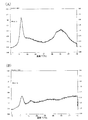
なお、酸化珪素は、水の分子が化学結合により吸着しやすいという特性を有している。よって、酸化珪素を含むCTOは、通常のCTOに比べてその表面に水分を吸着しやすいと考えられる。図3に、昇温脱離法(TDS:Thermal Desorption Spectroscopy)を用いて測定した、温度に対する基板からの脱ガスの量を示す。基板は、陽極を形成した後、正孔輸送性を有する層を形成する前の状態に相当する。 Silicon oxide has a characteristic that water molecules are easily adsorbed by chemical bonds. Therefore, it is considered that CTO containing silicon oxide is likely to adsorb moisture on the surface thereof as compared with normal CTO. FIG. 3 shows the amount of degassing from the substrate with respect to the temperature, measured using a temperature programmed desorption method (TDS: Thermal Desorption Spectroscopy). The substrate corresponds to a state after forming the anode and before forming a layer having a hole transporting property.
図3(A)は、陽極として酸化珪素とITOを用いたときの、温度に対する脱ガスの量を示している。図3(B)は、陽極としてITOを用いたときの、温度に対する脱ガスの量を示している。なお図3(A)と図3(B)は、共に陽極を形成した後、大気雰囲気下において200℃、1時間の加熱処理を施している。なお、図3(A)において用いた基板において、陽極の組成はO:Si:In:Sn=61:3:34:2である。 FIG. 3A shows the amount of degassing with respect to temperature when silicon oxide and ITO are used as the anode. FIG. 3B shows the amount of degassing with respect to temperature when ITO is used as the anode. In FIGS. 3A and 3B, after the anode is formed, heat treatment is performed at 200 ° C. for 1 hour in an air atmosphere. Note that in the substrate used in FIG. 3A, the composition of the anode is O: Si: In: Sn = 61: 3: 34: 2.
また図3において、横軸に示す温度はいずれも加熱処理の際に用いたヒーターの温度を示している。実際の基板の温度は、上記ヒーターの温度よりも低く、上記ヒーターの温度が高いほどその傾向が顕著である。 In FIG. 3, the temperature shown on the horizontal axis indicates the temperature of the heater used in the heat treatment. The actual temperature of the substrate is lower than the temperature of the heater, and the tendency is more remarkable as the temperature of the heater is higher.
図3(A)、図3(B)に示すように、いずれの基板も、横軸の温度が120℃程度(基板の温度もほぼ120℃程度)のところで、物理吸着した水の脱離を示すピークが観測されている点において共通している。しかし図3(A)に示すように、陽極として酸化珪素とITOを用いた場合、ITOのみを陽極として用いた場合とは異なり、横軸の温度が350℃〜370℃程度のところ(基板の温度が300℃〜320℃程度)で、再び水の脱離を示すピークが観測されている。350℃〜370℃において観測される上記ピークは、化学結合によって酸化珪素に吸着していた水分の脱離を示していると考えられる。 As shown in FIG. 3 (A) and FIG. 3 (B), the desorption of physically adsorbed water occurs when the temperature of the horizontal axis is about 120 ° C. (the temperature of the substrate is also about 120 ° C.). This is common in that the peak shown is observed. However, as shown in FIG. 3A, when silicon oxide and ITO are used as the anode, unlike the case where only ITO is used as the anode, the temperature on the horizontal axis is about 350 ° C. to 370 ° C. A peak indicating desorption of water is observed again at a temperature of about 300 ° C. to 320 ° C.). The peak observed at 350 ° C. to 370 ° C. is considered to indicate desorption of moisture adsorbed on silicon oxide by chemical bonding.
上述したTDSの測定結果から、酸化珪素を含むバリア層の表面には、CTOのみを用いた場合に比べて、水分が吸着しやすいことが分かる。陽極は表面が水分等で汚染されると仕事関数が小さくなるため、正孔の注入性が低下する。よって、注入バランスの悪下を引き起こしてしまい、結果的に内部量子効率が低減してしまう。また陽極の表面に吸着した水分によって、電界発光層の劣化が引き起こされる可能性がある。 From the above TDS measurement results, it can be seen that moisture is more easily adsorbed on the surface of the barrier layer containing silicon oxide than when only CTO is used. When the surface of the anode is contaminated with moisture or the like, the work function is reduced, so that the hole injectability is lowered. Therefore, the injection balance is deteriorated, and as a result, the internal quantum efficiency is reduced. In addition, the moisture adsorbed on the surface of the anode may cause deterioration of the electroluminescent layer.
そこで本発明では、バリア層を有する陽極を形成した後、正孔輸送性を有する層を形成する前に、該陽極に、大気雰囲気下で加熱処理または真空雰囲気下で加熱処理(真空ベーク)を施し、バリア層の表面に吸着した水分を除去することを特徴とする。上記構成により、バリア層に吸着した水分によりキャリアの注入バランスが悪化したり、信頼性が落ちたりするのを防ぐことができる。 Therefore, in the present invention, after forming an anode having a barrier layer and before forming a layer having hole transportability, the anode is subjected to heat treatment in an air atmosphere or heat treatment (vacuum bake) in a vacuum atmosphere. And removing moisture adsorbed on the surface of the barrier layer. With the above-described configuration, it is possible to prevent the carrier injection balance from being deteriorated or the reliability from being lowered due to moisture adsorbed on the barrier layer.
なお、本発明において電界発光層は複数の層で構成されており、これらの層は、キャリア輸送特性の観点から正孔注入層、正孔輸送層、発光層、電子輸送層、電子注入層などに分類することができる。正孔注入層と正孔輸送層との区別は必ずしも厳密なものではなく、これらは正孔輸送性(正孔移動度)が特に重要な特性である点において同じである。本明細書では便宜上正孔注入層は陽極に接する側の層であり、正孔注入層に接する層を正孔輸送層と呼んで区別する。電子輸送層、電子注入層についても同様であり、陰極に接する層を電子注入層と呼び、電子注入層に接する層を電子輸送層と呼んでいる。発光層は電子輸送層を兼ねる場合もあり、発光性電子輸送層とも呼ばれる。 In the present invention, the electroluminescent layer is composed of a plurality of layers, and these layers are a hole injection layer, a hole transport layer, a light emitting layer, an electron transport layer, an electron injection layer, etc. from the viewpoint of carrier transport properties. Can be classified. The distinction between a hole injection layer and a hole transport layer is not necessarily strict, and these are the same in that hole transportability (hole mobility) is a particularly important characteristic. In this specification, for convenience, the hole injection layer is a layer in contact with the anode, and the layer in contact with the hole injection layer is referred to as a hole transport layer to be distinguished. The same applies to the electron transport layer and the electron injection layer. The layer in contact with the cathode is called an electron injection layer, and the layer in contact with the electron injection layer is called an electron transport layer. The light emitting layer may also serve as an electron transport layer, and is also referred to as a light emitting electron transport layer.
また、電界発光層は有機材料のみならず、有機材料と無機材料とを複合化した材料、有機材料に金属錯体を添加した材料などを用いても、同様な機能が得られるのであれば、代用することができる。 In addition, the electroluminescent layer can be substituted if the same function can be obtained by using not only an organic material but also a material obtained by combining an organic material and an inorganic material, or a material obtained by adding a metal complex to an organic material. can do.
なおバリア層と透光性酸化物導電層との境界は、必ずしも明確である必要はない。例えば、陽極に含まれる珪素の濃度が、電界発光層に近いほど高くなるように、勾配を有して変化している場合も有り得る。この場合、バリア層と透光性酸化物導電層との境界は明確ではないが、電界発光層により近い領域がバリア層として機能することには、何ら変わりはない。 Note that the boundary between the barrier layer and the light-transmitting oxide conductive layer is not necessarily clear. For example, there may be a case where the concentration of silicon contained in the anode changes with a gradient so as to become higher as it is closer to the electroluminescent layer. In this case, the boundary between the barrier layer and the translucent oxide conductive layer is not clear, but there is no change in that the region closer to the electroluminescent layer functions as a barrier layer.
上記した本発明において、透光性酸化物導電層は、酸化インジウムスズ(ITO)、酸化亜鉛(ZnO)、酸化インジウム亜鉛(IZO)、ガリウムを添加した酸化亜鉛(GZO)などその他の透光性酸化物導電材料を用いることが可能である。好ましくは、陽極を、その透光性酸化物導電材料と酸化珪素を含むターゲットを用い、スパッタ法で形成されるものである。 In the above-described present invention, the light-transmitting oxide conductive layer includes other light-transmitting properties such as indium tin oxide (ITO), zinc oxide (ZnO), indium zinc oxide (IZO), and zinc oxide (GZO) to which gallium is added. An oxide conductive material can be used. Preferably, the anode is formed by a sputtering method using a target containing the light-transmitting oxide conductive material and silicon oxide.
本発明はバリア層を形成することで、正孔の注入性を向上させ、また正孔の移動度を高めることができるので、キャリアの注入バランスを高めることができ、結果的に内部量子効率を高めることができる。またバリア層に含まれる酸化珪素に吸着されている水分を、真空ベークにより除去してから正孔輸送性を有する層を形成するので、水分による注入性の低下や、電界発光層の劣化を防ぐことができる。従って、低消費電力で明るく、信頼性の高い発光素子を作製することができる。 In the present invention, by forming a barrier layer, the hole injection property can be improved and the hole mobility can be increased, so that the carrier injection balance can be increased, resulting in an increase in internal quantum efficiency. Can be increased. In addition, since the moisture adsorbed on the silicon oxide contained in the barrier layer is removed by vacuum baking, a layer having hole transportability is formed, thereby preventing deterioration of the injection property due to moisture and deterioration of the electroluminescent layer. be able to. Therefore, a light-emitting element with low power consumption and brightness and high reliability can be manufactured.
以下、本発明の実施の形態について説明する。本発明の発光素子は、透光性酸化物導電材料及び酸化珪素を用いて形成される陽極と、アルカリ金属又はアルカリ土類金属を含む陰極との間に、有機化合物を含む層が積層された電界発光層が、形成されている。有機化合物を含む層は、そのキャリア輸送特性から、正孔輸送層、発光層、電子輸送層に分類できる。また、陽極と正孔輸送層との間に正孔注入層を設けても良いし、陰極と電子輸送層との間に電子注入層を設けても良い。正孔注入層と正孔輸送層、及び電子注入層と電子輸送層の区別は必ずしも厳密なものではなく、これらは正孔輸送性(正孔移動度)及び電子輸送性(電子移動度)が特に重要(な特性)である点において同じである。また、電子輸送層と発光層の間に正孔ブロック層を設けた構成としても良い。発光層はホスト材料に顔料や金属錯体などのゲスト材料を添加して、発光色を異ならせても良い。すなわち、発光層は蛍光材料又は燐光材料を含ませて形成すれば良い。 Embodiments of the present invention will be described below. In the light-emitting element of the present invention, a layer containing an organic compound is stacked between an anode formed using a light-transmitting oxide conductive material and silicon oxide, and a cathode containing an alkali metal or an alkaline earth metal. An electroluminescent layer is formed. The layer containing an organic compound can be classified into a hole transport layer, a light emitting layer, and an electron transport layer from the carrier transport property. Further, a hole injection layer may be provided between the anode and the hole transport layer, or an electron injection layer may be provided between the cathode and the electron transport layer. The distinction between a hole injection layer and a hole transport layer, and an electron injection layer and an electron transport layer is not necessarily strict, and they have a hole transport property (hole mobility) and an electron transport property (electron mobility). It is the same in that it is particularly important (an important characteristic). Alternatively, a hole blocking layer may be provided between the electron transport layer and the light emitting layer. The light emitting layer may have a different emission color by adding a guest material such as a pigment or a metal complex to the host material. That is, the light emitting layer may be formed by including a fluorescent material or a phosphorescent material.
陽極は、酸化インジウムスズ(ITO)、酸化亜鉛(ZnO)、酸化インジウム亜鉛(IZO)、ガリウムを添加した酸化亜鉛(GZO)などから選ばれる透光性酸化物導電材料に酸化珪素を1〜10原子%含ませたものを用いる。そして、陽極の電界発光層と接する領域に、珪素の密度が陽極の他の領域よりも高く、絶縁性又は半絶縁性を有するバリア層を設ける。バリア層は、陽極から電界発光層へキャリアの移動が可能な程度の厚さ、すなわちトンネル電流により電流が流れる程度の厚さで形成する。そして該バリア層により、陽極の一部であり、なおかつバリア層と接している透光性酸化物導電層と、電界発光層とを物理的に隔てると共に、キャリアの移動を可能とすることができる。 As the anode, a light-transmitting oxide conductive material selected from indium tin oxide (ITO), zinc oxide (ZnO), indium zinc oxide (IZO), zinc oxide to which gallium is added (GZO), and the like is used. Use one containing atomic%. Then, a barrier layer having an insulating property or a semi-insulating property in which the silicon density is higher than the other regions of the anode is provided in a region of the anode in contact with the electroluminescent layer. The barrier layer is formed to a thickness that allows carriers to move from the anode to the electroluminescent layer, that is, a thickness that allows a current to flow due to a tunnel current. The barrier layer can physically separate the light-transmitting oxide conductive layer that is a part of the anode and is in contact with the barrier layer from the electroluminescent layer, and can move carriers. .
透光性酸化物導電材料を含む陽極は、当該透光性酸化物導電材料と酸化珪素を含むターゲットを用いたスパッタ法で形成することができる。ターゲットにおける、透光性酸化物導電材料に対する酸化珪素の含有率は、1乃至20重量%とすれば良く、好ましくは2乃至10重量%とする。酸化珪素の割合を高めると陽極の抵抗率が高くなるので、この範囲で適宜形成すれば良い。これにより、透光性酸化物導電材料と、1乃至10原子%、好ましくは2乃至5原子%の酸化珪素を含む陽極を得ることができる。勿論、同様な組成を得ることができれば、真空蒸着法で共蒸着して形成しても良い。なお、共蒸着とは同時に蒸発源を加熱し、成膜段階で異なる物質を混合する蒸着法をいう。 The anode including the light-transmitting oxide conductive material can be formed by a sputtering method using a target including the light-transmitting oxide conductive material and silicon oxide. The content of silicon oxide in the target with respect to the light-transmitting oxide conductive material may be 1 to 20% by weight, preferably 2 to 10% by weight. When the proportion of silicon oxide is increased, the resistivity of the anode is increased. Therefore, it may be appropriately formed within this range. Accordingly, an anode containing a light-transmitting oxide conductive material and 1 to 10 atomic percent, preferably 2 to 5 atomic percent of silicon oxide can be obtained. Of course, if a similar composition can be obtained, it may be formed by co-evaporation by a vacuum deposition method. Note that co-evaporation is an evaporation method in which an evaporation source is heated at the same time and different substances are mixed in a film formation stage.
バリア層は、酸化珪素及び透光性酸化物導電材料を含む陽極の表面から、該透光性酸化物導電材料を選択的に除去して、添加されている珪素の密度を高めることで形成することができる。例えば、透光性酸化物導電材料を選択的に除去することが可能な溶液で、表面を処理する方法、水素、酸素、フッ素から選ばれた一種又は複数種の気体を用いたプラズマ処理、窒素、アルゴンなどの不活性気体を用いたプラズマ処理などにより、当該バリア層を形成することができる。 The barrier layer is formed by selectively removing the light-transmitting oxide conductive material from the surface of the anode containing silicon oxide and the light-transmitting oxide conductive material and increasing the density of the added silicon. be able to. For example, a method of treating a surface with a solution capable of selectively removing a light-transmitting oxide conductive material, plasma treatment using one or more kinds of gases selected from hydrogen, oxygen, and fluorine, nitrogen The barrier layer can be formed by plasma treatment using an inert gas such as argon.
陽極の表面から透光性酸化物導電材料を選択的に除去することでバリア層を形成する場合、当該バリア層は、透光性酸化物導電層を緻密に作ると形成されにくく、ある程度サブミクロンレベルで粗く作ることが好ましい。上記構成により、該透光性酸化物導電材料を選択的に除去する際に、添加されている珪素の密度を透光性酸化物導電材料に対して、効率的に高めることができる。 In the case of forming a barrier layer by selectively removing the light-transmitting oxide conductive material from the surface of the anode, the barrier layer is difficult to be formed when the light-transmitting oxide conductive layer is densely formed. It is preferable to make it roughly at a level. With the above structure, when the light-transmitting oxide conductive material is selectively removed, the density of added silicon can be efficiently increased with respect to the light-transmitting oxide conductive material.
またバリア層は、透光性酸化物導電層を形成する際に、意図的に表面に近い領域における(酸化)珪素の密度を高めることで、形成しても良い。具体的には、透光性酸化物導電層を形成した後、(酸化)珪素の密度が高くなるようにスパッタのターゲットの組成を変更するなどして、(酸化)珪素の重量%がより高いバリア層を、先に形成された透光性酸化物導電層上に新たに形成しても良い。 The barrier layer may be formed by intentionally increasing the density of (oxide) silicon in a region close to the surface when forming the translucent oxide conductive layer. Specifically, after the formation of the light-transmitting oxide conductive layer, the composition of the sputtering target is changed so that the density of (oxide) silicon is increased, so that the weight percent of (oxide) silicon is higher. A barrier layer may be newly formed on the previously formed translucent oxide conductive layer.
そして本発明では、電界発光層を形成する前に、大気雰囲気下または真空雰囲気下(好ましくは10-4〜10-8Pa程度)において、基板の温度を200℃〜450℃、好ましくは250℃〜300℃とし、陽極に加熱処理を施す。また清浄化し平坦性を高めるために拭浄処理や研磨処理を行っても良い。 In the present invention, before forming the electroluminescent layer, the temperature of the substrate is 200 ° C. to 450 ° C., preferably 250 ° C. in an air atmosphere or a vacuum atmosphere (preferably about 10 −4 to 10 −8 Pa). ˜300 ° C., and heat treatment is performed on the anode. Moreover, in order to clean and improve flatness, you may perform a wiping process and a grinding | polishing process.
上記の構成を有する発光素子は、陽極と正孔注入層または正孔輸送層とが物理的に隔てられているので、陽極がもつ本来の仕事関数の効果が得られる。すなわち、正孔注入層に対する正孔注入効率を高めることができ、注入バランスが高められるため、結果的に内部量子効率を高めることができる。 In the light-emitting element having the above structure, since the anode and the hole injection layer or the hole transport layer are physically separated, the effect of the original work function of the anode can be obtained. That is, the hole injection efficiency with respect to the hole injection layer can be increased and the injection balance can be increased. As a result, the internal quantum efficiency can be increased.
図4(A)に、本発明によって得られる発光素子の構成を示す。図4(A)に示す発光素子は、基板100上に、陽極101と、陽極101上に形成された電界発光層102と、電界発光層102上に形成された陰極103とを有している。
FIG. 4A shows a structure of a light-emitting element obtained by the present invention. A light-emitting element illustrated in FIG. 4A includes an
陽極101は、バリア層109aと、透光性酸化物導電層109bとを有しており、該バリア層109aによって、透光性酸化物導電層109bと電界発光層102とが物理的に隔てられている。
The
陰極103は、一般的に発光素子の陰極に用いられるような仕事関数の小さい金属、合金、電気伝導性化合物、およびこれらの混合物などを用いることができる。具体的には、LiやCs等のアルカリ金属、およびMg、Ca、Sr等のアルカリ土類金属、およびこれらを含む合金(Mg:Ag、Al:Liなど)の他、YbやEr等の希土類金属を用いて形成することもできる。また、電子注入性の高い材料を含む層を陰極103に接するように形成することで、アルミニウム、透光性酸化物導電材料等を用いた、通常の導電膜も用いることができる。
As the
また図4(A)では、電界発光層102は、第1〜第5の層104〜108を有している。
In FIG. 4A, the
バリア層109a上に形成されている第1の層104は、正孔注入層として機能するため、正孔輸送性を有し、なおかつイオン化ポテンシャルが比較的小さく、正孔注入性が高い材料を用いるのが望ましい。大別すると金属酸化物、低分子系有機化合物、および高分子系有機化合物に分けられる。金属酸化物であれば、例えば、酸化バナジウム、酸化モリブデン、酸化ルテニウム、酸化アルミニウムなど用いることができる。低分子系有機化合物あれば、例えば、m−MTDATAに代表されるスターバースト型アミン、銅フタロシアニン(略称:Cu−Pc)に代表される金属フタロシアニン、フタロシアニン(略称:H2−Pc)、2,3−ジオキシエチレンチオフェン誘導体などを用いることができる。低分子系有機化合物と上記金属酸化物とを共蒸着させた膜であっても良い。高分子系有機化合物であれば、例えば、ポリアニリン(略称:PAni)、ポリビニルカルバゾール(略称:PVK)、ポリチオフェン誘導体などの高分子を用いることができる。ポリチオフェン誘導体の一つであるポリエチレンジオキシチオフェン(略称:PEDOT)にポリスチレンスルホン酸(略称:PSS)をドープしたものを用いても良い。また、ベンゾオキサゾール誘導体と、TCQn、FeCl3、C60またはF4TCNQのいずれか一または複数の材料とを併せて用いても良い。
Since the
第1の層104上に形成されている第2の層105は、正孔輸送層として機能するため、正孔輸送性が高く、結晶性の低い公知の材料を用いることが望ましい。具体的には芳香族アミン系(すなわち、ベンゼン環−窒素の結合を有するもの)の化合物が好適であり、例えば、4,4−ビス[N−(3−メチルフェニル)−N−フェニルアミノ]ビフェニル(TPD)や、その誘導体である4,4’−ビス[N−(1−ナフチル)−N−フェニル−アミノ]ビフェニル(α−NPD)などがある。4,4’,4’’−トリス(N,N−ジフェニルアミノ)トリフェニルアミン(TDATA)や、MTDATAなどのスターバースト型芳香族アミン化合物も用いることができる。また4,4’,4’’−トリス(N−カルバゾリル)トリフェニルアミン(略称:TCTA)を用いても良い。また高分子材料としては、良好な正孔輸送性を示すポリ(ビニルカルバゾール)などを用いることができる。
Since the
第2の層105上に形成されている第3の層106は、発光層として機能するため、イオン化ポテンシャルが大きく、かつバンドギャップの大きな材料を用いるのが望ましい。具体的には、例えば、トリス(8−キノリノラト)アルミニウム(Alq3)、トリス(4−メチル−8−キノリノラト)アルミニウム(Almq3)、ビス(10−ヒドロキシベンゾ[η]−キノリナト)ベリリウム(BeBq2)、ビス(2−メチル−8−キノリノラト)−(4−ヒドロキシ−ビフェニリル)−アルミニウム(BAlq)、ビス[2−(2−ヒドロキシフェニル)−ベンゾオキサゾラト]亜鉛(Zn(BOX)2)、ビス[2−(2−ヒドロキシフェニル)−ベンゾチアゾラト]亜鉛(Zn(BTZ)2)などの金属錯体を用いることができる。また、各種蛍光色素(クマリン誘導体、キナクリドン誘導体、ルブレン、4,4−ジシアノメチレン、1−ピロン誘導体、スチルベン誘導体、各種縮合芳香族化合物など)も用いることができる。白金オクタエチルポルフィリン錯体、トリス(フェニルピリジン)イリジウム錯体、トリス(ベンジリデンアセトナート)フェナントレンユーロピウム錯体などの燐光材料も用いることができる。
Since the
また、第3の層106に用いるホスト材料としては、上述した例に代表されるホール輸送材料や電子輸送材料を用いることができる。また、4,4’−N,N’−ジカルバゾリルビフェニル(略称:CBP)などのバイポーラ性の材料も用いることができる。
As the host material used for the
第3の層106上に形成されている第4の層107は、電子輸送層として機能するため、電子輸送性の高い材料を用いることが望ましい。具体的には、Alq3に代表されるような、キノリン骨格またはベンゾキノリン骨格を有する金属錯体やその混合配位子錯体などを用いることができる。具体的には、Alq3、Almq3、BeBq2、BAlq、Zn(BOX)2、Zn(BTZ)2などの金属錯体が挙げられる。さらに、金属錯体以外にも、2−(4−ビフェニリル)−5−(4−tert−ブチルフェニル)−1,3,4−オキサジアゾール(PBD)、1,3−ビス[5−(p−tert−ブチルフェニル)−1,3,4−オキサジアゾール−2−イル]ベンゼン(OXD−7)などのオキサジアゾール誘導体、3−(4−tert−ブチルフェニル)−4−フェニル−5−(4−ビフェニリル)−1,2,4−トリアゾール(TAZ)、3−(4−tert−ブチルフェニル)−4−(4−エチルフェニル)−5−(4−ビフェニリル)−1,2,4−トリアゾール(p−EtTAZ)などのトリアゾール誘導体、TPBIのようなイミダゾール誘導体、バソフェナントロリン(BPhen)、バソキュプロイン(BCP)などのフェナントロリン誘導体を用いることができる。
Since the
第4の層107上に形成されている第5の層108は、電子注入層として機能するため、電子注入性の高い材料を用いるのが望ましい。具体的には、LiF、CsFなどのアルカリ金属ハロゲン化物や、CaF2のようなアルカリ土類ハロゲン化物、Li2Oなどのアルカリ金属酸化物のような絶縁体の超薄膜がよく用いられる。また、リチウムアセチルアセトネート(略称:Li(acac)や8−キノリノラト−リチウム(略称:Liq)などのアルカリ金属錯体も有効である。また、モリブデン酸化物(MoOx)やバナジウム酸化物(VOx)、ルテニウム酸化物(RuOx)、タングステン酸化物(WOx)等の金属酸化物またはベンゾオキサゾール誘導体と、アルカリ金属、アルカリ土類金属、または遷移金属のいずれか一または複数の材料とを含むようにしても良い。
Since the
上記構成を有する発光素子において、陽極101と陰極103の間に電圧を印加し、電界発光層102に順方向バイアスの電流を供給することで、第3の層106から光が発生し、該光を陽極101側から取り出すことができる。なお、電界発光層102は、必ずしもこれら第1〜第5の層を全て有している必要はない。本発明では、少なくとも電子輸送層または電子注入層のいずれか一方と、発光層とを有していれば良い。また必ずしも第3の層106からのみ発光が得られるわけではなく、第1〜第5の層に用いられる材料の組み合わせによっては、第3の層106以外の層から発光が得られる場合もある。
In the light-emitting element having the above structure, light is generated from the
なお色によっては、燐光材料の方が蛍光材料よりも、駆動電圧を低くすることができ、信頼性も高い場合がある。そこで、三原色の各色に対応する発光素子を用いて、フルカラーの表示を行なう場合は、蛍光材料を用いた発光素子と、燐光材料を用いた発光素子とを組み合わせて、各色の発光素子における劣化の度合いを揃えるようにしても良い。 Note that depending on the color, the phosphorescent material can have a lower driving voltage and higher reliability than the fluorescent material. Therefore, when full-color display is performed using light-emitting elements corresponding to the three primary colors, a combination of a light-emitting element using a fluorescent material and a light-emitting element using a phosphorescent material can reduce the deterioration of the light-emitting element of each color. You may make it arrange | equalize a degree.
次に陰極側から光を取り出すことができる、発光素子の構成について説明する。図4(B)に、本発明によって得られる発光素子の構成を示す。図4(B)に示す発光素子は、基板110上に、陽極111と、陽極111上に形成された電界発光層112と、電界発光層112上に形成された陰極113とを有している。
Next, a structure of a light-emitting element that can extract light from the cathode side will be described. FIG. 4B shows a structure of a light-emitting element obtained by the present invention. A light-emitting element illustrated in FIG. 4B includes an
陽極111として、例えばTiN、ZrN、Ti、W、Ni、Pt、Cr、Ag等の1つまたは複数からなる単層膜の他、窒化チタン膜とアルミニウムを主成分とする膜との積層、窒化チタン膜とアルミニウムを主成分とする膜と窒化チタン膜との三層構造等を用いることができる。また、上記光を反射することができる材料の上に、ITO、酸化珪素を含む酸化インジウムスズ(以下、ITSOとする)、IZOなどを用いた透光性酸化物導電層と、バリア層とを積層し、陽極111として用いてもよい。図4(B)では、基板110に近い方から、Al−Si層114、Ti層115、透光性酸化物導電層116と、バリア層117とを積層することにより、陽極111が形成されている。
As the
透光性酸化物導電層116は、透光性酸化物導電材料及び酸化珪素を用いて形成されている。そしてバリア層117は、酸化珪素、または透光性酸化物導電材料及び酸化珪素を用いて形成されている。(酸化)珪素の密度は、透光性酸化物導電層116よりもバリア層117の方が高い。
The light-transmitting oxide
また陰極103は、透光性を有している。具体的には、酸化インジウムスズ(ITO)、酸化亜鉛(ZnO)、酸化インジウム亜鉛(IZO)、ガリウムを添加した酸化亜鉛(GZO)などから選ばれる透光性酸化物導電材料を用いていても良いし、該透光性酸化物導電材料と共に酸化珪素を用いても良い。この場合、電界発光層112に、陰極103に接するように電子注入層を設けるのが望ましい。
Moreover, the
また、仕事関数の小さい金属、合金、電気伝導性化合物、およびこれらの混合物などを、光が透過する程度の膜厚で形成し、陰極103として用いることができる。具体的には、LiやCs等のアルカリ金属、およびMg、Ca、Sr等のアルカリ土類金属、およびこれらを含む合金(Mg:Ag、Al:Liなど)の他、YbやEr等の希土類金属を用い、5nm〜30nm程度の膜厚で陰極103を形成することができる。また電子注入層を設ける場合、Alなどの他の導電層を、光が透過する程度の膜厚で形成し、陰極103として用いることも可能である。なお、光が透過する程度の膜厚で陰極103を形成する場合、該陰極上に透光性酸化物導電材料を用いて透光性を有する導電層を形成し、陰極のシート抵抗を抑えるようにしても良い。
Further, a metal, an alloy, an electrically conductive compound, a mixture thereof, or the like having a low work function can be formed to have a thickness enough to transmit light and used as the
電界発光層112は、図4(A)に示した電界発光層102と同じ構造を有していてもよい。ただし、陰極に用いられる材料の仕事関数が十分小さくない場合、電子注入層を設けることが望ましい。
The
次に、本発明の発光装置の具体的な作製方法について説明する。なお本実施の形態では、nチャネル型TFTと、pチャネル型TFTとを同一基板上に作製する場合を例に挙げて説明する。 Next, a specific method for manufacturing the light-emitting device of the present invention will be described. Note that in this embodiment, an example in which an n-channel TFT and a p-channel TFT are formed over the same substrate will be described.
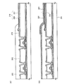
まず図5(A)に示すように、基板201上に下地膜202を成膜する。基板201には、例えばバリウムホウケイ酸ガラスや、アルミノホウケイ酸ガラスなどのガラス基板、石英基板、セラミック基板等を用いることができる。また、ステンレス基板を含む金属基板またはシリコン基板の表面に絶縁膜を形成したものを用いても良い。プラスチック等の可撓性を有する合成樹脂からなる基板は、一般的に上記基板と比較して耐熱温度が低い傾向にあるが、作製工程における処理温度に耐え得るのであれば用いることが可能である。
First, as shown in FIG. 5A, a
下地膜202は基板201中に含まれるNaなどのアルカリ金属やアルカリ土類金属が、半導体膜中に拡散し、TFTなどの半導体素子の特性に悪影響を及ぼすのを防ぐために設ける。よってアルカリ金属やアルカリ土類金属の半導体膜への拡散を抑えることができる酸化珪素や、窒化珪素、窒化酸化珪素などの絶縁膜を用いて形成する。本実施の形態では、プラズマCVD法を用いて窒化酸化珪素膜を10〜400nm(好ましくは50〜300nm)の膜厚になるように成膜した。
The
なお下地膜202は単層であっても複数の絶縁膜を積層したものであっても良い。またガラス基板、ステンレス基板またはプラスチック基板のように、アルカリ金属やアルカリ土類金属が多少なりとも含まれている基板を用いる場合、不純物の拡散を防ぐという観点から下地膜を設けることは有効であるが、石英基板など不純物の拡散がさして問題とならない場合は、必ずしも設ける必要はない。
Note that the
次に下地膜202上に、活性層として用いる島状の半導体膜203、204を形成する。島状の半導体膜203、204の膜厚は25〜100nm(好ましくは30〜60nm)とする。なお島状の半導体膜203、204は、非晶質半導体であっても良いし、セミアモルファス半導体(微結晶半導体)または多結晶半導体であっても良い。また半導体は珪素だけではなくシリコンゲルマニウムも用いることができる。シリコンゲルマニウムを用いる場合、ゲルマニウムの濃度は0.01〜4.5atomic%程度であることが好ましい。
Next, island-shaped
多結晶半導体を用いる場合、まず非晶質半導体を成膜して、公知の結晶化方法を用いて該非晶質半導体を結晶化すれば良い。公知の結晶化方法としては、加熱器による加熱で結晶化を行なう方法、レーザー光の照射で結晶化を行なう方法、触媒金属を用いて結晶化を行なう方法、赤外光を用いて結晶化を行なう方法等が挙げられる。 In the case of using a polycrystalline semiconductor, an amorphous semiconductor is first formed, and the amorphous semiconductor may be crystallized using a known crystallization method. Known crystallization methods include crystallization by heating with a heater, crystallization by laser light irradiation, crystallization using a catalytic metal, and crystallization using infrared light. The method of performing etc. are mentioned.
例えばレーザー光を用いて結晶化する場合、パルス発振型または連続発振型のエキシマレーザー、YAGレーザー、YVO4レーザー等を用いれば良い。例えばYAGレーザーを用いる場合は、半導体膜に吸収されやすい第2高調波の波長を用いるのが望ましい。そして発振周波数30〜300kHz、エネルギー密度を300〜600mJ/cm2(代表的には350〜500mJ/cm2)とし、任意のポイントに数ショットずつ照射できるように走査速度を設定すると良い。 For example, when crystallization is performed using laser light, a pulsed or continuous wave excimer laser, YAG laser, YVO 4 laser, or the like may be used. For example, when a YAG laser is used, it is desirable to use a second harmonic wavelength that is easily absorbed by the semiconductor film. The oscillation frequency 30~300KHz, the energy density was 300~600mJ / cm 2 (typically 350~500mJ / cm 2), it may be set the scanning speed to be irradiated by several shots to any point.
次に、該島状の半導体膜203、204を用いてTFTを形成する。なお本実施の形態では、図5(B)に示すように、島状の半導体膜203、204を用いてトップゲート型のTFT205、206を形成するが、TFTはトップゲート型に限定されず、例えばボトムゲート型であっても良い。
Next, a TFT is formed using the island-shaped
具体的には、島状の半導体膜203、204を覆うようにゲート絶縁膜207を成膜する。そして、ゲート絶縁膜207上に導電膜を成膜し、パターニングすることで、ゲート電極208、209を形成する。そして、ゲート電極208、209や、あるいはレジストを成膜しパターニングしたものをマスクとして用い、島状の半導体膜203、204にn型またはp型を付与する不純物を添加し、ソース領域、ドレイン領域、さらにはLDD領域等を形成する。なおここでは、TFT205をn型、TFT206をp型とする。
Specifically, a
なおゲート絶縁膜207には、例えば酸化珪素、窒化珪素または窒化酸化珪素等を用いることができる。また成膜方法は、プラズマCVD法、スパッタ法などを用いることができる。例えば、酸化珪素を用いたゲート絶縁膜をプラズマCVD法で成膜する場合、TEOS(Tetraethyl Orthosilicate)とO2を混合したガスを用い、反応圧力40Pa、基板温度300〜400℃、高周波(13.56MHz)電力密度0.5〜0.8W/cm2とし、成膜する。
Note that for the
また窒化アルミニウムをゲート絶縁膜207として用いることができる。窒化アルミニウムは熱伝導率が比較的高く、TFTで発生した熱を効率的に発散させることができる。またアルミニウムの含まれない酸化珪素や酸化窒化珪素等を形成した後、窒化アルミニウムを積層したものをゲート絶縁膜として用いても良い。
Aluminum nitride can be used for the
上記一連の工程によって、nチャネル型TFT205と、発光素子に供給する電流を制御するpチャネル型TFT206とを形成することができる。なおTFTの作製方法は、上述した工程に限定されない。液滴吐出法によりゲート電極や配線を作製しても良い。
Through the above series of steps, an n-
次に、TFT205、206を覆うように、パッシベーション膜210を成膜する。パッシベーション膜210は、珪素を含む酸化珪素、窒化珪素、酸化窒化珪素などの絶縁膜を用いることができ、その厚さは100〜200nm程度とする。
Next, a
次に、島状の半導体膜203、204に添加された不純物元素を活性化するために、熱処理を行なう。この工程はファーネスアニール炉を用いる熱アニール法、レーザーアニール法、またはラピッドサーマルアニール法(RTA法)を用いることができる。例えば熱アニール法で活性化を行なう場合、酸素濃度が1ppm以下、好ましくは0.1ppm以下の窒素雰囲気中で、400〜700℃(好ましくは500〜600℃)で行なう。さらに、3〜100%の水素を含む雰囲気中で、300〜450℃で1〜12時間の熱処理を行い、島状の半導体膜を水素化する工程を行なう。この工程は、熱的に励起された水素によりダングリングボンドを終端する目的で行なわれる。水素化の他の手段として、プラズマ水素化(プラズマにより励起された水素を用いる)を行っても良い。また活性化処理はパッシベーション膜210を成膜する前に行っても良い。
Next, heat treatment is performed to activate the impurity element added to the island-shaped
次に図5(C)に示すように、パッシベーション膜210を覆うように、第1の層間絶縁膜211と第2の層間絶縁膜212を成膜する。第1の層間絶縁膜211として、有機樹脂膜、無機絶縁膜、シロキサン系材料を出発材料として形成されたSi−O結合とSi−CHX結合手を含む絶縁膜等を用いることができる。本実施の形態では、シロキサン系材料を用いて形成された絶縁膜を用いる。第2の層間絶縁膜212は、水分や酸素などの発光素子の劣化を促進させる原因となる物質を、他の絶縁膜と比較して透過させにくい膜を用いる。代表的には、RFスパッタ法で形成された窒化珪素膜を用いるが、その他にもダイヤモンドライクカーボン(DLC)膜や、窒化アルミニウム膜などを用いることができる。
Next, as shown in FIG. 5C, a first
次いで、パッシベーション膜210、第1の層間絶縁膜211及び第2の層間絶縁膜212をエッチングし、コンタクトホールを形成する。そして、島状の半導体膜203、204と接続する配線213〜216を形成する。
Next, the
次に、第2の層間絶縁膜212及び配線213〜216を覆って透光性酸化物導電層217を形成する。本実施の形態では、スパッタ法を用い、ITSOで透光性酸化物導電層217を形成した。なおITSOの他、酸化珪素を含んだ酸化インジウムに、さらに2〜20%の酸化亜鉛(ZnO)を混合し、透光性酸化物導電層217として用いても良い。
Next, a light-transmitting oxide
ITSOを用いる場合、ターゲットとしてITOに酸化珪素が2〜10重量%含まれたものを用いることができる。具体的に本実施の形態では、In2O3と、SnO2と、SiO2とが85:10:5の重量%の割合で含むターゲットを用い、Arの流量を50sccm、O2の流量を3sccm、スパッタ圧力を0.4Pa、スパッタ電力を1kW、成膜速度30nm/minとし、105nmの膜厚で、透光性酸化物導電層217を形成した。
When ITSO is used, an ITO containing 2 to 10% by weight of silicon oxide can be used as a target. Specifically, in this embodiment, a target containing In 2 O 3 , SnO 2 , and SiO 2 at a ratio of 85: 10: 5 wt% is used, the flow rate of Ar is 50 sccm, and the flow rate of O 2 is The light-transmitting oxide
そして本実施の形態では、透光性酸化物導電層217上に透光性酸化物導電層217よりもSi(O2)の密度が高いバリア層218を形成する。具体的に本実施の形態では、In2O3と、SnO2と、SiO2とが83:7:10の重量%の割合で含むターゲットを用い、スパッタ法で、バリア層218を5nmの膜厚になるように形成する。
In this embodiment, the
なお、バリア層218を形成する前に、透光性酸化物導電層217の表面が平坦化されるように、CMP法、ポリビニルアルコール系の多孔質体による拭浄などで、その表面を研磨しておいても良い。
Before forming the
また、透光性酸化物導電層の表面から透光性酸化物導電材料を選択的に除去して、添加されている(酸化)珪素の密度を高めることで、バリア層を形成するようにしても良い。この場合バリア層は、透光性酸化物導電層をパターニングした後で形成しても良いし、或いは、隔壁を形成した後で形成しても良い。 In addition, by selectively removing the light-transmitting oxide conductive material from the surface of the light-transmitting oxide conductive layer and increasing the density of the added (oxide) silicon, the barrier layer is formed. Also good. In this case, the barrier layer may be formed after the light-transmitting oxide conductive layer is patterned, or may be formed after the partition walls are formed.
次に、図6(A)に示すように、透光性酸化物導電層217及びバリア層218をパターニングすることで、配線216に接続された陽極219を形成する。なお、220はパターニング後の透光性酸化物導電層、221はパターニング後のバリア層に相当する。
Next, as illustrated in FIG. 6A, the light-transmitting oxide
そして隔壁222を、第2の層間絶縁膜212上に形成する。隔壁222として、有機樹脂膜、無機絶縁膜、シロキサン系材料を出発材料として形成されたSi−O結合とSi−CHX結合手を含む絶縁膜等を用いることができる。隔壁222は、陽極219の端部を覆い、なおかつ陽極219と重なる領域において開口部を有するようにする。隔壁222の開口部における端部は、該端部において後に成膜される電界発光層に穴があかないように、丸みを帯びさせることが望ましい。具体的には、開口部における隔壁222の断面が描いている曲線の曲率半径が、0.2〜2μm程度であることが望ましい。
A
図6(A)では、隔壁222として、ポジ型の感光性のアクリル樹脂を用いた例を示している。感光性の有機樹脂には、光、電子、イオンなどのエネルギー線が露光された箇所が除去されるポジ型と、露光された箇所が残るネガ型とがある。本発明ではネガ型の有機樹脂(膜)を用いても良い。また感光性のポリイミドを用いて隔壁222を形成しても良い。ネガ型のアクリルを用いて隔壁222を形成した場合、開口部における端部が、S字状の断面形状となる。このとき開口部の上端部及び下端部における曲率半径は、0.2〜2μmとすることが望ましい。
FIG. 6A illustrates an example in which a positive photosensitive acrylic resin is used for the
上記構成により、後に形成される電界発光層や陰極のカバレッジを良好とすることができ、陽極219と陰極が電界発光層に形成された穴においてショートするのを防ぐことができる。また電界発光層の応力を緩和させることで、発光領域が減少するシュリンクとよばれる不良を低減させることができ、信頼性を高めることができる。
With the above structure, coverage of an electroluminescent layer and a cathode to be formed later can be improved, and a short circuit between the
次に本発明では、電界発光層を成膜する前に、隔壁222及び陽極219に吸着した水分や酸素等を除去するために、大気雰囲気下で加熱処理または真空雰囲気下で加熱処理(真空ベーク)を行なう。具体的には、基板の温度を200℃〜450℃、好ましくは250〜300℃で、0.5〜20時間程度、真空雰囲気下で加熱処理を行なう。望ましくは3×10⁻⁷Torr以下とし、可能であるならば3×10⁻⁸Torr以下とするのが最も望ましい。そして、真空雰囲気下で加熱処理を行なった後に電界発光層を成膜する場合、電界発光層を成膜する直前まで当該基板を真空雰囲気下に置いておくことで、信頼性をより高めることができる。また真空ベークの前または後に、陽極219に紫外線を照射してもよい。
Next, in the present invention, before the electroluminescent layer is formed, in order to remove moisture, oxygen, and the like adsorbed on the
次に図6(B)に示すように、陽極219上に電界発光層223を成膜する。電界発光層223は、単数または複数の層からなり、各層には有機材料のみならず無機材料が含まれていても良い。電界発光層223の具体的な構成については、図4についての上記説明を参照することができる。次に、電界発光層223を覆うように陰極224を形成する。陽極219、電界発光層223、陰極224は、隔壁222の開口部において重なり合っており、該重なり合っている部分が発光素子225に相当する。
Next, as illustrated in FIG. 6B, an
なお発光素子225を形成したら、陰極224上に、保護膜を形成しても良い。保護膜は第2の層間絶縁膜212と同様に、水分や酸素などの発光素子の劣化を促進させる原因となる物質を、他の絶縁膜と比較して透過させにくい膜を用いる。代表的には、例えばDLC膜、窒化炭素膜、RFスパッタ法で形成された窒化珪素膜等を用いるのが望ましい。また上述した水分や酸素などの物質を透過させにくい膜と、該膜に比べて水分や酸素などの物質を透過させやすい膜とを積層させて、保護膜として用いることも可能である。
Note that after the light-emitting
なお図6(B)では、発光素子から発せられる光が基板201側に照射される構成を示しているが、光が基板とは反対側に向かうような構造の発光素子としても良い。
Note that FIG. 6B illustrates a structure in which light emitted from the light-emitting element is emitted to the
なお、実際には図6(B)まで完成したら、さらに外気に曝されないように気密性が高く、脱ガスの少ない保護フィルム(ラミネートフィルム、紫外線硬化樹脂フィルム等)や透光性のカバー材でパッケージング(封入)することが好ましい。その際、カバー材の内部を不活性雰囲気にしたり、内部に吸湿性材料(例えば酸化バリウム)を配置したりすると発光素子の信頼性が向上する。 Actually, when completed up to FIG. 6B, a protective film (laminate film, ultraviolet curable resin film, etc.) or a translucent cover material with high air tightness and low outgassing so as not to be exposed to the outside air. It is preferable to package (enclose). At that time, if the inside of the cover material is made an inert atmosphere or a hygroscopic material (for example, barium oxide) is arranged inside, the reliability of the light emitting element is improved.
なお本発明の発光装置の作製方法は、必ずしも上述した形態に限定されない。上述した作製方法は本発明の一形態について具体的に説明しただけであり、本発明は、上述した形態に限定されるものではなく、発明の技術的範囲を超えない各種の変形が可能である。 Note that the method for manufacturing a light-emitting device of the present invention is not necessarily limited to the above-described embodiment. The manufacturing method described above is only a specific description of one embodiment of the present invention, and the present invention is not limited to the above-described embodiment, and various modifications that do not exceed the technical scope of the invention are possible. .
本実施例では、本発明の作製方法によって得られる発光装置の、画素の一形態について説明する。 In this example, one mode of a pixel of a light-emitting device obtained by a manufacturing method of the present invention will be described.
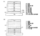
図8に、本実施例の発光装置の断面図を示す。図8では、基板7000上に、トランジスタ7001〜7003が形成されている。トランジスタ7001〜7003は第1の層間絶縁膜7004で覆われており、第1の層間絶縁膜7004上には、コンタクトホールを介してトランジスタ7001〜7003と接続されている配線7005〜7007が形成されている。
FIG. 8 shows a cross-sectional view of the light emitting device of this example. In FIG. 8,
そして配線7005〜7007を覆うように、第1の層間絶縁膜7004上に、第2の層間絶縁膜7008と第3の層間絶縁膜7009とが積層されている。なお、第1の層間絶縁膜7004と第2の層間絶縁膜7008は、有機樹脂膜、無機絶縁膜、シロキサン系材料を出発材料として形成されたSi−O結合とSi−CHX結合手を含む絶縁膜等を用いることができる。本実施例では非感光性のアクリルを用いる。第3の層間絶縁膜7009は、水分や酸素などの発光素子の劣化を促進させる原因となる物質を、他の絶縁膜と比較して透過させにくい膜を用いる。代表的には、例えばDLC膜、窒化炭素膜、RFスパッタ法で形成された窒化珪素膜等を用いるのが望ましい。
A second
第3の層間絶縁膜7009上には、コンタクトホールを介して配線7005〜7007に電気的に接続された、配線7010〜7012が形成されている。また配線7010〜7012は、光が透過しないような材料を用いる。そして、配線7010〜7012上には、透光性酸化物導電層7013〜7015と、バリア層7016〜7018とが積層されている。配線7010〜7012の一部と、透光性酸化物導電層7013〜7015と、バリア層7016〜7018とによって陽極7019〜7021が形成されている。
Over the third
なお図8では、陽極7019〜7021とTFTに直接接続されている配線7010〜7012とが異なる層に形成されているので、陽極7019〜7021のレイアウトの面積を広げることができ、よって、発光素子として光が得られる領域を広げることができる。
In FIG. 8, since the
また第3の層間絶縁膜7009上には、シロキサン系材料を出発材料として形成されたSi−O結合とSi−CHX結合手を含む絶縁膜や、有機樹脂膜、無機絶縁膜など、を用いて形成された隔壁7040が形成されている。隔壁7040は開口部を有しており、該開口部において、陽極7019〜7021と、電界発光層7022〜7024と、陰極7025とが重なり合うことで、発光素子7026〜7028が形成されている。電界発光層7022〜7024は、複数の層が積層された構成を有している。陰極7025は、光を透過するような材料もしくは膜厚で形成する。なお、隔壁7040及び陰極7025上に、保護膜を成膜しても良い。
In addition, an insulating film including a Si—O bond and a Si—CH X bond formed using a siloxane-based material as a starting material, an organic resin film, an inorganic insulating film, or the like is used over the third
7030は、発光素子7026〜7028を封止するためのカバー材であり、透光性を有している。カバー材7030には、可視光を遮蔽するための遮蔽膜7031と、各色の画素に対応した着色層7032〜7034とを有するカラーフィルター7035が形成されている。図8では、着色層7032において、発光素子7026から発せられる光のうち、赤色の波長領域の光が選択的に透過される。また着色層7033において、発光素子7027から発せられる光のうち、緑色の波長領域の光が選択的に透過される。また着色層7034において、発光素子7028から発せられる光のうち、青色の波長領域の光が選択的に透過される。
7030 is a cover material for sealing the
なお図8では、遮蔽膜7031に、黒色の顔料と乾燥剤とを樹脂に分散させて形成する。上記構成により、発光素子の劣化を防ぐことができる。
In FIG. 8, a black pigment and a desiccant are dispersed in the
遮蔽膜7031は、発光素子7026〜7028どうしの間と重なるようにレイアウトされており、遮蔽膜7031により、発光素子の光が、隣接する画素に対応する着色層を透過してしまうのを防ぐことができる。
The
なお図8では、各色に対応する画素ごとに、含まれる電界発光材料または素子構成が異なる電界発光層7022〜7024を用いているが、本発明は必ずしもこの構成に限定されない。少なくとも、2つの色に対応する画素において、含まれる電界発光材料または素子構成が互いに異なる電界発光層を用いていれば良い。
In FIG. 8,
カラーフィルターを用いることで、各発光素子から発せられる光の色純度が多少劣っていたとしても、画素から取り出される光の色純度を高めることができる。なお、各色に対応する画素の発光素子は、当該発光素子から発せられる光のスペクトルが、該対応する色の波長領域において、他の波長領域に比べ、比較的強いピークを有していることが望ましい。例えば赤色の画素の場合、発光素子から発せられる光のスペクトルは、赤色の波長領域に比較的強いピークを有するようにすれば良い。上記構成によって、各色の画素ごとに、遮蔽される光の量を抑制することができ、白色発光の発光素子を用いる場合に比べて効率良く光を取り出すことができる。 By using a color filter, even if the color purity of light emitted from each light-emitting element is somewhat inferior, the color purity of light extracted from a pixel can be increased. Note that the light-emitting element of the pixel corresponding to each color has a relatively strong peak in the spectrum of light emitted from the light-emitting element in the wavelength region of the corresponding color compared to other wavelength regions. desirable. For example, in the case of a red pixel, the spectrum of light emitted from the light-emitting element may have a relatively strong peak in the red wavelength region. With the above configuration, the amount of light shielded can be suppressed for each color pixel, and light can be extracted more efficiently than in the case of using a white light emitting element.
なお、カバー材7030と基板7000とによって形成された密閉状態の空間には、不活性ガスまたは樹脂などで充填したり、内部に吸湿性を有する材料(例えば酸化バリウム)を配置したりしても良い。
Note that the sealed space formed by the
また、図8では、カバー材にカラーフィルターを設けているが、本発明はこの構成に限定されない。例えば、発光素子に重なるように、液滴吐出法などを用いて着色層を形成しても良い。この場合、発光素子を封止するのに、カバー材ではなく樹脂を用いることができるので、カバー材を設ける場合に比べて光の取り出し効率を高めることができる。 In FIG. 8, the cover material is provided with a color filter, but the present invention is not limited to this configuration. For example, the coloring layer may be formed using a droplet discharge method or the like so as to overlap with the light-emitting element. In this case, since the resin can be used instead of the cover material for sealing the light emitting element, the light extraction efficiency can be increased as compared with the case where the cover material is provided.
なお、本発明の発光装置は上述した作製方法に限定されず、公知の方法を用いて作製することが可能である。 Note that the light-emitting device of the present invention is not limited to the above-described manufacturing method, and can be manufactured using a known method.
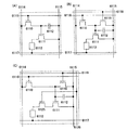
次に、本発明の作製方法を用いた発光装置の、画素の回路図について、図9を用いて説明する。図9(A)は、画素の等価回路図を示したものであり、信号線6114、電源線6115、6117、走査線6116、発光素子6113、画素へのビデオ信号の入力を制御するTFT6110、発光素子6113の両電極間に流れる電流値を制御するTFT6111、該TFT6111のゲート・ソース間電圧を保持する容量素子6112を有する。なお、図5(B)では、容量素子6112を図示したが、TFT6111のゲート容量や他の寄生容量で賄うことが可能な場合には、設けなくてもよい。
Next, a circuit diagram of a pixel of a light-emitting device using the manufacturing method of the present invention is described with reference to FIGS. FIG. 9A shows an equivalent circuit diagram of a pixel, which includes a
図9(B)は、図9(A)に示した画素に、TFT6118と走査線6119を新たに設けた構成の画素回路である。TFT6118の配置により、強制的に発光素子6113に電流が流れない状態を作ることができるため、全ての画素に対する信号の書き込みを待つことなく、書き込み期間の開始と同時又は直後に点灯期間を開始することができる。従って、デューティ比が向上して、動画の表示は特に良好に行なうことができる。
FIG. 9B illustrates a pixel circuit in which a
図9(C)は、図9(B)に示した画素に、新たにTFT6125と、配線6126を設けた画素回路である。本構成では、TFT6125のゲート電極を一定の電位に保持した配線6126に接続することにより、このゲート電極の電位を固定し、なおかつ飽和領域で動作させる。また、TFT6125と直列に接続させ、線形領域で動作するTFT6111のゲート電極には、TFT6110を介して、画素の点灯又は非点灯の情報を伝えるビデオ信号を入力する。線形領域で動作するTFT6111のソース・ドレイン間電圧の値は小さいため、TFT6111のゲート・ソース間電圧の僅かな変動は、発光素子6113に流れる電流値には影響を及ぼさない。従って、発光素子6113に流れる電流値は、飽和領域で動作するTFT6125により決定される。上記構成を有する本発明は、TFT6125の特性バラツキに起因した発光素子6113の輝度ムラを改善して画質を高めることができる。なお、TFT6125のチャネル長L1、チャネル幅W1、TFT6111のチャネル長L2、チャネル幅W2は、L1/W1:L2/W2=5〜6000:1を満たすように設定するとよい。また、両TFTは同じ導電型を有していると作製工程上好ましい。さらに、TFT6125には、エンハンスメント型だけでなく、ディプリーション型のTFTを用いてもよい。
FIG. 9C illustrates a pixel circuit in which a
なお、本発明を用いて形成された発光装置には、アナログのビデオ信号、デジタルのビデオ信号のどちらを用いてもよい。但し、デジタルのビデオ信号を用いる場合、そのビデオ信号が電圧を用いているものと、電流を用いているものとがある。つまり、発光素子の発光時において、画素に入力されるビデオ信号は、定電圧のものと、定電流のものがある。ビデオ信号が定電圧のものには、発光素子に印加される電圧が一定のものと、発光素子に流れる電流が一定のものとがある。またビデオ信号が定電流のものには、発光素子に印加される電圧が一定のものと、発光素子に流れる電流が一定のものとがある。この発光素子に印加される電圧が一定ならばは定電圧駆動であり、発光素子に流れる電流が一定ならばは定電流駆動である。定電流駆動は、発光素子の抵抗変化によらず、一定の電流が流れる。本発明の発光装置及びその駆動方法には、定電圧のビデオ信号、定電流のビデオ信号のどちらを用いてもよく、また定電圧駆動、定電流駆動のどちらを用いてもよい。本実施例は、上記の実施の形態、実施例と自由に組み合わせることができる。 Note that a light-emitting device formed using the present invention may use either an analog video signal or a digital video signal. However, when a digital video signal is used, there are a video signal using a voltage and a video signal using a current. That is, when the light emitting element emits light, a video signal input to the pixel includes a constant voltage signal and a constant current signal. A video signal having a constant voltage includes a constant voltage applied to the light emitting element and a constant current flowing through the light emitting element. In addition, a video signal having a constant current includes a constant voltage applied to the light emitting element and a constant current flowing in the light emitting element. When the voltage applied to the light emitting element is constant, constant voltage driving is performed. When the current flowing through the light emitting element is constant, constant current driving is performed. In constant current driving, a constant current flows regardless of the resistance change of the light emitting element. In the light emitting device and the driving method thereof according to the present invention, either a constant voltage video signal or a constant current video signal may be used, and either constant voltage driving or constant current driving may be used. This embodiment can be freely combined with the above embodiment modes and embodiments.
本発明が適用された発光装置の構成について、図10を用いて説明する。図10(A)は、発光装置の概略を説明する上面図であり、基板6200上に、画素部6201、信号線駆動回路6202、走査線駆動回路6203とを有している。6204は、基板6200上に形成された各種回路へ、信号または電源電位を供給するための入力端子に相当する。また、6205〜6207は保護回路であり、信号のノイズや静電気などにより素子が破壊されるのを防ぐ機能を有している。なお保護回路6205〜6207は全て設ける必要はなく、いずれか1つまたは複数を有していても良い。
A structure of a light-emitting device to which the present invention is applied will be described with reference to FIG. FIG. 10A is a top view illustrating an outline of a light-emitting device, which includes a
なお図10(A)では、画素部6201と同じ基板6200上に信号線駆動回路6202、走査線駆動回路6203を形成しているが、本発明はこの構成に限定されない。例えば、画素部6201を構成する半導体素子として、非晶質半導体又は微結晶半導体を用いる場合、別途形成した信号線駆動回路6202、走査線駆動回路6203をCOG方式やTAB方式等の公知の方式により基板6200に実装しても良い。なお、画素部6201を構成する素子として、微結晶半導体を用いる場合、走査線駆動回路と画素部とを同一基板上に微結晶半導体で形成し、信号線駆動回路は実装するようにしてもよい。また、走査線駆動回路の一部または信号線駆動回路の一部を、画素部と共に同一基板上に形成し、走査線駆動回路のほかの部分または信号線駆動回路の他の部分を実装するようにしても良い。つまり、駆動回路の形態は様々であり、本発明はいずれの構成を用いてもよい。
In FIG. 10A, the signal
次に、本発明を用いた発光装置に用いられる、保護回路6205〜6207の一例について説明する。保護回路は、TFT、ダイオード、抵抗素子及び容量素子等から選択された1つ又は複数の素子によって構成されるものであり、以下にはいくつかの保護回路の構成とその動作について説明する。
Next, an example of the
まず、入力端子と、基板上に形成された各種回路との間に配置される保護回路6205の構成について、図10(B)に示す等価回路図を用いて説明する。図10(B)に示す保護回路は、pチャネル型TFT7220、7230、容量素子7210、7240、抵抗素子7250を有する。抵抗素子7250は2端子の抵抗であり、一端には入力端子から与えられる入力電位Vinが、他端には低電位の電源電位VSSが与えられる。抵抗素子7250は、入力端子にVinが与えられなくなったときに、配線の電位をVSSに落とすために設けられており、その抵抗値は配線の配線抵抗よりも十分に大きくなるように設定する。
First, a structure of the
Vinが高電位の電源電位VDDよりも高い場合、そのゲート・ソース間電圧の関係から、TFT7220はオン、TFT7230はオフとなる。そうすると、VDDがTFT7220を介して、配線に与えられる。従って、雑音等により、VinがVDDよりも高くなっても、配線に与えられる電位は、VDDよりも高くなることはない。一方、VinがVSSよりも低い場合、そのゲート・ソース間電圧の関係から、TFT7220はオフ、TFT7230はオンとなる。そうすると、VSSが配線に与えられる。従って、雑音等により、VinがVSSよりも低くなっても、配線に与えられる電位は、VSSよりも低くなることはない。さらに、容量素子7210、7240により、入力端子からの電位にパルス状の雑音を鈍らせることができ、雑音による電位の急峻な変化をある程度小さくすることができる。
When Vin is higher than the high power supply potential VDD, the
上記構成の保護回路の配置により、配線の電位は、VSSとVDDの間に保たれ、この範囲外の異常に高いまたは低い電位の印加から、後段の回路を保護することができる。さらに、信号が入力される入力端子に保護回路を設けることで、信号が入力されていないときに、信号が与えられる全ての配線の電位を、一定(ここではVSS)の高さに保つことができる。つまり信号が入力されていないときは、配線同士をショートした状態にすることができるショートリングとしての機能も有する。そのため、配線間での電位差に起因する静電破壊を防ぐことができる。また、信号を入力しているときは、抵抗素子7250の抵抗値が十分に大きいので、配線に与えられる信号がVSSに引っ張られることがない。
With the arrangement of the protection circuit having the above structure, the potential of the wiring is kept between VSS and VDD, and the subsequent circuit can be protected from application of an abnormally high or low potential outside this range. Further, by providing a protective circuit at an input terminal to which a signal is input, the potentials of all wirings to which a signal is supplied can be kept constant (here, VSS) when no signal is input. it can. In other words, when a signal is not input, it also has a function as a short ring that can make the wirings short-circuited. Therefore, electrostatic breakdown due to a potential difference between wirings can be prevented. Further, when a signal is input, the resistance value of the
図10(C)は、pチャネル型TFT7220、7230を、整流性を有するダイオード7260、7270で代用した保護回路の等価回路図である。図10(D)は、pチャネル型TFT7220、7230を、TFT7350、7360、7370、7380で代用した保護回路の等価回路図である。
FIG. 10C is an equivalent circuit diagram of a protection circuit in which p-
また、上記とは別の構成の保護回路として図10(E)と図10(F)を示す。図10(E)に示す保護回路は、抵抗7280、7290と、nチャネル型TFT7300とを有する。図10(F)に示す保護回路は、抵抗7280、7290、pチャネル型TFT7310及びnチャネル型TFT7320を有する。図10(E)、図10(F)の両構成とも、端子7330には配線などが接続され、この配線などの電位が急激に変化した場合に、nチャネル型TFT7300、又はpチャネル型TFT7310及びnチャネル型TFT7320がオンすることで、電流を端子7330から7340の方向に流す。そうすると、端子7330に接続された電位の急激な変動を緩和し、素子の損傷又は破壊を防止することができる。なお、上記保護回路を構成する素子は、耐圧に優れた非晶質半導体により構成することが好ましい。本実施例は、上記の実施の形態と自由に組み合わせることが可能である。
FIG. 10E and FIG. 10F illustrate protection circuits having different structures from the above. A protection circuit illustrated in FIG. 10E includes
なお、信号線駆動回路6202と画素部6201の間は信号線によって接続されているが、保護回路6206は、ノイズや静電気などで該信号線の電位が急激に変動するのを防ぐことができる。また走査線駆動回路6203と画素部6201の間は走査線によって接続されているが、保護回路6207は、ノイズや静電気などで該走査線の電位が急激に変動するのを防ぐことができる。そして、保護回路6205と同様に、保護回路6206、6207も、図10(B)〜図10(F)に示す回路構成を用いることができる。
Note that although the signal
本実施例では、本発明を用いた発光装置の一形態に相当する、パネルの外観について、図11を用いて説明する。図11は、基板上に形成されたトランジスタ及び発光素子を、カバー材との間にシール材によって封止した、パネルの上面図であり、図11(B)は、図11(A)のA−A’における断面図に相当する。 In this example, the appearance of a panel corresponding to one mode of a light-emitting device using the present invention will be described with reference to FIGS. FIG. 11 is a top view of a panel in which a transistor and a light-emitting element formed over a substrate are sealed with a sealing material between the cover material and FIG. 11B is a top view of FIG. 11A. This corresponds to a cross-sectional view at −A ′.
基板4001上に設けられた画素部4002と、信号線駆動回路4003と、走査線駆動回路4004とを囲むようにして、シール材4005が設けられている。また画素部4002と、信号線駆動回路4003と、走査線駆動回路4004の上にカバー材4006が設けられている。よって画素部4002と、信号線駆動回路4003と、走査線駆動回路4004とは、基板4001とシール材4005とカバー材4006とによって、充填材4007と共に密封されている。
A
また基板4001上に設けられた画素部4002と、信号線駆動回路4003と、走査線駆動回路4004は、トランジスタを複数有しており、図11(B)では、信号線駆動回路4003に含まれるトランジスタ4008、4009と、画素部4002に含まれるトランジスタ4010とを示す。
In addition, the
また4011は発光素子に相当し、トランジスタ4010と電気的に接続されている。
また引き回し配線4014は、画素部4002と、信号線駆動回路4003と、走査線駆動回路4004に、信号または電源電圧を供給するための配線に相当する。引き回し配線4014は、引き回し配線4015を介して接続端子4016と接続されている。接続端子4016は、FPC4018が有する端子と、異方性導電膜4019を介して電気的に接続されている。
The
なお、基板4001としては、ガラス、金属(代表的にはステンレス)、セラミックスのほか、プラスチックに代表されるようなフレキシブルな素材を用いることができる。プラスチックとしては、FRP(Fiberglass−Reinforced Plastics)板、PVF(ポリビニルフルオライド)フィルム、マイラーフィルム、ポリエステルフィルムまたはアクリル樹脂フィルムを用いることができる。また、アルミニウムホイルをPVFフィルムやマイラーフィルムで挟んだ構造のシートを用いることもできる。またカバー材4006は、ガラス板、プラスチック板、ポリエステルフィルムまたはアクリルフィルムのような透光性を有する材料を用いる。
Note that as the
また、充填材4007としては窒素やアルゴンなどの不活性な気体の他に、紫外線硬化樹脂または熱硬化樹脂を用いることができ、PVC(ポリビニルクロライド)、アクリル、ポリイミド、エポキシ樹脂、シリコン樹脂、PVB(ポリビニルブチラル)またはEVA(エチレンビニルアセテート)を用いることができる。本実施例では充填材として窒素を用いた。
As the
また充填材4007を吸湿性物質(好ましくは酸化バリウム)もしくは酸素を吸着しうる物質にさらしておいても良い。
Alternatively, the
本発明の発光装置は、消費電力の割に外部量子効率が高く、画像のコントラストを高めることができる。従って、太陽光などの外光が照射されていても、消費電力をおさえつつ鮮明な画像を表示することができるため、使用場所を比較的選ばずに使用できるところがメリットとして大きい。従って、テレビなどの他、携帯用の電子機器などに非常に適している。 The light emitting device of the present invention has high external quantum efficiency for power consumption, and can increase the contrast of an image. Therefore, even if external light such as sunlight is irradiated, a clear image can be displayed while suppressing power consumption. Therefore, the advantage is that it can be used without relatively selecting a place of use. Therefore, it is very suitable for portable electronic devices as well as televisions.
具体的に本発明の発光装置を用いた電子機器として、ビデオカメラ、デジタルカメラ、ゴーグル型ディスプレイ(ヘッドマウントディスプレイ)、ナビゲーションシステム、音響再生装置(カーオーディオ、オーディオコンポ等)、ノート型パーソナルコンピュータ、ゲーム機器、携帯情報端末(モバイルコンピュータ、携帯電話、携帯型ゲーム機または電子書籍等)、記録媒体を備えた画像再生装置(具体的にはDVD(Digital Versatile Disc))等の記録媒体を再生し、その画像を表示しうるディスプレイを備えた装置)などが挙げられる。これら電子機器の具体例を図12に示す。 Specifically, as an electronic device using the light emitting device of the present invention, a video camera, a digital camera, a goggle type display (head mounted display), a navigation system, a sound reproduction device (car audio, audio component, etc.), a notebook type personal computer, Plays back recording media such as game machines, portable information terminals (mobile computers, mobile phones, portable game machines, electronic books, etc.), and image playback devices (specifically DVDs (Digital Versatile Disc)) equipped with recording media. And a device provided with a display capable of displaying the image). Specific examples of these electronic devices are shown in FIGS.
図12(A)は表示装置であり、筐体2001、支持台2002、表示部2003、スピーカー部2004、ビデオ入力端子2005等を含む。本発明の発光装置は、表示部2003に用いることができる。発光装置は自発光型であるためバックライトが必要なく、液晶ディスプレイよりも薄い表示部とすることができる。なお、発光素子を用いた表示装置は、パーソナルコンピューター用、TV放送受信用、広告表示用などの全ての情報表示用表示装置が含まれる。
FIG. 12A illustrates a display device, which includes a
図12(B)はノート型パーソナルコンピュータであり、本体2201、筐体2202、表示部2203、キーボード2204、外部接続ポート2205、マウス2206等を含む。本発明の発光装置は、表示部2203に用いることができる。
FIG. 12B illustrates a laptop personal computer, which includes a
図12(C)は携帯情報端末(PDA)であり、本体2101、表示部2102、操作キー2103、モデム2104等を含む。モデム2104は本体2101に内蔵されていても良い。本発明の発光装置は、表示部2102に用いることができる。
FIG. 12C illustrates a personal digital assistant (PDA), which includes a
以上の様に、本発明の適用範囲は極めて広く、あらゆる分野の電子機器に用いることが可能である。また、本実施例の電子機器は、実施例1〜4に示したいずれの構成の発光装置を用いても良い。
As described above, the applicable range of the present invention is so wide that it can be used for electronic devices in various fields. In addition, the electronic device of this embodiment may use the light emitting device having any structure shown in
本発明の発光装置に用いられるトランジスタは、多結晶半導体を用いたTFTであっても良いし、アモルファス半導体またはセミアモルファス半導体を用いたTFTであっても良い。本実施例では、アモルファス半導体またはセミアモルファス半導体を用いて形成されたTFTの構成について説明する。 The transistor used in the light emitting device of the present invention may be a TFT using a polycrystalline semiconductor, or a TFT using an amorphous semiconductor or a semi-amorphous semiconductor. In this embodiment, a structure of a TFT formed using an amorphous semiconductor or a semi-amorphous semiconductor will be described.
図7(A)に、駆動回路に用いられるTFTの断面図と、画素部に用いられるTFTの断面図を示す。1001は駆動回路に用いられるTFTの断面図に相当し、1002は画素部に用いられるTFTの断面図に相当し、1003は該TFT1002によって電流が供給される発光素子の断面図に相当する。TFT1001、1002は逆スタガ型(ボトムゲート型)である。
FIG. 7A shows a cross-sectional view of a TFT used for a driver circuit and a cross-sectional view of a TFT used for a pixel portion. 1001 corresponds to a cross-sectional view of a TFT used in a driver circuit, 1002 corresponds to a cross-sectional view of a TFT used in a pixel portion, and 1003 corresponds to a cross-sectional view of a light-emitting element to which current is supplied by the
駆動回路のTFT1001は、基板1000上に形成されたゲート電極1010と、ゲート電極1010を覆っているゲート絶縁膜1011と、ゲート絶縁膜1011を間に挟んでゲート電極1010と重なっている、セミアモルファス半導体またはアモルファス半導体で形成された第1の半導体膜1012とを有している。さらにTFT1001は、ソース領域またはドレイン領域として機能する一対の第2の半導体膜1013と、第1の半導体膜1012と第2の半導体膜1013の間に設けられた第3の半導体膜1014とを有している。
The
図7(A)では、ゲート絶縁膜1011が2層の絶縁膜で形成されているが、本発明はこの構成に限定されない。ゲート絶縁膜1011が単層または3層以上の絶縁膜で形成されていても良い。
In FIG. 7A, the
また第2の半導体膜1013は、アモルファス半導体またはセミアモルファス半導体で形成されており、該半導体膜に一導電型を付与する不純物が添加されている。そして一対の第2の半導体膜1013は、第1の半導体膜1012のチャネルが形成される領域を間に挟んで、向かい合っている。
The
また第3の半導体膜1014は、アモルファス半導体またはセミアモルファス半導体で形成されており、第2の半導体膜1013と同じ導電型を有し、なおかつ第2の半導体膜1013よりも導電性が低くなるような特性を有している。第3の半導体膜1014はLDD領域として機能するので、ドレイン領域として機能する第2の半導体膜1013の端部に集中する電界を緩和し、ホットキャリア効果を防ぐことができる。第3の半導体膜1014は必ずしも設ける必要はないが、設けることでTFTの耐圧性を高め、信頼性を向上させることができる。なお、TFT1001がn型である場合、第3の半導体膜1014を形成する際に特にn型を付与する不純物を添加せずとも、n型の導電型が得られる。よって、TFT1001がn型の場合、必ずしも第3の半導体膜1014にn型の不純物を添加する必要はない。ただし、チャネルが形成される第1の半導体膜には、p型の導電性を付与する不純物を添加し、極力I型に近づくようにその導電型を制御しておく。
The
また、一対の第2の半導体膜1013に接するように、2つの配線1015が形成されている。
In addition, two
駆動回路のTFT1002は、基板1000上に形成されたゲート電極1020と、ゲート電極1020を覆っているゲート絶縁膜1011と、ゲート絶縁膜1011を間に挟んでゲート電極1020と重なっている、アモルファス半導体またはセミアモルファス半導体で形成された第1の半導体膜1022とを有している。さらにTFT1002は、ソース領域またはドレイン領域として機能する一対の第2の半導体膜1023と、第1の半導体膜1022と第2の半導体膜1023の間に設けられた第3の半導体膜1024とを有している。
The
また第2の半導体膜1023は、アモルファス半導体またはセミアモルファス半導体で形成されており、該半導体膜に一導電型を付与する不純物が添加されている。そして一対の第2の半導体膜1023は、第1の半導体膜1022のチャネルが形成される領域を間に挟んで、向かい合っている。
The
また第3の半導体膜1024は、アモルファス半導体またはセミアモルファス半導体で形成されており、第2の半導体膜1023と同じ導電型を有し、なおかつ第2の半導体膜1023よりも導電性が低くなるような特性を有している。第3の半導体膜1024はLDD領域として機能するので、ドレイン領域として機能する第2の半導体膜1023の端部に集中する電界を緩和し、ホットキャリア効果を防ぐことができる。第3の半導体膜1024は必ずしも設ける必要はないが、設けることでTFTの耐圧性を高め、信頼性を向上させることができる。なお、TFT1002がn型である場合、第3の半導体膜1024を形成する際に特にn型を付与する不純物を添加せずとも、n型の導電型が得られる。よって、TFT1002がn型の場合、必ずしも第3の半導体膜1024にn型の不純物を添加する必要はない。ただし、チャネルが形成される第1の半導体膜には、p型の導電性を付与する不純物を添加し、極力I型に近づくようにその導電型を制御しておく。
The
また、一対の第2の半導体膜1023に接するように、配線1025が形成されている。
A
また、TFT1001、1002及び配線1015、1025を覆うように、絶縁膜からなる第1のパッシベーション膜1040、第2のパッシベーション膜1041が形成されている。TFT1001、1002を覆うパッシベーション膜は2層に限らず、単層であっても良いし、3層以上であっても良い。例えば第1のパッシベーション膜1040を窒化珪素、第2のパッシベーション膜1041を酸化珪素で形成することができる。窒化珪素または窒化酸化珪素でパッシベーション膜を形成することで、TFT1001、1002が水分や酸素などの影響により、劣化するのを防ぐことができる。
A
そして、配線1025の一方は、発光素子1003の陽極1030に接続されている。また陽極1030上に接するように、電界発光層1031が、該電界発光層1031に接するように陰極1032が形成されている。
One end of the
陽極1030は、透光性酸化物導電層1030aとバリア層1030bとを有しており、バリア層1030bは、電界発光層1031と接している。
The
次に、本発明の発光装置が有するTFTの、図7(A)とは異なる形態について説明する。図7(B)に、駆動回路に用いられるTFTの断面図と、画素部に用いられるTFTの断面図を示す。1101は駆動回路に用いられるTFTの断面図に相当し、1102は画素部に用いられるTFTの断面図に相当し、1103は、該TFT1102によって電流が供給される発光素子の断面図に相当する。
Next, a mode different from that in FIG. 7A of the TFT included in the light-emitting device of the present invention is described. FIG. 7B shows a cross-sectional view of a TFT used for a driver circuit and a cross-sectional view of a TFT used for a pixel portion. 1101 corresponds to a cross-sectional view of a TFT used in a driver circuit, 1102 corresponds to a cross-sectional view of a TFT used in a pixel portion, and 1103 corresponds to a cross-sectional view of a light-emitting element to which current is supplied by the
駆動回路のTFT1101と画素部のTFT1102は、基板1100上に形成されたゲート電極1110、1120と、ゲート電極1110、1120を覆っているゲート絶縁膜1111と、ゲート絶縁膜1111を間に挟んでゲート電極1110、1120と重なっている、アモルファス半導体またはセミアモルファス半導体で形成された第1の半導体膜1112、1122とをそれぞれ有している。そして、第1の半導体膜1112、1122のチャネル形成領域を覆うように、絶縁膜で形成されたチャネル保護膜1133、1134が形成されている。チャネル保護膜1133、1134は、TFT1101、1102の作製工程において、第1の半導体膜1112、1122のチャネル形成領域がエッチングされてしまうのを防ぐために設ける。さらにTFT1101、1102は、ソース領域またはドレイン領域として機能する一対の第2の半導体膜1113、1123と、第1の半導体膜1112、1122と第2の半導体膜1113、1123の間に設けられた第3の半導体膜1114、1124とをそれぞれ有している。
The
図7(B)では、ゲート絶縁膜1111が2層の絶縁膜で形成されているが、本発明はこの構成に限定されない。ゲート絶縁膜1111が単層または3層以上の絶縁膜で形成されていても良い。
In FIG. 7B, the
また第2の半導体膜1113、1123は、アモルファス半導体またはセミアモルファス半導体で形成されており、該半導体膜に一導電型を付与する不純物が添加されている。そして一対の第2の半導体膜1113、1123は、第1の半導体膜1112、1122のチャネルが形成される領域を間に挟んで、向かい合っている。
The
また第3の半導体膜1114、1124は、アモルファス半導体またはセミアモルファス半導体で形成されており、第2の半導体膜1113、1123と同じ導電型を有し、なおかつ第2の半導体膜1113、1123よりも導電性が低くなるような特性を有している。第3の半導体膜1114、1124はLDD領域として機能するので、ドレイン領域として機能する第2の半導体膜1113、1123の端部に集中する電界を緩和し、ホットキャリア効果を防ぐことができる。第3の半導体膜1114、1124は必ずしも設ける必要はないが、設けることでTFTの耐圧性を高め、信頼性を向上させることができる。なお、TFT1101、1102がn型である場合、第3の半導体膜1114、1124を形成する際に特にn型を付与する不純物を添加せずとも、n型の導電型が得られる。よって、TFT1101、1102がn型の場合、必ずしも第3の半導体膜1114、1124にn型の不純物を添加する必要はない。ただし、チャネルが形成される第1の半導体膜には、p型の導電性を付与する不純物を添加し、極力I型に近づくようにその導電型を制御しておく。
In addition, the
また、一対の第2の半導体膜1113、1123に接するように、2つの配線1115と、2つの配線1125が形成されている。
In addition, two
また、TFT1101、1102及び配線1115、1125を覆うように、絶縁膜からなる第1のパッシベーション膜1140、第2のパッシベーション膜1141が形成されている。TFT1101、1102を覆うパッシベーション膜は2層に限らず、単層であっても良いし、3層以上であっても良い。例えば第1のパッシベーション膜1140を窒化珪素、第2のパッシベーション膜1141を酸化珪素で形成することができる。窒化珪素または窒化酸化珪素でパッシベーション膜を形成することで、TFT1101、1102が水分や酸素などの影響により、劣化するのを防ぐことができる。
A
そして、配線1125の一方は、発光素子1103の陽極1130に接続されている。また陽極1130上に接するように、電界発光層1131が、該電界発光層1131に接するように陰極1132が形成されている。
One end of the
陽極1130は、透光性酸化物導電層1130aとバリア層1130bとを有しており、バリア層1130bは、電界発光層1131と接している。
The
なお本実施例では、アモルファス半導体またはセミアモルファス半導体を用いたTFTで発光装置の駆動回路と画素部を同じ基板上に形成した例について説明したが、本発明はこの構成に限定されない。アモルファス半導体またはセミアモルファス半導体を用いたTFTで画素部を形成し、該画素部が形成された基板に別途形成された駆動回路を貼り付けても良い。 Note that in this embodiment, an example in which a driver circuit of a light-emitting device and a pixel portion are formed over the same substrate using a TFT using an amorphous semiconductor or a semi-amorphous semiconductor is described; however, the present invention is not limited to this structure. A pixel portion may be formed using a TFT using an amorphous semiconductor or a semi-amorphous semiconductor, and a separately formed driver circuit may be attached to a substrate on which the pixel portion is formed.
またゲート電極や配線などを液滴吐出法で形成しても良い。図13(A)に、液滴吐出法を用いて形成された画素の断面図を一例として示す。図13(A)において1201はボトムゲート型のTFTであり、発光素子1202と電気的に接続されている。TFT1201は、ゲート電極1203と、ゲート電極1203上に形成されたゲート絶縁膜1204と、ゲート絶縁膜1204上に形成された第1の半導体膜1205と、前記第1の半導体膜1205上に形成された第2の半導体膜1206とを有している。なお第1の半導体膜1205はチャネル形成領域として機能する。そして第2の半導体膜1206には、導電型を付与する不純物が添加されており、ソース領域またはドレイン領域として機能する。
Further, a gate electrode, a wiring, or the like may be formed by a droplet discharge method. FIG. 13A illustrates a cross-sectional view of a pixel formed using a droplet discharge method as an example. In FIG. 13A,
また第2の半導体膜1206に接するように配線1208が形成されており、配線1208は、発光素子1202が有する陽極1209と接続されている。また発光素子1202は、陽極1209と、前記陽極1209上に形成された電界発光層1210と、前記電界発光層1210上に形成された陰極1211とを有している。陽極1209は、透光性酸化物導電層1209aとバリア層1209bとを有している。
A
図13(A)に示す発光装置では、ゲート電極1203、配線1208、陽極1209、電界発光層1210、パターン形成に用いるマスクなどを、液滴吐出法を用いて形成することができる。
In the light-emitting device illustrated in FIG. 13A, the
また図13(B)に、液滴吐出法を用いて形成された画素の断面図を一例として示す。図13(B)では、ボトムゲート型のTFT1220が有する第1の半導体膜1221上に、第2の半導体膜1222及び配線1223をパターニングする際に、第1の半導体膜1221がエッチングされてしまうのを防ぐことができる絶縁膜(エッチングストッパー)1224が形成されている。
FIG. 13B illustrates an example of a cross-sectional view of a pixel formed using a droplet discharge method. In FIG. 13B, the
本実施例では、絶縁膜と、当該絶縁膜上に形成された陽極との組み合わせについて説明する。 In this embodiment, a combination of an insulating film and an anode formed over the insulating film will be described.
図14(A)に、絶縁膜として窒化酸化珪素を用い、該絶縁膜上に5重量%の酸化珪素を含むITSOを用いて陽極を形成した発光素子の、輝度L(cd/m2)に対する電流効率η(cd/A)の実測値を示す。また比較として図14(A)に、絶縁膜として同じく窒化酸化珪素を用い、該絶縁膜上にITOを用いて陽極を形成した発光素子の、輝度L(cd/m2)に対する電流効率η(cd/A)の実測値を示す。 FIG. 14A shows the luminance L (cd / m 2 ) of a light-emitting element in which silicon nitride oxide is used as an insulating film and an anode is formed using ITSO containing 5% by weight of silicon oxide on the insulating film. The measured value of current efficiency η (cd / A) is shown. For comparison, FIG. 14A also shows current efficiency η (for luminance L (cd / m 2 ) of a light-emitting element in which silicon nitride oxide is also used as an insulating film and an anode is formed on the insulating film using ITO. The actual measurement value of cd / A) is shown.
なお図14(A)に示す測定で用いたサンプルは、窒化酸化珪素を用いた絶縁膜を、シロキサン系材料を出発材料として形成されたSi−O結合とSi−CHX結合手を含む、膜厚0.8μmの絶縁膜上に形成している。そして、窒化酸化珪素を用いた絶縁膜は、CVD法で、100nmの膜厚で形成している。 Note that the sample used in the measurement illustrated in FIG. 14A is an insulating film using silicon nitride oxide, which includes a Si—O bond and a Si—CH X bond formed using a siloxane-based material as a starting material. It is formed on an insulating film having a thickness of 0.8 μm. The insulating film using silicon nitride oxide is formed with a thickness of 100 nm by a CVD method.
図14(A)に示すように、陽極にITSOを用いたサンプルの方が、陽極にITOを用いたサンプルよりも、電流効率が高いことが分かった。 As shown in FIG. 14A, it was found that the sample using ITSO for the anode had higher current efficiency than the sample using ITO for the anode.
次に図14(B)に、絶縁膜として窒化珪素を用い、該絶縁膜上に5重量%の酸化珪素を含むITSOを用いて陽極を形成した発光素子の、輝度L(cd/m2)に対する電流効率η(cd/A)の実測値を示す。また比較として図14(B)に、絶縁膜として同じく窒化珪素を用い、該絶縁膜上にITOを用いて陽極を形成した発光素子の、輝度L(cd/m2)に対する電流効率η(cd/A)の実測値を示す。 Next, FIG. 14B shows luminance L (cd / m 2 ) of a light-emitting element in which silicon nitride is used as an insulating film and an anode is formed on the insulating film using ITSO containing 5 wt% silicon oxide. The measured value of the current efficiency η (cd / A) with respect to is shown. For comparison, FIG. 14B shows a current efficiency η (cd) with respect to luminance L (cd / m 2 ) of a light-emitting element in which silicon nitride is also used as an insulating film and an anode is formed on the insulating film using ITO. / A) shows the actual measured value.
なお図14(B)に示す測定で用いたサンプルは、窒化珪素を用いた絶縁膜を、膜厚0.8μmのアクリルを含む絶縁膜上に形成している。そして、窒化珪素を用いた絶縁膜は、スパッタ法で、100nmの膜厚で形成している。 Note that in the sample used in the measurement illustrated in FIG. 14B, an insulating film using silicon nitride is formed over an insulating film containing acrylic with a thickness of 0.8 μm. The insulating film using silicon nitride is formed with a thickness of 100 nm by sputtering.
図14(B)に示すように、図14(A)と同様に、陽極にITSOを用いたサンプルの方が、陽極にITOを用いたサンプルよりも、電流効率が高いことが分かった。 As shown in FIG. 14B, as in FIG. 14A, the sample using ITSO for the anode was found to have higher current efficiency than the sample using ITO for the anode.
次に図14(C)に、絶縁膜として酸化珪素を用い、該絶縁膜上に5重量%の酸化珪素を含むITSOを用いて陽極を形成した発光素子の、輝度L(cd/m2)に対する電流効率η(cd/A)の実測値を示す。また比較として図14(C)に、絶縁膜として同じく酸化珪素を用い、該絶縁膜上にITOを用いて陽極を形成した発光素子の、輝度L(cd/m2)に対する電流効率η(cd/A)の実測値を示す。 Next, FIG. 14C illustrates a luminance L (cd / m 2 ) of a light-emitting element in which silicon oxide is used as an insulating film and an anode is formed using ITSO containing 5 wt% silicon oxide on the insulating film. The measured value of the current efficiency η (cd / A) with respect to is shown. For comparison, FIG. 14C shows a current efficiency η (cd) with respect to luminance L (cd / m 2 ) of a light-emitting element in which silicon oxide is also used as an insulating film and an anode is formed using ITO on the insulating film. / A) shows the actual measured value.
なお図14(C)に示す測定で用いたサンプルは、酸化珪素を用いた絶縁膜を、100nmの膜厚で形成している。 Note that in the sample used in the measurement illustrated in FIG. 14C, an insulating film using silicon oxide is formed with a thickness of 100 nm.
図14(A)、図14(B)と、図14(C)を比較すると、陽極にITSOを用いた場合、絶縁膜として酸化珪素を用いるよりも、窒化酸化珪素または窒化珪素を用いた方が、高い電流効率が得られ、結果的には高い内部量子効率が得られることが分かる。 14A and 14B are compared with FIG. 14C, when ITSO is used for the anode, silicon nitride oxide or silicon nitride is used rather than silicon oxide as the insulating film. However, it can be seen that high current efficiency is obtained, and as a result, high internal quantum efficiency is obtained.
なお図14では、ITSOを用いた単層の陽極の場合について示しているが、上記構成を本発明の構成と組み合わせることで、より発光装置の内部量子効率を高められると考えられる。すなわち、窒化珪素または窒化酸化珪素を含む絶縁膜上に、透光性酸化物導電層及びバリア層を有する陽極と、電界発光層と、陰極とを順に積層することで、より高い内部量子効率を得ることができる。 Note that FIG. 14 illustrates the case of a single-layer anode using ITSO, but it is considered that the internal quantum efficiency of the light-emitting device can be further increased by combining the above structure with the structure of the present invention. That is, by stacking an anode having a light-transmitting oxide conductive layer and a barrier layer, an electroluminescent layer, and a cathode in this order on an insulating film containing silicon nitride or silicon nitride oxide, higher internal quantum efficiency can be obtained. Obtainable.
100 基板
101 陽極
102 電界発光層
103 陰極
104 第1の層
105 第2の層
106 第3の層
107 第4の層
108 第5の層
109a バリア層
109b 透光性酸化物導電層
110 基板
111 陽極
112 電界発光層
113 陰極
114 Al−Si層
115 Ti層
116 透光性酸化物導電層
117 バリア層
201 基板
202 下地膜
203 半導体膜
204 半導体膜
205 nチャネル型TFT
206 pチャネル型TFT
207 ゲート絶縁膜
208 ゲート電極
209 ゲート電極
210 パッシベーション膜
211 第1の層間絶縁膜
212 第2の層間絶縁膜
213 配線
214 配線
215 配線
216 配線
217 透光性酸化物導電層
218 バリア層
219 陽極
220 パターニング後の透光性酸化物導電層
221 パターニング後のバリア層
222 隔壁
223 電界発光層
224 陰極
225 発光素子
7000 基板
7001 トランジスタ
7002 トランジスタ
7003 トランジスタ
7004 第1の層間絶縁膜
7005 配線
7006 配線
7007 配線
7008 第2の層間絶縁膜
7009 第3の層間絶縁膜
7010 配線
7011 配線
7012 配線
7013 透光性酸化物導電層
7014 透光性酸化物導電層
7015 透光性酸化物導電層
7016 バリア層
7017 バリア層
7018 バリア層
7019 陽極
7020 陽極
7021 陽極
7022 電界発光層
7023 電界発光層
7024 電界発光層
7025 陰極
7026 発光素子
7027 発光素子
7028 発光素子
7030 カバー材
7031 遮蔽膜
7032 着色層
7033 着色層
7034 着色層
7035 カラーフィルター
7040 隔壁
6110 TFT
6111 TFT
6112 容量素子
6113 発光素子
6114 信号線
6115 電源線
6116 走査線
6117 電源線
6118 TFT
6119 走査線
6125 TFT
6126 配線
6200 基板
6201 画素部
6202 信号線駆動回路
6203 走査線駆動回路
6204 入力端子
6205 保護回路
6206 保護回路
6207 保護回路
7210 容量素子
7220 pチャネル型TFT
7230 TFT
7240 容量素子
7250 抵抗素子
7260 ダイオード
7270 ダイオード
7280 抵抗
7290 抵抗
7300 nチャネル型TFT
7310 pチャネル型TFT
7320 nチャネル型TFT
7330 端子
7340 端子
7350 TFT
7360 TFT
7370 TFT
7380 TFT
4001 基板
4002 画素部
4003 信号線駆動回路
4004 走査線駆動回路
4005 シール材
4006 カバー材
4007 充填材
4008 トランジスタ
4009 トランジスタ
4010 トランジスタ
4011 発光素子
4014 配線
4015 配線
4016 接続端子
4018 FPC
4019 異方性導電膜
2001 筐体
2002 支持台
2003 表示部
2004 スピーカー部
2005 ビデオ入力端子
2201 本体
2202 筐体
2203 表示部
2204 キーボード
2205 外部接続ポート
2206 マウス
2101 本体
2102 表示部
2103 操作キー
2104 モデム
1000 基板
1001 TFT
1002 TFT
1003 発光素子
1010 ゲート電極
1011 ゲート絶縁膜
1012 第1の半導体膜
1013 第2の半導体膜
1014 第3の半導体膜
1015 配線
1020 ゲート電極
1022 第1の半導体膜
1023 第2の半導体膜
1024 第3の半導体膜
1025 配線
1030 陽極
1030a 透光性酸化物導電層
1030b バリア層
1031 電界発光層
1032 陰極
1040 パッシベーション膜
1041 パッシベーション膜
1100 基板
1101 TFT
1102 TFT
1103 発光素子
1110 ゲート電極
1111 ゲート絶縁膜
1112 第1の半導体膜
1113 第2の半導体膜
1114 第3の半導体膜
1115 配線
1120 ゲート電極
1122 第1の半導体膜
1123 第2の半導体膜
1124 第3の半導体膜
1125 配線
1130 チャネル保護膜
1131 チャネル保護膜
1132 陰極
1133 陽極
1133a 透光性酸化物導電層
1133b バリア層
1134 電界発光層
1140 パッシベーション膜
1141 パッシベーション膜
1201 TFT
1202 発光素子
1203 ゲート電極
1204 ゲート絶縁膜
1205 第1の半導体膜
1206 第2の半導体膜
1208 配線
1209 陽極
1210 電界発光層
1211 陰極
1209a 透光性酸化物導電層
1209b バリア層
1220 TFT
1221 第1の半導体膜
1222 第2の半導体膜
1223 配線
1224 絶縁膜
100
206 p-channel TFT
207
6111 TFT
6112
6119
6126
7230 TFT
7240
7310 p-channel TFT
7320 n-channel TFT
7330
7360 TFT
7370 TFT
7380 TFT
4001
4019 Anisotropic
1002 TFT
1003
1102 TFT
1103
1202
1221
Claims (3)
前記陽極上に形成された電界発光層と、
前記電界発光層上に形成された陰極とを有し、
前記絶縁膜は、窒素及び珪素を含んでおり、
前記陽極は、前記絶縁膜に接する透光性酸化物導電層と、前記電界発光層に接する0.5〜5nmの厚さのバリア層とを有し、
前記透光性酸化物導電層及び前記バリア層は、酸化インジウムスズ及び酸化珪素を含んでおり、
前記透光性酸化物導電層における珪素の密度よりも前記バリア層における珪素の密度の方が高く、
前記バリア層は、前記電界発光層に含まれる正孔注入層と接していることを特徴とする発光装置。 An anode formed in contact with an insulating film using silicon nitride oxide;
An electroluminescent layer formed on the anode;
A cathode formed on the electroluminescent layer,
The insulating film contains nitrogen and silicon;
The anode has a light-transmitting oxide conductive layer in contact with the insulating film, and a barrier layer having a thickness of 0.5 to 5 nm in contact with the electroluminescent layer,
The translucent oxide conductive layer and the barrier layer contain indium tin oxide and silicon oxide,
The silicon density in the barrier layer is higher than the silicon density in the translucent oxide conductive layer,
The light-emitting device, wherein the barrier layer is in contact with a hole injection layer included in the electroluminescent layer.
Priority Applications (1)
| Application Number | Priority Date | Filing Date | Title |
|---|---|---|---|
| JP2004299587A JP4704004B2 (en) | 2003-10-20 | 2004-10-14 | LIGHT EMITTING DEVICE AND ELECTRONIC DEVICE |
Applications Claiming Priority (3)
| Application Number | Priority Date | Filing Date | Title |
|---|---|---|---|
| JP2003359778 | 2003-10-20 | ||
| JP2003359778 | 2003-10-20 | ||
| JP2004299587A JP4704004B2 (en) | 2003-10-20 | 2004-10-14 | LIGHT EMITTING DEVICE AND ELECTRONIC DEVICE |
Publications (3)
| Publication Number | Publication Date |
|---|---|
| JP2005150097A JP2005150097A (en) | 2005-06-09 |
| JP2005150097A5 JP2005150097A5 (en) | 2007-11-15 |
| JP4704004B2 true JP4704004B2 (en) | 2011-06-15 |
Family
ID=34703019
Family Applications (1)
| Application Number | Title | Priority Date | Filing Date |
|---|---|---|---|
| JP2004299587A Expired - Fee Related JP4704004B2 (en) | 2003-10-20 | 2004-10-14 | LIGHT EMITTING DEVICE AND ELECTRONIC DEVICE |
Country Status (1)
| Country | Link |
|---|---|
| JP (1) | JP4704004B2 (en) |
Families Citing this family (3)
| Publication number | Priority date | Publication date | Assignee | Title |
|---|---|---|---|---|
| JP5001745B2 (en) * | 2007-08-10 | 2012-08-15 | 住友化学株式会社 | Organic electroluminescence device and manufacturing method |
| JP2009044104A (en) * | 2007-08-10 | 2009-02-26 | Sumitomo Chemical Co Ltd | Organic electroluminescence element and manufacturing method thereof |
| CN105428554B (en) * | 2015-12-21 | 2018-02-13 | 广东聚华印刷显示技术有限公司 | One kind printing OLED and preparation method thereof |
Citations (4)
| Publication number | Priority date | Publication date | Assignee | Title |
|---|---|---|---|---|
| JP2001312223A (en) * | 2000-02-22 | 2001-11-09 | Semiconductor Energy Lab Co Ltd | Spontaneous light emitting device and method for manufacturing the same |
| JP2002175879A (en) * | 2000-12-08 | 2002-06-21 | Tdk Corp | Organic el display panel and organic el element using the same |
| JP2003114626A (en) * | 2001-06-18 | 2003-04-18 | Semiconductor Energy Lab Co Ltd | Light emitting device and method for manufacturing the same |
| JP2003297551A (en) * | 2002-03-29 | 2003-10-17 | Pioneer Electronic Corp | Organic electroluminescence display panel |
Family Cites Families (1)
| Publication number | Priority date | Publication date | Assignee | Title |
|---|---|---|---|---|
| JP3067949B2 (en) * | 1994-06-15 | 2000-07-24 | シャープ株式会社 | Electronic device and liquid crystal display device |
-
2004
- 2004-10-14 JP JP2004299587A patent/JP4704004B2/en not_active Expired - Fee Related
Patent Citations (4)
| Publication number | Priority date | Publication date | Assignee | Title |
|---|---|---|---|---|
| JP2001312223A (en) * | 2000-02-22 | 2001-11-09 | Semiconductor Energy Lab Co Ltd | Spontaneous light emitting device and method for manufacturing the same |
| JP2002175879A (en) * | 2000-12-08 | 2002-06-21 | Tdk Corp | Organic el display panel and organic el element using the same |
| JP2003114626A (en) * | 2001-06-18 | 2003-04-18 | Semiconductor Energy Lab Co Ltd | Light emitting device and method for manufacturing the same |
| JP2003297551A (en) * | 2002-03-29 | 2003-10-17 | Pioneer Electronic Corp | Organic electroluminescence display panel |
Also Published As
| Publication number | Publication date |
|---|---|
| JP2005150097A (en) | 2005-06-09 |
Similar Documents
| Publication | Publication Date | Title |
|---|---|---|
| US9034675B2 (en) | Light-emitting device and method for manufacturing light-emitting device | |
| US10490618B2 (en) | Light emitting device | |
| KR101258421B1 (en) | Light emitting device and electronic device | |
| JP5063799B2 (en) | Light emitting element and display device | |
| JP5031115B2 (en) | Display device | |
| JP5165041B2 (en) | Light emitting device | |
| JP4890117B2 (en) | Light emitting device and manufacturing method thereof | |
| JP5078267B2 (en) | Light emitting device | |
| JP2012074398A (en) | Light-emitting device | |
| JP4731865B2 (en) | Light emitting device | |
| JP4823566B2 (en) | Light emitting element, display device, and television receiver | |
| JP4817730B2 (en) | Display device | |
| JP4704004B2 (en) | LIGHT EMITTING DEVICE AND ELECTRONIC DEVICE | |
| JP4588312B2 (en) | Method for manufacturing light emitting device | |
| JP4637472B2 (en) | Method for manufacturing light emitting device | |
| JP5084123B2 (en) | Light emitting device |
Legal Events
| Date | Code | Title | Description |
|---|---|---|---|
| A521 | Request for written amendment filed |
Free format text: JAPANESE INTERMEDIATE CODE: A523 Effective date: 20070928 |
|
| A621 | Written request for application examination |
Free format text: JAPANESE INTERMEDIATE CODE: A621 Effective date: 20070928 |
|
| A977 | Report on retrieval |
Free format text: JAPANESE INTERMEDIATE CODE: A971007 Effective date: 20100419 |
|
| A131 | Notification of reasons for refusal |
Free format text: JAPANESE INTERMEDIATE CODE: A131 Effective date: 20100511 |
|
| A521 | Request for written amendment filed |
Free format text: JAPANESE INTERMEDIATE CODE: A523 Effective date: 20100614 |
|
| A131 | Notification of reasons for refusal |
Free format text: JAPANESE INTERMEDIATE CODE: A131 Effective date: 20100831 |
|
| A521 | Request for written amendment filed |
Free format text: JAPANESE INTERMEDIATE CODE: A523 Effective date: 20101015 |
|
| A131 | Notification of reasons for refusal |
Free format text: JAPANESE INTERMEDIATE CODE: A131 Effective date: 20101130 |
|
| A521 | Request for written amendment filed |
Free format text: JAPANESE INTERMEDIATE CODE: A523 Effective date: 20101214 |
|
| TRDD | Decision of grant or rejection written | ||
| A01 | Written decision to grant a patent or to grant a registration (utility model) |
Free format text: JAPANESE INTERMEDIATE CODE: A01 Effective date: 20110301 |
|
| A61 | First payment of annual fees (during grant procedure) |
Free format text: JAPANESE INTERMEDIATE CODE: A61 Effective date: 20110309 |
|
| R150 | Certificate of patent or registration of utility model |
Ref document number: 4704004 Country of ref document: JP Free format text: JAPANESE INTERMEDIATE CODE: R150 |
|
| FPAY | Renewal fee payment (event date is renewal date of database) |
Free format text: PAYMENT UNTIL: 20140318 Year of fee payment: 3 |
|
| R250 | Receipt of annual fees |
Free format text: JAPANESE INTERMEDIATE CODE: R250 |
|
| R250 | Receipt of annual fees |
Free format text: JAPANESE INTERMEDIATE CODE: R250 |
|
| R250 | Receipt of annual fees |
Free format text: JAPANESE INTERMEDIATE CODE: R250 |
|
| R250 | Receipt of annual fees |
Free format text: JAPANESE INTERMEDIATE CODE: R250 |
|
| R250 | Receipt of annual fees |
Free format text: JAPANESE INTERMEDIATE CODE: R250 |
|
| R250 | Receipt of annual fees |
Free format text: JAPANESE INTERMEDIATE CODE: R250 |
|
| R250 | Receipt of annual fees |
Free format text: JAPANESE INTERMEDIATE CODE: R250 |
|
| R250 | Receipt of annual fees |
Free format text: JAPANESE INTERMEDIATE CODE: R250 |
|
| R250 | Receipt of annual fees |
Free format text: JAPANESE INTERMEDIATE CODE: R250 |
|
| LAPS | Cancellation because of no payment of annual fees |