JP5243664B2 - Liquid crystal display panel and manufacturing method thereof, and array substrate and manufacturing method thereof - Google Patents
Liquid crystal display panel and manufacturing method thereof, and array substrate and manufacturing method thereof Download PDFInfo
- Publication number
- JP5243664B2 JP5243664B2 JP2012555726A JP2012555726A JP5243664B2 JP 5243664 B2 JP5243664 B2 JP 5243664B2 JP 2012555726 A JP2012555726 A JP 2012555726A JP 2012555726 A JP2012555726 A JP 2012555726A JP 5243664 B2 JP5243664 B2 JP 5243664B2
- Authority
- JP
- Japan
- Prior art keywords
- insulating film
- electrode
- drain electrode
- capacitor
- array substrate
- Prior art date
- Legal status (The legal status is an assumption and is not a legal conclusion. Google has not performed a legal analysis and makes no representation as to the accuracy of the status listed.)
- Active
Links
- 239000000758 substrate Substances 0.000 title claims abstract description 224
- 239000004973 liquid crystal related substance Substances 0.000 title claims abstract description 93
- 238000004519 manufacturing process Methods 0.000 title claims description 41
- 239000003990 capacitor Substances 0.000 claims abstract description 170
- 239000011229 interlayer Substances 0.000 claims abstract description 51
- 239000010408 film Substances 0.000 claims description 326
- 238000000034 method Methods 0.000 claims description 60
- 239000010410 layer Substances 0.000 claims description 56
- 239000004065 semiconductor Substances 0.000 claims description 25
- 238000001514 detection method Methods 0.000 claims description 21
- 229910007541 Zn O Inorganic materials 0.000 claims description 5
- 239000010409 thin film Substances 0.000 claims description 5
- 229910052751 metal Inorganic materials 0.000 description 22
- 239000002184 metal Substances 0.000 description 22
- 230000001678 irradiating effect Effects 0.000 description 15
- 238000007689 inspection Methods 0.000 description 13
- 230000007547 defect Effects 0.000 description 11
- 239000011159 matrix material Substances 0.000 description 11
- 229910021417 amorphous silicon Inorganic materials 0.000 description 9
- 206010027146 Melanoderma Diseases 0.000 description 8
- 239000003566 sealing material Substances 0.000 description 8
- 238000000576 coating method Methods 0.000 description 7
- 238000005530 etching Methods 0.000 description 7
- 238000010030 laminating Methods 0.000 description 7
- 229910052581 Si3N4 Inorganic materials 0.000 description 6
- 239000011248 coating agent Substances 0.000 description 6
- 238000000206 photolithography Methods 0.000 description 6
- 239000011347 resin Substances 0.000 description 6
- 229920005989 resin Polymers 0.000 description 6
- HQVNEWCFYHHQES-UHFFFAOYSA-N silicon nitride Chemical compound N12[Si]34N5[Si]62N3[Si]51N64 HQVNEWCFYHHQES-UHFFFAOYSA-N 0.000 description 6
- 238000004140 cleaning Methods 0.000 description 5
- 238000005520 cutting process Methods 0.000 description 5
- 238000004544 sputter deposition Methods 0.000 description 5
- ZOKXTWBITQBERF-UHFFFAOYSA-N Molybdenum Chemical compound [Mo] ZOKXTWBITQBERF-UHFFFAOYSA-N 0.000 description 4
- VYPSYNLAJGMNEJ-UHFFFAOYSA-N Silicium dioxide Chemical compound O=[Si]=O VYPSYNLAJGMNEJ-UHFFFAOYSA-N 0.000 description 4
- RTAQQCXQSZGOHL-UHFFFAOYSA-N Titanium Chemical compound [Ti] RTAQQCXQSZGOHL-UHFFFAOYSA-N 0.000 description 4
- 229910052782 aluminium Inorganic materials 0.000 description 4
- XAGFODPZIPBFFR-UHFFFAOYSA-N aluminium Chemical compound [Al] XAGFODPZIPBFFR-UHFFFAOYSA-N 0.000 description 4
- 230000002950 deficient Effects 0.000 description 4
- 229910052750 molybdenum Inorganic materials 0.000 description 4
- 239000011733 molybdenum Substances 0.000 description 4
- 238000005268 plasma chemical vapour deposition Methods 0.000 description 4
- 229910052814 silicon oxide Inorganic materials 0.000 description 4
- 238000004528 spin coating Methods 0.000 description 4
- 239000010936 titanium Substances 0.000 description 4
- 229910052719 titanium Inorganic materials 0.000 description 4
- 239000011521 glass Substances 0.000 description 3
- 239000000463 material Substances 0.000 description 3
- 230000003287 optical effect Effects 0.000 description 3
- 230000001105 regulatory effect Effects 0.000 description 3
- 125000006850 spacer group Chemical group 0.000 description 3
- 239000004925 Acrylic resin Substances 0.000 description 2
- 229920000178 Acrylic resin Polymers 0.000 description 2
- VYZAMTAEIAYCRO-UHFFFAOYSA-N Chromium Chemical compound [Cr] VYZAMTAEIAYCRO-UHFFFAOYSA-N 0.000 description 2
- RYGMFSIKBFXOCR-UHFFFAOYSA-N Copper Chemical compound [Cu] RYGMFSIKBFXOCR-UHFFFAOYSA-N 0.000 description 2
- XUIMIQQOPSSXEZ-UHFFFAOYSA-N Silicon Chemical compound [Si] XUIMIQQOPSSXEZ-UHFFFAOYSA-N 0.000 description 2
- 229910045601 alloy Inorganic materials 0.000 description 2
- 239000000956 alloy Substances 0.000 description 2
- JNDMLEXHDPKVFC-UHFFFAOYSA-N aluminum;oxygen(2-);yttrium(3+) Chemical compound [O-2].[O-2].[O-2].[Al+3].[Y+3] JNDMLEXHDPKVFC-UHFFFAOYSA-N 0.000 description 2
- 229910052804 chromium Inorganic materials 0.000 description 2
- 239000011651 chromium Substances 0.000 description 2
- 229910052802 copper Inorganic materials 0.000 description 2
- 239000010949 copper Substances 0.000 description 2
- 238000002347 injection Methods 0.000 description 2
- 239000007924 injection Substances 0.000 description 2
- 150000004767 nitrides Chemical class 0.000 description 2
- 239000012044 organic layer Substances 0.000 description 2
- 239000004033 plastic Substances 0.000 description 2
- 229920001721 polyimide Polymers 0.000 description 2
- 239000009719 polyimide resin Substances 0.000 description 2
- 229910052710 silicon Inorganic materials 0.000 description 2
- 239000010703 silicon Substances 0.000 description 2
- 229910052715 tantalum Inorganic materials 0.000 description 2
- GUVRBAGPIYLISA-UHFFFAOYSA-N tantalum atom Chemical compound [Ta] GUVRBAGPIYLISA-UHFFFAOYSA-N 0.000 description 2
- WFKWXMTUELFFGS-UHFFFAOYSA-N tungsten Chemical compound [W] WFKWXMTUELFFGS-UHFFFAOYSA-N 0.000 description 2
- 229910052721 tungsten Inorganic materials 0.000 description 2
- 239000010937 tungsten Substances 0.000 description 2
- 229910019901 yttrium aluminum garnet Inorganic materials 0.000 description 2
- 239000004988 Nematic liquid crystal Substances 0.000 description 1
- OAICVXFJPJFONN-UHFFFAOYSA-N Phosphorus Chemical compound [P] OAICVXFJPJFONN-UHFFFAOYSA-N 0.000 description 1
- 229910004286 SiNxOy Inorganic materials 0.000 description 1
- 229910020286 SiOxNy Inorganic materials 0.000 description 1
- 230000015572 biosynthetic process Effects 0.000 description 1
- 238000005229 chemical vapour deposition Methods 0.000 description 1
- 239000003086 colorant Substances 0.000 description 1
- 230000005669 field effect Effects 0.000 description 1
- 238000010438 heat treatment Methods 0.000 description 1
- AMGQUBHHOARCQH-UHFFFAOYSA-N indium;oxotin Chemical compound [In].[Sn]=O AMGQUBHHOARCQH-UHFFFAOYSA-N 0.000 description 1
- 229910044991 metal oxide Inorganic materials 0.000 description 1
- 150000004706 metal oxides Chemical class 0.000 description 1
- 238000005121 nitriding Methods 0.000 description 1
- 229910052698 phosphorus Inorganic materials 0.000 description 1
- 239000011574 phosphorus Substances 0.000 description 1
- 229910021420 polycrystalline silicon Inorganic materials 0.000 description 1
- 229920005591 polysilicon Polymers 0.000 description 1
- 239000002356 single layer Substances 0.000 description 1
- 239000000126 substance Substances 0.000 description 1
- 229920001187 thermosetting polymer Polymers 0.000 description 1
- 238000002834 transmittance Methods 0.000 description 1
Images


Classifications
-
- H—ELECTRICITY
- H01—ELECTRIC ELEMENTS
- H01L—SEMICONDUCTOR DEVICES NOT COVERED BY CLASS H10
- H01L33/00—Semiconductor devices having potential barriers specially adapted for light emission; Processes or apparatus specially adapted for the manufacture or treatment thereof or of parts thereof; Details thereof
- H01L33/005—Processes
- H01L33/0095—Post-treatment of devices, e.g. annealing, recrystallisation or short-circuit elimination
-
- G—PHYSICS
- G02—OPTICS
- G02F—OPTICAL DEVICES OR ARRANGEMENTS FOR THE CONTROL OF LIGHT BY MODIFICATION OF THE OPTICAL PROPERTIES OF THE MEDIA OF THE ELEMENTS INVOLVED THEREIN; NON-LINEAR OPTICS; FREQUENCY-CHANGING OF LIGHT; OPTICAL LOGIC ELEMENTS; OPTICAL ANALOGUE/DIGITAL CONVERTERS
- G02F1/00—Devices or arrangements for the control of the intensity, colour, phase, polarisation or direction of light arriving from an independent light source, e.g. switching, gating or modulating; Non-linear optics
- G02F1/01—Devices or arrangements for the control of the intensity, colour, phase, polarisation or direction of light arriving from an independent light source, e.g. switching, gating or modulating; Non-linear optics for the control of the intensity, phase, polarisation or colour
- G02F1/13—Devices or arrangements for the control of the intensity, colour, phase, polarisation or direction of light arriving from an independent light source, e.g. switching, gating or modulating; Non-linear optics for the control of the intensity, phase, polarisation or colour based on liquid crystals, e.g. single liquid crystal display cells
- G02F1/133—Constructional arrangements; Operation of liquid crystal cells; Circuit arrangements
- G02F1/136—Liquid crystal cells structurally associated with a semi-conducting layer or substrate, e.g. cells forming part of an integrated circuit
- G02F1/1362—Active matrix addressed cells
- G02F1/136213—Storage capacitors associated with the pixel electrode
-
- G—PHYSICS
- G02—OPTICS
- G02F—OPTICAL DEVICES OR ARRANGEMENTS FOR THE CONTROL OF LIGHT BY MODIFICATION OF THE OPTICAL PROPERTIES OF THE MEDIA OF THE ELEMENTS INVOLVED THEREIN; NON-LINEAR OPTICS; FREQUENCY-CHANGING OF LIGHT; OPTICAL LOGIC ELEMENTS; OPTICAL ANALOGUE/DIGITAL CONVERTERS
- G02F1/00—Devices or arrangements for the control of the intensity, colour, phase, polarisation or direction of light arriving from an independent light source, e.g. switching, gating or modulating; Non-linear optics
- G02F1/01—Devices or arrangements for the control of the intensity, colour, phase, polarisation or direction of light arriving from an independent light source, e.g. switching, gating or modulating; Non-linear optics for the control of the intensity, phase, polarisation or colour
- G02F1/13—Devices or arrangements for the control of the intensity, colour, phase, polarisation or direction of light arriving from an independent light source, e.g. switching, gating or modulating; Non-linear optics for the control of the intensity, phase, polarisation or colour based on liquid crystals, e.g. single liquid crystal display cells
- G02F1/133—Constructional arrangements; Operation of liquid crystal cells; Circuit arrangements
- G02F1/1333—Constructional arrangements; Manufacturing methods
- G02F1/1343—Electrodes
- G02F1/134309—Electrodes characterised by their geometrical arrangement
- G02F1/134363—Electrodes characterised by their geometrical arrangement for applying an electric field parallel to the substrate, i.e. in-plane switching [IPS]
-
- G—PHYSICS
- G02—OPTICS
- G02F—OPTICAL DEVICES OR ARRANGEMENTS FOR THE CONTROL OF LIGHT BY MODIFICATION OF THE OPTICAL PROPERTIES OF THE MEDIA OF THE ELEMENTS INVOLVED THEREIN; NON-LINEAR OPTICS; FREQUENCY-CHANGING OF LIGHT; OPTICAL LOGIC ELEMENTS; OPTICAL ANALOGUE/DIGITAL CONVERTERS
- G02F1/00—Devices or arrangements for the control of the intensity, colour, phase, polarisation or direction of light arriving from an independent light source, e.g. switching, gating or modulating; Non-linear optics
- G02F1/01—Devices or arrangements for the control of the intensity, colour, phase, polarisation or direction of light arriving from an independent light source, e.g. switching, gating or modulating; Non-linear optics for the control of the intensity, phase, polarisation or colour
- G02F1/13—Devices or arrangements for the control of the intensity, colour, phase, polarisation or direction of light arriving from an independent light source, e.g. switching, gating or modulating; Non-linear optics for the control of the intensity, phase, polarisation or colour based on liquid crystals, e.g. single liquid crystal display cells
- G02F1/133—Constructional arrangements; Operation of liquid crystal cells; Circuit arrangements
- G02F1/136—Liquid crystal cells structurally associated with a semi-conducting layer or substrate, e.g. cells forming part of an integrated circuit
- G02F1/1362—Active matrix addressed cells
- G02F1/136227—Through-hole connection of the pixel electrode to the active element through an insulation layer
-
- G—PHYSICS
- G02—OPTICS
- G02F—OPTICAL DEVICES OR ARRANGEMENTS FOR THE CONTROL OF LIGHT BY MODIFICATION OF THE OPTICAL PROPERTIES OF THE MEDIA OF THE ELEMENTS INVOLVED THEREIN; NON-LINEAR OPTICS; FREQUENCY-CHANGING OF LIGHT; OPTICAL LOGIC ELEMENTS; OPTICAL ANALOGUE/DIGITAL CONVERTERS
- G02F1/00—Devices or arrangements for the control of the intensity, colour, phase, polarisation or direction of light arriving from an independent light source, e.g. switching, gating or modulating; Non-linear optics
- G02F1/01—Devices or arrangements for the control of the intensity, colour, phase, polarisation or direction of light arriving from an independent light source, e.g. switching, gating or modulating; Non-linear optics for the control of the intensity, phase, polarisation or colour
- G02F1/13—Devices or arrangements for the control of the intensity, colour, phase, polarisation or direction of light arriving from an independent light source, e.g. switching, gating or modulating; Non-linear optics for the control of the intensity, phase, polarisation or colour based on liquid crystals, e.g. single liquid crystal display cells
- G02F1/133—Constructional arrangements; Operation of liquid crystal cells; Circuit arrangements
- G02F1/136—Liquid crystal cells structurally associated with a semi-conducting layer or substrate, e.g. cells forming part of an integrated circuit
- G02F1/1362—Active matrix addressed cells
- G02F1/136259—Repairing; Defects
- G02F1/136268—Switch defects
-
- H—ELECTRICITY
- H01—ELECTRIC ELEMENTS
- H01L—SEMICONDUCTOR DEVICES NOT COVERED BY CLASS H10
- H01L27/00—Devices consisting of a plurality of semiconductor or other solid-state components formed in or on a common substrate
- H01L27/02—Devices consisting of a plurality of semiconductor or other solid-state components formed in or on a common substrate including semiconductor components specially adapted for rectifying, oscillating, amplifying or switching and having potential barriers; including integrated passive circuit elements having potential barriers
- H01L27/12—Devices consisting of a plurality of semiconductor or other solid-state components formed in or on a common substrate including semiconductor components specially adapted for rectifying, oscillating, amplifying or switching and having potential barriers; including integrated passive circuit elements having potential barriers the substrate being other than a semiconductor body, e.g. an insulating body
- H01L27/1214—Devices consisting of a plurality of semiconductor or other solid-state components formed in or on a common substrate including semiconductor components specially adapted for rectifying, oscillating, amplifying or switching and having potential barriers; including integrated passive circuit elements having potential barriers the substrate being other than a semiconductor body, e.g. an insulating body comprising a plurality of TFTs formed on a non-semiconducting substrate, e.g. driving circuits for AMLCDs
- H01L27/1222—Devices consisting of a plurality of semiconductor or other solid-state components formed in or on a common substrate including semiconductor components specially adapted for rectifying, oscillating, amplifying or switching and having potential barriers; including integrated passive circuit elements having potential barriers the substrate being other than a semiconductor body, e.g. an insulating body comprising a plurality of TFTs formed on a non-semiconducting substrate, e.g. driving circuits for AMLCDs with a particular composition, shape or crystalline structure of the active layer
- H01L27/1225—Devices consisting of a plurality of semiconductor or other solid-state components formed in or on a common substrate including semiconductor components specially adapted for rectifying, oscillating, amplifying or switching and having potential barriers; including integrated passive circuit elements having potential barriers the substrate being other than a semiconductor body, e.g. an insulating body comprising a plurality of TFTs formed on a non-semiconducting substrate, e.g. driving circuits for AMLCDs with a particular composition, shape or crystalline structure of the active layer with semiconductor materials not belonging to the group IV of the periodic table, e.g. InGaZnO
-
- H—ELECTRICITY
- H01—ELECTRIC ELEMENTS
- H01L—SEMICONDUCTOR DEVICES NOT COVERED BY CLASS H10
- H01L27/00—Devices consisting of a plurality of semiconductor or other solid-state components formed in or on a common substrate
- H01L27/02—Devices consisting of a plurality of semiconductor or other solid-state components formed in or on a common substrate including semiconductor components specially adapted for rectifying, oscillating, amplifying or switching and having potential barriers; including integrated passive circuit elements having potential barriers
- H01L27/12—Devices consisting of a plurality of semiconductor or other solid-state components formed in or on a common substrate including semiconductor components specially adapted for rectifying, oscillating, amplifying or switching and having potential barriers; including integrated passive circuit elements having potential barriers the substrate being other than a semiconductor body, e.g. an insulating body
- H01L27/1214—Devices consisting of a plurality of semiconductor or other solid-state components formed in or on a common substrate including semiconductor components specially adapted for rectifying, oscillating, amplifying or switching and having potential barriers; including integrated passive circuit elements having potential barriers the substrate being other than a semiconductor body, e.g. an insulating body comprising a plurality of TFTs formed on a non-semiconducting substrate, e.g. driving circuits for AMLCDs
- H01L27/1255—Devices consisting of a plurality of semiconductor or other solid-state components formed in or on a common substrate including semiconductor components specially adapted for rectifying, oscillating, amplifying or switching and having potential barriers; including integrated passive circuit elements having potential barriers the substrate being other than a semiconductor body, e.g. an insulating body comprising a plurality of TFTs formed on a non-semiconducting substrate, e.g. driving circuits for AMLCDs integrated with passive devices, e.g. auxiliary capacitors
-
- G—PHYSICS
- G02—OPTICS
- G02F—OPTICAL DEVICES OR ARRANGEMENTS FOR THE CONTROL OF LIGHT BY MODIFICATION OF THE OPTICAL PROPERTIES OF THE MEDIA OF THE ELEMENTS INVOLVED THEREIN; NON-LINEAR OPTICS; FREQUENCY-CHANGING OF LIGHT; OPTICAL LOGIC ELEMENTS; OPTICAL ANALOGUE/DIGITAL CONVERTERS
- G02F2201/00—Constructional arrangements not provided for in groups G02F1/00 - G02F7/00
- G02F2201/50—Protective arrangements
- G02F2201/506—Repairing, e.g. with redundant arrangement against defective part
- G02F2201/508—Pseudo repairing, e.g. a defective part is brought into a condition in which it does not disturb the functioning of the device
-
- H—ELECTRICITY
- H01—ELECTRIC ELEMENTS
- H01L—SEMICONDUCTOR DEVICES NOT COVERED BY CLASS H10
- H01L2924/00—Indexing scheme for arrangements or methods for connecting or disconnecting semiconductor or solid-state bodies as covered by H01L24/00
- H01L2924/0001—Technical content checked by a classifier
- H01L2924/0002—Not covered by any one of groups H01L24/00, H01L24/00 and H01L2224/00
Landscapes
- Physics & Mathematics (AREA)
- Engineering & Computer Science (AREA)
- Nonlinear Science (AREA)
- General Physics & Mathematics (AREA)
- Microelectronics & Electronic Packaging (AREA)
- Power Engineering (AREA)
- Chemical & Material Sciences (AREA)
- Crystallography & Structural Chemistry (AREA)
- Mathematical Physics (AREA)
- Optics & Photonics (AREA)
- Computer Hardware Design (AREA)
- Condensed Matter Physics & Semiconductors (AREA)
- Geometry (AREA)
- Manufacturing & Machinery (AREA)
- Liquid Crystal (AREA)
- Thin Film Transistor (AREA)
- Devices For Indicating Variable Information By Combining Individual Elements (AREA)
Abstract
Description
本発明は、液晶表示パネル及びその製造方法、並びにアレイ基板及びその製造方法に関し、特に、液晶表示パネル及びそれを構成するアレイ基板における黒点化による欠陥修正技術に関するものである。 The present invention relates to a liquid crystal display panel and a method for manufacturing the same, and an array substrate and a method for manufacturing the same.
液晶表示パネルは、例えば、画像の最小単位である各副画素毎に薄膜トランジスタ(Thin Film Transistor、以下、「TFT」とも称する)などが設けられたTFTアレイ基板と、TFTアレイ基板に対向するように設けられた対向基板と、TFTアレイ基板及び対向基板の間に設けられた液晶層とを備えている。 The liquid crystal display panel has, for example, a TFT array substrate provided with a thin film transistor (hereinafter also referred to as “TFT”) for each sub-pixel which is the minimum unit of an image, and a TFT array substrate so as to face the TFT array substrate. A counter substrate provided and a liquid crystal layer provided between the TFT array substrate and the counter substrate are provided.
TFTアレイ基板は、例えば、互いに平行に延びるように設けられた複数のゲート線と、各ゲート線の間にそれぞれ設けられ、互いに平行に延びるように配置された複数の容量線と、各ゲート線及び各容量線を覆うように設けられたゲート絶縁膜と、ゲート絶縁膜上に各ゲート線と直交する方向に互いに平行に延びるように設けられた複数のソース線と、各ゲート線及び各ソース線の交差部分毎にそれぞれ設けられた複数のTFTと、各TFT及び各ソース線を覆うように設けられた層間絶縁膜と、層間絶縁膜上にマトリクス状に設けられ、各TFTにそれぞれ接続された複数の画素電極とを備えている。 The TFT array substrate includes, for example, a plurality of gate lines provided so as to extend in parallel to each other, a plurality of capacitance lines provided between the respective gate lines and arranged so as to extend in parallel to each other, and each gate line. And a gate insulating film provided so as to cover each capacitor line, a plurality of source lines provided on the gate insulating film so as to extend in parallel to each other in a direction orthogonal to each gate line, each gate line and each source A plurality of TFTs provided at each line intersection, an interlayer insulating film provided so as to cover each TFT and each source line, and provided in a matrix on the interlayer insulating film and connected to each TFT. And a plurality of pixel electrodes.
TFTは、例えば、ガラス基板などの透明基板に設けられたゲート電極と、ゲート電極を覆うように設けられたゲート絶縁膜と、ゲート絶縁膜上にゲート電極に重なるように島状に設けられた半導体層と、半導体層上に互いに離間するように設けられたソース電極及びドレイン電極とを備えている。ここで、ゲート電極は、例えば、各ゲート線が側方に突出した部分である。また、ソース電極は、例えば、各ソース線が側方に突出した部分である。さらに、ドレイン電極は、層間絶縁膜に形成されたコンタクトホールを介して画素電極に接続されていると共に、ゲート絶縁膜を介して容量線と重なることにより、補助容量を構成している。 The TFT was provided in an island shape so as to overlap the gate electrode on the gate insulating film, a gate electrode provided on a transparent substrate such as a glass substrate, a gate insulating film provided to cover the gate electrode, and the like. A semiconductor layer; and a source electrode and a drain electrode provided on the semiconductor layer so as to be separated from each other. Here, the gate electrode is, for example, a portion where each gate line protrudes laterally. The source electrode is, for example, a portion where each source line protrudes to the side. Further, the drain electrode is connected to the pixel electrode via a contact hole formed in the interlayer insulating film, and constitutes an auxiliary capacitor by overlapping with the capacitor line via the gate insulating film.
液晶表示パネルでは、各副画素毎に設けられたTFTにおいて、例えば、ソース電極及びドレイン電極の間に導電性を有する異物や膜残りなどが介在すると、ソース電極及びドレイン電極が短絡するおそれがある。そうなると、その副画素の画素電極には、ソース線からの表示信号が常に入力されるので、その副画素が輝点として検出され易くなってしまう。そのため、輝点が検出された副画素では、例えば、ドレイン電極を切断すると共に、切断されたドレイン電極の画素電極に接続された側とゲート線又は容量線とを接続することにより、輝点を黒点化する欠陥修正が行われることになる。 In a liquid crystal display panel, in a TFT provided for each sub-pixel, for example, if a foreign substance having conductivity or a film residue is interposed between a source electrode and a drain electrode, the source electrode and the drain electrode may be short-circuited. . Then, since the display signal from the source line is always input to the pixel electrode of the subpixel, the subpixel is easily detected as a bright spot. Therefore, in the sub-pixel in which the bright spot is detected, for example, the drain electrode is cut, and the bright spot is detected by connecting the side of the cut drain electrode connected to the pixel electrode and the gate line or the capacitor line. Defects that become black spots will be corrected.
例えば、特許文献1には、データバスライン(ソース線)からのデータ信号(表示信号)が印加されない欠陥画素の画素電極を有するTFT方式の液晶表示装置において、ゲートバスライン(ゲート線)に接続されているTFTのゲート電極の部分に、光エネルギーを照射し、そのゲート電極と欠陥画素の画素電極とをドレイン電極を介して電気的に接続し、欠陥画素の画素電極にゲートバスラインの走査信号を入力する、欠陥画素の修正方法が開示されている。 For example, in Patent Document 1, a TFT liquid crystal display device having a pixel electrode of a defective pixel to which a data signal (display signal) from a data bus line (source line) is not applied is connected to a gate bus line (gate line). The gate electrode portion of the TFT is irradiated with light energy, the gate electrode and the pixel electrode of the defective pixel are electrically connected via the drain electrode, and the gate bus line is scanned to the pixel electrode of the defective pixel. A method for correcting a defective pixel by inputting a signal is disclosed.
ここで、特許文献1のように、ドレイン電極とゲート線とを電気的に接続する修正方法では、液晶層の階調特性によっては輝点が黒点化せずに、中間調の輝点として検出される場合があるので、液晶表示パネルの製造では、ドレイン電極と容量線とを電気的に接続して黒点化する修正方法が主流になっている。 Here, as in Patent Document 1, in the correction method in which the drain electrode and the gate line are electrically connected, the bright spot does not become a black spot depending on the gradation characteristics of the liquid crystal layer, but is detected as a halftone bright spot. Therefore, in the manufacture of a liquid crystal display panel, a correction method in which the drain electrode and the capacitor line are electrically connected to form a black spot has become the mainstream.
ところで、上述した構成のTFTアレイ基板では、各副画素に配置された遮光性の容量線により、低開口率になってしまうので、容量線を代わりに、層間絶縁膜及び各画素電極の間に透明な容量電極及び絶縁膜を順に配置させることにより、容量電極と、各画素電極と、それらの間の絶縁膜とにより補助容量を構成して、開口率を向上させた高開口率のTFTアレイ基板が提案されている。 By the way, in the TFT array substrate having the above-described configuration, a low aperture ratio is caused by the light-shielding capacitive line arranged in each sub-pixel. Therefore, instead of the capacitive line, between the interlayer insulating film and each pixel electrode. A TFT array with a high aperture ratio in which an auxiliary capacitance is configured by the capacitive electrode, each pixel electrode, and the insulating film between them by arranging a transparent capacitive electrode and an insulating film in order to improve the aperture ratio. A substrate has been proposed.
しかしながら、この高開口率のTFTアレイ基板では、層間絶縁膜が、比較的薄い無機絶縁膜と比較的厚い有機絶縁膜とを順に積層した積層膜により構成されていると、黒点化による欠陥修正を行う際に、透明基板側から接続箇所にレーザー光を照射しても、ドレイン電極と容量線に相当する容量電極とを電気的に接続することが困難である。これは、レーザー光の照射により、ドレイン電極の金属が層間絶縁膜中に飛散しても、層間絶縁膜を構成する有機絶縁膜が比較的厚いので、ドレイン電極の金属が容量線に相当する容量電極に到達しないためと考えられる。これに対して、上述した低開口率のTFTアレイ基板では、透明基板側から接続箇所にレーザー光を照射すると、容量線の金属が比較的薄いゲート絶縁膜中に飛散してドレイン電極に到達することにより、ドレイン電極と容量線とが電気的に接続されて、黒点化による欠陥修正を行うことができる。 However, in this TFT array substrate having a high aperture ratio, if the interlayer insulating film is composed of a laminated film in which a relatively thin inorganic insulating film and a relatively thick organic insulating film are sequentially laminated, defect correction by blackening is performed. When performing, even if the connection portion is irradiated with laser light from the transparent substrate side, it is difficult to electrically connect the drain electrode and the capacitor electrode corresponding to the capacitor line. This is because even if the metal of the drain electrode is scattered in the interlayer insulating film due to laser light irradiation, the organic insulating film constituting the interlayer insulating film is relatively thick. This is probably because the electrode does not reach the electrode. On the other hand, in the above-described TFT array substrate having a low aperture ratio, when the connection portion is irradiated with laser light from the transparent substrate side, the metal of the capacitance line is scattered in the relatively thin gate insulating film and reaches the drain electrode. As a result, the drain electrode and the capacitor line are electrically connected, and the defect can be corrected by blackening.
本発明は、かかる点に鑑みてなされたものであり、その目的とするところは、黒点化による欠陥修正において、ドレイン電極と容量電極とを確実に接続することにある。 The present invention has been made in view of this point, and an object of the present invention is to reliably connect the drain electrode and the capacitor electrode in defect correction by blackening.
上記目的を達成するために、本発明は、ドレイン電極及び容量電極の間の層間絶縁膜が無機絶縁膜及び有機絶縁膜を順に積層して形成され、ドレイン電極及び容量電極が有機絶縁膜から露出する無機絶縁膜を介して互いに重なる接続領域を備えるようにしたものである。 In order to achieve the above object, according to the present invention, an interlayer insulating film between a drain electrode and a capacitor electrode is formed by sequentially laminating an inorganic insulating film and an organic insulating film, and the drain electrode and the capacitor electrode are exposed from the organic insulating film. A connection region that overlaps with each other through an inorganic insulating film is provided.
具体的に本発明に係る液晶表示パネルは、複数の副画素と、互いに対向するように設けられたアレイ基板及び対向基板と、上記アレイ基板及び対向基板の間に設けられた液晶層とを備え、上記アレイ基板が、透明基板に上記各副画素毎にそれぞれ設けられ、各々、互いに離間するように配置されたソース電極及びドレイン電極を有する複数のスイッチング素子と、上記各スイッチング素子を覆うように設けられ、無機絶縁膜及び有機絶縁膜が順に積層された層間絶縁膜と、上記層間絶縁膜上に設けられた容量電極と、上記容量電極を覆うように設けられた容量絶縁膜と、上記容量絶縁膜上に設けられ、上記容量電極に対向して上記各副画素毎に補助容量を構成し、該容量電極と絶縁状態で上記各スイッチング素子のドレイン電極にそれぞれ接続された複数の画素電極とを備えた液晶表示パネルであって、上記アレイ基板には、上記ドレイン電極及び容量電極が上記有機絶縁膜から露出する上記無機絶縁膜を介して互いに重なる接続領域が設けられていることを特徴とする。 Specifically, a liquid crystal display panel according to the present invention includes a plurality of subpixels, an array substrate and a counter substrate provided so as to face each other, and a liquid crystal layer provided between the array substrate and the counter substrate. The array substrate is provided for each of the sub-pixels on the transparent substrate, and has a plurality of switching elements each having a source electrode and a drain electrode arranged to be separated from each other, and covers the switching elements. An interlayer insulating film in which an inorganic insulating film and an organic insulating film are sequentially stacked; a capacitor electrode provided on the interlayer insulating film; a capacitor insulating film provided to cover the capacitor electrode; and the capacitor An auxiliary capacitor is formed on the insulating film and faces each of the sub-pixels so as to face the capacitor electrode, and is in contact with the drain electrode of each switching element in an insulated state from the capacitor electrode. A liquid crystal display panel including a plurality of pixel electrodes, wherein the array substrate is provided with a connection region in which the drain electrode and the capacitor electrode overlap with each other through the inorganic insulating film exposed from the organic insulating film. It is characterized by being.
上記の構成によれば、アレイ基板において、ドレイン電極及び容量電極の間の層間絶縁膜が無機絶縁膜及び有機絶縁膜を順に積層して形成され、ドレイン電極及び容量電極が有機絶縁膜から露出する無機絶縁膜を介して互いに重なる接続領域を備えているので、ドレイン電極及び容量電極が互いに重なる接続領域には、ドレイン電極及び容量電極の間を電気的に絶縁する絶縁膜として、比較的厚い有機絶縁膜が配置されずに、比較的薄い無機絶縁膜だけが配置される。そのため、ソース電極及びドレイン電極の間で短絡が発生した副画素が輝点として検出された場合には、例えば、その短絡が発生した副画素において、ドレイン電極にレーザー光を透明基板側から照射することにより、ドレイン電極の金属が層間絶縁膜(無機絶縁膜及び有機絶縁膜)中を飛散して、ドレイン電極が切断されると共に、ドレイン電極及び容量電極が無機絶縁膜を介して互いに重なる接続領域にレーザー光を透明基板側から照射することにより、ドレイン電極の金属が比較的薄い無機絶縁膜中を飛散して容量電極に容易に到達するので、切断されたドレイン電極の画素電極に接続された側と容量電極とが確実に接続される。これにより、短絡が発生した副画素では、画素電極が容量電極の電位(例えば、接地電位)に固定されて、輝点が黒点化されるので、液晶表示パネルの黒点化による欠陥修正において、ドレイン電極と容量電極とが確実に接続される。 According to the above configuration, in the array substrate, the interlayer insulating film between the drain electrode and the capacitor electrode is formed by sequentially laminating the inorganic insulating film and the organic insulating film, and the drain electrode and the capacitor electrode are exposed from the organic insulating film. Since the connection region overlaps with each other through the inorganic insulating film, the connection region where the drain electrode and the capacitance electrode overlap with each other has a relatively thick organic layer as an insulating film that electrically insulates between the drain electrode and the capacitance electrode. Only a relatively thin inorganic insulating film is disposed without the insulating film. Therefore, when a subpixel in which a short circuit has occurred between the source electrode and the drain electrode is detected as a bright spot, for example, in the subpixel in which the short circuit has occurred, the drain electrode is irradiated with laser light from the transparent substrate side. As a result, the metal of the drain electrode scatters in the interlayer insulating film (inorganic insulating film and organic insulating film), the drain electrode is cut, and the drain electrode and the capacitor electrode overlap each other through the inorganic insulating film By irradiating laser light from the transparent substrate side, the metal of the drain electrode is scattered in the relatively thin inorganic insulating film and easily reaches the capacitor electrode, so that it is connected to the pixel electrode of the cut drain electrode. The side and the capacitor electrode are securely connected. As a result, in the sub-pixel in which the short circuit has occurred, the pixel electrode is fixed to the potential of the capacitor electrode (for example, the ground potential), and the bright spot is blackened. The electrode and the capacitor electrode are securely connected.
上記各画素電極には、上記接続領域に重なるように開口部が設けられていてもよい。 Each pixel electrode may be provided with an opening so as to overlap the connection region.
上記の構成によれば、各画素電極には、例えば、液晶層の配向を規制するための構造体として、接続領域に重なるように開口部が設けられているので、接続領域に対するレーザー光の照射による画素電極の損傷が抑制される。 According to the above configuration, each pixel electrode is provided with an opening so as to overlap the connection region, for example, as a structure for regulating the alignment of the liquid crystal layer. Damage to the pixel electrode due to is suppressed.
上記アレイ基板の上記接続領域では、上記透明基板上にゲート絶縁膜、上記ドレイン電極、無機絶縁膜、容量電極、容量絶縁膜及び各画素電極が順に積層されていてもよい。 In the connection region of the array substrate, a gate insulating film, the drain electrode, an inorganic insulating film, a capacitor electrode, a capacitor insulating film, and each pixel electrode may be sequentially stacked on the transparent substrate.
上記の構成によれば、アレイ基板の接続領域では、画素電極(最上層)/容量絶縁膜/容量電極/無機絶縁膜/ドレイン電極/ゲート絶縁膜/透明基板(最下層)の積層構造を有しているので、ドレイン電極及び容量電極が確実に接続可能な基板構造が具体的に構成される。 According to the above configuration, the connection area of the array substrate has a laminated structure of pixel electrode (uppermost layer) / capacitance insulating film / capacitance electrode / inorganic insulating film / drain electrode / gate insulating film / transparent substrate (lowermost layer). As a result, a substrate structure in which the drain electrode and the capacitor electrode can be reliably connected is specifically configured.
また、本発明に係る液晶表示パネルの製造方法は、複数の副画素と、互いに対向するように設けられたアレイ基板及び対向基板と、上記アレイ基板及び対向基板の間に設けられた液晶層とを備え、上記アレイ基板が、透明基板に上記各副画素毎にそれぞれ設けられ、各々、互いに離間するように配置されたソース電極及びドレイン電極を有する複数のスイッチング素子と、上記各スイッチング素子を覆うように設けられ、無機絶縁膜及び有機絶縁膜が順に積層された層間絶縁膜と、上記層間絶縁膜上に設けられた容量電極と、上記容量電極を覆うように設けられた容量絶縁膜と、上記容量絶縁膜上に設けられ、上記容量電極に対向して上記各副画素毎に補助容量を構成し、該容量電極と絶縁状態で上記各スイッチング素子のドレイン電極にそれぞれ接続された複数の画素電極とを備え、上記アレイ基板には、上記ドレイン電極及び容量電極が上記有機絶縁膜から露出する上記無機絶縁膜を介して互いに重なる接続領域が設けられた液晶表示パネルを製造する方法であって、上記複数の副画素において、上記ソース電極及びドレイン電極の間で短絡が発生した副画素を検出する検出工程と、上記検出工程で短絡が検出された副画素において、上記ドレイン電極にレーザー光を上記透明基板側から照射して該ドレイン電極を切断すると共に、上記接続領域にレーザー光を上記透明基板側から照射して、該切断されたドレイン電極の上記各画素電極に接続された側と上記容量電極とを接続する修正工程とを備えることを特徴とする。 The method for manufacturing a liquid crystal display panel according to the present invention includes a plurality of sub-pixels, an array substrate and a counter substrate provided to face each other, and a liquid crystal layer provided between the array substrate and the counter substrate. The array substrate is provided for each of the sub-pixels on the transparent substrate and covers a plurality of switching elements each having a source electrode and a drain electrode arranged to be separated from each other, and the switching elements An interlayer insulating film in which an inorganic insulating film and an organic insulating film are sequentially stacked, a capacitive electrode provided on the interlayer insulating film, and a capacitive insulating film provided so as to cover the capacitive electrode; An auxiliary capacitor is provided for each of the sub-pixels and is provided on the capacitor insulating film so as to face the capacitor electrode, and is connected to the drain electrode of each switching element in an insulated state from the capacitor electrode. A plurality of pixel electrodes connected to each other, and the array substrate is provided with a connection region in which the drain electrode and the capacitor electrode overlap each other through the inorganic insulating film exposed from the organic insulating film A method for manufacturing a panel, comprising: a detecting step of detecting a subpixel in which a short circuit has occurred between the source electrode and the drain electrode in the plurality of subpixels; and a subpixel in which a short circuit is detected in the detecting step. The drain electrode is irradiated with laser light from the transparent substrate side to cut the drain electrode, and the connection region is irradiated with laser light from the transparent substrate side, so that each pixel of the cut drain electrode A correction step of connecting the side connected to the electrode and the capacitor electrode is provided.
上記の方法によれば、アレイ基板において、ドレイン電極及び容量電極の間の層間絶縁膜が無機絶縁膜及び有機絶縁膜を順に積層して形成され、ドレイン電極及び容量電極が有機絶縁膜から露出する無機絶縁膜を介して互いに重なる接続領域を備えているので、ドレイン電極及び容量電極が互いに重なる接続領域には、ドレイン電極及び容量電極の間を電気的に絶縁する絶縁膜として、比較的厚い有機絶縁膜が配置されずに、比較的薄い無機絶縁膜だけが配置される。そのため、検出工程において、例えば、点灯検査により、ソース電極及びドレイン電極の間で短絡が発生した副画素が輝点として検出された場合には、修正工程において、その短絡が発生した副画素において、ドレイン電極にレーザー光を透明基板側から照射することにより、ドレイン電極の金属が層間絶縁膜(無機絶縁膜及び有機絶縁膜)中を飛散して、ドレイン電極が切断されると共に、ドレイン電極及び容量電極が無機絶縁膜を介して互いに重なる接続領域にレーザー光を透明基板側から照射することにより、ドレイン電極の金属が比較的薄い無機絶縁膜中を飛散して容量電極に容易に到達するので、切断されたドレイン電極の画素電極に接続された側と容量電極とが確実に接続される。これにより、短絡が発生した副画素では、画素電極が容量電極の電位(例えば、接地電位)に固定されて、輝点が黒点化されるので、液晶表示パネルの黒点化による欠陥修正において、ドレイン電極と容量電極とが確実に接続される。 According to the above method, in the array substrate, the interlayer insulating film between the drain electrode and the capacitive electrode is formed by sequentially laminating the inorganic insulating film and the organic insulating film, and the drain electrode and the capacitive electrode are exposed from the organic insulating film. Since the connection region overlaps with each other through the inorganic insulating film, the connection region where the drain electrode and the capacitance electrode overlap with each other has a relatively thick organic layer as an insulating film that electrically insulates between the drain electrode and the capacitance electrode. Only a relatively thin inorganic insulating film is disposed without the insulating film. Therefore, in the detection process, for example, when a subpixel in which a short circuit has occurred between the source electrode and the drain electrode is detected as a bright spot by a lighting test, in the subpixel in which the short circuit has occurred in the correction process, By irradiating the drain electrode with laser light from the transparent substrate side, the metal of the drain electrode is scattered in the interlayer insulating film (inorganic insulating film and organic insulating film), and the drain electrode is cut, and the drain electrode and the capacitor By irradiating laser light from the transparent substrate side to the connection region where the electrodes overlap each other through the inorganic insulating film, the metal of the drain electrode scatters in the relatively thin inorganic insulating film and easily reaches the capacitive electrode. The side of the cut drain electrode connected to the pixel electrode is reliably connected to the capacitor electrode. As a result, in the sub-pixel in which the short circuit has occurred, the pixel electrode is fixed to the potential of the capacitor electrode (for example, the ground potential), and the bright spot is blackened. The electrode and the capacitor electrode are securely connected.
上記修正工程では、上記接続領域の端部及び該端部に隣接する該接続領域の外部に上記レーザー光を照射してもよい。 In the correction step, the laser light may be irradiated to the end of the connection region and the outside of the connection region adjacent to the end.
上記の方法によれば、修正工程では、接続領域の端部及びそれに隣接する接続領域の外部にレーザー光を照射することにより、レーザー光の照射が接続領域だけに集中しないので、ドレイン電極の金属の過度の飛散が抑制され、ドレイン電極と容量電極とがいっそう確実に接続される。 According to the above method, in the correction step, the laser light is not concentrated only on the connection region by irradiating the end of the connection region and the outside of the connection region adjacent to the end of the connection region. And the drain electrode and the capacitor electrode are more reliably connected.
また、本発明に係るアレイ基板は、複数の副画素と、透明基板に上記各副画素毎にそれぞれ設けられ、各々、互いに離間するように配置されたソース電極及びドレイン電極を有する複数のスイッチング素子と、上記各スイッチング素子を覆うように設けられ、無機絶縁膜及び有機絶縁膜が順に積層された層間絶縁膜と、上記層間絶縁膜上に設けられた容量電極と、上記容量電極を覆うように設けられた容量絶縁膜と、上記容量絶縁膜上に設けられ、上記容量電極に対向して上記各副画素毎に補助容量を構成し、該容量電極と絶縁状態で上記各スイッチング素子のドレイン電極にそれぞれ接続された複数の画素電極とを備えたアレイ基板であって、上記ドレイン電極及び容量電極が上記有機絶縁膜から露出する上記無機絶縁膜を介して互いに重なる接続領域を備えていることを特徴とする。 The array substrate according to the present invention includes a plurality of switching elements each having a plurality of subpixels and a source electrode and a drain electrode that are provided for each of the subpixels on the transparent substrate and are arranged so as to be separated from each other. And an interlayer insulating film in which an inorganic insulating film and an organic insulating film are sequentially stacked, a capacitor electrode provided on the interlayer insulating film, and a capacitor electrode. A capacitance insulating film provided on the capacitance insulating film; and an auxiliary capacitance for each of the sub-pixels facing the capacitance electrode; and a drain electrode of each of the switching elements in an insulated state from the capacitance electrode An array substrate including a plurality of pixel electrodes connected to each other, wherein the drain electrode and the capacitor electrode overlap each other through the inorganic insulating film exposed from the organic insulating film. Characterized in that it comprises a that connection region.
上記の構成によれば、ドレイン電極及び容量電極の間の層間絶縁膜が無機絶縁膜及び有機絶縁膜を順に積層して形成され、ドレイン電極及び容量電極が有機絶縁膜から露出する無機絶縁膜を介して互いに重なる接続領域を備えているので、ドレイン電極及び容量電極が互いに重なる接続領域には、ドレイン電極及び容量電極の間を電気的に絶縁する絶縁膜として、比較的厚い有機絶縁膜が配置されずに、比較的薄い無機絶縁膜だけが配置される。そのため、ソース電極及びドレイン電極の間で短絡が発生した副画素が検出された場合には、例えば、その短絡が発生した副画素において、ドレイン電極にレーザー光を透明基板側から照射することにより、ドレイン電極の金属が層間絶縁膜(無機絶縁膜及び有機絶縁膜)中を飛散して、ドレイン電極が切断されると共に、ドレイン電極及び容量電極が無機絶縁膜を介して互いに重なる接続領域にレーザー光を透明基板側から照射することにより、ドレイン電極の金属が比較的薄い無機絶縁膜中を飛散して容量電極に容易に到達するので、切断されたドレイン電極の画素電極に接続された側と容量電極とが確実に接続される。これにより、短絡が発生した副画素では、画素電極が容量電極の電位(例えば、接地電位)に固定されて、黒点化されるので、アレイ基板の黒点化による欠陥修正において、ドレイン電極と容量電極とが確実に接続される。 According to the above configuration, the interlayer insulating film between the drain electrode and the capacitor electrode is formed by sequentially laminating the inorganic insulating film and the organic insulating film, and the drain electrode and the capacitor electrode are exposed from the organic insulating film. A relatively thick organic insulating film is disposed in the connecting region where the drain electrode and the capacitor electrode overlap each other as an insulating film that electrically insulates between the drain electrode and the capacitor electrode. Instead, only a relatively thin inorganic insulating film is disposed. Therefore, when a subpixel in which a short circuit has occurred is detected between the source electrode and the drain electrode, for example, in the subpixel in which the short circuit has occurred, by irradiating the drain electrode with laser light from the transparent substrate side, The metal of the drain electrode scatters in the interlayer insulating film (inorganic insulating film and organic insulating film), the drain electrode is cut, and laser light is applied to the connection region where the drain electrode and the capacitor electrode overlap with each other through the inorganic insulating film. Is irradiated from the transparent substrate side, so that the metal of the drain electrode is scattered in the relatively thin inorganic insulating film and easily reaches the capacitor electrode. The electrode is securely connected. As a result, in the sub-pixel in which the short circuit has occurred, the pixel electrode is fixed to the potential of the capacitor electrode (for example, the ground potential) and becomes a black spot. Therefore, in the defect correction by the black spot of the array substrate, the drain electrode and the capacitor electrode Are securely connected.
また、本発明に係るアレイ基板の製造方法は、複数の副画素と、透明基板に上記各副画素毎にそれぞれ設けられ、各々、互いに離間するように配置されたソース電極及びドレイン電極を有する複数のスイッチング素子と、上記各スイッチング素子を覆うように設けられ、無機絶縁膜及び有機絶縁膜が順に積層された層間絶縁膜と、上記層間絶縁膜上に設けられた容量電極と、上記容量電極を覆うように設けられた容量絶縁膜と、上記容量絶縁膜上に設けられ、上記容量電極に対向して上記各副画素毎に補助容量を構成し、該容量電極と絶縁状態で上記各スイッチング素子のドレイン電極にそれぞれ接続された複数の画素電極と、上記ドレイン電極及び容量電極が上記有機絶縁膜から露出する上記無機絶縁膜を介して互いに重なるように設けられた接続領域とを備えたアレイ基板を製造する方法であって、上記複数の副画素において、上記ソース電極及びドレイン電極の間で短絡が発生した副画素を検出する検出工程と、上記検出工程で短絡が検出された副画素において、上記ドレイン電極にレーザー光を上記透明基板側から照射して該ドレイン電極を切断すると共に、上記接続領域にレーザー光を上記透明基板側から照射して、該切断されたドレイン電極の上記各画素電極に接続された側と上記容量電極とを接続する修正工程とを備えることを特徴とする。 The array substrate manufacturing method according to the present invention includes a plurality of sub-pixels and a plurality of sub-pixels each having a source electrode and a drain electrode that are provided for each of the sub-pixels on the transparent substrate and are spaced apart from each other. A switching element, an interlayer insulating film provided so as to cover each of the switching elements, in which an inorganic insulating film and an organic insulating film are sequentially stacked, a capacitive electrode provided on the interlayer insulating film, and the capacitive electrode A capacitor insulating film provided to cover the capacitor insulating film; and an auxiliary capacitor for each of the sub-pixels facing the capacitor electrode; and the switching elements in an insulated state from the capacitor electrode. A plurality of pixel electrodes connected to the respective drain electrodes, and the drain electrodes and the capacitor electrodes are provided so as to overlap each other through the inorganic insulating film exposed from the organic insulating film. And a detection step of detecting a sub-pixel in which a short circuit has occurred between the source electrode and the drain electrode in the plurality of sub-pixels, and the detection step. In the sub-pixel in which the short circuit is detected, the drain electrode is irradiated with laser light from the transparent substrate side to cut the drain electrode, and the connection region is irradiated with laser light from the transparent substrate side to cut the drain electrode. And a correction step of connecting the side of the drain electrode connected to each of the pixel electrodes and the capacitor electrode.
上記の方法によれば、ドレイン電極及び容量電極の間の層間絶縁膜が無機絶縁膜及び有機絶縁膜を順に積層して形成され、ドレイン電極及び容量電極が有機絶縁膜から露出する無機絶縁膜を介して互いに重なる接続領域を備えているので、ドレイン電極及び容量電極が互いに重なる接続領域には、ドレイン電極及び容量電極の間を電気的に絶縁する絶縁膜として、比較的厚い有機絶縁膜が配置されずに、比較的薄い無機絶縁膜だけが配置される。そのため、検出工程において、光学的検査や電荷検出法による検査により、ソース電極及びドレイン電極の間で短絡が発生した副画素が検出された場合には、修正工程において、その短絡が発生した副画素において、ドレイン電極にレーザー光を透明基板側から照射することにより、ドレイン電極の金属が層間絶縁膜(無機絶縁膜及び有機絶縁膜)中を飛散して、ドレイン電極が切断されると共に、ドレイン電極及び容量電極が無機絶縁膜を介して互いに重なる接続領域にレーザー光を透明基板側から照射することにより、ドレイン電極の金属が比較的薄い無機絶縁膜中を飛散して容量電極に容易に到達するので、切断されたドレイン電極の画素電極に接続された側と容量電極とが確実に接続される。これにより、短絡が発生した副画素では、画素電極が容量電極の電位(例えば、接地電位)に固定されて、黒点化されるので、アレイ基板の黒点化による欠陥修正において、ドレイン電極と容量電極とが確実に接続される。 According to the above method, the interlayer insulating film between the drain electrode and the capacitor electrode is formed by sequentially stacking the inorganic insulating film and the organic insulating film, and the drain electrode and the capacitor electrode are exposed from the organic insulating film. A relatively thick organic insulating film is disposed in the connecting region where the drain electrode and the capacitor electrode overlap each other as an insulating film that electrically insulates between the drain electrode and the capacitor electrode. Instead, only a relatively thin inorganic insulating film is disposed. Therefore, in the detection process, when a subpixel in which a short circuit occurs between the source electrode and the drain electrode is detected by an optical inspection or an inspection by the charge detection method, the subpixel in which the short circuit has occurred in the correction process. In this case, the drain electrode is irradiated with laser light from the transparent substrate side, so that the metal of the drain electrode is scattered in the interlayer insulating film (inorganic insulating film and organic insulating film), and the drain electrode is cut, and the drain electrode And, by irradiating laser light from the transparent substrate side to the connection region where the capacitor electrode overlaps with the inorganic insulating film via the inorganic insulating film, the metal of the drain electrode scatters in the relatively thin inorganic insulating film and easily reaches the capacitive electrode. Therefore, the side of the cut drain electrode connected to the pixel electrode and the capacitor electrode are reliably connected. As a result, in the sub-pixel in which the short circuit has occurred, the pixel electrode is fixed to the potential of the capacitor electrode (for example, the ground potential) and becomes a black spot. Are securely connected.
本発明によれば、ドレイン電極及び容量電極の間の層間絶縁膜が無機絶縁膜及び有機絶縁膜を順に積層して形成され、ドレイン電極及び容量電極が有機絶縁膜から露出する無機絶縁膜を介して互いに重なる接続領域を備えているので、黒点化による欠陥修正において、ドレイン電極と容量電極とを確実に接続することができる。 According to the present invention, the interlayer insulating film between the drain electrode and the capacitive electrode is formed by sequentially laminating the inorganic insulating film and the organic insulating film, and the drain electrode and the capacitive electrode are interposed via the inorganic insulating film exposed from the organic insulating film. Therefore, the drain electrode and the capacitor electrode can be reliably connected in the defect correction by blackening.
以下、本発明の実施形態を図面に基づいて詳細に説明する。なお、本発明は、以下の各実施形態に限定されるものではない。 Hereinafter, embodiments of the present invention will be described in detail with reference to the drawings. The present invention is not limited to the following embodiments.
《発明の実施形態1》
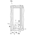
図1〜図7は、本発明に係る液晶表示パネル及びその製造方法の実施形態1を示している。具体的に、図1は、本実施形態の液晶表示パネル50の断面図である。また、図2は、液晶表示パネル50を構成するTFTアレイ基板30aの各副画素Pの平面図であり、図3は、図2中のIII−III線に沿ったTFTアレイ基板30aの断面図である。さらに、図4は、TFTアレイ基板30aの各副画素Pに設けられた接続領域R及びその近傍を拡大した平面図であり、図5は、図4中のV−V線に沿ったTFTアレイ基板30aの断面図である。Embodiment 1 of the Invention
1 to 7 show Embodiment 1 of a liquid crystal display panel and a manufacturing method thereof according to the present invention. Specifically, FIG. 1 is a cross-sectional view of the liquid
液晶表示パネル50は、図1に示すように、互いに対向するように設けられたTFTアレイ基板30a及び対向基板40と、TFTアレイ基板30a及び対向基板40の間に設けられた液晶層45と、TFTアレイ基板30a及び対向基板40を互いに接着すると共に、TFTアレイ基板30a及び対向基板40の間に液晶層45を封入するために枠状に設けられたシール材46とを備えている。ここで、液晶表示パネル50では、図1に示すように、対向基板40から突出するTFTアレイ基板30aの表面に端子領域Tが規定さえ、シール材46の内側に表示領域Dが規定されている。そして、表示領域Dでは、複数の副画素P(図2参照)がマトリクス状に配列されている。
As shown in FIG. 1, the liquid
TFTアレイ基板30aは、図2及び図3に示すように、透明基板10と、透明基板10上に互いに平行に延びるように設けられた複数のゲート線11と、各ゲート線11を覆うように設けられたゲート絶縁膜12と、ゲート絶縁膜12上に各ゲート線11と直交する方向に互いに平行に延びるように設けられた複数のソース線14と、各ゲート線11及び各ソース線14の交差部分毎、すなわち、各副画素P毎にそれぞれ設けられた複数のTFT5と、各TFT5及び各ソース線14を覆うように設けられた層間絶縁膜17と、層間絶縁膜17上に設けられた容量電極18aと、容量電極18aを覆うように設けられた容量絶縁膜19と、容量絶縁膜19上にマトリクス状に設けられ、各TFT5にそれぞれ接続された複数の画素電極20aと、各画素電極20aを覆うように設けられた配向膜(不図示)とを備えている。
As shown in FIGS. 2 and 3, the
TFT5は、図2及び図3に示すように、透明基板10上に設けられたゲート電極11aと、ゲート電極11aを覆うように設けられたゲート絶縁膜12と、ゲート絶縁膜12上にゲート電極11aに重なるように島状に設けられた半導体層13と、半導体層13上に互いに離間するように設けられたソース電極14a及びドレイン電極14bとを備えている。
2 and 3, the
ゲート電極11aは、図2に示すように、各ゲート線11が各副画素P毎に側方に突出した部分である。なお、本実施形態では、各ゲート線11の側方に突出した部分からなるゲート電極11aを例示したが、このゲート電極は、線状に延びるゲート線11の一部分であってもよい。
As shown in FIG. 2, the
半導体層13は、例えば、チャネル領域を有する真性アモルファスシリコン層(不図示)と、チャネル領域が露出するように真性アモルファスシリコン層上に設けられ、ソース電極14a及びドレイン電極14bにそれぞれ接続されたn+アモルファスシリコン層(不図示)とを備えている。なお、本実施形態では、半導体層13として、アモルファスシリコンを例示したが、半導体層13は、例えば、ポリシリコンやIn−Ga−Zn−O系などの酸化物半導体であってもよい。The
ソース電極14aは、図2に示すように、各ソース線14が各副画素P毎に側方に突出した部分である。なお、本実施形態では、各ソース線14の側方に突出した部分からなるソース電極14aを例示したが、このソース電極は、線状に延びるソース線14の一部分であってもよい。
As shown in FIG. 2, the
ドレイン電極14bは、図2及び図3に示すように、容量電極18aと絶縁状態で、すなわち、容量電極18aを覆う容量絶縁膜19に形成されたコンタクトホール19cを介して、画素電極20aに接続されている。
As shown in FIGS. 2 and 3, the
容量電極18aは、図3〜図5に示すように、全ての副画素Pにわたって一体に形成され、各副画素P毎に、ドレイン電極14bと画素電極20aとの接続部分で開口部18cを有している。そして、容量電極18aは、図3及び図5に示すように、容量絶縁膜19を介して、画素電極20aに対向することにより、各副画素P毎に補助容量6を構成している。また、容量電極18aは、図4に示すように、後述する有機絶縁膜16の開口部16cの図中左中部に突出している。
As shown in FIGS. 3 to 5, the
層間絶縁膜17は、図3及び図5に示すように、透明基板10側に設けられた無機絶縁膜15と、無機絶縁膜15に積層された有機絶縁膜16とを備えている。ここで、有機絶縁膜16は、図3〜図5に示すように、ドレイン電極14bと画素電極20aとの接続部分において開口部16cを有し、開口部16cでは、無機絶縁膜15が有機絶縁膜16から露出している。そして、有機絶縁膜16の開口部16cでは、図4及び図5に示すように、ドレイン電極14b、及び容量電極18aの突出部分が無機絶縁膜15を介して互いに重なることにより、接続領域R(図4中のハッチング部分参照)が構成されている。また、接続領域Rでは、図5に示すように、画素電極20a(最上層)/容量絶縁膜19/容量電極18a/無機絶縁膜15/ドレイン電極14b/ゲート絶縁膜12/透明基板10(最下層)の積層構造を有している。なお、図4では、図中全面に配置する画素電極(20a)が省略されている。
As shown in FIGS. 3 and 5, the
対向基板40は、例えば、透明基板(不図示)と、透明基板上に格子状に設けられたブラックマトリクス(不図示)と、ブラックマトリクスの各格子間にそれぞれ設けられた赤色層、緑色層及び青色層などの複数の着色層(不図示)と、ブラックマトリクス、各着色層を覆うように設けられた共通電極(不図示)と、共通電極上に柱状に設けられた複数のフォトスペーサ(不図示)と、共通電極及び各フォトスペーサを覆うように設けられた配向膜(不図示)とを備えている。
The
液晶層45は、電気光学特性を有するネマチックの液晶材料などにより構成されている。
The
上記構成の液晶表示パネル50は、TFTアレイ基板30a上の各画素電極20aと対向基板40上の共通電極との間に配置する液晶層45に各副画素P毎に所定の電圧を印加して、液晶層45の配向状態を変えることにより、各副画素Pにパネル内を透過する光の透過率を調整して、画像を表示するように構成されている。
The liquid
次に、本実施形態の液晶表示パネル50aの製造方法について、図6及び図7を用いて説明する。ここで、本実施形態の液晶表示パネル50aの製造方法は、TFTアレイ基板製造工程、対向基板製造工程、液晶注入工程、検出工程及び修正工程を備える。なお、図6は、修正工程における液晶表示パネル50の断面図であり、図7は、図6の液晶表示パネル50に対して、修正工程を行った後の液晶表示パネル50aの断面図である。
Next, the manufacturing method of the liquid
<TFTアレイ基板製造工程>
まず、ガラス基板やプラスチック基板などの透明基板10の基板全体に、例えば、スパッタリング法により、モリブデン膜(厚さ150nm程度)などを成膜した後に、そのモリブデン膜に対して、フォトリソグラフィ、エッチング及びレジストの剥離洗浄を行うことにより、ゲート線11及びゲート電極11aを形成する。なお、本実施形態では、モリブデン膜を用いてゲート線11及びゲート電極11aを形成する方法を例示したが、例えば、アルミニウム膜、タングステン膜、タンタル膜、クロム膜、チタン膜、銅膜などの金属膜、その合金膜や金属窒化膜、又はそれらの積層膜を用いて、ゲート線11及びゲート電極11aを形成してもよい。<TFT array substrate manufacturing process>
First, a molybdenum film (thickness of about 150 nm) or the like is formed on the entire
続いて、ゲート線11及びゲート電極11aが形成された基板全体に、例えば、プラズマCVD(Chemical Vapor Deposition)法により、窒化シリコン膜(厚さ100nm〜600nm程度)を成膜して、ゲート絶縁膜12を形成する。なお、本実施形態では、窒化シリコン膜を用いて、ゲート絶縁膜12を形成する方法を例示したが、例えば、酸化シリコン膜(SiOx)、酸化窒化シリコン膜(SiOxNy、x>y)、窒化酸化シリコン膜(SiNxOy、x>y)などの単層膜、又はそれらの積層膜を用いて、ゲート絶縁膜12を形成してもよい。
Subsequently, a silicon nitride film (having a thickness of about 100 nm to 600 nm) is formed on the entire substrate on which the
そして、ゲート絶縁膜12が形成された基板全体に、例えば、プラズマCVD法により、真性アモルファスシリコン膜(厚さ100nm程度)及びリンがドープされたn+アモルファスシリコン膜(厚さ50nm程度)を順に成膜した後に、真性アモルファスシリコン膜及びn+アモルファスシリコン膜の積層膜に対して、フォトリソグラフィ、エッチング及びレジストの剥離洗浄を行うことにより、半導体層形成部(13)を形成する。Then, an intrinsic amorphous silicon film (with a thickness of about 100 nm) and an n + amorphous silicon film (with a thickness of about 50 nm) doped with phosphorus are sequentially applied to the entire substrate on which the
さらに、半導体層形成部(13)が形成された基板全体に、例えば、スパッタリング法により、チタン膜(厚さ20nm〜150nm程度)及びアルミニウム膜(厚さ50nm〜400nm程度)などを順に成膜した後に、その金属積層膜に対して、フォトリソグラフィ、エッチング及びレジストの剥離洗浄を行うことにより、ソース線14、ソース電極14a及びドレイン電極14bを形成する。なお、本実施形態では、チタン膜及びアルミニウム膜の金属積層膜を用いて、ソース線14、ソース電極14a及びドレイン電極14bを形成する方法を例示したが、例えば、アルミニウム膜、タングステン膜、モリブデン膜、タンタル膜、クロム膜、チタン膜、銅膜などの金属膜、その合金膜や金属窒化膜、又はそれらの積層膜を用いて、ソース線14、ソース電極14a及びドレイン電極14bを形成してもよい。
Further, a titanium film (thickness of about 20 nm to 150 nm), an aluminum film (thickness of about 50 nm to 400 nm), and the like are sequentially formed on the entire substrate on which the semiconductor layer forming portion (13) is formed by, for example, sputtering. Later, the
続いて、ソース電極14a及びドレイン電極14bをマスクとして、上記半導体層形成部のn+アモルファスシリコン膜をエッチングすることにより、チャネル領域を形成して、半導体層13及びそれを備えたTFT5を形成する。Subsequently, by using the
そして、TFT5が形成された基板全体に、例えば、プラズマCVD法により、窒化シリコン膜、酸化シリコン膜、窒化酸化シリコン膜などの無機絶縁膜(15)を厚さ300nm程度で成膜する。
Then, an inorganic insulating film (15) such as a silicon nitride film, a silicon oxide film, or a silicon nitride oxide film is formed on the entire substrate on which the
さらに、無機絶縁膜(15)が成膜された基板全体に、例えば、スピンコート法又はスリットコート法により、感光性のアクリル樹脂などからなる感光性樹脂膜を厚さ2.0μm〜4.0μm程度に塗布した後に、その感光性樹脂膜に対して、露光、現像及びベーキングを行うことにより、開口部16cを有する有機絶縁膜16を形成する。
Further, a photosensitive resin film made of a photosensitive acrylic resin or the like is formed on the entire substrate on which the inorganic insulating film (15) is formed, for example, by spin coating or slit coating, to a thickness of 2.0 μm to 4.0 μm. After coating to the extent, the organic insulating
続いて、有機絶縁膜16が形成された基板全体に、例えば、スパッタリング法により、ITO(Indium Tin Oxide)膜などの透明導電膜を厚さ50nm〜200nm程度で成膜した後に、その透明導電膜に対して、フォトリソグラフィ、エッチング及びレジストの剥離洗浄を行うことにより、開口部18cを有する容量電極18aを形成する。
Subsequently, after forming a transparent conductive film such as an ITO (Indium Tin Oxide) film with a thickness of about 50 nm to 200 nm on the entire substrate on which the organic insulating
そして、容量電極18aが形成された基板全体に、例えば、プラズマCVD法により、窒化シリコン膜、酸化シリコン膜、窒化酸化シリコン膜などの無機絶縁膜を厚さ300nm程度で成膜した後に、その無機絶縁膜(19)及び先に成膜した無機絶縁膜(15)に対して、フォトリソグラフィ、エッチング及びレジストの剥離洗浄を行うことにより、無機絶縁膜15及び有機絶縁膜16からなる層間絶縁膜17、並びにコンタクトホール19cを有する容量絶縁膜19を形成する。
Then, an inorganic insulating film such as a silicon nitride film, a silicon oxide film, or a silicon nitride oxide film is formed on the entire substrate on which the
さらに、層間絶縁膜17及び容量絶縁膜19が形成された基板全体に、例えば、スパッタリング法により、ITO膜などの透明導電膜を厚さ50nm〜200nm程度で成膜した後に、その透明導電膜に対して、フォトリソグラフィ、エッチング及びレジストの剥離洗浄を行うことにより、画素電極20aを形成する。
Further, after forming a transparent conductive film such as an ITO film with a thickness of about 50 nm to 200 nm on the entire substrate on which the
最後に、画素電極20aが形成された基板全体に、例えば、印刷法によりポリイミドの樹脂膜を塗布した後に、その塗布膜に対して、焼成及びラビング処理を行うことにより、配向膜を形成する。
Finally, after applying a polyimide resin film to the entire substrate on which the
以上のようにして、TFTアレイ基板30aを製造することができる。
As described above, the
<対向基板製造工程>
まず、ガラス基板やプラスチック基板などの透明基板の基板全体に、例えば、スピンコート法又はスリットコート法により、黒色に着色された感光性樹脂を塗布した後に、その塗布膜に対して、露光、現像及びベーキングを行うことにより、ブラックマトリクスを厚さ1.0μm程度に形成する。<Opposite substrate manufacturing process>
First, a black colored photosensitive resin is applied to the entire transparent substrate such as a glass substrate or a plastic substrate by, for example, a spin coating method or a slit coating method, and then the coating film is exposed and developed. And by baking, a black matrix is formed to a thickness of about 1.0 μm.
続いて、上記ブラックマトリクスが形成された基板全体に、例えば、スピンコート法又はスリットコート法により、例えば、赤色、緑色又は青色に着色された感光性樹脂を塗布した後に、その塗布膜に対して、露光、現像及びベーキングを行うことにより、選択した色の着色層(例えば、赤色層)を厚さ2.0μm程度に形成する。そして、他の2色についても同様な工程を繰り返して、他の2色の着色層(例えば、緑色層及び青色層)を厚さ2.0μm程度に形成する。 Subsequently, a photosensitive resin colored in red, green or blue, for example, is applied to the entire substrate on which the black matrix is formed, for example, by spin coating or slit coating, and then applied to the coating film. By performing exposure, development and baking, a colored layer (for example, a red layer) of a selected color is formed to a thickness of about 2.0 μm. The same process is repeated for the other two colors to form other two colored layers (for example, a green layer and a blue layer) with a thickness of about 2.0 μm.
そして、上記各着色層が形成された基板全体に、例えば、スパッタリング法により、ITO膜などの透明導電膜を厚さ50nm〜200nm程度で成膜することにより、共通電極を形成する。 Then, a common electrode is formed by forming a transparent conductive film such as an ITO film with a thickness of about 50 nm to 200 nm on the entire substrate on which the colored layers are formed, for example, by sputtering.
さらに、上記共通電極が形成された基板全体に、例えば、スピンコート法又はスリットコート法により、感光性のアクリル樹脂などからなる感光性樹脂膜を塗布した後に、その感光性樹脂膜に対して、露光、現像及びベーキングを行うことにより、フォトスペーサを厚さ4.0μm程度に形成する。 Furthermore, after applying a photosensitive resin film made of photosensitive acrylic resin or the like to the entire substrate on which the common electrode is formed, for example, by spin coating or slit coating, By performing exposure, development and baking, a photo spacer is formed to a thickness of about 4.0 μm.
最後に、上記フォトスペーサが形成された基板全体に、例えば、印刷法によりポリイミドの樹脂膜を塗布した後に、その塗布膜に対して、焼成及びラビング処理を行うことにより、配向膜を形成する。 Finally, after applying a polyimide resin film to the entire substrate on which the photo spacers are formed by, for example, a printing method, an alignment film is formed by baking and rubbing the applied film.
以上のようにして、対向基板40を製造することができる。
The
<液晶注入工程>
まず、例えば、上記対向基板製造工程で製造された対向基板40の表面に、UV(ultraviolet)硬化及び熱硬化の併用型樹脂などからなるシール材46を枠状に印刷した後に、シール材46の内側に液晶材料を滴下する。<Liquid crystal injection process>
First, for example, after a sealing
続いて、上記液晶材料が滴下された対向基板40と、上記TFTアレイ基板製造工程で製造されたTFTアレイ基板30aとを、減圧下で貼り合わせた後に、その貼り合わせた貼合体を大気圧に開放することにより、その貼合体の表面及び裏面を加圧する。
Subsequently, the
さらに、上記貼合体に挟持されたシール材46にUV光を照射した後に、その貼合体を加熱することによりシール材46を硬化させる。
Furthermore, after irradiating UV light to the sealing
最後に、上記シール材46を硬化させた貼合体を、例えば、ダイシングにより分断することにより、その不要な部分を除去する。
Finally, the unnecessary part is removed by dividing the bonding body which hardened the said
以上のようにして、液晶表示パネル50(検査前)を製造することができる。 As described above, the liquid crystal display panel 50 (before inspection) can be manufactured.
<検出工程>
上記製造された液晶表示パネル50において、各ゲート線11に、バイアス電圧−10V、周期16.7msec、パルス幅50μsecの+15Vのパルス電圧のゲート検査信号を入力して、全ての副画素PのTFT5をオン状態にすると共に、各ソース線14に、16.7msec毎に極性が反転する±2Vの電位のソース検査信号を入力することにより、各TFT5を介して画素電極20aにソース検査信号を入力する。そして、同時に、対向基板40の共通電極に直流で−1Vの電位の共通電極検査信号を入力することにより、TFTアレイ基板30aの各画素電極20aと対向基板40の共通電極との間に配置する液晶層45に電圧を印加して、各画素電極20aにより構成される各副画素Pが点灯状態になる。このとき、例えば、ノーマリブラックモード(電圧無印加時に黒表示)の液晶表示パネル50では、表示画面が黒表示から白表示となる。ここで、膜残りなどにより、ソース電極14a及びドレイン電極14bの間で短絡S(図2中の2点鎖線参照)が発生した副画素Pでは、TFT5のオン/オフ制御に関係せず、画素電極20aにソース検査信号が常に入力されるので、その副画素Pは、黒表示の表示画面において輝点として検出される。<Detection process>
In the manufactured liquid
<修正工程>
上記検出工程で短絡Sが検出された場合には、その検出された副画素Pにおいて、図2及び図6に示すように、ドレイン電極14bのX部にレーザー光Lを照射することにより、ドレイン電極14bをX部で切断すると共に、接続領域RのY部にレーザー光Lを照射することにより、切断されたドレイン電極14bの画素電極20aに接続された側と容量電極18aとを接続する。ここで、図7の修正工程後の液晶表示パネル50aでは、互いに接続されたドレイン電極14b及び容量電極18aの符号をそれぞれ14ba及び18aaとし、それらの間に配置する無機絶縁膜15の符号を15aとし、それらを備えたTFTアレイ基板30aの符号を30aaとしている。また、レーザー光Lは、例えば、YAG(Yttrium Aluminium Garnet)レーザーなどから、2.5μm×2.5μm程度のスポットサイズで出力されたものである。なお、接続領域Rは、その大きさが5μm×5μm程度以上あれば、接続領域Rにレーザー光を照射して、修正可能である。<Correction process>
When the short circuit S is detected in the detection step, the X pixel of the
以上のようにして、黒点化による欠陥修正が行われた液晶表示パネル50aを製造することができる。
As described above, it is possible to manufacture the liquid
以上説明したように、本実施形態の液晶表示パネル50(50a)及びその製造方法によれば、TFTアレイ基板30aにおいて、ドレイン電極14b及び容量電極18aの間の層間絶縁膜17が無機絶縁膜15及び有機絶縁膜16を順に積層して形成され、ドレイン電極14b及び容量電極18aが有機絶縁膜16から露出する無機絶縁膜15を介して互いに重なる接続領域Rを備えているので、ドレイン電極14b及び容量電極18aが互いに重なる接続領域Rには、ドレイン電極14b及び容量電極18aの間を電気的に絶縁する絶縁膜として、比較的厚い有機絶縁膜16が配置されずに、比較的薄い無機絶縁膜15だけが配置される。そのため、検出工程において、点灯検査により、ソース電極14a及びドレイン電極14bの間で短絡Sが発生した副画素Pが輝点として検出された場合には、修正工程において、その短絡Sが発生した副画素Pにおいて、ドレイン電極14bにレーザー光Lを透明基板10側から照射することにより、ドレイン電極14bの金属が層間絶縁膜17(無機絶縁膜15及び有機絶縁膜16)中を飛散して、ドレイン電極14bが切断されると共に、ドレイン電極14b及び容量電極18aが無機絶縁膜15を介して互いに重なる接続領域Rにレーザー光Lを透明基板10側から照射することにより、ドレイン電極14bの金属が比較的薄い無機絶縁膜15中を飛散して容量電極18aに容易に到達するので、切断されたドレイン電極14bの画素電極20aに接続された側と容量電極18aとを確実に接続することができる。これにより、短絡Sが発生した副画素Pでは、画素電極20aが容量電極18aの電位(例えば、接地電位)に固定されて、輝点を黒点化することができるので、液晶表示パネル50(50a)の黒点化による欠陥修正において、ドレイン電極14b(14ba)と容量電極18a(18aa)とを確実に接続することができる。
As described above, according to the liquid crystal display panel 50 (50a) of this embodiment and the manufacturing method thereof, in the
《発明の実施形態2》
図8は、本実施形態の液晶表示パネルを構成するTFTアレイ基板30bの各副画素Pに設けられた接続領域R及びその近傍を拡大した平面図である。ここで、図8では、図4と同様に、図中全面に配置する画素電極(20a)が省略されている。なお、以下の各実施形態において、図1〜図7と同じ部分については同じ符号を付して、その詳細な説明を省略する。<< Embodiment 2 of the Invention >>
FIG. 8 is an enlarged plan view of the connection region R provided in each sub-pixel P of the
上記実施形態1では、レーザー光Lを照射するY部の大部分が接続領域Rに含まれる液晶表示パネル50(50a)の製造方法を例示したが、本実施形態では、レーザー光Lを照射するY部の一部分が接続領域Rに含まれる液晶表示パネルの製造方法を例示する。 In the said Embodiment 1, although the manufacturing method of the liquid crystal display panel 50 (50a) in which most Y parts which irradiate the laser beam L are contained in the connection area | region R was illustrated, in this embodiment, the laser beam L is irradiated. A method for manufacturing a liquid crystal display panel in which a part of the Y portion is included in the connection region R will be exemplified.
本実施形態の液晶表示パネルは、互いに対向するように設けられたTFTアレイ基板30b(図8参照)及び対向基板40(図1参照)と、TFTアレイ基板30b及び対向基板40の間に設けられた液晶層45(図1参照)と、TFTアレイ基板30b及び対向基板40を互いに接着すると共に、TFTアレイ基板30b及び対向基板40の間に液晶層45を封入するために枠状に設けられたシール材46(図1参照)とを備えている。
The liquid crystal display panel of this embodiment is provided between the
TFTアレイ基板30bは、透明基板10(図3参照)と、透明基板10上に互いに平行に延びるように設けられた複数のゲート線11(図2参照)と、各ゲート線11を覆うように設けられたゲート絶縁膜12(図3参照)と、ゲート絶縁膜12上に各ゲート線11と直交する方向に互いに平行に延びるように設けられた複数のソース線14(図2参照)と、各ゲート線11及び各ソース線14の交差部分毎にそれぞれ設けられた複数のTFT5(図2及び図3参照)と、各TFT5及び各ソース線14を覆うように設けられた層間絶縁膜17(図3参照)と、層間絶縁膜17上に設けられた容量電極18b(図8参照)と、容量電極18bを覆うように設けられた容量絶縁膜19(図3参照)と、容量絶縁膜19上にマトリクス状に設けられ、各TFT5にそれぞれ接続された複数の画素電極20a(図2及び図3参照)と、各画素電極20aを覆うように設けられた配向膜(不図示)とを備えている。
The
TFTアレイ基板30bでは、図8に示すように、容量電極18bが有機絶縁膜16の開口部16cの図中左下部に突出している。そして、有機絶縁膜16の開口部16cでは、図8に示すように、ドレイン電極14b、及び容量電極18bの突出部分が無機絶縁膜15を介して互いに重なることにより、接続領域R(図中のハッチング部分参照)が構成されている。
In the
本実施形態のTFTアレイ基板30b及びそれを備えた液晶表示パネルは、上記実施形態1のTFTアレイ基板製造工程において、容量電極18aのパターン形状を変更すれば、製造することができる。そして、製造されたTFTアレイ基板30bを備えた液晶表示パネルに対して、上記実施形態1と同様に、検出工程を行い、短絡Sが検出された場合には、修正工程を行うことになる。具体的に、その修正工程では、短絡Sが検出された副画素Pにおいて、上記実施形態1と同様に、図2に示すように、ドレイン電極14bのX部にレーザー光Lを照射することにより、ドレイン電極14bをX部で切断すると共に、図8に示すように、接続領域Rの図中右上部及びそれに隣接する接続領域Rの外部を含むY部にレーザー光Lを照射することにより、切断されたドレイン電極14bの画素電極20aに接続された側と容量電極18bとを接続する。
The
以上説明したように、本実施形態のTFTアレイ基板30bを備えた液晶表示パネル及びその製造方法によれば、上記実施形態1と同様に、TFTアレイ基板30bにおいて、ドレイン電極14b及び容量電極18bの間の層間絶縁膜17が無機絶縁膜15及び有機絶縁膜16を順に積層して形成され、ドレイン電極14b及び容量電極18bが有機絶縁膜16から露出する無機絶縁膜15を介して互いに重なる接続領域Rを備えているので、液晶表示パネルの黒点化による欠陥修正において、ドレイン電極14bと容量電極18bとを確実に接続することができる。
As described above, according to the liquid crystal display panel including the
また、本実施形態のTFTアレイ基板30bを備えた液晶表示パネル及びその製造方法によれば、修正工程では、接続領域Rの端部及びそれに隣接する接続領域Rの外部にレーザー光Lを照射することにより、レーザー光Lの照射が接続領域Rだけに集中しないので、ドレイン電極14bの金属の過度の飛散を抑制することができ、ドレイン電極14bと容量電極18bとをいっそう確実に接続することができる。
Further, according to the liquid crystal display panel including the
《発明の実施形態3》
図9は、本実施形態の液晶表示パネルを構成するTFTアレイ基板30cの各副画素Pに設けられた接続領域R及びその近傍を拡大した平面図であり、図10は、図9中のX−X線に沿ったTFTアレイ基板30cの断面図である。<< Embodiment 3 of the Invention >>
FIG. 9 is an enlarged plan view of the connection region R provided in each subpixel P of the
上記各実施形態では、接続領域Rに画素電極20aが重なっているTFTアレイ基板30a及び30bを例示したが、本実施形態では、接続領域Rに画素電極20bが重なっていないTFTアレイ基板30cを例示する。
In each of the above embodiments, the
本実施形態の液晶表示パネルは、互いに対向するように設けられたTFTアレイ基板30c(図9及び図10参照)及び対向基板40(図1参照)と、TFTアレイ基板30c及び対向基板40の間に設けられた液晶層45(図1参照)と、TFTアレイ基板30c及び対向基板40を互いに接着すると共に、TFTアレイ基板30c及び対向基板40の間に液晶層45を封入するために枠状に設けられたシール材46(図1参照)とを備えている。
The liquid crystal display panel of this embodiment includes a
TFTアレイ基板30cは、図9及び図10に示すように、透明基板10と、透明基板10上に互いに平行に延びるように設けられた複数のゲート線11(図2参照)と、各ゲート線11を覆うように設けられたゲート絶縁膜12と、ゲート絶縁膜12上に各ゲート線11と直交する方向に互いに平行に延びるように設けられた複数のソース線14(図2参照)と、各ゲート線11及び各ソース線14の交差部分毎にそれぞれ設けられた複数のTFT5(図2及び図3参照)と、各TFT5及び各ソース線14を覆うように設けられた層間絶縁膜17と、層間絶縁膜17上に設けられた容量電極18bと、容量電極18bを覆うように設けられた容量絶縁膜19と、容量絶縁膜19上にマトリクス状に設けられ、各TFT5にそれぞれ接続された複数の画素電極20bと、各画素電極20bを覆うように設けられた配向膜(不図示)とを備えている。
As shown in FIGS. 9 and 10, the
TFTアレイ基板30cでは、図9に示すように、容量電極18bが有機絶縁膜16の開口部16cの図中左下部に突出している。そして、有機絶縁膜16の開口部16cでは、図9及び図10に示すように、ドレイン電極14b、及び容量電極18bの突出部分が無機絶縁膜15を介して互いに重なることにより、接続領域R(図9中のハッチング部分参照)が構成されている。
In the
また、TFTアレイ基板30cでは、図9及び図10に示すように、接続領域Rに重なるように、画素電極20bの開口部20cが設けられている。ここで、画素電極20bの開口部20cは、液晶層45の配向を規制するための構造体として機能するよう構成されている。
Further, in the
本実施形態のTFTアレイ基板30c及びそれを備えた液晶表示パネルは、上記実施形態1のTFTアレイ基板製造工程において、容量電極18a及び画素電極20aのパターン形状を変更すれば、製造することができる。そして、製造されたTFTアレイ基板30cを備えた液晶表示パネルに対して、上記実施形態1と同様に、検出工程を行い、短絡Sが検出された場合には、修正工程を行うことになる。具体的に、その修正工程では、短絡Sが検出された副画素Pにおいて、上記実施形態1と同様に、図2に示すように、ドレイン電極14bのX部にレーザー光Lを照射することにより、ドレイン電極14bをX部で切断すると共に、図9に示すように、接続領域Rの図中右上部及びそれに隣接する接続領域Rの外部を含むY部にレーザー光Lを照射することにより、切断されたドレイン電極14bの画素電極20bに接続された側と容量電極18bとを接続する。
The
以上説明したように、本実施形態のTFTアレイ基板30cを備えた液晶表示パネル及びその製造方法によれば、上記実施形態1及び2と同様に、TFTアレイ基板30cにおいて、ドレイン電極14b及び容量電極18bの間の層間絶縁膜17が無機絶縁膜15及び有機絶縁膜16を順に積層して形成され、ドレイン電極14b及び容量電極18bが有機絶縁膜16から露出する無機絶縁膜15を介して互いに重なる接続領域Rを備えているので、液晶表示パネルの黒点化による欠陥修正において、ドレイン電極14bと容量電極18bとを確実に接続することができる。
As described above, according to the liquid crystal display panel including the
また、本実施形態のTFTアレイ基板30cを備えた液晶表示パネル及びその製造方法によれば、修正工程では、接続領域Rの端部及びそれに隣接する接続領域Rの外部にレーザー光Lを照射することにより、レーザー光Lの照射が接続領域Rだけに集中しないので、ドレイン電極14bの金属の過度の飛散を抑制することができ、ドレイン電極14bと容量電極18bとをいっそう確実に接続することができる。
Further, according to the liquid crystal display panel including the
また、本実施形態のTFTアレイ基板30cを備えた液晶表示パネル及びその製造方法によれば、各画素電極20bには、液晶層45の配向を規制するための構造体として、接続領域Rに重なるように開口部20cが設けられているので、接続領域Rに対するレーザー光Lの照射による画素電極20bの損傷を抑制することができる。
In addition, according to the liquid crystal display panel including the
《発明の実施形態4》
図11は、本発明に係るTFTアレイ基板及びその製造方法の実施形態を示している。具体的に、図11は、本実施形態の修正工程におけるTFTアレイ基板30aの断面図である。<< Embodiment 4 of the Invention >>
FIG. 11 shows an embodiment of a TFT array substrate and a manufacturing method thereof according to the present invention. Specifically, FIG. 11 is a cross-sectional view of the
上記各実施形態では、パネル状態で検出工程及び修正工程を行う液晶表示パネル及びその製造方法を例示したが、本実施形態では、基板状態で検出工程及び修正工程を行うTFTアレイ基板30a及びその製造方法を例示する。
In each of the above embodiments, the liquid crystal display panel that performs the detection process and the correction process in the panel state and the manufacturing method thereof are exemplified. However, in this embodiment, the
本実施形態のTFTアレイ基板30aは、上記実施形態1のTFTアレイ基板30aと同一であるが、上記実施形態2のTFTアレイ基板30bや上記実施形態3のTFTアレイ基板30cであってもよい。
The
本実施形態のTFTアレイ基板30aは、例えば、CCD(Charge Coupled Device)カメラによる光学的検査や電荷検出法による検査により、ソース電極14a及びドレイン電極14bの間で短絡Sが発生した副画素Pが検出することにより、検出工程を行い、短絡Sが検出された場合には、修正工程を行うことになる。具体的に、その修正工程では、短絡Sが検出された副画素Pにおいて、ドレイン電極14bのX部(図2参照)にレーザー光Lを照射することにより、ドレイン電極14bをX部で切断すると共に、図11に示すように、接続領域RのY部(図4参照)にレーザー光Lを照射することにより、切断されたドレイン電極14bの画素電極20aに接続された側と容量電極18aとを接続する(図7中のTFTアレイ基板30aa参照)。
In the
以上説明したように、本実施形態のTFTアレイ基板30a及びその製造方法によれば、ドレイン電極14b及び容量電極18aの間の層間絶縁膜17が無機絶縁膜15及び有機絶縁膜16を順に積層して形成され、ドレイン電極14b及び容量電極18aが有機絶縁膜16から露出する無機絶縁膜15を介して互いに重なる接続領域Rを備えているので、ドレイン電極14b及び容量電極18aが互いに重なる接続領域Rには、ドレイン電極14b及び容量電極18aの間を電気的に絶縁する絶縁膜として、比較的厚い有機絶縁膜16が配置されずに、比較的薄い無機絶縁膜15だけが配置される。そのため、検出工程において、光学的検査や電荷検出法による検査により、ソース電極14a及びドレイン電極14bの間で短絡Sが発生した副画素Pが検出された場合には、修正工程において、その短絡Sが発生した副画素Pにおいて、ドレイン電極14bにレーザー光Lを透明基板10側から照射することにより、ドレイン電極14bの金属が層間絶縁膜17(無機絶縁膜15及び有機絶縁膜16)中を飛散して、ドレイン電極14bが切断されると共に、ドレイン電極14b及び容量電極18aが無機絶縁膜15を介して互いに重なる接続領域Rにレーザー光Lを透明基板10側から照射することにより、ドレイン電極14bの金属が比較的薄い無機絶縁膜15中を飛散して容量電極18aに容易に到達するので、切断されたドレイン電極14bの画素電極20aに接続された側と容量電極18aとを確実に接続することができる。これにより、短絡Sが発生した副画素Pでは、画素電極20aが容量電極18aの電位(例えば、接地電位)に固定されて、黒点化されるので、TFTアレイ基板30aの黒点化による欠陥修正において、ドレイン電極14bと容量電極18aとを確実に接続することができる。
As described above, according to the
なお、上記各実施形態では、ドレイン電極14bを切断する修正方法を例示したが、ソース電極14aが切断可能な構造であれば、ドレイン電極14bを切断する代わりに、ソース電極14aをその基部で切断してもよい。
In each of the above embodiments, the correction method for cutting the
また、上記各実施形態では、スイッチング素子として、TFTを例示したが、本発明は、MOSFET(Metal Oxide Semiconductor Field Effect Transistor)などの他の3端子のスイッチング素子にも適用することができる。 In each of the above embodiments, the TFT is exemplified as the switching element. However, the present invention can also be applied to other three-terminal switching elements such as a MOSFET (Metal Oxide Semiconductor Field Effect Transistor).
また、上記各実施形態では、各画素が3つの副画素(赤、緑及び青)を有する液晶表示パネルを例示したが、本発明は、各画素が4つ以上の副画素(例えば、赤、緑、青及び白や赤、緑、青及び黄など)を有する液晶表示パネルにも適用することができる。 In each of the above embodiments, a liquid crystal display panel in which each pixel has three subpixels (red, green, and blue) is illustrated. However, in the present invention, each pixel has four or more subpixels (for example, red, green, and blue). The present invention can also be applied to liquid crystal display panels having green, blue, white, red, green, blue, yellow, and the like.
また、上記各実施形態では、複数の副画素がマトリクス状に配列されたアレイ基板及びそれを備えた液晶表示パネルを例示したが、本発明は、複数の副画素がデルタ状に配列されたアレイ基板及びそれを備えた液晶表示パネルにも適用することができる。 In each of the above embodiments, an array substrate in which a plurality of subpixels are arranged in a matrix and a liquid crystal display panel including the same are exemplified. However, the present invention is an array in which a plurality of subpixels are arranged in a delta shape. The present invention can also be applied to a substrate and a liquid crystal display panel including the substrate.
また、上記各実施形態では、画素電極に接続されたTFTの電極をドレイン電極としたTFTアレイ基板を例示したが、本発明は、画素電極に接続されたTFTの電極をソース電極と呼ぶTFTアレイ基板にも適用することができる。 In each of the above embodiments, the TFT array substrate using the TFT electrode connected to the pixel electrode as the drain electrode has been exemplified. However, in the present invention, the TFT array connected to the pixel electrode is referred to as a source electrode. It can also be applied to a substrate.
以上説明したように、本発明は、黒点化による欠陥修正において、ドレイン電極と容量電極とを確実に接続するので、補助容量を有する表示パネルについて有用である。 As described above, the present invention is useful for a display panel having an auxiliary capacitor because the drain electrode and the capacitor electrode are reliably connected in defect correction by blackening.
L レーザー光
P 副画素
R 接続領域
S 短絡
5 TFT(スイッチング素子)
6 補助容量
10 透明基板
12 ゲート絶縁膜
14a ソース電極
14b ドレイン電極
15,15a 無機絶縁膜
16 有機絶縁膜
17 層間絶縁膜
18a,18b 容量電極
19 容量絶縁膜
20a,20b 画素電極
20c 開口部
30a,30aa,30b,30c TFTアレイ基板
40 対向基板
45 液晶層
50,50a 液晶表示パネルL Laser light P Subpixel R Connection area
6
Claims (15)
互いに対向するように設けられたアレイ基板及び対向基板と、
上記アレイ基板及び対向基板の間に設けられた液晶層とを備え、
上記アレイ基板が、
透明基板に上記各副画素毎にそれぞれ設けられ、各々、互いに離間するように配置されたソース電極及びドレイン電極を有する複数のスイッチング素子と、
上記各スイッチング素子を覆うように設けられ、無機絶縁膜及び有機絶縁膜が順に積層された層間絶縁膜と、
上記層間絶縁膜上に設けられた容量電極と、
上記容量電極を覆うように設けられた容量絶縁膜と、
上記容量絶縁膜上に設けられ、上記容量電極に対向して上記各副画素毎に補助容量を構成し、該容量電極と絶縁状態で上記各スイッチング素子のドレイン電極にそれぞれ接続された複数の画素電極とを備えた液晶表示パネルであって、
上記アレイ基板には、上記ドレイン電極及び容量電極が上記有機絶縁膜から露出する上記無機絶縁膜を介して互いに重なる接続領域が設けられていることを特徴とする液晶表示パネル。 A plurality of subpixels;
An array substrate and a counter substrate provided to face each other;
A liquid crystal layer provided between the array substrate and the counter substrate,
The array substrate is
A plurality of switching elements provided for each of the sub-pixels on the transparent substrate, each having a source electrode and a drain electrode disposed so as to be separated from each other;
An interlayer insulating film that is provided so as to cover each of the switching elements, and in which an inorganic insulating film and an organic insulating film are sequentially stacked;
A capacitor electrode provided on the interlayer insulating film;
A capacitive insulating film provided to cover the capacitive electrode;
A plurality of pixels provided on the capacitor insulating film, configured as auxiliary capacitors for each of the sub-pixels facing the capacitor electrode, and connected to the drain electrodes of the switching elements in an insulated state from the capacitor electrode. A liquid crystal display panel comprising electrodes,
The liquid crystal display panel, wherein the array substrate is provided with a connection region in which the drain electrode and the capacitor electrode overlap with each other through the inorganic insulating film exposed from the organic insulating film.
上記各画素電極には、上記接続領域に重なるように開口部が設けられていることを特徴とする液晶表示パネル。 The liquid crystal display panel according to claim 1,
Each of the pixel electrodes is provided with an opening so as to overlap the connection region.
上記アレイ基板の上記接続領域では、上記透明基板上にゲート絶縁膜、上記ドレイン電極、無機絶縁膜、容量電極、容量絶縁膜及び各画素電極が順に積層されていることを特徴とする液晶表示パネル。 The liquid crystal display panel according to claim 1,
In the connection region of the array substrate, a gate insulating film, the drain electrode, an inorganic insulating film, a capacitor electrode, a capacitor insulating film, and each pixel electrode are sequentially stacked on the transparent substrate. .
上記各スイッチング素子は、酸化物半導体により構成された半導体層を備えた薄膜トランジスタであることを特徴とする液晶表示パネル。Each of the switching elements is a thin film transistor provided with a semiconductor layer made of an oxide semiconductor.
上記酸化物半導体は、In−Ga−Zn−O系であることを特徴とする液晶表示パネル。The oxide semiconductor is an In—Ga—Zn—O-based liquid crystal display panel.
互いに対向するように設けられたアレイ基板及び対向基板と、
上記アレイ基板及び対向基板の間に設けられた液晶層とを備え、
上記アレイ基板が、
透明基板に上記各副画素毎にそれぞれ設けられ、各々、互いに離間するように配置されたソース電極及びドレイン電極を有する複数のスイッチング素子と、
上記各スイッチング素子を覆うように設けられ、無機絶縁膜及び有機絶縁膜が順に積層された層間絶縁膜と、
上記層間絶縁膜上に設けられた容量電極と、
上記容量電極を覆うように設けられた容量絶縁膜と、
上記容量絶縁膜上に設けられ、上記容量電極に対向して上記各副画素毎に補助容量を構成し、該容量電極と絶縁状態で上記各スイッチング素子のドレイン電極にそれぞれ接続された複数の画素電極とを備え、
上記アレイ基板には、上記ドレイン電極及び容量電極が上記有機絶縁膜から露出する上記無機絶縁膜を介して互いに重なる接続領域が設けられた液晶表示パネルを製造する方法であって、
上記複数の副画素において、上記ソース電極及びドレイン電極の間で短絡が発生した副画素を検出する検出工程と、
上記検出工程で短絡が検出された副画素において、上記ドレイン電極にレーザー光を上記透明基板側から照射して該ドレイン電極を切断すると共に、上記接続領域にレーザー光を上記透明基板側から照射して、該切断されたドレイン電極の上記各画素電極に接続された側と上記容量電極とを接続する修正工程とを備えることを特徴とする液晶表示パネルの製造方法。 A plurality of subpixels;
An array substrate and a counter substrate provided to face each other;
A liquid crystal layer provided between the array substrate and the counter substrate,
The array substrate is
A plurality of switching elements provided for each of the sub-pixels on the transparent substrate, each having a source electrode and a drain electrode disposed so as to be separated from each other;
An interlayer insulating film that is provided so as to cover each of the switching elements, and in which an inorganic insulating film and an organic insulating film are sequentially stacked;
A capacitor electrode provided on the interlayer insulating film;
A capacitive insulating film provided to cover the capacitive electrode;
A plurality of pixels provided on the capacitor insulating film, configured as auxiliary capacitors for each of the sub-pixels facing the capacitor electrode, and connected to the drain electrodes of the switching elements in an insulated state from the capacitor electrode. With electrodes,
The array substrate is a method for manufacturing a liquid crystal display panel in which the drain electrode and the capacitor electrode are provided with connection regions overlapping each other through the inorganic insulating film exposed from the organic insulating film,
In the plurality of subpixels, a detection step of detecting a subpixel in which a short circuit has occurred between the source electrode and the drain electrode;
In the subpixel in which a short circuit is detected in the detection step, the drain electrode is irradiated with laser light from the transparent substrate side to cut the drain electrode, and the connection region is irradiated with laser light from the transparent substrate side. And a correcting step for connecting the side of the cut drain electrode connected to each pixel electrode and the capacitor electrode.
上記修正工程では、上記接続領域の端部及び該端部に隣接する該接続領域の外部に上記レーザー光を照射することを特徴とする液晶表示パネルの製造方法。 In the manufacturing method of the liquid crystal display panel described in Claim 6 ,
In the correcting step, the laser light is irradiated to the end of the connection region and the outside of the connection region adjacent to the end.
上記各スイッチング素子は、酸化物半導体により構成された半導体層を備えた薄膜トランジスタであることを特徴とする液晶表示パネルの製造方法。Each of the switching elements is a thin film transistor provided with a semiconductor layer made of an oxide semiconductor.
上記酸化物半導体は、In−Ga−Zn−O系であることを特徴とする液晶表示パネルの製造方法。The method for manufacturing a liquid crystal display panel, wherein the oxide semiconductor is In—Ga—Zn—O-based.
透明基板に上記各副画素毎にそれぞれ設けられ、各々、互いに離間するように配置されたソース電極及びドレイン電極を有する複数のスイッチング素子と、
上記各スイッチング素子を覆うように設けられ、無機絶縁膜及び有機絶縁膜が順に積層された層間絶縁膜と、
上記層間絶縁膜上に設けられた容量電極と、
上記容量電極を覆うように設けられた容量絶縁膜と、
上記容量絶縁膜上に設けられ、上記容量電極に対向して上記各副画素毎に補助容量を構成し、該容量電極と絶縁状態で上記各スイッチング素子のドレイン電極にそれぞれ接続された複数の画素電極とを備えたアレイ基板であって、
上記ドレイン電極及び容量電極が上記有機絶縁膜から露出する上記無機絶縁膜を介して互いに重なる接続領域を備えていることを特徴とするアレイ基板。 A plurality of subpixels;
A plurality of switching elements provided for each of the sub-pixels on the transparent substrate, each having a source electrode and a drain electrode disposed so as to be separated from each other;
An interlayer insulating film that is provided so as to cover each of the switching elements, and in which an inorganic insulating film and an organic insulating film are sequentially stacked;
A capacitor electrode provided on the interlayer insulating film;
A capacitive insulating film provided to cover the capacitive electrode;
A plurality of pixels provided on the capacitor insulating film, configured as auxiliary capacitors for each of the sub-pixels facing the capacitor electrode, and connected to the drain electrodes of the switching elements in an insulated state from the capacitor electrode. An array substrate comprising electrodes,
An array substrate comprising a connection region in which the drain electrode and the capacitor electrode overlap with each other through the inorganic insulating film exposed from the organic insulating film.
上記各スイッチング素子は、酸化物半導体により構成された半導体層を備えた薄膜トランジスタであることを特徴とするアレイ基板。Each of the switching elements is a thin film transistor provided with a semiconductor layer made of an oxide semiconductor.
上記酸化物半導体は、In−Ga−Zn−O系であることを特徴とするアレイ基板。The oxide substrate is an In—Ga—Zn—O-based array substrate.
透明基板に上記各副画素毎にそれぞれ設けられ、各々、互いに離間するように配置されたソース電極及びドレイン電極を有する複数のスイッチング素子と、
上記各スイッチング素子を覆うように設けられ、無機絶縁膜及び有機絶縁膜が順に積層された層間絶縁膜と、
上記層間絶縁膜上に設けられた容量電極と、
上記容量電極を覆うように設けられた容量絶縁膜と、
上記容量絶縁膜上に設けられ、上記容量電極に対向して上記各副画素毎に補助容量を構成し、該容量電極と絶縁状態で上記各スイッチング素子のドレイン電極にそれぞれ接続された複数の画素電極と、
上記ドレイン電極及び容量電極が上記有機絶縁膜から露出する上記無機絶縁膜を介して互いに重なるように設けられた接続領域とを備えたアレイ基板を製造する方法であって、
上記複数の副画素において、上記ソース電極及びドレイン電極の間で短絡が発生した副画素を検出する検出工程と、
上記検出工程で短絡が検出された副画素において、上記ドレイン電極にレーザー光を上記透明基板側から照射して該ドレイン電極を切断すると共に、上記接続領域にレーザー光を上記透明基板側から照射して、該切断されたドレイン電極の上記各画素電極に接続された側と上記容量電極とを接続する修正工程とを備えることを特徴とするアレイ基板の製造方法。 A plurality of subpixels;
A plurality of switching elements provided for each of the sub-pixels on the transparent substrate, each having a source electrode and a drain electrode disposed so as to be separated from each other;
An interlayer insulating film that is provided so as to cover each of the switching elements, and in which an inorganic insulating film and an organic insulating film are sequentially stacked;
A capacitor electrode provided on the interlayer insulating film;
A capacitive insulating film provided to cover the capacitive electrode;
A plurality of pixels provided on the capacitor insulating film, configured as auxiliary capacitors for each of the sub-pixels facing the capacitor electrode, and connected to the drain electrodes of the switching elements in an insulated state from the capacitor electrode. Electrodes,
A method of manufacturing an array substrate including a connection region provided so that the drain electrode and the capacitor electrode overlap each other via the inorganic insulating film exposed from the organic insulating film,
In the plurality of subpixels, a detection step of detecting a subpixel in which a short circuit has occurred between the source electrode and the drain electrode;
In the subpixel in which a short circuit is detected in the detection step, the drain electrode is irradiated with laser light from the transparent substrate side to cut the drain electrode, and the connection region is irradiated with laser light from the transparent substrate side. And a correction step of connecting the capacitor electrode to the side of the cut drain electrode connected to each of the pixel electrodes.
上記各スイッチング素子は、酸化物半導体により構成された半導体層を備えた薄膜トランジスタであることを特徴とするアレイ基板の製造方法。Each of the switching elements is a thin film transistor provided with a semiconductor layer made of an oxide semiconductor.
上記酸化物半導体は、In−Ga−Zn−O系であることを特徴とするアレイ基板の製造方法。The method for manufacturing an array substrate, wherein the oxide semiconductor is In—Ga—Zn—O-based.
Priority Applications (1)
| Application Number | Priority Date | Filing Date | Title |
|---|---|---|---|
| JP2012555726A JP5243664B2 (en) | 2011-01-31 | 2012-01-24 | Liquid crystal display panel and manufacturing method thereof, and array substrate and manufacturing method thereof |
Applications Claiming Priority (4)
| Application Number | Priority Date | Filing Date | Title |
|---|---|---|---|
| JP2011018806 | 2011-01-31 | ||
| JP2011018806 | 2011-01-31 | ||
| PCT/JP2012/000420 WO2012105180A1 (en) | 2011-01-31 | 2012-01-24 | Liquid crystal display panel, production method for same, and array substrate and production method for same |
| JP2012555726A JP5243664B2 (en) | 2011-01-31 | 2012-01-24 | Liquid crystal display panel and manufacturing method thereof, and array substrate and manufacturing method thereof |
Publications (2)
| Publication Number | Publication Date |
|---|---|
| JP5243664B2 true JP5243664B2 (en) | 2013-07-24 |
| JPWO2012105180A1 JPWO2012105180A1 (en) | 2014-07-03 |
Family
ID=46602407
Family Applications (1)
| Application Number | Title | Priority Date | Filing Date |
|---|---|---|---|
| JP2012555726A Active JP5243664B2 (en) | 2011-01-31 | 2012-01-24 | Liquid crystal display panel and manufacturing method thereof, and array substrate and manufacturing method thereof |
Country Status (7)
| Country | Link |
|---|---|
| US (1) | US8629948B2 (en) |
| EP (1) | EP2672317B1 (en) |
| JP (1) | JP5243664B2 (en) |
| KR (1) | KR101311693B1 (en) |
| CN (1) | CN103229095B (en) |
| TW (1) | TWI415239B (en) |
| WO (1) | WO2012105180A1 (en) |
Families Citing this family (15)
| Publication number | Priority date | Publication date | Assignee | Title |
|---|---|---|---|---|
| KR20140118005A (en) * | 2013-03-27 | 2014-10-08 | 삼성디스플레이 주식회사 | Organic light emitting device display and manufacturing method thereof |
| WO2015071989A1 (en) * | 2013-11-14 | 2015-05-21 | 堺ディスプレイプロダクト株式会社 | Circuit board and display device |
| KR102253966B1 (en) * | 2013-12-09 | 2021-05-18 | 엘지디스플레이 주식회사 | Organic light emitting diode display device, fabricating and inspecting method thereof |
| JP6451054B2 (en) * | 2014-01-23 | 2019-01-16 | 凸版印刷株式会社 | THIN FILM TRANSISTOR ARRAY, ITS MANUFACTURING METHOD, AND IMAGE DISPLAY DEVICE |
| KR20150137218A (en) * | 2014-05-28 | 2015-12-09 | 삼성디스플레이 주식회사 | Liquid crystal display device and method for manufacturing the same |
| JP6463065B2 (en) * | 2014-10-09 | 2019-01-30 | 三菱電機株式会社 | Array substrate, liquid crystal display panel including the same, and array substrate inspection method |
| CN104730790B (en) * | 2015-03-25 | 2018-05-11 | 深圳市华星光电技术有限公司 | Liquid crystal display device, liquid crystal display and preparation method thereof and dim spot operational method |
| CN105487315A (en) * | 2016-01-19 | 2016-04-13 | 武汉华星光电技术有限公司 | TFT (thin film transistor) array substrate |
| CN105759522B (en) * | 2016-05-11 | 2019-01-22 | 深圳市华星光电技术有限公司 | The broken wire repair method of TFT substrate |
| WO2018131649A1 (en) * | 2017-01-16 | 2018-07-19 | シャープ株式会社 | Active matrix substrate, liquid crystal display panel, and method for manufacturing liquid crystal display panel |
| KR102193700B1 (en) * | 2018-07-11 | 2020-12-21 | 엘지전자 주식회사 | Display device using semiconductor light emitting device |
| JP7160334B2 (en) | 2018-11-22 | 2022-10-25 | 株式会社ジャパンディスプレイ | Display device |
| CN109728000B (en) * | 2019-01-02 | 2021-01-15 | 京东方科技集团股份有限公司 | Transparent display substrate and display panel |
| CN111430383B (en) | 2020-05-20 | 2023-04-28 | 合肥鑫晟光电科技有限公司 | Array substrate, manufacturing method thereof and display device |
| CN112349205B (en) * | 2020-10-26 | 2022-09-27 | 京东方科技集团股份有限公司 | Array substrate, maintenance method thereof and display panel |
Citations (3)
| Publication number | Priority date | Publication date | Assignee | Title |
|---|---|---|---|---|
| JPH04256362A (en) * | 1991-02-08 | 1992-09-11 | Sanyo Electric Co Ltd | Display device and its remedy method |
| JPH04324819A (en) * | 1991-04-25 | 1992-11-13 | Seiko Epson Corp | Picture element defect correcting method for active matrix displaying body and displaying body thereof |
| WO2010146747A1 (en) * | 2009-06-19 | 2010-12-23 | シャープ株式会社 | Active matrix substrate, liquid crystal panel, liquid crystal display device, liquid crystal display unit, and television receiver |
Family Cites Families (9)
| Publication number | Priority date | Publication date | Assignee | Title |
|---|---|---|---|---|
| KR970011972A (en) * | 1995-08-11 | 1997-03-29 | 쯔지 하루오 | Transmission type liquid crystal display device and manufacturing method thereof |
| JPH09179143A (en) | 1995-12-27 | 1997-07-11 | Sharp Corp | Defective picture element correcting method for liquid crystal display device |
| KR101006434B1 (en) * | 2003-06-26 | 2011-01-06 | 삼성전자주식회사 | thin film transistor array panel and method for repairing liquid crystal display including the same |
| JP4882662B2 (en) * | 2006-01-12 | 2012-02-22 | セイコーエプソン株式会社 | Electro-optical device and electronic apparatus |
| US7855757B2 (en) * | 2006-07-28 | 2010-12-21 | Samsung Electronics Co., Ltd. | Liquid crystal display, method of manufacturing the same, and method of repairing the same |
| KR101211087B1 (en) * | 2006-11-30 | 2012-12-12 | 삼성디스플레이 주식회사 | Thin film transistor substrate and display device having the same |
| US8446539B2 (en) * | 2007-03-13 | 2013-05-21 | Sharp Kabushiki Kaisha | Display panel and display apparatus |
| JP2009163214A (en) * | 2007-11-02 | 2009-07-23 | Epson Imaging Devices Corp | Liquid crystal display |
| TWI392946B (en) * | 2009-12-18 | 2013-04-11 | Au Optronics Corp | Pixel structure |
-
2012
- 2012-01-24 CN CN201280003813.5A patent/CN103229095B/en not_active Expired - Fee Related
- 2012-01-24 US US13/884,704 patent/US8629948B2/en not_active Expired - Fee Related
- 2012-01-24 EP EP20120741701 patent/EP2672317B1/en not_active Not-in-force
- 2012-01-24 JP JP2012555726A patent/JP5243664B2/en active Active
- 2012-01-24 KR KR1020137012378A patent/KR101311693B1/en not_active IP Right Cessation
- 2012-01-24 WO PCT/JP2012/000420 patent/WO2012105180A1/en active Application Filing
- 2012-01-31 TW TW101103118A patent/TWI415239B/en not_active IP Right Cessation
Patent Citations (3)
| Publication number | Priority date | Publication date | Assignee | Title |
|---|---|---|---|---|
| JPH04256362A (en) * | 1991-02-08 | 1992-09-11 | Sanyo Electric Co Ltd | Display device and its remedy method |
| JPH04324819A (en) * | 1991-04-25 | 1992-11-13 | Seiko Epson Corp | Picture element defect correcting method for active matrix displaying body and displaying body thereof |
| WO2010146747A1 (en) * | 2009-06-19 | 2010-12-23 | シャープ株式会社 | Active matrix substrate, liquid crystal panel, liquid crystal display device, liquid crystal display unit, and television receiver |
Also Published As
| Publication number | Publication date |
|---|---|
| CN103229095B (en) | 2015-11-25 |
| EP2672317A1 (en) | 2013-12-11 |
| TWI415239B (en) | 2013-11-11 |
| KR101311693B1 (en) | 2013-09-26 |
| WO2012105180A1 (en) | 2012-08-09 |
| KR20130062375A (en) | 2013-06-12 |
| JPWO2012105180A1 (en) | 2014-07-03 |
| EP2672317B1 (en) | 2015-04-29 |
| US20130235292A1 (en) | 2013-09-12 |
| EP2672317A4 (en) | 2014-08-20 |
| US8629948B2 (en) | 2014-01-14 |
| TW201236129A (en) | 2012-09-01 |
| CN103229095A (en) | 2013-07-31 |
Similar Documents
| Publication | Publication Date | Title |
|---|---|---|
| JP5243664B2 (en) | Liquid crystal display panel and manufacturing method thereof, and array substrate and manufacturing method thereof | |
| US8159641B2 (en) | Array substrate having common electrode with slits that overlap data lines, and liquid crystal display apparatus having the array substrate | |
| US8908116B2 (en) | Liquid crystal display device | |
| KR101320494B1 (en) | In plane switching mode liquid crystal display device and method of fabricating the same | |
| WO2013099155A1 (en) | Active matrix substrate and liquid crystal display panel equipped with same | |
| JP6734441B2 (en) | Display panel and display device | |
| US20130321719A1 (en) | Electronic device and method for manufacturing same | |
| US20090166633A1 (en) | Array substrate and method for manufacturing the same | |
| WO2013171989A1 (en) | Array substrate and liquid crystal display panel provided with same | |
| US10067393B2 (en) | Thin film display panel and liquid crystal display device including the same | |
| US9664956B2 (en) | Liquid crystal display and manufacturing method thereof | |
| US9780127B2 (en) | Liquid crystral display and manufacturing method thereof | |
| US20200012137A1 (en) | Substrate for display device, display device, and method of producing substrate for display device | |
| JP2003029269A (en) | Liquid crystal display device and method of manufacturing liquid crystal display device | |
| JP2007041432A (en) | Method for manufacturing electrooptical device | |
| WO2013061556A1 (en) | Liquid-crystal panel and manufacturing method thereof | |
| JP5379790B2 (en) | Active matrix substrate, liquid crystal display panel including the same, and method of manufacturing active matrix substrate | |
| US20160195789A1 (en) | Liquid crystal display | |
| JP2010165866A (en) | Method of manufacturing thin film transistor | |
| US9500899B2 (en) | Transistor substrate, related display device, and related manufacturing method | |
| JP2002341330A (en) | Liquid crystal display device and manufacturing method for liquid crystal display device | |
| JP2003222877A (en) | Liquid crystal display device and method of manufacturing the same | |
| JP2003107444A (en) | Liquid crystal display device | |
| JP2003066435A (en) | Liquid crystal display device and its manufacturing method | |
| KR20110077254A (en) | Method of fabricating in plane switching mode liquid crystal display device |
Legal Events
| Date | Code | Title | Description |
|---|---|---|---|
| TRDD | Decision of grant or rejection written | ||
| A01 | Written decision to grant a patent or to grant a registration (utility model) |
Free format text: JAPANESE INTERMEDIATE CODE: A01 Effective date: 20130312 |
|
| FPAY | Renewal fee payment (event date is renewal date of database) |
Free format text: PAYMENT UNTIL: 20160412 Year of fee payment: 3 |
|
| R150 | Certificate of patent or registration of utility model |
Free format text: JAPANESE INTERMEDIATE CODE: R150 |