JP5238263B2 - How to sequence a board - Google Patents
How to sequence a board Download PDFInfo
- Publication number
- JP5238263B2 JP5238263B2 JP2007548232A JP2007548232A JP5238263B2 JP 5238263 B2 JP5238263 B2 JP 5238263B2 JP 2007548232 A JP2007548232 A JP 2007548232A JP 2007548232 A JP2007548232 A JP 2007548232A JP 5238263 B2 JP5238263 B2 JP 5238263B2
- Authority
- JP
- Japan
- Prior art keywords
- substrate
- robot
- buffer
- inbound
- outbound
- Prior art date
- Legal status (The legal status is an assumption and is not a legal conclusion. Google has not performed a legal analysis and makes no representation as to the accuracy of the status listed.)
- Active
Links
Images


Classifications
-
- H—ELECTRICITY
- H01—ELECTRIC ELEMENTS
- H01L—SEMICONDUCTOR DEVICES NOT COVERED BY CLASS H10
- H01L21/00—Processes or apparatus adapted for the manufacture or treatment of semiconductor or solid state devices or of parts thereof
- H01L21/67—Apparatus specially adapted for handling semiconductor or electric solid state devices during manufacture or treatment thereof; Apparatus specially adapted for handling wafers during manufacture or treatment of semiconductor or electric solid state devices or components ; Apparatus not specifically provided for elsewhere
- H01L21/67005—Apparatus not specifically provided for elsewhere
- H01L21/67242—Apparatus for monitoring, sorting or marking
- H01L21/67276—Production flow monitoring, e.g. for increasing throughput
-
- H—ELECTRICITY
- H01—ELECTRIC ELEMENTS
- H01L—SEMICONDUCTOR DEVICES NOT COVERED BY CLASS H10
- H01L21/00—Processes or apparatus adapted for the manufacture or treatment of semiconductor or solid state devices or of parts thereof
- H01L21/67—Apparatus specially adapted for handling semiconductor or electric solid state devices during manufacture or treatment thereof; Apparatus specially adapted for handling wafers during manufacture or treatment of semiconductor or electric solid state devices or components ; Apparatus not specifically provided for elsewhere
- H01L21/677—Apparatus specially adapted for handling semiconductor or electric solid state devices during manufacture or treatment thereof; Apparatus specially adapted for handling wafers during manufacture or treatment of semiconductor or electric solid state devices or components ; Apparatus not specifically provided for elsewhere for conveying, e.g. between different workstations
- H01L21/67763—Apparatus specially adapted for handling semiconductor or electric solid state devices during manufacture or treatment thereof; Apparatus specially adapted for handling wafers during manufacture or treatment of semiconductor or electric solid state devices or components ; Apparatus not specifically provided for elsewhere for conveying, e.g. between different workstations the wafers being stored in a carrier, involving loading and unloading
- H01L21/67778—Apparatus specially adapted for handling semiconductor or electric solid state devices during manufacture or treatment thereof; Apparatus specially adapted for handling wafers during manufacture or treatment of semiconductor or electric solid state devices or components ; Apparatus not specifically provided for elsewhere for conveying, e.g. between different workstations the wafers being stored in a carrier, involving loading and unloading involving loading and unloading of wafers
Description
発明の分野
[0001]本発明は、一般的に、半導体基板処理システムに関する。より詳細には、本発明の実施形態は、半導体基板処理システムにおける基板スループットを改善するように工場インターフェースにおいて基板を取り扱う方法に関する。
Field of Invention
[0001] The present invention relates generally to semiconductor substrate processing systems. More particularly, embodiments of the present invention relate to a method for handling substrates at a factory interface to improve substrate throughput in a semiconductor substrate processing system.
関連技術の説明
[0002]集積回路及びその他の電子デバイスの製造においては、その製造プロセス中において、導体、半導体及び絶縁体物質の複数の層を、基板上に堆積させたり、基板から取り除いたりする。高い形状(topography)部分、表面欠陥、スクラッチ又はエンベデッド粒子を除去するため基板の表面を研磨する必要がしばしばある。このような研磨処理は、しばしば、化学機械研磨(CMP)と称され、基板上に形成された電子デバイスの品質及び信頼性を改善するのに使用される。
Explanation of related technology
[0002] In the manufacture of integrated circuits and other electronic devices, multiple layers of conductors, semiconductors and insulator materials are deposited on or removed from the substrate during the manufacturing process. It is often necessary to polish the surface of the substrate to remove high topography, surface defects, scratches or embedded particles. Such a polishing process is often referred to as chemical mechanical polishing (CMP) and is used to improve the quality and reliability of electronic devices formed on a substrate.
[0003]一般に、この研磨処理は、スラリー又は他の流体媒体を介在させた状態において制御された圧力及び温度の下で研磨パッドに対して基板を接触保持することを含む。典型的には、研磨処理は、除去割合及び選択性をより高めるために研磨処理中に基板表面上の膜の間に化学スラリーを導入することを含む。CMPを行うのに使用される1つの研磨システムは、アプライドマテリアルズ社から手に入るMIRR(登録名)CMPシステムであり、これは、「Continuous Processing System for Chemical Mechanical Polishing」と題する米国特許第5,738,574号に開示されている。 [0003] Generally, the polishing process involves holding the substrate in contact with the polishing pad under controlled pressure and temperature in the presence of a slurry or other fluid medium. Typically, the polishing process includes introducing a chemical slurry between the films on the substrate surface during the polishing process to increase the removal rate and selectivity. One polishing system used to perform CMP is the MIRR (registered name) CMP system available from Applied Materials, which is US Pat. No. 5, entitled “Continuous Processing System for Chemical Mechanical Polishing”. 738,574.
[0004]研磨処理の1つの課題は、基板の表面から膜を均一に除去することである。除去割合は、基板上への下方圧力、研磨パッドの回転速度、粒子密度及びサイズを含むスラリー組成、及び基板表面と研磨パッドとの間の実効接触面積に関連付けられている。除去割合は、また、基板の中心と対向する基板の縁部ほど高くなりがちである。 [0004] One challenge in the polishing process is to uniformly remove the film from the surface of the substrate. The removal rate is related to the downward pressure on the substrate, the rotational speed of the polishing pad, the slurry composition including particle density and size, and the effective contact area between the substrate surface and the polishing pad. The removal rate also tends to be higher at the edge of the substrate facing the center of the substrate.
[0005]CMPにおける別の課題は、基板上に堆積された不均一な層を効率的に除去することである。基板上に電子デバイスを製造する間に、基板上の特定の領域に層が堆積又は成長させられ、その結果として、基板の表面に亘って一様でない形状部分が生ずることがある。このような基板上の望ましくない非平面形状部分を除去するのに、CMP処理を使用することができる。基板上に堆積された膜の厚さは、非常に薄い(0.5ミクロンから5.0ミクロンの程度)ことがあるので、不均一除去に対する許容度はわずかしかない場合がある。従って、CMP処理は、研磨結果を確実に許容できるものとするために、厳密に制御されねばならない。 [0005] Another challenge in CMP is efficiently removing non-uniform layers deposited on the substrate. During the manufacture of electronic devices on a substrate, layers may be deposited or grown on specific areas on the substrate, resulting in uneven shapes across the surface of the substrate. A CMP process can be used to remove such undesirable non-planar portions on the substrate. The thickness of the film deposited on the substrate can be very thin (on the order of 0.5 to 5.0 microns), so there may be little tolerance for non-uniform removal. Therefore, the CMP process must be strictly controlled to ensure that the polishing results are acceptable.
[0006]電子デバイスの製造を監視するため、特に、研磨処理の結果を監視するため、CMPシステムには前及び後処理基板監視システムが使用されている。膜厚さを決定するのに使用されるこの種の1つの監視システムは、イスラエルに所在するNova Measuring Instruments Ltd.(また、カリフォルニア州サニーベールに所在するNova Measuring Instruments, Inc.)からNovaScan 420として販売されている。このNovaScan 420は、MIRR(登録名)CMPシステムにおいて有効に使用され、処理に続いて基板を検査するためのウエット基板検査プロセスを行うことができる。 [0006] Pre- and post-process substrate monitoring systems are used in CMP systems to monitor the manufacture of electronic devices, and in particular to monitor the results of polishing processes. One such monitoring system used to determine film thickness is NovaScan 420 from Nova Measuring Instruments Ltd. (also Nova Measuring Instruments, Inc., Sunnyvale, Calif.) Located in Israel. Sold. The NovaScan 420 is effectively used in a MIRR (registered name) CMP system and can perform a wet substrate inspection process for inspecting a substrate following processing.
[0007]利用できる監視システムの1つの欠点は、それらの能力が単一基板しか処理できないということである。その結果として、そのスループット、即ち、単位時間当たり処理できる基板の数が、望まれるよりも少ないものとなってしまう。これらの利用できる監視システムは、処理のため単一の基板を受け入れる単一基板サポートを有している。その結果、ロボット移送システムは、評価された基板をシステム内の貯蔵場所へ移送し、それから別の基板を取り出して監視システムに配置するため数多くの移動を行わせなければならない。ロボット移送システムに必要とされるこのような付加的な移動のため、監視システムの遊び時間が増大し、基板取り扱いのために必要とされる時間量が増大され、それにより、CMPシステムにおける基板のスループットが減少してしまう。 [0007] One drawback of available monitoring systems is that their capabilities can only handle a single substrate. As a result, the throughput, ie, the number of substrates that can be processed per unit time, is less than desired. These available monitoring systems have a single substrate support that accepts a single substrate for processing. As a result, the robotic transfer system must move a number of moves to transfer the evaluated substrate to a storage location in the system, and then remove another substrate for placement in the monitoring system. Such additional movement required for the robotic transfer system increases the play time of the monitoring system and the amount of time required for substrate handling, thereby increasing the amount of substrate in the CMP system. Throughput decreases.
[0008]従って、CMPツールのスループットを増大するように基板を取り扱うための改善された方法が必要とされている。 [0008] Therefore, there is a need for an improved method for handling substrates to increase the throughput of CMP tools.
[0009]本発明は、一般的には、工場インターフェースロボットを有するシステムにおいて、少なくとも1つのFOUP、寄生(parasitic)デバイスに結合されたバッファ及び処理ツールに結合されたインバウンド及びアウトバウンド移送ステーションの間で基板を移送する方法を提供する。1つの実施形態では、基板を移送する方法は、ロボットのエンドエフェクタにて第1の基板をFOUPから寄生デバイスのために働くバッファステーションへと移送し、上記バッファステーションから上記寄生デバイスへ上記基板を移動させ、上記エンドエフェクタにて第2の基板をピックアップし、上記寄生デバイスにおける上記第1の基板の滞留時間を補償し、寄生デバイスへの上記第2の基板を上記エンドエフェクタから上記寄生デバイスのために働く上記バッファステーションへと移送し、上記第1の基板を上記バッファステーションからピックアップすることを含む。 [0009] The present invention generally relates to at least one FOUP, a buffer coupled to a parasitic device, and an inbound and outbound transfer station coupled to a processing tool in a system having a factory interface robot. A method for transferring a substrate is provided. In one embodiment, a method of transferring a substrate includes transferring a first substrate from a FOUP to a buffer station that serves a parasitic device at a robot end effector, and transferring the substrate from the buffer station to the parasitic device. The second substrate is picked up by the end effector, the dwell time of the first substrate in the parasitic device is compensated, and the second substrate to the parasitic device is moved from the end effector to the parasitic device. Transferring to the buffer station which serves to pick up the first substrate from the buffer station.
[0010]別の実施形態では、基板を移送する方法は、第1のインバウンド基板を上記ロボットから上記バッファへと入れ、第1のアウトバウンド基板を上記ロボットで上記バッファから取り出すことを含む。上記第1のインバウンド基板は、上記寄生デバイスから上記バッファへと移送される。それから、上記第1のアウトバウンド基板は、上記ロボットから上記FOUPへと移送され、第2のアウトバウンド基板が、上記ロボットで上記アウトバウンド移送ステーションから得られる。そのとき、上記第2のアウトバウンド基板の上記バッファへの到着時間は、上記第2のアウトバウンド基板を上記ロボットから上記バッファへと入れ且つ上記第1のインバウンド基板を上記ロボットで上記バッファから取り出す前に、上記寄生デバイスから上記バッファへの上記第1のインバウンド基板のローディングの完了と同期される。それから、上記第1のインバウンド基板は、上記ロボットから上記インバウンド移送ステーションへと移送され、第2のインバウンド基板が、上記ロボットで上記FOUPから得られる。そのとき、上記第2のインバウンド基板の上記バッファへの到着時間は、上記寄生デバイスによる上記バッファへの上記第2のアウトバウンド基板のローディングの完了と同期される。 [0010] In another embodiment, a method for transferring a substrate includes placing a first inbound substrate from the robot into the buffer and removing a first outbound substrate from the buffer with the robot. The first inbound substrate is transferred from the parasitic device to the buffer. The first outbound substrate is then transferred from the robot to the FOUP and a second outbound substrate is obtained from the outbound transfer station with the robot. At that time, the arrival time of the second outbound board to the buffer is determined before the second outbound board is put into the buffer from the robot and the first inbound board is taken out of the buffer by the robot. Synchronized with completion of loading of the first inbound substrate from the parasitic device to the buffer. The first inbound substrate is then transferred from the robot to the inbound transfer station, and a second inbound substrate is obtained from the FOUP with the robot. Then, the arrival time of the second inbound board to the buffer is synchronized with the completion of loading of the second outbound board into the buffer by the parasitic device.
[0011]本発明の前述したような特徴を詳細に理解できるように、以上に概要した本発明について、その幾つかを添付図面に例示した実施形態に関して、以下、より特定して説明する。しかしながら、添付図面は、本発明の典型的な実施形態のみを例示するものであり、従って、本発明の範囲を限定するものでなく、本発明は、その他の同様の効果を発揮する実施形態を含みうるものであることに注意されたい。 [0011] In order that the foregoing features of the invention may be more fully understood, the invention as outlined above will now be more particularly described with respect to embodiments thereof, some of which are illustrated in the accompanying drawings. However, the accompanying drawings illustrate only typical embodiments of the present invention, and thus do not limit the scope of the present invention. The present invention is not limited to the embodiments that exhibit other similar effects. Note that it can be included.
[0016]理解を容易とするため、添付図面において共通な同一の要素を示すのに、可能な限り、同一の参照符号を使用している。1つの実施形態の要素及び特徴は、更に詳述せずとも他の実施形態においても有効に組み入れられるものであると考えられたい。 [0016] To facilitate understanding, identical reference numerals have been used, where possible, to designate identical elements that are common to the accompanying drawings. The elements and features of one embodiment should be considered to be effectively incorporated in other embodiments without further elaboration.
[0017]本発明は、増大した基板スループット割合にて工場インターフェースロボットを有する処理システムにおいて基板を移送する方法を提供する。特に、本方法は、処理システムにおいて、少なくとも1つの前面開口部統合ポッド(FOUP)、寄生デバイス(一実施例では、とりわけ、ノバ(Nova)、ナノメトリクス(Nanometrics)、アプライドマテリアルズ社(Applied Materials, inc.)から手に入るような厚さ測定装置)に結合されたバッファ及び処理ツールに結合されたインバウンド及びアウトバウンド移送ステーションの間で基板を移送するためのシーケンスを与える。ここで使用される用語「寄生デバイス」は、自動化されていようと手動であろうと、処理サイクル内において基板を取り扱い、それにより、基板を処理するのに必要とされる全処理時間を増大するような付加的デバイス又は処理ステップを意味している。このような寄生デバイスは、寄生デバイスへ基板を導入する前にその寄生デバイスが使用できるようになるのを工場インターフェースロボット(又は他のロボット)が待たねばならないような(しばしば、そのロボットのブレードに基板を置いた状態で)寄生処理時間を有する場合がある(例えば、寄生デバイスが1つの基板によって占められていてその基板を処理している間、ロボットは、その寄生デバイスが処理を完了するまでもう1つ別の基板を有した状態で待っている)。寄生デバイスの実施例としては、これに限定されるのではないが、アライナー、熱処理ステーション、基板フリッパー、スピンすすぎ洗乾燥ステーション、度量衡ステーション(光学測定ステーションの如き)等がある。 [0017] The present invention provides a method for transferring a substrate in a processing system having a factory interface robot at an increased substrate throughput rate. In particular, the method may include, in a processing system, at least one front opening integrated pod (FOUP), a parasitic device (in one embodiment, among others, Nova, Nanometrics, Applied Materials, Inc.). , inc.) provides a sequence for transferring a substrate between a buffer coupled to a thickness measuring device) and an inbound and outbound transfer station coupled to a processing tool. The term “parasitic device” as used herein, whether automated or manual, handles a substrate within a processing cycle, thereby increasing the total processing time required to process the substrate. Meaning additional devices or processing steps. Such parasitic devices are often used by factory interface robots (or other robots) that must wait for the parasitic device to be usable before introducing the substrate into the parasitic device (often on the robot blade). May have a parasitic processing time (with the substrate in place) (eg, while a parasitic device is occupied by one substrate and is processing that substrate, the robot will wait until the parasitic device has completed processing) Waiting with another substrate). Examples of parasitic devices include, but are not limited to, aligners, heat treatment stations, substrate flippers, spin rinse drying stations, metrology stations (such as optical measurement stations), and the like.
[0018]図1は、カリフォルニア州サンタクララのアプライドマテリアルズ社から手に入るREFLEXION(登録名)LK CMPシステムの如き半導体基板研磨システム100を示している。本発明の方法に使用するに適した他の実施例としては、これらも又、アプライドマテリアルズ社から手に入るREFLEXION LK Ecmp(商標名)システム、CENTURA(登録名)、ENDURA(登録名)及びPRODUCER(登録名)処理システムがある。その他のポリッシャー、クラスタツール又は他の基板処理ツールが使用されることも考えられる。
[0018] FIG. 1 shows a semiconductor
[0019]システム100は、ポリッシャー102、ウエットロボット104、クリーナー106、工場インターフェースモジュール108及び1つ又はそれ以上の前面開口部統合ポッド(FOUP)110を備える。ポリッシャー102は、複数の研磨ステーション112、ロボット114、ロボットインターフェース116及び移送ステーション118を有する。研磨ステーション112のいずれにおいても化学機械研磨処理を行うことができる。ロボット114は、ポリッシャー102内の中心に配設されており、基板を研磨ステーション112及びロボットインターフェース116へ移動させることができる。ロボットインターフェース116は、基板が移送ステーション118とロボット114との間で往復移送させられるようにする。
[0019] The
[0020]クリーナー106は、ポリッシャー102に近接配置されている。基板をクリーナーへ出し入れ移送するため1つ又はそれ以上の移送ステーションが設けられている。図1に示す実施形態では、インバウンド移送ステーション120A及びアウトバウンド移送ステーション120Bが、クリーナー106の対向端に配設されている。クリーナー106は、ポリッシャー102から出された後の基板に残留している異物を、例えば、その基板へ洗浄流体を吹き付けることにより、洗い落とすように作動する。基板は、付加的にスクラブされ、メガソニック洗浄されることもある。適当なクリーナー106の一実施例は、カリフォルニア州サンタクララのアプライドマテリアルズ社から手に入るDESICA(登録名)クリーナーである。
[0020]
[0021]ウエットロボット104は、クリーナー106の移送ステーション120Aとポリッシャー102の移送ステーション118との間で基板を移送する。ウエットロボット104は、移送ステーション120Aから基板を取り出し、その基板を特徴側を下にして水平に配向させ、その基板を移送ステーション118に置く。基板をポリッシャー102から取り外すには、このプロセスが反対に繰り返される。
[0021] The
[0022]工場インターフェースモジュール108は、実質的に方形形状であり、一般的には、クリーナー108とFOUP110との間に配設される。工場インターフェースロボット122が、この工場インターフェースモジュール108内に設けられている。工場インターフェースロボット122は、矢印124で示されるように、ロボット122の横方向移動を行わせるようなレール(図示せず)又は他の機構に取り付けられる。この工場インターフェースロボット122は、例えば、ピーアールアイオートメーション(PRI Automation)によって製造されているモデルEquipe407B又は本発明の動作を首尾良く行うに必要とされる運動範囲を与えることのできるような同様のロボットでよい。
[0022] The
[0023]システム100の前述したような構成要素に加えて、寄生デバイス126が、システム100に取り付けられることもある。1つの実施形態では、この寄生デバイスは、渦電流及び/又は光学度量衡技法を利用していることのある膜厚さ及び/又は微小寸法測定装置である。この寄生デバイス126は、基板配向、熱処理、光学度量衡、微小寸法測定、膜厚さプロフィール又は他の度量衡プロセス等の如き基板に対する所望の付加的なプロセスを行う。例えば、前述したような処理システムにおいてよく使用される1つの寄生デバイス126は、厚さプロファイラである。工場インターフェースロボット122と寄生デバイス126の内部ロボット130との間で基板ハンドオフを行うことにより基板スループットを増大させるため、寄生デバイス126にバッファ128が結合される。1つの実施形態では、図3においてより詳細に説明されるように、そのバッファ128は、取付けブラケット302によって寄生デバイス126に取り付けられる。対向する支持アーム304の対がブラケット302から延長している。垂直に重ね合わされた1対の基板ホルダー306A、306Bが、支持アーム302に取り付けられていて、各基板ホルダーに単一の基板を保持するように配置されている。これらホルダー306A、306Bの垂直配向により工場インターフェースモジュール108に貴重なスペースが残されるので、工場インターフェースのためのSEMI仕様をなおも満たしつつ寄生デバイス126をモジュール108内へ組み入れることができる。
[0023] In addition to the components of
[0024]支持アーム304は、ブラケット302に対して移動して、基板ホルダー306A、306Bを開状態及び閉状態とすることができる。基板ホルダー306A、306Bが開状態にある場合には、それらホルダーの間のスペースを通して基板が垂直に通過でき(内部ロボット130にて寄生デバイス126へ入ったり寄生デバイス126から出たり)、基板ホルダー306A、306Bが閉状態にある場合には、(寄生デバイス126より上方の位置において)基板がそれらホルダー306A、306Bによって支持される。このような1つの適当なバッファは、Pinson氏等に対して2001年6月12日付けで発行された米国特許第6,244,931号により詳細に開示されている。
[0024] The
[0025]この1対の基板ホルダー306A、306Bが縦列移動させるときは、支持アームは、基板がそれらホルダー306A、306Bのうちの一方に存在しているときはいつでも、その基板が落下しないようにするため閉じたままでなければならない。従って、工場インターフェースロボット122が基板を寄生デバイス126へとローディングする用意ができており、そして別の基板が寄生デバイス126に存在しているときにはいつでも、その工場インターフェースロボット122は、バッファ128の他の空のホルダー306A又は306Bへ基板を置く前に、その寄生デバイス126が処理を完了しその処理された基板がバッファ128のそれらホルダー306A、306Bの一方へ置かれるまで待たなければならない。基板がロボット122によってホルダー306A又は306Bに置かれるとき、その処理された基板は、ロボット122によってバッファ128から取り出され、寄生デバイス126は、バッファから未処理の基板をローディングすることができる。このような寄生デバイス126及びバッファ128の特定の配向は、本発明を限定するものではなく、バッファ128及び寄生デバイス128のその他の構成を使用することができ、寄生デバイスに統合バッファを設けることも、又は、非垂直重ね合わせバッファを設けることも考えられる。
[0025] When the pair of
[0026]寄生デバイス126が基板をローディングし、処理し、アンローディングするのに必要な時間量のため、システム100においては、バッファ128を使用しても、基板スループットが減少してしまう。基板貯蔵装置、基板バッファを有する寄生デバイス及びあるツールを有するシステムにおいて工場インターフェースロボットで基板をシーケンシングする以下に述べるような方法は、システム100による基板スループットを増大するのに効果的に使用できる。図1に関して説明したCMPシステム100について説明するのであるが、工場インターフェースモジュール内で基板をシーケンシングするこの方法は、以下に更に説明するような工場インターフェースモジュールを有するその他のシステムにおいても効果のあるものである。
[0026] Due to the amount of time required for the
[0027]このような方法400(図4に示す)の1つの実施形態を、図1の研磨システムに関して以下説明する。この方法400は、始動状態又は運転停止状態とは違って、基板がツールへ入れられたりツールから取り出されたりしている定常状態動作について説明される。参照を明瞭且つ容易とするため、この基板シーケンシング方法400のためのサイクルは、インバウンド基板が寄生デバイス128のバッファ128へ置かれるすぐ前で、そのインバウンド基板が工場インターフェースロボット122にある状態で開始されるものとして説明される。アウトバウンド基板は、寄生デバイス126のバッファ128にあり、その寄生デバイス126により測定されている。この実施例では、寄生デバイス126は、厚さ測定装置である。
[0027] One embodiment of such a method 400 (shown in FIG. 4) is described below with respect to the polishing system of FIG. The
[0028]ここで使用されるように、用語「インバウンド基板」は、ツール、例えば、ポリッシャー102において処理されるべき基板を意味している。同様に、用語「アウトバウンド基板」は、そのツールによって既に処理された基板を意味している。この方法400は、基板シーケンシングサイクルの任意の点で開始することができると考えられている。用語「FOUP110」は、工場インターフェースモジュール108に結合される任意のFOUPを意味している。
[0028] As used herein, the term "inbound substrate" means a substrate to be processed in a tool, eg,
[0029]このシーケンシング方法400は、ステップ402で開始され、このステップ402において、工場インターフェースロボット122は、初期厚さプロフィールを得るため、インバウンド基板を厚さプロファイラの如き寄生デバイス126のバッファ128のホルダー306A、306Bのうちの1つに置く。次に、ステップ404にて、工場インターフェースロボット122は、寄生デバイス126のバッファ128から測定されたアウトバウンド基板を取り出す。測定されたアウトバウンド基板がバッファ128から取り出されたとき、インバウンド基板が、寄生デバイスの内部ロボット130によってバッファ128から寄生デバイスへとローディングされうる。アウトバウンド基板の測定されたプロフィールが満足のできるもの(例えば、所定の許容差内)である場合には、工場インターフェースロボット122は、それから、ステップ405にてその測定されたアウトバウンド基板をFOUP110の空の場所へと移動させ、その基板をFOUP110へとローディングする。
[0029] The
[0030]次に、ステップ408にて、工場インターフェースロボット122は、ポリッシャー102からアウトバウンド基板を取り出すため、移送ステーション120Bへと移動させる。ステップ410にて、工場インターフェースロボット122は、(例えば、デバイス126による最終厚さプロフィールを得るため)アウトバウンド基板を移送ステーション120Bから寄生デバイス128のバッファステーション128へと移動させる。
[0030] Next, at
[0031]前述したように、寄生デバイス126は、工場インターフェースロボット122で基板を交換する前に、インバウンド基板の処理を完了し、測定されたインバウンド基板をバッファ128へ入れて置かなければならない。従って、基板処理及びロボット移動のタイミングが、寄生デバイス126による処理の完了前に工場インターフェースロボット122をバッファ128の所に到着させておくべきようなものであったならば、従来のように異なるシーケンスが使用されるであろう。これは、当業分野において一般的な従来の考え方によるものであり、基板の待機により常に時間が浪費されてしまい、基板スループットに悪影響が及んでしまうものであった。特に、処理システム内の複数の場所の間で基板の移送シーケンスを決定するとき、従来の考え方では、基板を可能な場合にはいつでも所望の場所の間で移動させてしまおうということになってしまう。処理装置のコストは高く、また、このような装置を動作させるためのコストは高いため、基板を搬送するロボットを待機させたり又はアイドリングさせたりすると、基板スループットが減少させられてしまい、従って、基板当たりの製造コストが増大させられてしまうと考えられる。その上、ロボットのブレード上に基板を置いた状態でアイドリングすると、その基板の不整列や損傷の危険が増大することが考えられ、ロボットで基板を保持した状態でのアイドリングをしようとはしないと考えられる。
[0031] As described above, the
[0032]しかしながら、ここに説明する方法の実施形態において、寄生デバイスのバッファへローディングされるべき基板を有するロボットの到着時間を、その寄生デバイスにおける基板の処理の完了と同期させて寄生処理時間を補償することにより、システム基板スループットを増大させることができることが、予期せずに見出されたのである。例えば、基板を保持しながら工場インターフェースロボット122が待機(即ち、アイドリング)するようなことがないようにシーケンスを変更するのでなく、工場インターフェースロボット122は、寄生デバイス126へ移送するための基板を保持しながら待機することができるのである。ロボット122は、このロボット122のブレード上に基板を保持した状態でバッファ128の所で待機することができ、また、ロボット122は、寄生デバイス126へ向けられる基板をピックアップするすぐ前又はすぐ後の如き前のステージで待機することもできる。別の仕方として、ロボット122の速度を、少なくとも一時的に調整して、ロボット122のバッファ128への到着時間を同期させることもできる。
[0032] However, in the method embodiments described herein, the arrival time of a robot having a substrate to be loaded into the buffer of a parasitic device is synchronized with the completion of processing of the substrate in that parasitic device to reduce parasitic processing time. It has been unexpectedly found that compensating can increase system board throughput. For example, rather than changing the sequence so that the
[0033]1つの実施形態では、工場インターフェースロボット122は、ステップ412にてアウトバウンド基板を有した状態でバッファ128の所で、寄生デバイス126が処理を完了して測定されたインバウンド基板をバッファ128へ入れるのを待つ。別の仕方として、工場インターフェースロボット122は、移送ステーション120Aからアウトバウンド基板を初期的にピックアップするときに待機することができ、及び/又は工場インターフェースロボット122の速度を調整して、その工場インターフェースロボット122によって搬送される基板のバッファ128への到着時間を、寄生デバイス126から出される測定された基板のバッファ128への挿入と同期させるようにすることができる。図1に示したシステム100では、工場インターフェースロボット122がバッファでの基板の交換のために待機しなければならない、寄生デバイス122内の基板の限界滞留時間は、約10−25秒である。他のシステムは、異なる限界滞留時間を有していると考えられる。
[0033] In one embodiment, the
[0034]インバウンド基板が内部ロボット130によってバッファ128に置かれた後、工場インターフェースロボット122は、ステップ414にて、アウトバウンド基板をバッファ128へ入れてインバウンド基板をバッファ128からピックアップする。ステップ416にて、工場インターフェースロボット122は、移送ステーション120Aへ移動して、そのインバウンド基板を移送ステーション120Aへ置き、そのインバウンド基板が処理のためのツールへ移送されるようにする。それから、工場インターフェースロボット122は、FOUP110へ移動して、ステップ418にて、新しいインバウンド基板を取り出す。
[0034] After the inbound substrate has been placed in the
[0035]ステップ420にて、工場インターフェースロボット122は、そのインバウンド基板を寄生デバイス126のバッファ128まで移動させる。ステップ422にて、同期ルーチンが前述したように行われる。例えば、工場インターフェースロボット122は、その新しいインバウンド基板を寄生デバイス126のバッファ128へ入れる前に、寄生デバイスにおいて処理が完了し、測定された基板がバッファ128に置かれるのを待つ。ステップ412に関して前述したように、ロボット122は、別の仕方として、他の場所で待機することもできるし、又は、ロボット122の速度を調整して、寄生デバイス126のバッファ128での基板の交換を同期させることもできる。
[0035] At
[0036]シーケンスの出発点としては、この点で1つのサイクルが完了する。定常状態と仮定すると、このサイクルが、基板の処理を継続する必要に応じて連続して繰り返される。基板を移送するための前述したようなシーケンスは、寄生処理時間(例えば、基板がロボット122によってバッファ128へ初期的に置かれる時と、その後に同じ基板が処理の後に寄生デバイス126によってバッファ128に置かれる時との間の経過時間)が前述したようなシステムにおいて他の個々の基板を移送するに必要とされる時間よりも長い場合に、使用することができる。このような状況において本発明の方法を使用すると、時間当たり約55個の基板又はそれ以上のレベルのシステム基板スループットを得ることができ、これに比べて、バッファを有さないシステムでは、時間当たり約20―25個の基板というようなスループットである(厚み測定のために9−13個のポイントをサンプリングするに典型的に必要とされる寄生デバイス内の10−25秒の滞留時間に基づいている)。
[0036] As a starting point of the sequence, one cycle is completed at this point. Assuming steady state, this cycle is repeated continuously as necessary to continue processing the substrate. The sequence as described above for transferring a substrate may be performed in a parasitic processing time (e.g., when a substrate is initially placed in the
[0037]例えば、前述した実施形態では、寄生処理時間は、第1のアウトバウンド基板を持った状態でロボットをバッファからFOUPへと移動させ、その第1の基板をFOUPへ入れ、ロボットをFOUPからアウトバウンド移送ステーションへと移動させ、そのアウトバウンド移送ステーションから第2のアウトバウンド基板を取り出し、ロボットをアウトバウンド移送ステーションからバッファへ移動させるに必要とされる時間よりも長い。 [0037] For example, in the embodiment described above, the parasitic processing time is determined by moving the robot from the buffer to the FOUP with the first outbound substrate, placing the first substrate into the FOUP, and moving the robot from the FOUP. It is longer than the time required to move to the outbound transfer station, remove the second outbound substrate from the outbound transfer station, and move the robot from the outbound transfer station to the buffer.
[0038]別の実施例とし、前述の実施形態において、寄生処理時間は、第1のインバウンド基板を持った状態でロボットをバッファからインバウンド移送ステーションへと移動させ、その第1のインバウンド基板をそのインバウンド移送ステーションへ入れ、ロボットをインバウンド移送ステーションからFOUPへ移動させ、FOUPから第2のインバウンド基板を取り出し、ロボットをFOUPからバッファへと移動させるに必要とされる時間よりも長い。 [0038] As another example, in the previous embodiment, the parasitic processing time is to move the robot from the buffer to the inbound transfer station with the first inbound substrate and to move the first inbound substrate to the inbound substrate. It is longer than the time required to enter the inbound transfer station, move the robot from the inbound transfer station to the FOUP, remove the second inbound substrate from the FOUP, and move the robot from the FOUP to the buffer.
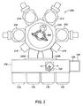
[0039]別の仕方として、前述したような方法は、基板が基板貯蔵装置、基板バッファを有する寄生デバイス及びあるツールの間で移送されるような他の処理システムにおいても使用することができる。例えば、図2は、本発明を効果的に使用することができるような半導体処理のための典型的クラスタツールの概略平面図である。このクラスタツール200は、一般的には、複数の処理チャンバ214を周りに取り付けた中央真空移送チャンバ210を備える。これら処理チャンバ214は、半導体基板に対する所望の特定の処理、例えば、基板上への物質の堆積又は基板上の物質のエッチングを行うために選択される。冷却又は脱気チャンバの如き付加的なチャンバ216を、移送チャンバ210に取り付けることもできる。
[0039] Alternatively, the method as described above can be used in other processing systems where the substrate is transferred between a substrate storage device, a parasitic device having a substrate buffer, and certain tools. For example, FIG. 2 is a schematic plan view of an exemplary cluster tool for semiconductor processing such that the present invention can be effectively used. The
[0040]基板を移送チャンバ210に対して入れたり出したりするために、インバウンドロードロック220A及びアウトバウンドロードロック220Bが設けられ、これらは、システム200内にて実施されるとき方法400についての移送ステーション120A、120Bと同様のものである。ロボット204は、典型的には、移送チャンバ210内に配設され、処理チャンバ214とロードロック220A及び220Bとの間の基板の移送を行う。工場インターフェースモジュール108は、処理中に、工場インターフェースロボット122が基板をロードロック220A、220BとFOUP110との間に移送できるように、ロードロック220A及び220Bに隣接させられている。移送チャンバ110に対する出し入れの両方を行うのに、複数の基板を取り扱うことのできる単一のロードロックを使用することも考えられる。
[0040] An
[0041]例えば、ここに説明した方法を効果的に使用するのに適したプラットフォームとしては、CENTURA(登録名)、PRODUCER(登録名)、ENDURA(登録名)処理プラットフォームがあり、これらは、共に、カリフォルニア州サンタクララのアプライドマテリアルズ社から手に入れることができるものであり、同様に、他の製造者から手に入れることのできるその他のシステムもある。このような1つのステージド真空基板処理システムについて、1993年2月16日付けで発行されたTepman氏等の「Staged-Vacuum Substrate Processing System and Method」と題する米国特許第5,186,718号に詳細に開示されている。その他のクラスタツール及び処理システムも、ここに説明した本発明を適用して効果のあるものであると考えられる。 [0041] For example, suitable platforms for effectively using the methods described herein include CENTURA (registered name), PRODUCER (registered name), and ENDURA (registered name) processing platforms, which are both Available from Applied Materials, Santa Clara, California, as well as other systems available from other manufacturers. One such staged vacuum substrate processing system is disclosed in US Pat. No. 5,186,718 entitled “Staged-Vacuum Substrate Processing System and Method” issued by Tepman et al. It is disclosed in detail. Other cluster tools and processing systems are also considered to be effective by applying the present invention described herein.
[0042]本発明の実施形態について前述したのであるが、本発明の基本的な範囲から逸脱せずに本発明のその他の及び更に別の実施形態を考えることができるのであり、本発明の範囲は、特許請求の範囲によって定められるものである。 [0042] While embodiments of the invention have been described above, other and further embodiments of the invention can be devised without departing from the basic scope thereof, and the scope of the invention Is defined by the claims.
100…システム、102…ポリッシャー、104…ウエットロボット、106…クリーナー、108…工場インターフェースモジュール、110…前面開口部統合ポッド(FOUP)、112…研磨ステーション、114…ロボット、116…ロボットインターフェース、118…移送ステーション、120A…インバウンド移送ステーション、120B…アウトバウンド移送ステーション、122…工場インターフェースロボット、126…寄生デバイス、128…バッファステーション、130…内部ロボット、200…システム、204…ロボット、210…移送チャンバ、214…処理チャンバ、216…付加的なチャンバ、220A…インバウンドロードロック、220B…アウトバウンドロードロック、302…取付けブラケット、304…支持アーム、306A…基板ホルダー、306B…基板ホルダー
DESCRIPTION OF
Claims (14)
FOUPから上記デバイスのために働くバッファステーションへと上記工場インターフェースロボットのエンドエフェクタにて第1の基板を移送するステップと、
上記第1の基板を上記バッファステーションから上記デバイスへ移動させるステップと、
上記処理ツールの上記アウトバウンド移送ステーションから上記エンドエフェクタにて第2の基板をピックアップするステップと、
上記デバイスのために働くバッファステーションへローディングされる上記第2の基板を有する上記工場インターフェースロボットの到着時間を、上記デバイスにおける上記第1の基板の処理の完了と同期させることで、上記デバイスにおける上記第1の基板の寄生処理時間を補償するステップであって、当該補償には、上記デバイスが第2の基板を受け入れ可能となるのを待機し、それから上記第2の基板を上記バッファステーションに隣接する位置に移動させることが含まれるステップと、
上記第2の基板を上記エンドエフェクタから上記デバイスのために働く上記バッファステーションへ移送するステップと、
上記バッファステーションから上記第2の基板をピックアップするステップと、
を備えた方法。 In a system having a factory interface robot, at least one FOUP and a buffer station coupled to a device that performs at least one of substrate orientation, heat treatment, optical metrology, micro-dimension measurement, and film thickness profiling; In a method for transferring a substrate between inbound and outbound transfer stations coupled to a processing tool,
Transferring a first substrate from a FOUP to a buffer station working for the device at an end effector of the factory interface robot;
Moving the first substrate from the buffer station to the device;
Picking up a second substrate at the end effector from the outbound transfer station of the processing tool;
Synchronizing the arrival time of the factory interface robot with the second substrate loaded into the buffer station serving for the device with the completion of processing of the first substrate at the device, thereby Compensating for parasitic processing time of the first substrate, waiting for the device to accept the second substrate, and then adjoining the second substrate to the buffer station. A step including moving to a position to be
Transferring the second substrate from the end effector to the buffer station serving for the device;
Picking up the second substrate from the buffer station;
With a method.
上記処理ツールにおいて上記第1の基板を平坦化するステップと、
上記第2の基板を上記FOUPへ移送するステップと、
を更に備えた、請求項1に記載の方法。 Transferring the first substrate to the inbound transfer station of the processing tool;
Planarizing the first substrate in the processing tool;
Transferring the second substrate to the FOUP;
The method of claim 1, further comprising:
基板の配向、熱処理、光学度量衡、微小寸法測定、及び膜厚プロファイリングの内の少なくとも一つが実行されるデバイスに結合されたバッファと、処理ツールに結合されたインバウンド及びアウトバウンド移送ステーションとの間で基板を移送する方法において、
(a)第1のインバウンド基板を上記ロボットから上記バッファへ入れるステップと、
(b)上記ロボットで第1のアウトバウンド基板を上記バッファから取り出すステップと、
(c)上記第1のアウトバウンド基板を上記ロボットから上記FOUPへ入れるステップと、
(d)上記ロボットで第2のアウトバウンド基板を上記アウトバウンド移送ステーションから取り出すステップと、
(e)上記第2のアウトバウンド基板の上記バッファへの到着時間を、上記デバイスによる上記第1のインバウンド基板の上記バッファへのローディングの完了と同期させるステップであって、当該同期には、上記ロボットが上記第2のアウトバウンド基板を保持した状態の下で、上記デバイスが第2のアウトバウンド基板を受け入れ可能となるのを待機し、それから上記第2のアウトバウンド基板を上記バッファステーションに隣接する位置に移動させることが含まれるステップと、
(f)上記第2のアウトバウンド基板を上記ロボットから上記バッファへ入れ、上記ロボットで上記第1のインバウンド基板を上記バッファから取り出すステップと、
(g)上記第1のインバウンド基板を上記ロボットから上記インバウンド移送ステーションへ入れるステップと、
(h)上記ロボットで第2のインバウンド基板を上記FOUPから取り出すステップと、
(i)上記第2のインバウンド基板の上記バッファへの到着時間を、上記デバイスによる上記第2のアウトバウンド基板の上記バッファへのローディングの完了と同期させるステップであって、当該同期には、上記ロボットが上記第2のインバウンド基板を保持した状態の下で、上記デバイスが第2のインバウンド基板を受け入れ可能となるのを待機し、それから上記第2のインバウンド基板を上記バッファステーションに隣接する位置に移動させることが含まれるステップと、
を順次行うことを備えた方法。 In a system having a factory interface robot, at least one FOUP;
A substrate between a buffer coupled to a device on which at least one of substrate orientation, heat treatment, optical metrology, micro-dimension measurement, and film thickness profiling is performed, and inbound and outbound transfer stations coupled to a processing tool In the method of transporting
(A) placing a first inbound substrate from the robot into the buffer;
(B) removing the first outbound substrate from the buffer with the robot;
(C) placing the first outbound board from the robot into the FOUP;
(D) removing the second outbound substrate from the outbound transfer station with the robot;
(E) Synchronizing the arrival time of the second outbound board to the buffer with the completion of loading of the first inbound board into the buffer by the device , wherein the synchronization includes the robot While holding the second outbound substrate, waits for the device to accept the second outbound substrate, and then moves the second outbound substrate to a position adjacent to the buffer station The steps involved in :
(F) placing the second outbound substrate from the robot into the buffer, and removing the first inbound substrate from the buffer with the robot;
(G) placing the first inbound substrate from the robot into the inbound transfer station;
(H) removing the second inbound substrate from the FOUP with the robot;
(I) synchronizing the arrival time of the second inbound board to the buffer with the completion of loading of the second outbound board into the buffer by the device , wherein the robot includes the robot Holding the second inbound board, waits for the device to accept the second inbound board, and then moves the second inbound board to a position adjacent to the buffer station The steps involved in :
A method comprising sequentially performing.
Applications Claiming Priority (5)
| Application Number | Priority Date | Filing Date | Title |
|---|---|---|---|
| US63849304P | 2004-12-23 | 2004-12-23 | |
| US60/638,493 | 2004-12-23 | ||
| US11/271,242 | 2005-11-10 | ||
| US11/271,242 US7314808B2 (en) | 2004-12-23 | 2005-11-10 | Method for sequencing substrates |
| PCT/US2005/042169 WO2006071406A2 (en) | 2004-12-23 | 2005-11-16 | Method for sequencing substrates |
Publications (2)
| Publication Number | Publication Date |
|---|---|
| JP2008526020A JP2008526020A (en) | 2008-07-17 |
| JP5238263B2 true JP5238263B2 (en) | 2013-07-17 |
Family
ID=35967040
Family Applications (1)
| Application Number | Title | Priority Date | Filing Date |
|---|---|---|---|
| JP2007548232A Active JP5238263B2 (en) | 2004-12-23 | 2005-11-16 | How to sequence a board |
Country Status (4)
| Country | Link |
|---|---|
| US (2) | US7314808B2 (en) |
| JP (1) | JP5238263B2 (en) |
| TW (1) | TWI336095B (en) |
| WO (1) | WO2006071406A2 (en) |
Families Citing this family (12)
| Publication number | Priority date | Publication date | Assignee | Title |
|---|---|---|---|---|
| WO2006004718A1 (en) * | 2004-06-28 | 2006-01-12 | Brooks Automation, Inc. | Non productive wafer buffer module for substrate processing apparatus |
| JP5505384B2 (en) * | 2011-08-04 | 2014-05-28 | 東京エレクトロン株式会社 | Substrate processing apparatus, substrate processing method, and storage medium |
| US20130115862A1 (en) * | 2011-11-09 | 2013-05-09 | Applied Materials, Inc. | Chemical mechanical polishing platform architecture |
| JP6536090B2 (en) * | 2015-03-06 | 2019-07-03 | シンフォニアテクノロジー株式会社 | Transport device |
| CN108347920B (en) * | 2015-08-04 | 2022-04-26 | 罗地亚经营管理公司 | Agricultural adjuvant compositions and methods of using such compositions |
| US10043693B1 (en) * | 2017-06-06 | 2018-08-07 | Applied Materials, Inc. | Method and apparatus for handling substrates in a processing system having a buffer chamber |
| US11469096B2 (en) | 2019-05-03 | 2022-10-11 | Applied Materials, Inc. | Method and chamber for backside physical vapor deposition |
| EP4210903A2 (en) * | 2020-09-08 | 2023-07-19 | Applied Materials, Inc. | Substrate handling systems and methods for cmp processing |
| US11551942B2 (en) | 2020-09-15 | 2023-01-10 | Applied Materials, Inc. | Methods and apparatus for cleaning a substrate after processing |
| US11929264B2 (en) | 2021-03-03 | 2024-03-12 | Applied Materials, Inc. | Drying system with integrated substrate alignment stage |
| US20220310424A1 (en) * | 2021-03-25 | 2022-09-29 | Applied Materials, Inc. | Automated dry-in dry-out dual side polishing of silicon substrates with integrated spin rinse dry and metrology |
| US20230113673A1 (en) * | 2021-10-12 | 2023-04-13 | Applied Materials, Inc. | Factory interface robots usable with integrated load locks |
Family Cites Families (32)
| Publication number | Priority date | Publication date | Assignee | Title |
|---|---|---|---|---|
| US3968885A (en) * | 1973-06-29 | 1976-07-13 | International Business Machines Corporation | Method and apparatus for handling workpieces |
| US5240546A (en) * | 1991-04-26 | 1993-08-31 | Sumitomo Electric Industries, Ltd. | Apparatus for peeling semiconductor substrate |
| JP3130630B2 (en) * | 1992-02-13 | 2001-01-31 | 東京エレクトロン株式会社 | Processing equipment |
| US5658183A (en) * | 1993-08-25 | 1997-08-19 | Micron Technology, Inc. | System for real-time control of semiconductor wafer polishing including optical monitoring |
| FR2711125B1 (en) * | 1993-10-13 | 1996-01-26 | Dubuit Mach | Charger for printing machine for objects presented in stack. |
| US5518542A (en) * | 1993-11-05 | 1996-05-21 | Tokyo Electron Limited | Double-sided substrate cleaning apparatus |
| JPH07211764A (en) * | 1994-01-20 | 1995-08-11 | Nikon Corp | Laser application device |
| US5700046A (en) * | 1995-09-13 | 1997-12-23 | Silicon Valley Group, Inc. | Wafer gripper |
| US5893794A (en) * | 1996-02-28 | 1999-04-13 | Ebara Corporation | Polishing apparatus having robotic transport apparatus |
| US5944857A (en) | 1997-05-08 | 1999-08-31 | Tokyo Electron Limited | Multiple single-wafer loadlock wafer processing apparatus and loading and unloading method therefor |
| US6110011A (en) | 1997-11-10 | 2000-08-29 | Applied Materials, Inc. | Integrated electrodeposition and chemical-mechanical polishing tool |
| JPH11340297A (en) * | 1998-05-21 | 1999-12-10 | Dainippon Screen Mfg Co Ltd | Method and device for transporting substrate |
| US6000998A (en) * | 1998-05-29 | 1999-12-14 | Seh America, Inc. | System for calibrating wafer edge-grinder |
| JP2000012647A (en) * | 1998-06-19 | 2000-01-14 | Sumitomo Eaton Noba Kk | Device and method for carrying wafer |
| IL128087A (en) | 1999-01-17 | 2002-04-21 | Nova Measuring Instr Ltd | Buffer station for a wafer handling system |
| US6358128B1 (en) * | 1999-03-05 | 2002-03-19 | Ebara Corporation | Polishing apparatus |
| US6244931B1 (en) | 1999-04-02 | 2001-06-12 | Applied Materials, Inc. | Buffer station on CMP system |
| US6852012B2 (en) * | 2000-03-17 | 2005-02-08 | Wafer Solutions, Inc. | Cluster tool systems and methods for in fab wafer processing |
| US6891627B1 (en) * | 2000-09-20 | 2005-05-10 | Kla-Tencor Technologies Corp. | Methods and systems for determining a critical dimension and overlay of a specimen |
| JP2002134587A (en) * | 2000-10-26 | 2002-05-10 | Tokyo Electron Ltd | Mechanism for conveying object to be processed and processing system |
| JP2002184834A (en) * | 2000-12-15 | 2002-06-28 | Yaskawa Electric Corp | Substrate transfer robot |
| JP3878441B2 (en) * | 2001-07-18 | 2007-02-07 | 大日本スクリーン製造株式会社 | Substrate processing equipment |
| US20030045098A1 (en) * | 2001-08-31 | 2003-03-06 | Applied Materials, Inc. | Method and apparatus for processing a wafer |
| US7236847B2 (en) * | 2002-01-16 | 2007-06-26 | Kla-Tencor Technologies Corp. | Systems and methods for closed loop defect reduction |
| US20040007325A1 (en) * | 2002-06-11 | 2004-01-15 | Applied Materials, Inc. | Integrated equipment set for forming a low K dielectric interconnect on a substrate |
| US7243003B2 (en) * | 2002-08-31 | 2007-07-10 | Applied Materials, Inc. | Substrate carrier handler that unloads substrate carriers directly from a moving conveyor |
| JP2004119401A (en) * | 2002-09-20 | 2004-04-15 | Foi:Kk | Substrate processing system |
| US6696367B1 (en) | 2002-09-27 | 2004-02-24 | Asm America, Inc. | System for the improved handling of wafers within a process tool |
| JP2004235516A (en) * | 2003-01-31 | 2004-08-19 | Trecenti Technologies Inc | Purging method in wafer housing jig, load port, and method for manufacturing semiconductor device |
| JP2004297040A (en) * | 2003-03-12 | 2004-10-21 | Seiko Epson Corp | Transfer device, transport device, and transfer method |
| US7010388B2 (en) * | 2003-05-22 | 2006-03-07 | Axcelis Technologies, Inc. | Work-piece treatment system having load lock and buffer |
| EP1684951B1 (en) * | 2003-11-10 | 2014-05-07 | Brooks Automation, Inc. | System for handling workpieces in a vacuum-based semiconductor handling system |
-
2005
- 2005-11-10 US US11/271,242 patent/US7314808B2/en not_active Expired - Fee Related
- 2005-11-16 JP JP2007548232A patent/JP5238263B2/en active Active
- 2005-11-16 WO PCT/US2005/042169 patent/WO2006071406A2/en active Application Filing
- 2005-11-17 TW TW094140478A patent/TWI336095B/en active
-
2007
- 2007-12-21 US US11/963,219 patent/US20080093022A1/en not_active Abandoned
Also Published As
| Publication number | Publication date |
|---|---|
| US7314808B2 (en) | 2008-01-01 |
| WO2006071406A3 (en) | 2006-10-05 |
| JP2008526020A (en) | 2008-07-17 |
| US20060183408A1 (en) | 2006-08-17 |
| TW200623217A (en) | 2006-07-01 |
| TWI336095B (en) | 2011-01-11 |
| US20080093022A1 (en) | 2008-04-24 |
| WO2006071406A2 (en) | 2006-07-06 |
Similar Documents
| Publication | Publication Date | Title |
|---|---|---|
| JP5238263B2 (en) | How to sequence a board | |
| US6887124B2 (en) | Method of polishing and cleaning substrates | |
| US8500915B2 (en) | Substrate transporting apparatus, substrate platform shelf and substrate processing apparatus | |
| KR101629627B1 (en) | Substrate processing system, substrate processing method, and computer storage medium | |
| US20060035569A1 (en) | Integrated system for processing semiconductor wafers | |
| US20090025749A1 (en) | Method for vertical transfer of semiconductor substrates in a cleaning module | |
| US7101259B2 (en) | Polishing method and apparatus | |
| US8322963B2 (en) | End effector for a cluster tool | |
| TW201015659A (en) | Work-piece transfer systems and methods | |
| JP4448130B2 (en) | Substrate handler and semiconductor substrate cleaning system | |
| US5330577A (en) | Semiconductor fabrication equipment | |
| JP7329391B2 (en) | Substrate processing method and substrate processing system | |
| CN108064413A (en) | For dry process and the electric hybrid board processing system and its substrate processing method using same of wet processed | |
| US7067015B2 (en) | Modified clean chemistry and megasonic nozzle for removing backside CMP slurries | |
| US20090280727A1 (en) | Polishing system with three headed carousel | |
| JP2005517308A (en) | Integrated semiconductor wafer processing system | |
| WO2023106086A1 (en) | Substrate processing method and substrate processing system | |
| WO2003011518A1 (en) | Cmp system and method for efficiently processing semiconductor wafers | |
| TW202318501A (en) | Substrate processing method and substrate processing system | |
| TW202302271A (en) | Automated dry-in dry-out dual side polishing of silicon substrates with integrated spin rince dry and metrology | |
| US20050069399A1 (en) | Apparatus and method for dry-loading of substrates in scrubber cleaner | |
| WO2024072615A1 (en) | Method and apparatus for processing a substrate in cleaning modules | |
| JPH10107117A (en) | Substrate treating device | |
| US6368882B1 (en) | Method for detecting organic contamination by using hemispherical-grain polysilicon layer | |
| JPH10163145A (en) | Method and device for washing substrate |
Legal Events
| Date | Code | Title | Description |
|---|---|---|---|
| A621 | Written request for application examination |
Free format text: JAPANESE INTERMEDIATE CODE: A621 Effective date: 20080825 |
|
| RD03 | Notification of appointment of power of attorney |
Free format text: JAPANESE INTERMEDIATE CODE: A7423 Effective date: 20101130 |
|
| RD04 | Notification of resignation of power of attorney |
Free format text: JAPANESE INTERMEDIATE CODE: A7424 Effective date: 20101210 |
|
| A977 | Report on retrieval |
Free format text: JAPANESE INTERMEDIATE CODE: A971007 Effective date: 20110419 |
|
| A131 | Notification of reasons for refusal |
Free format text: JAPANESE INTERMEDIATE CODE: A131 Effective date: 20110524 |
|
| A601 | Written request for extension of time |
Free format text: JAPANESE INTERMEDIATE CODE: A601 Effective date: 20110819 |
|
| A602 | Written permission of extension of time |
Free format text: JAPANESE INTERMEDIATE CODE: A602 Effective date: 20110826 |
|
| A601 | Written request for extension of time |
Free format text: JAPANESE INTERMEDIATE CODE: A601 Effective date: 20110926 |
|
| A602 | Written permission of extension of time |
Free format text: JAPANESE INTERMEDIATE CODE: A602 Effective date: 20111003 |
|
| A601 | Written request for extension of time |
Free format text: JAPANESE INTERMEDIATE CODE: A601 Effective date: 20111024 |
|
| A602 | Written permission of extension of time |
Free format text: JAPANESE INTERMEDIATE CODE: A602 Effective date: 20111031 |
|
| A521 | Request for written amendment filed |
Free format text: JAPANESE INTERMEDIATE CODE: A523 Effective date: 20111124 |
|
| A131 | Notification of reasons for refusal |
Free format text: JAPANESE INTERMEDIATE CODE: A131 Effective date: 20120328 |
|
| A601 | Written request for extension of time |
Free format text: JAPANESE INTERMEDIATE CODE: A601 Effective date: 20120625 |
|
| A602 | Written permission of extension of time |
Free format text: JAPANESE INTERMEDIATE CODE: A602 Effective date: 20120702 |
|
| A601 | Written request for extension of time |
Free format text: JAPANESE INTERMEDIATE CODE: A601 Effective date: 20120730 |
|
| A602 | Written permission of extension of time |
Free format text: JAPANESE INTERMEDIATE CODE: A602 Effective date: 20120806 |
|
| A521 | Request for written amendment filed |
Free format text: JAPANESE INTERMEDIATE CODE: A523 Effective date: 20120927 |
|
| TRDD | Decision of grant or rejection written | ||
| A01 | Written decision to grant a patent or to grant a registration (utility model) |
Free format text: JAPANESE INTERMEDIATE CODE: A01 Effective date: 20130305 |
|
| A61 | First payment of annual fees (during grant procedure) |
Free format text: JAPANESE INTERMEDIATE CODE: A61 Effective date: 20130401 |
|
| R150 | Certificate of patent or registration of utility model |
Free format text: JAPANESE INTERMEDIATE CODE: R150 Ref document number: 5238263 Country of ref document: JP Free format text: JAPANESE INTERMEDIATE CODE: R150 |
|
| FPAY | Renewal fee payment (event date is renewal date of database) |
Free format text: PAYMENT UNTIL: 20160405 Year of fee payment: 3 |
|
| R250 | Receipt of annual fees |
Free format text: JAPANESE INTERMEDIATE CODE: R250 |
|
| R250 | Receipt of annual fees |
Free format text: JAPANESE INTERMEDIATE CODE: R250 |
|
| R250 | Receipt of annual fees |
Free format text: JAPANESE INTERMEDIATE CODE: R250 |
|
| R250 | Receipt of annual fees |
Free format text: JAPANESE INTERMEDIATE CODE: R250 |
|
| R250 | Receipt of annual fees |
Free format text: JAPANESE INTERMEDIATE CODE: R250 |