JP5199824B2 - Tilt sensor and manufacturing method thereof - Google Patents
Tilt sensor and manufacturing method thereof Download PDFInfo
- Publication number
- JP5199824B2 JP5199824B2 JP2008274496A JP2008274496A JP5199824B2 JP 5199824 B2 JP5199824 B2 JP 5199824B2 JP 2008274496 A JP2008274496 A JP 2008274496A JP 2008274496 A JP2008274496 A JP 2008274496A JP 5199824 B2 JP5199824 B2 JP 5199824B2
- Authority
- JP
- Japan
- Prior art keywords
- light
- plating layer
- pair
- receiving elements
- protrusions
- Prior art date
- Legal status (The legal status is an assumption and is not a legal conclusion. Google has not performed a legal analysis and makes no representation as to the accuracy of the status listed.)
- Active
Links
Images


Classifications
-
- G—PHYSICS
- G01—MEASURING; TESTING
- G01C—MEASURING DISTANCES, LEVELS OR BEARINGS; SURVEYING; NAVIGATION; GYROSCOPIC INSTRUMENTS; PHOTOGRAMMETRY OR VIDEOGRAMMETRY
- G01C9/00—Measuring inclination, e.g. by clinometers, by levels
- G01C9/02—Details
- G01C9/06—Electric or photoelectric indication or reading means
-
- C—CHEMISTRY; METALLURGY
- C25—ELECTROLYTIC OR ELECTROPHORETIC PROCESSES; APPARATUS THEREFOR
- C25D—PROCESSES FOR THE ELECTROLYTIC OR ELECTROPHORETIC PRODUCTION OF COATINGS; ELECTROFORMING; APPARATUS THEREFOR
- C25D5/00—Electroplating characterised by the process; Pretreatment or after-treatment of workpieces
- C25D5/02—Electroplating of selected surface areas
- C25D5/022—Electroplating of selected surface areas using masking means
-
- C—CHEMISTRY; METALLURGY
- C25—ELECTROLYTIC OR ELECTROPHORETIC PROCESSES; APPARATUS THEREFOR
- C25D—PROCESSES FOR THE ELECTROLYTIC OR ELECTROPHORETIC PRODUCTION OF COATINGS; ELECTROFORMING; APPARATUS THEREFOR
- C25D5/00—Electroplating characterised by the process; Pretreatment or after-treatment of workpieces
- C25D5/10—Electroplating with more than one layer of the same or of different metals
- C25D5/12—Electroplating with more than one layer of the same or of different metals at least one layer being of nickel or chromium
-
- C—CHEMISTRY; METALLURGY
- C25—ELECTROLYTIC OR ELECTROPHORETIC PROCESSES; APPARATUS THEREFOR
- C25D—PROCESSES FOR THE ELECTROLYTIC OR ELECTROPHORETIC PRODUCTION OF COATINGS; ELECTROFORMING; APPARATUS THEREFOR
- C25D5/00—Electroplating characterised by the process; Pretreatment or after-treatment of workpieces
- C25D5/627—Electroplating characterised by the visual appearance of the layers, e.g. colour, brightness or mat appearance
-
- G—PHYSICS
- G01—MEASURING; TESTING
- G01C—MEASURING DISTANCES, LEVELS OR BEARINGS; SURVEYING; NAVIGATION; GYROSCOPIC INSTRUMENTS; PHOTOGRAMMETRY OR VIDEOGRAMMETRY
- G01C9/00—Measuring inclination, e.g. by clinometers, by levels
- G01C9/10—Measuring inclination, e.g. by clinometers, by levels by using rolling bodies, e.g. spheres, cylinders, mercury droplets
-
- G—PHYSICS
- G01—MEASURING; TESTING
- G01C—MEASURING DISTANCES, LEVELS OR BEARINGS; SURVEYING; NAVIGATION; GYROSCOPIC INSTRUMENTS; PHOTOGRAMMETRY OR VIDEOGRAMMETRY
- G01C9/00—Measuring inclination, e.g. by clinometers, by levels
- G01C9/02—Details
- G01C9/06—Electric or photoelectric indication or reading means
- G01C2009/066—Electric or photoelectric indication or reading means optical
Landscapes
- Chemical & Material Sciences (AREA)
- Engineering & Computer Science (AREA)
- Organic Chemistry (AREA)
- Electrochemistry (AREA)
- Materials Engineering (AREA)
- Metallurgy (AREA)
- Chemical Kinetics & Catalysis (AREA)
- Physics & Mathematics (AREA)
- General Physics & Mathematics (AREA)
- Radar, Positioning & Navigation (AREA)
- Remote Sensing (AREA)
- Length Measuring Devices By Optical Means (AREA)
- Manufacture Of Switches (AREA)
- Light Receiving Elements (AREA)
- Fire-Detection Mechanisms (AREA)
Description
本発明は、たとえばデジタルスチルカメラなどの傾斜方向を検出するための傾斜センサおよびその製造方法に関する。 The present invention relates to a tilt sensor for detecting a tilt direction of, for example, a digital still camera and a method for manufacturing the tilt sensor.
図15は、従来の傾斜センサの一例を示している。同図に示された傾斜センサXは、基板91、ケース92、カバー93、1対の受光素子94A,94B、発光素子95、および転動体96を備えている。ケース92には上方に開口する凹部が形成されている。この凹部をカバー93が覆うことにより、空隙部92aが形成されている。空隙部92aには、転動体96が収容されている。1対の受光素子94A,94Bおよび発光素子95は、基板91に搭載されている。発光素子95からの光は、空隙部92aに向けて発せられる。この光は、カバー93に設けられた反射膜93aによって反射される。転動体96は、重力方向の変化に応じて空隙部92a内を転動することにより、受光素子94Aに重なる位置と、受光素子94Bに重なる位置と、発光素子95に重なる位置とをとる。これにより、転動体96の位置によって、発光素子95からの光が、受光素子94Aのみによって受光される場合、受光素子94Bのみによって受光される場合、および1対の受光素子94A,94Bのいずれによっても受光されない場合が存在する。したがって、1対の受光素子94A,94Bの受光状態を監視することにより、基板91の面内方向における傾斜を検出することができる。
FIG. 15 shows an example of a conventional tilt sensor. The tilt sensor X shown in the figure includes a
しかしながら、傾斜センサXによって傾斜を正確に検出するには、転動体96が空隙部92a内においてスムーズに転動することが必要である。転動体96がケース92またはカバー93に固着してしまうと、重力方向の変化があっても転動体96が適切に転動しない。このようなことでは、傾斜を正しく検出することができない。傾斜センサXの小型化を図るほど、傾斜センサXの製造工程において、あるいは使用を重ねた後に、転動体96がカバー93に対して固着することがあった。
However, in order to accurately detect the tilt by the tilt sensor X, the
本発明は、上記した事情のもとで考え出されたものであって、転動体をスムーズに転動させることが可能な傾斜センサを提供することをその課題とする。 The present invention has been conceived under the above circumstances, and an object thereof is to provide an inclination sensor capable of smoothly rolling a rolling element.
本発明の第1の側面によって提供される傾斜センサは、検出対象面の面内方向において互いに離間配置された発光素子および1対の受光素子と、上記面内方向における重力方向の変化により、上記発光素子からの光を上記1対の受光素子のいずれにも到達させない完全遮光位置、上記発光素子からの光を上記1対の受光素子のいずれか一方のみに到達させる1対の半遮光位置、および上記発光素子からの光を上記1対の受光素子のいずれにも到達させる非遮光位置をとる転動体と、上記転動体を収容し、かつ上記発光素子からの光が出射される出射口および上記1対の受光素子に向けて光が入射する1対の入射口に繋がる空隙部と、を備える傾斜センサであって、上記面内方向に広がり上記空隙部に露出するとともに凹凸状とされた天井面を備えており、上記転動体は、その軸方向が上記面内方向と直角である円柱形状であるとともに、上記天井面は、それぞれの上記面内方向面積が上記転動体よりも小である複数の突起が形成された部分の表面であって、上記各突起は、上記面内方向形状が円形であることを特徴としている。 The tilt sensor provided by the first aspect of the present invention includes a light emitting element and a pair of light receiving elements that are spaced apart from each other in the in-plane direction of the detection target surface, and a change in the gravitational direction in the in-plane direction. A completely light-shielding position where light from the light-emitting element does not reach any of the pair of light-receiving elements, a pair of semi-light-shielding positions where light from the light-emitting element reaches only one of the pair of light-receiving elements, And a rolling element that takes a non-light-shielding position that allows light from the light emitting element to reach any of the pair of light receiving elements, an exit opening that accommodates the rolling element and emits light from the light emitting element, and An inclination sensor connected to a pair of incident ports through which light is incident toward the pair of light receiving elements, the inclination sensor extending in the in-plane direction and exposed to the gap, and having an uneven shape. Ceiling E is, the rolling elements, with the axial direction of a cylindrical shape that is perpendicular to the direction within the plane, the ceiling surface, each said plane direction area of the plurality is smaller than the rolling elements a surface of the projections are formed portion, said each projection, the in-plane direction shape is characterized by a circular der Rukoto.
このような構成によれば、上記転動体が上記天井面に固着することを抑制することが可能であり、傾斜方向を正確に検出することができる。またこのような構成によれば、上記転動体が、上記発光素子からの光を好適に遮蔽しつつ、スムーズに転動しやすい。また、このような構成によれば、上記転動体の固着を防止するのに好ましい。 According to such a configuration, it is possible to suppress the rolling element from adhering to the ceiling surface, and the inclination direction can be accurately detected. Moreover, according to such a structure, the said rolling element is easy to roll smoothly, shielding the light from the said light emitting element suitably. Moreover, according to such a structure, it is preferable to prevent the rolling elements from sticking.
本発明の第2の側面によって提供される傾斜センサは、検出対象面の面内方向において互いに離間配置された発光素子および1対の受光素子と、上記面内方向における重力方向の変化により、上記発光素子からの光を上記1対の受光素子のいずれにも到達させない完全遮光位置、上記発光素子からの光を上記1対の受光素子のいずれか一方のみに到達させる1対の半遮光位置、および上記発光素子からの光を上記1対の受光素子のいずれにも到達させる非遮光位置をとる転動体と、上記転動体を収容し、かつ上記発光素子からの光が出射される出射口および上記1対の受光素子に向けて光が入射する1対の入射口に繋がる空隙部と、を備える傾斜センサであって、上記面内方向に広がり上記空隙部に露出するとともに凹凸状とされた天井面を備えており、上記転動体は、その軸方向が上記面内方向と直角である円柱形状であるとともに、上記天井面は、それぞれの上記面内方向面積が上記転動体よりも小である複数の突起が形成された部分の表面であって、上記複数の突起は、互いに放射状に配置された長細状のものを含むことを特徴としている。 The tilt sensor provided by the second aspect of the present invention includes a light emitting element and a pair of light receiving elements that are spaced apart from each other in the in-plane direction of the detection target surface, and a change in the gravitational direction in the in-plane direction. A completely light-shielding position where light from the light-emitting element does not reach any of the pair of light-receiving elements, a pair of semi-light-shielding positions where light from the light-emitting element reaches only one of the pair of light-receiving elements, And a rolling element that takes a non-light-shielding position that allows light from the light emitting element to reach any of the pair of light receiving elements, an exit opening that accommodates the rolling element and emits light from the light emitting element, and An inclination sensor connected to a pair of incident ports through which light is incident toward the pair of light receiving elements, the inclination sensor extending in the in-plane direction and exposed to the gap, and having an uneven shape. Ceiling The rolling element has a cylindrical shape whose axial direction is perpendicular to the in-plane direction, and the ceiling surface has a plurality of protrusions each having an area in the in-plane direction smaller than that of the rolling element. The plurality of protrusions include a long surface that is radially arranged with respect to the surface of the portion formed with.
本発明の好ましい実施の形態においては、上記複数の突起の配置ピッチは、上記転動体の直径よりも小である。このような構成によれば、上記転動体が傾いてしまうことを防止するのに適している。 In a preferred embodiment of the present invention, the arrangement pitch of the plurality of protrusions is smaller than the diameter of the rolling element. Such a configuration is suitable for preventing the rolling element from being inclined.
本発明の好ましい実施の形態においては、上記面内方向に対して直角である方向に延び、上記空隙部を囲む内側面を構成するケースと、上記天井面を構成するカバーと、を備えており、上記カバーには、メッキ膜によって上記複数の突起が形成されている。このような構成によれば、上記天井面を凹凸状とするための上記複数の突起を容易に形成することができる。 In a preferred embodiment of the present invention, there is provided a case that extends in a direction perpendicular to the in-plane direction and that forms an inner surface that surrounds the gap, and a cover that forms the ceiling surface. The plurality of protrusions are formed on the cover by a plating film. According to such a configuration, the plurality of protrusions for making the ceiling surface uneven can be easily formed.
本発明の好ましい実施の形態においては、上記カバーには、上記カバーに直接形成されており、上記複数の突起よりも面積が大である下地メッキ層、上記複数の突起と同形状とされた中間メッキ層とが積層されており、上記複数の突起は、上記中間メッキ層上に形成されている。 In a preferred embodiment of the present invention, the cover is directly formed on the cover and has a base plating layer having a larger area than the plurality of protrusions, and an intermediate shape having the same shape as the plurality of protrusions. A plating layer is laminated, and the plurality of protrusions are formed on the intermediate plating layer.
本発明の好ましい実施の形態においては、上記下地メッキ層および上記複数の突起は、Cuからなり、上記中間メッキ層は、上記下地メッキ層側に位置するNi層および上記複数の突起側に位置するCu層からなる。 In a preferred embodiment of the present invention, the base plating layer and the plurality of protrusions are made of Cu, and the intermediate plating layer is positioned on the Ni layer on the base plating layer side and the plurality of protrusions. It consists of a Cu layer.
本発明の好ましい実施の形態においては、上記複数の突起および上記下地メッキ層を覆い、かつ表層がAuメッキ層からなる上メッキ層をさらに備える。 In a preferred embodiment of the present invention, an upper plating layer that covers the plurality of protrusions and the base plating layer and whose surface layer is an Au plating layer is further provided.
本発明の第3の側面によって提供される傾斜センサの製造方法は、検出対象面の面内方向において互いに離間配置された発光素子および1対の受光素子と、上記面内方向における重力方向の変化により、上記発光素子からの光を上記1対の受光素子のいずれにも到達させない完全遮光位置、上記発光素子からの光を上記1対の受光素子のいずれか一方のみに到達させる1対の半遮光位置、および上記発光素子からの光を上記1対の受光素子のいずれにも到達させる非遮光位置をとる転動体と、上記転動体を収容し、かつ上記発光素子からの光が出射される出射口および上記1対の受光素子に向けて光が入射する1対の入射口に繋がる空隙部と、を備える傾斜センサの製造方法であって、板状のカバーに下地メッキ層を形成する工程と、上記下地メッキ層を覆う中間メッキ層を形成する工程と、上記中間メッキ層を覆う1以上の突起準備層を形成する工程と、上記中間メッキ層の一部および上記1以上の突起準備層に対してパターニングを施すことにより、複数の突起を形成する工程と、上記複数の突起および上記下地メッキ層を覆う上メッキ層を形成する工程と、上記カバーを用いて上記空隙部を構成する工程と、を有することを特徴としている。 The tilt sensor manufacturing method provided by the third aspect of the present invention includes a light emitting element and a pair of light receiving elements that are spaced apart from each other in the in-plane direction of the detection target surface, and a change in the gravitational direction in the in-plane direction. Thus, a complete light blocking position where the light from the light emitting element does not reach any of the pair of light receiving elements, and a pair of halves that allow the light from the light emitting element to reach only one of the pair of light receiving elements. A rolling element having a light shielding position and a non-light shielding position that allows light from the light emitting element to reach any of the pair of light receiving elements, and the rolling element is housed and light is emitted from the light emitting element. A step of forming a base plating layer on a plate-like cover, comprising: an exit opening; and a gap portion connected to the pair of entrance openings through which light enters the pair of light receiving elements. And above Forming an intermediate plating layer covering the plating layer; forming one or more protrusion preparation layers covering the intermediate plating layer; patterning a part of the intermediate plating layer and the one or more protrusion preparation layers; Forming a plurality of protrusions, forming an upper plating layer that covers the plurality of protrusions and the base plating layer, and forming the gap using the cover. It is characterized by that.
このような構成によれば、上記転動体をスムーズに転動させることが可能な上記傾斜センサを適切に製造することができる。 According to such a structure, the said inclination sensor which can roll the said rolling element smoothly can be manufactured appropriately.
本発明の好ましい実施の形態においては、上記中間メッキ層は、互いに材質が異なり、上記下地メッキ層側に位置する第1層、および上記複数の突起側に位置する第2層からなり、上記第1層は、上記下地メッキ層と異なる材質からなり、上記第2層は、上記突起準備層と同じ材質からなる。 In a preferred embodiment of the present invention, the intermediate plating layer is made of different materials, and includes a first layer located on the base plating layer side and a second layer located on the plurality of protrusions side. One layer is made of a material different from that of the base plating layer, and the second layer is made of the same material as the protrusion preparation layer.
本発明の好ましい実施の形態においては、上記複数の突起を形成する工程においては、上記第2層および上記1以上の突起準備層を選択的に除去し、かつ上記第1層を残存させるエッチングを行った後に、上記第1層を選択的に除去し、かつ上記下地メッキ層を残存させるエッチングを行う。このような構成によれば、上記複数の突起を所望の形状に形成しつつ、上記上メッキ層を均一な厚さで形成することができる。 In a preferred embodiment of the present invention, in the step of forming the plurality of protrusions, etching is performed to selectively remove the second layer and the one or more protrusion preparation layers and leave the first layer. After the etching, etching is performed to selectively remove the first layer and leave the base plating layer. According to such a configuration, the upper plating layer can be formed with a uniform thickness while forming the plurality of protrusions in a desired shape.
本発明のその他の特徴および利点は、添付図面を参照して以下に行う詳細な説明によって、より明らかとなろう。 Other features and advantages of the present invention will become more apparent from the detailed description given below with reference to the accompanying drawings.
以下、本発明の好ましい実施の形態につき、図面を参照して具体的に説明する。 Hereinafter, preferred embodiments of the present invention will be specifically described with reference to the drawings.
図1〜図3は、本発明に係る傾斜センサの第1実施形態を示している。本実施形態の傾斜センサA1は、基板1、ケース2、カバー3、1対の受光素子4A,4B、発光素子5、および転動体6を備えている。傾斜センサA1は、たとえば回路基板Sに面実装された状態で、回路基板Sの面内方向における傾斜方向を検出するために用いられるものである。本実施形態においては、傾斜センサA1は、そのサイズが4.2mm×4.2mm程度、厚さが3.0mm程度とされている。なお、図2においては、カバー3を省略している。
1 to 3 show a first embodiment of a tilt sensor according to the present invention. The tilt sensor A1 of the present embodiment includes a
基板1は、矩形状の絶縁基板であり、たとえばガラスエポキシ樹脂からなる。本実施形態においては、基板1は、そのサイズが4.2mm×4.2mm程度、厚さ0.6mm程度とされている。基板1には、配線パターン7が形成されている。配線パターン7は、たとえば銅からなり、銅製の薄膜に対してエッチングを施すことなどにより形成される。配線パターン7は、基板1の表裏面に形成された部分と、これらの部分を導通させるスルーホール部分(図示略)とを有している。配線パターン7のうち基板1の表面に形成された部分には、1対の受光素子4A,4Bおよび発光素子5がダイボンディングされている。図3に示すように、配線パターン7のうち基板1の裏面に形成された部分は、面実装用の端子7a,7bとされている。
The
1対の受光素子4A,4Bは、たとえばPINフォトダイオードであり、赤外線を受光すると、それに応じた光起電力を生じて電流を流すように構成されている。1対の受光素子4A,4Bは、基板1に互いに離間して配置されている。本実施形態においては、受光素子4A,4Bは、そのサイズが0.6mm角程度とされている。
The pair of
発光素子5は、赤外線を発することができる赤外線発光ダイオードなどからなる。発光素子5は、1対の受光素子4A,4Bが離間する方向においてこれらの中間に配置されている。本実施形態においては、発光素子5は、そのサイズが0.25mm角程度とされている。
The
ケース2は、全体が直方体形状であり、たとえば導電性樹脂などの導電性材料によって形成されている。ケース2には、凹部2aが形成されている。凹部2aとこれを塞ぐカバー3とによって、空隙部20aが形成されている。また、ケース2には、3つの窓20b、および3つの素子収容部20cが形成されている。本実施形態においては、ケース2は、そのサイズが4.2mm角程度、厚さが2.0mm程度とされている。
The
ケース2は、基板1に形成された配線パターン7のうちグランド端子(図示略)に導通する部分に接している。これにより、ケース2は、上記グランド端子に導通している。
The
空隙部20aは、転動体6を収容する部分であり、傾斜センサA1の姿勢に応じた所定の位置に転動体6を転動させるための部分である。空隙部20aは、四隅がラウンド状である断面菱形状とされている。本実施形態においては、空隙部20aの断面寸法が、3.0mm角程度とされている。空隙部20aには、3つの窓20bが繋がっている。
The
3つの窓20bは、1対の受光素子4A,4Bへと光を到達させ、または発光素子5からの光を通過させるためのものである。3つの窓20bには、3つの素子収容部20cがそれぞれ繋がっている。3つの素子収容部20cは、1対の受光素子4A,4Bおよび発光素子5を収容するための部分である。受光素子4A,4Bを収容する2つの素子収容部20cに繋がる2つの窓20bが、本発明でいう入射口の一例に相当し、発光素子5を収容する素子収容部20cに繋がる窓20bが、本発明でいう出射口の一例に相当する。
The three
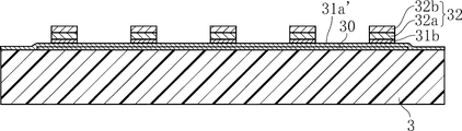
カバー3は、ケース2を塞ぐことにより空隙部20aを形成するためのものであり、例えばガラスエポキシ樹脂からなる。図3に示すように、カバー3には、下地メッキ層30、中間メッキ層31、複数の突起32、および上メッキ層33が形成されている。カバー3は、ケース2に対して接着剤8によって接着されている。
The
下地メッキ層30は、カバー3上に直接形成されており、たとえば厚さ18μm程度のCuメッキ層である。中間メッキ層31は、それぞれが直径0.2mm程度の円形状とされた複数の要素に分割された構成とされており、Niメッキ層31aおよびCuメッキ層31bからなる。Niメッキ層31aは、下地メッキ層30上に形成されており、厚さが3μm程度である。Cuメッキ層31bは、Niメッキ層31a上に形成されており、厚さが5μm程度である。複数の突起32は、平面視において中間メッキ層31と一致するように配置されており、複数のCuメッキ層32a,32bが積層された構造とされている。Cuメッキ層32a,32bは、比較的厚肉であり、本実施形態においてはそれぞれの厚さが25μm程度である。図4に示すように、複数の突起32は、マトリクス状に配置されており、そのピッチは0.45mm程度である。上メッキ層33は、複数の突起32および下地メッキ層30のうち複数の突起32によって覆われていない部分を覆っており、Niメッキ層33aおよびAuメッキ層33bからなる。Niメッキ層33aの厚さが、3μm程度、Auメッキ層33bの厚さが0.03μm程度である。Auメッキ層33bは、発光素子5からの光を反射する機能を果たす。本実施形態においては、Auメッキ層33bの表面が、本発明でいう天井面3aとなっている。
The
転動体6は、傾斜センサA1の姿勢に応じて空隙部20a内を転動することにより、発光素子5からの光が1対の受光素子4A,4Bへと到達することを適宜阻止するためのものである。転動体6は、円柱形状とされており、たとえばステンレスからなる。
The rolling
傾斜センサA1による傾斜方向の検出は、以下のように行われる。図1に示す状態においては、転動体6は、完全遮光位置P1に位置している。このときは、転動体6が発光素子5からの光を完全に遮ることとなり、受光素子4A,4Bは、いずれも受光信号を発しない。図1に示す状態から傾斜センサA1が反時計回りに90度回転すると、転動体6は、半遮光位置P2Aに位置する。このときは、転動体6が受光素子4Aに向かう光を遮り、受光素子4Bのみから受光信号が発せられる。図1に示す状態から傾斜センサA1が時計回りに90度回転すると、転動体6は、半遮光位置P2Bに位置する。このときは、転動体6が受光素子4Bに向かう光を遮り、受光素子4Aのみから受光信号が発せられる。図1に示す状態から傾斜センサA1が180度回転すると、転動体6は、非遮光位置P3に位置する。このときは、受光素子4A,4Bの双方から受光信号が発せられる。このように、受光センサ4A,4Bからの受光信号の有無を監視することにより、傾斜方向の検出を行うことができる。
The inclination direction is detected by the inclination sensor A1 as follows. In the state shown in FIG. 1, the rolling
次に、傾斜センサA1の製造方法の一例について、図5〜図11を参照しつつ、以下に説明する。 Next, an example of a method for manufacturing the tilt sensor A1 will be described below with reference to FIGS.
まず、カバー3に下地メッキ層30を形成する。具体的には、たとえばカバー3の表面全体を覆うように厚さ18μm程度のCuメッキを施した後に、エッチングを用いたパターニングを行う。この結果、図6に示すような形状とされた下地メッキ層30が得られる。
First, the
次に、図7に示すように、下地メッキ層30およびカバー3を覆うように厚さ3μm程度のNiメッキ層31a’を形成する。このNiメッキ層31a’の形成に先立って、下地メッキ層30およびカバー3を覆うように比較的薄い無電解メッキを施しておくことが好ましい。さらに、Niメッキ層31a’を覆うように厚さ5μm程度のCuメッキ層31b’を形成する。
Next, as shown in FIG. 7, a
次いで、図8に示すように、Cuメッキ層31b’上にCuメッキ層32a’,32b’を形成する。これらのCuメッキ層32a’,32b’の厚さは、それぞれ25μm程度とする。
Next, as shown in FIG. 8,
次いで、Cuメッキ層32a’,32b’およびCuメッキ層31b’に対してパターニングを行う。このパターニングは、図4に示す複数の突起32に対応した開口を有するマスクを用いてCuを選択的にエッチングすることによって行う。これにより、図9に示すように、複数の円形要素からなるCuメッキ層31bと、Cuメッキ層32a,32bからなる複数の突起32とが得られる。
Next, patterning is performed on the Cu plating layers 32a 'and 32b' and the
次いで、Niを選択的にエッチングすることによりNiメッキ層31a’に対してパターニングを行う。これにより、図10に示すようにNiメッキ層31aおよびCuメッキ層31bからなる中間メッキ層31が得られる。
Next, the
次いで、図11に示すように、厚さ3μm程度のNiメッキ層33aおよび厚さ0.03μm程度のAuメッキ層33bを順に形成することにより、上メッキ層33が得られる。これらの工程とは別に、基板1への受光素子4A,4Bおよび発光素子5の実装や、ケース2の成形を行う。そして、基板1、ケース2、およびカバー3を張り合わせることにより、傾斜センサA1が得られる。なお、複数の基板1を形成可能な基板材料、複数のケース2を形成可能な樹脂材料、および複数のカバー3を形成可能な樹脂材料を張り合わせた後にこれらを切断することにより、複数の傾斜センナA1を一括して製造してもよい。
Next, as shown in FIG. 11, an
次に、傾斜センサA1およびその製造方法の作用について説明する。 Next, the operation of the tilt sensor A1 and the manufacturing method thereof will be described.
傾斜センサA1において転動体6を天井面3aに固着させる要因としては以下が挙げられる。まず、カバー3およびケース2の間からはみ出してくる接着剤8である。はみ出した接着剤8の量が多いと、転動体6が天井面3aに接着されてしまう。次に、製造工程において浸入した水分である。上述した基板材料と樹脂材料とを接着した後の切断工程においては、潤滑および冷却のために水がかけられる。この水が誤ってカバー3およびケース2のわずかな隙間から空隙部20aに浸入することがある。このような事態を想定して、上記切断工程の後に傾斜センサA1全体を加熱する場合もあるが、浸入した水分をすべて蒸発させられるとは限らない。
The following are examples of factors that cause the rolling
本実施形態においては、はみ出した接着剤8や浸入した水分が天井面3aの凹部にたまる。このため、転動体6と接する天井面3aの凸部は、乾いた状態である。したがって、転動体6が天井面3aに固着することを防止可能であり、傾斜方向を正確に検出することができる。特に、転動体6が円柱状であると、光を遮蔽しつつスムーズに転動するのに適しているが、天井面3aとの接触面積が大きくなる。しかし、凹凸状である天井面3aによって、転動体6が円柱状であっても固着を抑制することができる。
In the present embodiment, the protruding adhesive 8 and the infiltrated water accumulate in the concave portion of the
突起32の平面視面積が転動体6の端面の面積よりも小であることにより、1つの突起32と転動体6全体が隙間なく固着してしまうことを防止できる。複数の突起32のピッチが転動体6の直径よりも小であることにより、転動体6が傾いてしまうことを回避できる。
When the planar view area of the
メッキによって複数の突起32を形成すれば、下地メッキ層30や上メッキ層33を形成するための手法と同等の手法によって形成することができる。これは、製造工程の簡素化に好ましい。
If the plurality of
Niメッキ層31a’を除去するエッチング工程によって、下地メッキ層30の表面が洗浄され、下地メッキ層30の意図しない微小な突起などが除去される。これにより、下地メッキ層30がきわめて平滑な表面性状となり、上メッキ層33を非常に均一に設けることが可能である。これは、発光素子5からの光を適切に反射するのに適している。また、上メッキ層33のうちケース2と重なる部分の厚さが揃っているほど、ケース2に対してカバー3が傾くことを防止するのに都合がよい。
By the etching process for removing the
中間層31を形成するためにNiメッキ層31a’およびCuメッキ層31b’を設けている。Cuメッキ層31b’は、複数の突起32を形成するためのCuメッキ層32a’,32b’と同じ材質である。このため、複数の突起32を形成するためのパターニングにおいて、Cuメッキ層31b’およびCuメッキ層32a’,32b’に対して一括してエッチングを施すとともに、Niメッキ層31a’をいわゆるエッチングストップ層として用いることができる。また、Niメッキ層31a’と下地メッキ層30とが異なる材質であることにより、Niメッキ層31a’をエッチングによって選択的に除去しつつ、下地メッキ層30を洗浄することができる。
In order to form the
図12〜図14は、本発明の他の実施形態を示している。なお、これらの図において、上記実施形態と同一または類似の要素には、上記実施形態と同一の符号を付している。 12 to 14 show another embodiment of the present invention. In these drawings, the same or similar elements as those in the above embodiment are denoted by the same reference numerals as those in the above embodiment.
図12は、複数の突起32の他の例を示している。本図に示す例においては、カバー3に4つの突起が設けられている。各突起32は、細長帯状であり、幅が0.2mm程度、長さが0.9mm程度である。4つの突起32は、カバー3の中心から放射状に配置されており、互いのなす角が90度とされている。対角に位置する突起32どうしの間隔は、0.6mm程度である。このような構成によっても、転動体6をスムーズに転動させることが可能であり、傾斜方向を正確に検出することができる。
FIG. 12 shows another example of the plurality of
図13および図14は、本発明に係る傾斜センサの第2実施形態を示している。本実施形態の傾斜センサA2は、空隙部20aと受光素子4A,4Bおよび発光素子5との配置が上述した実施形態と異なっている。
13 and 14 show a second embodiment of the tilt sensor according to the present invention. In the inclination sensor A2 of this embodiment, the arrangement of the
本実施形態においては、空隙部20aを囲むように3つの素子収容部20cが形成されている。受光素子4A,4Bは、空隙部20aを挟むように配置されている。図14に示すように、窓20bは、カバー3から突出する突起によって高さ方向寸法が減じられている。本実施形態においても、複数の突起32が形成されていることにより、天井面3aが凹凸状とされている。本実施形態においては、完全遮光位置P1、半遮光位置P2A,P2B,および非遮光位置P3は、図13に示すような配置となる。
In the present embodiment, three
このような実施形態によっても、転動体6をスムーズに転動させることが可能であり、傾斜方向を正確に検出することができる。また、本実施形態の傾斜センサA2は、薄型化を図るのに適している。
Also according to such an embodiment, it is possible to roll the rolling
本発明に係る傾斜センサおよびその製造方法は、上述した実施形態に限定されるものではない。本発明に係る傾斜センサおよびその製造方法の具体的な構成は、種々に設計変更自在である。 The tilt sensor and the manufacturing method thereof according to the present invention are not limited to the above-described embodiments. The specific configuration of the tilt sensor and the manufacturing method thereof according to the present invention can be changed in various ways.
A1,A2 傾斜センサ
S 回路基板
1 基板
2 ケース
2a 凹部
3 カバー
3a 天井面
4A,4B 受光素子
5 発光素子
6 転動体
7 配線パターン
7a,7b (面実装用の)端子
20a 空隙部
20b 窓
20c 素子収容部
30 下地メッキ層
31 中間メッキ層
31a Ni層
31b Cu層
32 突起
32a,32b Cuメッキ層
33 上メッキ層
33a Niメッキ層
33b Auメッキ層
A1, A2 Inclination sensor
Claims (10)
上記面内方向における重力方向の変化により、上記発光素子からの光を上記1対の受光素子のいずれにも到達させない完全遮光位置、上記発光素子からの光を上記1対の受光素子のいずれか一方のみに到達させる1対の半遮光位置、および上記発光素子からの光を上記1対の受光素子のいずれにも到達させる非遮光位置をとる転動体と、
上記転動体を収容し、かつ上記発光素子からの光が出射される出射口および上記1対の受光素子に向けて光が入射する1対の入射口に繋がる空隙部と、
を備える傾斜センサであって、
上記面内方向に広がり上記空隙部に露出するとともに凹凸状とされた天井面を備えており、
上記転動体は、その軸方向が上記面内方向と直角である円柱形状であるとともに、
上記天井面は、それぞれの上記面内方向面積が上記転動体よりも小である複数の突起が形成された部分の表面であって、
上記各突起は、上記面内方向形状が円形であることを特徴とする、傾斜センサ。 A light emitting element and a pair of light receiving elements that are spaced apart from each other in the in-plane direction of the detection target surface;
Due to a change in the direction of gravity in the in-plane direction, the light from the light emitting element does not reach any of the pair of light receiving elements, and the light from the light emitting element is any of the pair of light receiving elements. A rolling element having a pair of semi-light-shielding positions that reach only one side and a non-light-shielding position that allows light from the light-emitting elements to reach any of the pair of light-receiving elements;
A gap portion that accommodates the rolling element and is connected to a pair of incident ports through which light enters the pair of light receiving elements and an exit port from which light from the light emitting element is emitted;
An inclination sensor comprising:
It is provided with a ceiling surface that extends in the in-plane direction and is exposed to the gap and is uneven .
The rolling element has a cylindrical shape whose axial direction is perpendicular to the in-plane direction,
The ceiling surface is a surface of a portion where a plurality of projections each having an in-plane direction area smaller than the rolling element is formed,
Said each projection, the in-plane direction shape and wherein the circular der Rukoto, tilt sensor.
上記面内方向における重力方向の変化により、上記発光素子からの光を上記1対の受光素子のいずれにも到達させない完全遮光位置、上記発光素子からの光を上記1対の受光素子のいずれか一方のみに到達させる1対の半遮光位置、および上記発光素子からの光を上記1対の受光素子のいずれにも到達させる非遮光位置をとる転動体と、Due to a change in the direction of gravity in the in-plane direction, the light from the light emitting element does not reach any of the pair of light receiving elements, and the light from the light emitting element is any of the pair of light receiving elements. A rolling element having a pair of semi-light-shielding positions that reach only one side and a non-light-shielding position that allows light from the light-emitting elements to reach any of the pair of light-receiving elements;
上記転動体を収容し、かつ上記発光素子からの光が出射される出射口および上記1対の受光素子に向けて光が入射する1対の入射口に繋がる空隙部と、A gap portion that accommodates the rolling element and is connected to a pair of incident ports through which light enters the pair of light receiving elements and an exit port from which light from the light emitting element is emitted;
を備える傾斜センサであって、An inclination sensor comprising:
上記面内方向に広がり上記空隙部に露出するとともに凹凸状とされた天井面を備えており、It is provided with a ceiling surface that extends in the in-plane direction and is exposed to the gap and is uneven.
上記転動体は、その軸方向が上記面内方向と直角である円柱形状であるとともに、The rolling element has a cylindrical shape whose axial direction is perpendicular to the in-plane direction,
上記天井面は、それぞれの上記面内方向面積が上記転動体よりも小である複数の突起が形成された部分の表面であって、The ceiling surface is a surface of a portion where a plurality of projections each having an in-plane direction area smaller than the rolling element is formed,
上記複数の突起は、互いに放射状に配置された長細状のものを含むことを特徴とする、傾斜センサ。The inclination sensor according to claim 1, wherein the plurality of protrusions include elongated ones arranged radially.
上記天井面を構成するカバーと、を備えており、
上記カバーには、メッキ膜によって上記複数の突起が形成されている、請求項1ないし3のいずれかに記載の傾斜センサ。 A case extending in a direction perpendicular to the in-plane direction and constituting an inner surface surrounding the gap;
A cover constituting the ceiling surface,
To the cover, it said plurality of projections are formed by plating film, the inclination sensor according to any of claims 1 to 3.
上記複数の突起は、上記中間メッキ層上に形成されている、請求項4に記載の傾斜センサ。 The cover is directly formed on the cover, and a base plating layer having a larger area than the plurality of protrusions, and an intermediate plating layer having the same shape as the plurality of protrusions are laminated,
The inclination sensor according to claim 4 , wherein the plurality of protrusions are formed on the intermediate plating layer.
上記中間メッキ層は、上記下地メッキ層側に位置するNi層および上記複数の突起側に位置するCu層からなる、請求項5に記載の傾斜センサ。 The base plating layer and the plurality of protrusions are made of Cu,
The inclination sensor according to claim 5 , wherein the intermediate plating layer includes a Ni layer located on the base plating layer side and a Cu layer located on the plurality of protrusion sides.
上記面内方向における重力方向の変化により、上記発光素子からの光を上記1対の受光素子のいずれにも到達させない完全遮光位置、上記発光素子からの光を上記1対の受光素子のいずれか一方のみに到達させる1対の半遮光位置、および上記発光素子からの光を上記1対の受光素子のいずれにも到達させる非遮光位置をとる転動体と、
上記転動体を収容し、かつ上記発光素子からの光が出射される出射口および上記1対の受光素子に向けて光が入射する1対の入射口に繋がる空隙部と、
を備える傾斜センサの製造方法であって、
板状のカバーに下地メッキ層を形成する工程と、
上記下地メッキ層を覆う中間メッキ層を形成する工程と、
上記中間メッキ層を覆う1以上の突起準備層を形成する工程と、
上記中間メッキ層の一部および上記1以上の突起準備層に対してパターニングを施すことにより、複数の突起を形成する工程と、
上記複数の突起および上記下地メッキ層を覆う上メッキ層を形成する工程と、
上記カバーを用いて上記空隙部を構成する工程と、
を有することを特徴とする、傾斜センサの製造方法。 A light emitting element and a pair of light receiving elements that are spaced apart from each other in the in-plane direction of the detection target surface;
Due to a change in the direction of gravity in the in-plane direction, the light from the light emitting element does not reach any of the pair of light receiving elements, and the light from the light emitting element is any of the pair of light receiving elements. A rolling element having a pair of semi-light-shielding positions that reach only one side and a non-light-shielding position that allows light from the light-emitting elements to reach any of the pair of light-receiving elements;
A gap portion that accommodates the rolling element and is connected to a pair of incident ports through which light enters the pair of light receiving elements and an exit port from which light from the light emitting element is emitted;
A tilt sensor manufacturing method comprising:
Forming a base plating layer on a plate-shaped cover;
Forming an intermediate plating layer covering the base plating layer;
Forming one or more protrusion preparation layers covering the intermediate plating layer;
Forming a plurality of protrusions by patterning a part of the intermediate plating layer and the one or more protrusion preparation layers;
Forming an upper plating layer covering the plurality of protrusions and the base plating layer;
Forming the gap using the cover;
A method of manufacturing a tilt sensor, comprising:
上記第1層は、上記下地メッキ層と異なる材質からなり、
上記第2層は、上記突起準備層と同じ材質からなる、請求項8に記載の傾斜センサの製造方法。 The intermediate plating layer is made of different materials, and includes a first layer located on the base plating layer side and a second layer located on the plurality of protrusion sides,
The first layer is made of a material different from the base plating layer,
The method for manufacturing a tilt sensor according to claim 8 , wherein the second layer is made of the same material as the protrusion preparation layer.
Priority Applications (3)
| Application Number | Priority Date | Filing Date | Title |
|---|---|---|---|
| JP2008274496A JP5199824B2 (en) | 2008-10-24 | 2008-10-24 | Tilt sensor and manufacturing method thereof |
| CN2009102054236A CN101726282B (en) | 2008-10-24 | 2009-10-23 | Tilt sensor and method for making the same |
| US12/605,047 US7950162B2 (en) | 2008-10-24 | 2009-10-23 | Tilt sensor and method for making the same |
Applications Claiming Priority (1)
| Application Number | Priority Date | Filing Date | Title |
|---|---|---|---|
| JP2008274496A JP5199824B2 (en) | 2008-10-24 | 2008-10-24 | Tilt sensor and manufacturing method thereof |
Publications (2)
| Publication Number | Publication Date |
|---|---|
| JP2010103002A JP2010103002A (en) | 2010-05-06 |
| JP5199824B2 true JP5199824B2 (en) | 2013-05-15 |
Family
ID=42116105
Family Applications (1)
| Application Number | Title | Priority Date | Filing Date |
|---|---|---|---|
| JP2008274496A Active JP5199824B2 (en) | 2008-10-24 | 2008-10-24 | Tilt sensor and manufacturing method thereof |
Country Status (3)
| Country | Link |
|---|---|
| US (1) | US7950162B2 (en) |
| JP (1) | JP5199824B2 (en) |
| CN (1) | CN101726282B (en) |
Families Citing this family (13)
| Publication number | Priority date | Publication date | Assignee | Title |
|---|---|---|---|---|
| DE102006016523A1 (en) * | 2006-04-07 | 2007-10-11 | Osram Opto Semiconductors Gmbh | tilt sensor |
| JP5167056B2 (en) * | 2008-10-01 | 2013-03-21 | ローム株式会社 | Tilt sensor |
| JP2010177021A (en) * | 2009-01-29 | 2010-08-12 | Rohm Co Ltd | Inclination sensor |
| TW201111754A (en) * | 2009-09-28 | 2011-04-01 | Everlight Electronics Co Ltd | Tilt sensor |
| TWI410609B (en) * | 2010-03-23 | 2013-10-01 | Edison Opto Corp | Tilt detector with power saving mechanism |
| CN102340298A (en) * | 2010-07-28 | 2012-02-01 | 大日科技股份有限公司 | Inductive switch |
| JP5281060B2 (en) * | 2010-10-08 | 2013-09-04 | 添銘 周 | Electronic switch |
| TW201224400A (en) * | 2010-12-10 | 2012-06-16 | Everlight Electronics Co Ltd | Tilt sensor |
| US8671582B2 (en) * | 2012-08-01 | 2014-03-18 | Shockwatch, Inc. | Tilt indicator |
| US9146104B2 (en) * | 2012-12-31 | 2015-09-29 | Virgina Tech Intellectual Properties, Inc. | Jellyfish-inspired tilt sensor and artificial mesoglea |
| US9651373B1 (en) * | 2015-05-01 | 2017-05-16 | Don Carpenter | Gravity-based angle sensor with LED indicator |
| US10317208B2 (en) | 2017-03-03 | 2019-06-11 | Philip Schafer | Tilt sensor |
| KR102057072B1 (en) * | 2018-12-21 | 2020-01-22 | 한국건설기술연구원 | A method and apparatus for measuring a slope change amount based on image recognition, which real-time measurement of a relative slope change amount in comparison with a point in time when installed in a structure and a facility |
Family Cites Families (18)
| Publication number | Priority date | Publication date | Assignee | Title |
|---|---|---|---|---|
| US4401888A (en) * | 1980-07-03 | 1983-08-30 | Quentron, Inc. | Automatic sensing device for off-horizontal and off-vertical detection |
| US4450353A (en) * | 1981-09-08 | 1984-05-22 | Sundstrand Corporation | Tilt detector with pyramidal surface |
| US4571844A (en) * | 1982-06-09 | 1986-02-25 | Jeco Co., Ltd. | Angle change detector |
| JPH01128115U (en) * | 1988-02-25 | 1989-09-01 | ||
| US5373153A (en) * | 1993-01-04 | 1994-12-13 | Motorola, Inc. | Optoelectronic tilt detector having tapered floors extending in same direction |
| JP2912341B1 (en) * | 1998-03-25 | 1999-06-28 | 日本電気移動通信株式会社 | Tilt / vibration sensor |
| JP3829013B2 (en) * | 1998-04-27 | 2006-10-04 | シャープ株式会社 | Light sensor for tilt detection |
| US6664534B2 (en) * | 1999-06-28 | 2003-12-16 | Pharmacia Ab | Tilt sensing device and method for its operation |
| CA2392848A1 (en) * | 2001-07-26 | 2003-01-26 | Black & Decker Inc. | Drill level indicator |
| US6836972B2 (en) * | 2003-04-01 | 2005-01-04 | Lisa Drahos | Electronic level with audible and visual indicators |
| JP2006012692A (en) * | 2004-06-28 | 2006-01-12 | Kyocera Corp | Inclination sensor apparatus |
| TWI262296B (en) * | 2005-01-12 | 2006-09-21 | Mitac Int Corp | Electrical product and tilting control device thereof |
| JP2006292395A (en) * | 2005-04-06 | 2006-10-26 | Akebono Brake Ind Co Ltd | Tilt sensor |
| JP4279829B2 (en) * | 2005-11-21 | 2009-06-17 | ローム株式会社 | Tilt sensor |
| DE102005056736B4 (en) * | 2005-11-23 | 2008-02-21 | Sartorius Ag | tilt sensor |
| US7497021B2 (en) * | 2006-01-24 | 2009-03-03 | Trimble Navigation Limited | Multi-axis bubble vial device |
| JP2008292172A (en) * | 2007-05-22 | 2008-12-04 | Rohm Co Ltd | Inclination sensor |
| JP5069981B2 (en) * | 2007-09-05 | 2012-11-07 | ローム株式会社 | Tilt sensor |
-
2008
- 2008-10-24 JP JP2008274496A patent/JP5199824B2/en active Active
-
2009
- 2009-10-23 CN CN2009102054236A patent/CN101726282B/en active Active
- 2009-10-23 US US12/605,047 patent/US7950162B2/en active Active
Also Published As
| Publication number | Publication date |
|---|---|
| JP2010103002A (en) | 2010-05-06 |
| CN101726282B (en) | 2012-05-30 |
| CN101726282A (en) | 2010-06-09 |
| US20100101103A1 (en) | 2010-04-29 |
| US7950162B2 (en) | 2011-05-31 |
Similar Documents
| Publication | Publication Date | Title |
|---|---|---|
| JP5199824B2 (en) | Tilt sensor and manufacturing method thereof | |
| JP4279829B2 (en) | Tilt sensor | |
| US8053800B2 (en) | Reflection-type photointerrupter | |
| JP5167056B2 (en) | Tilt sensor | |
| JP2004319530A (en) | Optical semiconductor device and its manufacturing process | |
| KR100883410B1 (en) | Sensor module for mouse and the same method for manufacturing | |
| CN109872986B (en) | Packaging structure of optical sensor and packaging method of optical sensor | |
| JP5165459B2 (en) | Tilt sensor | |
| JP2004363400A (en) | Semiconductor device and its manufacturing process | |
| JP6659377B2 (en) | Measurement sensor package and measurement sensor | |
| JP2010114114A (en) | Reflection-type photointerrupter | |
| KR102522099B1 (en) | Sensor and a manufacturing method thereof | |
| JP5107135B2 (en) | Tilt sensor | |
| WO2017099022A1 (en) | Sensor substrate and sensor device | |
| JP5069981B2 (en) | Tilt sensor | |
| JP2007109851A (en) | Photo interrupter | |
| JP5005480B2 (en) | Tilt sensor | |
| JP2008292172A (en) | Inclination sensor | |
| KR20170135734A (en) | Wiring board for fingerprint sensor | |
| JP3088422U (en) | Light emitting diode | |
| JP5000434B2 (en) | Tilt sensor | |
| JP7271081B2 (en) | wiring circuit board | |
| JPH08242018A (en) | Transmission type photo-interrupter | |
| JP2010112915A (en) | Tilt sensor | |
| KR102479586B1 (en) | Sensor and a manufacturing method thereof |
Legal Events
| Date | Code | Title | Description |
|---|---|---|---|
| A621 | Written request for application examination |
Free format text: JAPANESE INTERMEDIATE CODE: A621 Effective date: 20110927 |
|
| A977 | Report on retrieval |
Free format text: JAPANESE INTERMEDIATE CODE: A971007 Effective date: 20121012 |
|
| A131 | Notification of reasons for refusal |
Free format text: JAPANESE INTERMEDIATE CODE: A131 Effective date: 20121023 |
|
| A521 | Request for written amendment filed |
Free format text: JAPANESE INTERMEDIATE CODE: A523 Effective date: 20121219 |
|
| TRDD | Decision of grant or rejection written | ||
| A01 | Written decision to grant a patent or to grant a registration (utility model) |
Free format text: JAPANESE INTERMEDIATE CODE: A01 Effective date: 20130115 |
|
| A61 | First payment of annual fees (during grant procedure) |
Free format text: JAPANESE INTERMEDIATE CODE: A61 Effective date: 20130208 |
|
| FPAY | Renewal fee payment (event date is renewal date of database) |
Free format text: PAYMENT UNTIL: 20160215 Year of fee payment: 3 |
|
| R150 | Certificate of patent or registration of utility model |
Ref document number: 5199824 Country of ref document: JP Free format text: JAPANESE INTERMEDIATE CODE: R150 Free format text: JAPANESE INTERMEDIATE CODE: R150 |
|
| R250 | Receipt of annual fees |
Free format text: JAPANESE INTERMEDIATE CODE: R250 |
|
| R250 | Receipt of annual fees |
Free format text: JAPANESE INTERMEDIATE CODE: R250 |
|
| R250 | Receipt of annual fees |
Free format text: JAPANESE INTERMEDIATE CODE: R250 |
|
| R250 | Receipt of annual fees |
Free format text: JAPANESE INTERMEDIATE CODE: R250 |