JP5197256B2 - Reduction of etching rate drift in HDP process - Google Patents
Reduction of etching rate drift in HDP process Download PDFInfo
- Publication number
- JP5197256B2 JP5197256B2 JP2008230063A JP2008230063A JP5197256B2 JP 5197256 B2 JP5197256 B2 JP 5197256B2 JP 2008230063 A JP2008230063 A JP 2008230063A JP 2008230063 A JP2008230063 A JP 2008230063A JP 5197256 B2 JP5197256 B2 JP 5197256B2
- Authority
- JP
- Japan
- Prior art keywords
- processing chamber
- gas
- plasma
- cleaning
- containing gas
- Prior art date
- Legal status (The legal status is an assumption and is not a legal conclusion. Google has not performed a legal analysis and makes no representation as to the accuracy of the status listed.)
- Expired - Fee Related
Links
- 238000000034 method Methods 0.000 title claims description 94
- 230000008569 process Effects 0.000 title claims description 56
- 238000005530 etching Methods 0.000 title claims description 16
- 230000009467 reduction Effects 0.000 title description 2
- 239000007789 gas Substances 0.000 claims description 150
- 239000000758 substrate Substances 0.000 claims description 71
- 238000000151 deposition Methods 0.000 claims description 65
- 238000012545 processing Methods 0.000 claims description 57
- 239000002243 precursor Substances 0.000 claims description 42
- 238000004140 cleaning Methods 0.000 claims description 39
- 229910052736 halogen Inorganic materials 0.000 claims description 18
- 150000002367 halogens Chemical class 0.000 claims description 18
- 229910052760 oxygen Inorganic materials 0.000 claims description 18
- XUIMIQQOPSSXEZ-UHFFFAOYSA-N Silicon Chemical compound [Si] XUIMIQQOPSSXEZ-UHFFFAOYSA-N 0.000 claims description 17
- QVGXLLKOCUKJST-UHFFFAOYSA-N atomic oxygen Chemical compound [O] QVGXLLKOCUKJST-UHFFFAOYSA-N 0.000 claims description 17
- 239000001301 oxygen Substances 0.000 claims description 17
- 229910052710 silicon Inorganic materials 0.000 claims description 17
- 239000010703 silicon Substances 0.000 claims description 17
- 229910052786 argon Inorganic materials 0.000 claims description 7
- 235000011194 food seasoning agent Nutrition 0.000 claims description 7
- 238000010438 heat treatment Methods 0.000 claims description 6
- 229910052734 helium Inorganic materials 0.000 claims description 5
- 238000012546 transfer Methods 0.000 claims description 5
- 230000008021 deposition Effects 0.000 description 53
- 239000000463 material Substances 0.000 description 23
- 238000004544 sputter deposition Methods 0.000 description 22
- 238000011049 filling Methods 0.000 description 12
- VYPSYNLAJGMNEJ-UHFFFAOYSA-N Silicium dioxide Chemical compound O=[Si]=O VYPSYNLAJGMNEJ-UHFFFAOYSA-N 0.000 description 10
- 238000010586 diagram Methods 0.000 description 9
- XKRFYHLGVUSROY-UHFFFAOYSA-N Argon Chemical compound [Ar] XKRFYHLGVUSROY-UHFFFAOYSA-N 0.000 description 8
- 230000000694 effects Effects 0.000 description 8
- 229910052814 silicon oxide Inorganic materials 0.000 description 8
- 238000005137 deposition process Methods 0.000 description 7
- 238000005516 engineering process Methods 0.000 description 7
- BLRPTPMANUNPDV-UHFFFAOYSA-N Silane Chemical compound [SiH4] BLRPTPMANUNPDV-UHFFFAOYSA-N 0.000 description 6
- 150000002500 ions Chemical class 0.000 description 6
- 230000001590 oxidative effect Effects 0.000 description 6
- 235000012431 wafers Nutrition 0.000 description 6
- 230000015572 biosynthetic process Effects 0.000 description 5
- 230000007423 decrease Effects 0.000 description 5
- 239000007800 oxidant agent Substances 0.000 description 5
- 229910000077 silane Inorganic materials 0.000 description 5
- 230000008901 benefit Effects 0.000 description 4
- 238000006243 chemical reaction Methods 0.000 description 4
- 238000001816 cooling Methods 0.000 description 4
- 238000005268 plasma chemical vapour deposition Methods 0.000 description 4
- MYMOFIZGZYHOMD-UHFFFAOYSA-N Dioxygen Chemical compound O=O MYMOFIZGZYHOMD-UHFFFAOYSA-N 0.000 description 3
- 229910052581 Si3N4 Inorganic materials 0.000 description 3
- 230000008878 coupling Effects 0.000 description 3
- 238000010168 coupling process Methods 0.000 description 3
- 238000005859 coupling reaction Methods 0.000 description 3
- 239000002019 doping agent Substances 0.000 description 3
- 238000011065 in-situ storage Methods 0.000 description 3
- 239000011261 inert gas Substances 0.000 description 3
- 239000011810 insulating material Substances 0.000 description 3
- TWNQGVIAIRXVLR-UHFFFAOYSA-N oxo(oxoalumanyloxy)alumane Chemical compound O=[Al]O[Al]=O TWNQGVIAIRXVLR-UHFFFAOYSA-N 0.000 description 3
- 239000004065 semiconductor Substances 0.000 description 3
- HQVNEWCFYHHQES-UHFFFAOYSA-N silicon nitride Chemical compound N12[Si]34N5[Si]62N3[Si]51N64 HQVNEWCFYHHQES-UHFFFAOYSA-N 0.000 description 3
- 239000012686 silicon precursor Substances 0.000 description 3
- YCKRFDGAMUMZLT-UHFFFAOYSA-N Fluorine atom Chemical compound [F] YCKRFDGAMUMZLT-UHFFFAOYSA-N 0.000 description 2
- 229910004298 SiO 2 Inorganic materials 0.000 description 2
- 238000005234 chemical deposition Methods 0.000 description 2
- 239000011248 coating agent Substances 0.000 description 2
- 238000000576 coating method Methods 0.000 description 2
- 230000000295 complement effect Effects 0.000 description 2
- 238000009826 distribution Methods 0.000 description 2
- 230000005684 electric field Effects 0.000 description 2
- 238000005429 filling process Methods 0.000 description 2
- 229910052731 fluorine Inorganic materials 0.000 description 2
- 239000011737 fluorine Substances 0.000 description 2
- 239000012535 impurity Substances 0.000 description 2
- 230000003993 interaction Effects 0.000 description 2
- 238000002955 isolation Methods 0.000 description 2
- 238000011068 loading method Methods 0.000 description 2
- 239000000203 mixture Substances 0.000 description 2
- 150000004767 nitrides Chemical class 0.000 description 2
- 238000000623 plasma-assisted chemical vapour deposition Methods 0.000 description 2
- 230000005855 radiation Effects 0.000 description 2
- 230000004044 response Effects 0.000 description 2
- 239000004071 soot Substances 0.000 description 2
- 238000002230 thermal chemical vapour deposition Methods 0.000 description 2
- UFHFLCQGNIYNRP-UHFFFAOYSA-N Hydrogen Chemical compound [H][H] UFHFLCQGNIYNRP-UHFFFAOYSA-N 0.000 description 1
- 230000002411 adverse Effects 0.000 description 1
- XAGFODPZIPBFFR-UHFFFAOYSA-N aluminium Chemical compound [Al] XAGFODPZIPBFFR-UHFFFAOYSA-N 0.000 description 1
- 229910052782 aluminium Inorganic materials 0.000 description 1
- 239000003990 capacitor Substances 0.000 description 1
- 230000015556 catabolic process Effects 0.000 description 1
- 239000000919 ceramic Substances 0.000 description 1
- 229910010293 ceramic material Inorganic materials 0.000 description 1
- 239000003795 chemical substances by application Substances 0.000 description 1
- KYKAJFCTULSVSH-UHFFFAOYSA-N chloro(fluoro)methane Chemical compound F[C]Cl KYKAJFCTULSVSH-UHFFFAOYSA-N 0.000 description 1
- PMHQVHHXPFUNSP-UHFFFAOYSA-M copper(1+);methylsulfanylmethane;bromide Chemical compound Br[Cu].CSC PMHQVHHXPFUNSP-UHFFFAOYSA-M 0.000 description 1
- 230000002596 correlated effect Effects 0.000 description 1
- 230000003247 decreasing effect Effects 0.000 description 1
- 230000001419 dependent effect Effects 0.000 description 1
- 238000011161 development Methods 0.000 description 1
- 239000003989 dielectric material Substances 0.000 description 1
- 229910001882 dioxygen Inorganic materials 0.000 description 1
- 238000010494 dissociation reaction Methods 0.000 description 1
- 230000005593 dissociations Effects 0.000 description 1
- 230000009977 dual effect Effects 0.000 description 1
- 230000005284 excitation Effects 0.000 description 1
- 239000008246 gaseous mixture Substances 0.000 description 1
- 239000001307 helium Substances 0.000 description 1
- SWQJXJOGLNCZEY-UHFFFAOYSA-N helium atom Chemical compound [He] SWQJXJOGLNCZEY-UHFFFAOYSA-N 0.000 description 1
- 229910052739 hydrogen Inorganic materials 0.000 description 1
- 238000009616 inductively coupled plasma Methods 0.000 description 1
- 238000003780 insertion Methods 0.000 description 1
- 230000037431 insertion Effects 0.000 description 1
- 238000010849 ion bombardment Methods 0.000 description 1
- 238000004519 manufacturing process Methods 0.000 description 1
- 239000012528 membrane Substances 0.000 description 1
- QKCGXXHCELUCKW-UHFFFAOYSA-N n-[4-[4-(dinaphthalen-2-ylamino)phenyl]phenyl]-n-naphthalen-2-ylnaphthalen-2-amine Chemical compound C1=CC=CC2=CC(N(C=3C=CC(=CC=3)C=3C=CC(=CC=3)N(C=3C=C4C=CC=CC4=CC=3)C=3C=C4C=CC=CC4=CC=3)C3=CC4=CC=CC=C4C=C3)=CC=C21 QKCGXXHCELUCKW-UHFFFAOYSA-N 0.000 description 1
- 238000005121 nitriding Methods 0.000 description 1
- NJPPVKZQTLUDBO-UHFFFAOYSA-N novaluron Chemical compound C1=C(Cl)C(OC(F)(F)C(OC(F)(F)F)F)=CC=C1NC(=O)NC(=O)C1=C(F)C=CC=C1F NJPPVKZQTLUDBO-UHFFFAOYSA-N 0.000 description 1
- 229910052574 oxide ceramic Inorganic materials 0.000 description 1
- 239000011224 oxide ceramic Substances 0.000 description 1
- 239000002245 particle Substances 0.000 description 1
- 230000002085 persistent effect Effects 0.000 description 1
- 238000000206 photolithography Methods 0.000 description 1
- 230000002028 premature Effects 0.000 description 1
- 238000002360 preparation method Methods 0.000 description 1
- 238000005086 pumping Methods 0.000 description 1
- 239000000376 reactant Substances 0.000 description 1
- 239000012495 reaction gas Substances 0.000 description 1
- 230000009257 reactivity Effects 0.000 description 1
- 230000006798 recombination Effects 0.000 description 1
- 238000005215 recombination Methods 0.000 description 1
- 238000011160 research Methods 0.000 description 1
- 238000000926 separation method Methods 0.000 description 1
- 230000035939 shock Effects 0.000 description 1
- 239000005368 silicate glass Substances 0.000 description 1
- 235000012239 silicon dioxide Nutrition 0.000 description 1
- 239000000377 silicon dioxide Substances 0.000 description 1
- 231100000331 toxic Toxicity 0.000 description 1
- 230000002588 toxic effect Effects 0.000 description 1
Images


Classifications
-
- C—CHEMISTRY; METALLURGY
- C23—COATING METALLIC MATERIAL; COATING MATERIAL WITH METALLIC MATERIAL; CHEMICAL SURFACE TREATMENT; DIFFUSION TREATMENT OF METALLIC MATERIAL; COATING BY VACUUM EVAPORATION, BY SPUTTERING, BY ION IMPLANTATION OR BY CHEMICAL VAPOUR DEPOSITION, IN GENERAL; INHIBITING CORROSION OF METALLIC MATERIAL OR INCRUSTATION IN GENERAL
- C23C—COATING METALLIC MATERIAL; COATING MATERIAL WITH METALLIC MATERIAL; SURFACE TREATMENT OF METALLIC MATERIAL BY DIFFUSION INTO THE SURFACE, BY CHEMICAL CONVERSION OR SUBSTITUTION; COATING BY VACUUM EVAPORATION, BY SPUTTERING, BY ION IMPLANTATION OR BY CHEMICAL VAPOUR DEPOSITION, IN GENERAL
- C23C16/00—Chemical coating by decomposition of gaseous compounds, without leaving reaction products of surface material in the coating, i.e. chemical vapour deposition [CVD] processes
- C23C16/04—Coating on selected surface areas, e.g. using masks
- C23C16/045—Coating cavities or hollow spaces, e.g. interior of tubes; Infiltration of porous substrates
-
- C—CHEMISTRY; METALLURGY
- C23—COATING METALLIC MATERIAL; COATING MATERIAL WITH METALLIC MATERIAL; CHEMICAL SURFACE TREATMENT; DIFFUSION TREATMENT OF METALLIC MATERIAL; COATING BY VACUUM EVAPORATION, BY SPUTTERING, BY ION IMPLANTATION OR BY CHEMICAL VAPOUR DEPOSITION, IN GENERAL; INHIBITING CORROSION OF METALLIC MATERIAL OR INCRUSTATION IN GENERAL
- C23C—COATING METALLIC MATERIAL; COATING MATERIAL WITH METALLIC MATERIAL; SURFACE TREATMENT OF METALLIC MATERIAL BY DIFFUSION INTO THE SURFACE, BY CHEMICAL CONVERSION OR SUBSTITUTION; COATING BY VACUUM EVAPORATION, BY SPUTTERING, BY ION IMPLANTATION OR BY CHEMICAL VAPOUR DEPOSITION, IN GENERAL
- C23C16/00—Chemical coating by decomposition of gaseous compounds, without leaving reaction products of surface material in the coating, i.e. chemical vapour deposition [CVD] processes
- C23C16/44—Chemical coating by decomposition of gaseous compounds, without leaving reaction products of surface material in the coating, i.e. chemical vapour deposition [CVD] processes characterised by the method of coating
- C23C16/4401—Means for minimising impurities, e.g. dust, moisture or residual gas, in the reaction chamber
- C23C16/4404—Coatings or surface treatment on the inside of the reaction chamber or on parts thereof
-
- C—CHEMISTRY; METALLURGY
- C23—COATING METALLIC MATERIAL; COATING MATERIAL WITH METALLIC MATERIAL; CHEMICAL SURFACE TREATMENT; DIFFUSION TREATMENT OF METALLIC MATERIAL; COATING BY VACUUM EVAPORATION, BY SPUTTERING, BY ION IMPLANTATION OR BY CHEMICAL VAPOUR DEPOSITION, IN GENERAL; INHIBITING CORROSION OF METALLIC MATERIAL OR INCRUSTATION IN GENERAL
- C23C—COATING METALLIC MATERIAL; COATING MATERIAL WITH METALLIC MATERIAL; SURFACE TREATMENT OF METALLIC MATERIAL BY DIFFUSION INTO THE SURFACE, BY CHEMICAL CONVERSION OR SUBSTITUTION; COATING BY VACUUM EVAPORATION, BY SPUTTERING, BY ION IMPLANTATION OR BY CHEMICAL VAPOUR DEPOSITION, IN GENERAL
- C23C16/00—Chemical coating by decomposition of gaseous compounds, without leaving reaction products of surface material in the coating, i.e. chemical vapour deposition [CVD] processes
- C23C16/44—Chemical coating by decomposition of gaseous compounds, without leaving reaction products of surface material in the coating, i.e. chemical vapour deposition [CVD] processes characterised by the method of coating
- C23C16/4401—Means for minimising impurities, e.g. dust, moisture or residual gas, in the reaction chamber
- C23C16/4405—Cleaning of reactor or parts inside the reactor by using reactive gases
-
- H—ELECTRICITY
- H01—ELECTRIC ELEMENTS
- H01L—SEMICONDUCTOR DEVICES NOT COVERED BY CLASS H10
- H01L21/00—Processes or apparatus adapted for the manufacture or treatment of semiconductor or solid state devices or of parts thereof
- H01L21/02—Manufacture or treatment of semiconductor devices or of parts thereof
- H01L21/02104—Forming layers
- H01L21/02107—Forming insulating materials on a substrate
- H01L21/02109—Forming insulating materials on a substrate characterised by the type of layer, e.g. type of material, porous/non-porous, pre-cursors, mixtures or laminates
- H01L21/02112—Forming insulating materials on a substrate characterised by the type of layer, e.g. type of material, porous/non-porous, pre-cursors, mixtures or laminates characterised by the material of the layer
- H01L21/02123—Forming insulating materials on a substrate characterised by the type of layer, e.g. type of material, porous/non-porous, pre-cursors, mixtures or laminates characterised by the material of the layer the material containing silicon
- H01L21/02164—Forming insulating materials on a substrate characterised by the type of layer, e.g. type of material, porous/non-porous, pre-cursors, mixtures or laminates characterised by the material of the layer the material containing silicon the material being a silicon oxide, e.g. SiO2
-
- H—ELECTRICITY
- H01—ELECTRIC ELEMENTS
- H01L—SEMICONDUCTOR DEVICES NOT COVERED BY CLASS H10
- H01L21/00—Processes or apparatus adapted for the manufacture or treatment of semiconductor or solid state devices or of parts thereof
- H01L21/02—Manufacture or treatment of semiconductor devices or of parts thereof
- H01L21/02104—Forming layers
- H01L21/02107—Forming insulating materials on a substrate
- H01L21/02225—Forming insulating materials on a substrate characterised by the process for the formation of the insulating layer
- H01L21/0226—Forming insulating materials on a substrate characterised by the process for the formation of the insulating layer formation by a deposition process
- H01L21/02263—Forming insulating materials on a substrate characterised by the process for the formation of the insulating layer formation by a deposition process deposition from the gas or vapour phase
- H01L21/02271—Forming insulating materials on a substrate characterised by the process for the formation of the insulating layer formation by a deposition process deposition from the gas or vapour phase deposition by decomposition or reaction of gaseous or vapour phase compounds, i.e. chemical vapour deposition
- H01L21/02274—Forming insulating materials on a substrate characterised by the process for the formation of the insulating layer formation by a deposition process deposition from the gas or vapour phase deposition by decomposition or reaction of gaseous or vapour phase compounds, i.e. chemical vapour deposition in the presence of a plasma [PECVD]
-
- H—ELECTRICITY
- H01—ELECTRIC ELEMENTS
- H01L—SEMICONDUCTOR DEVICES NOT COVERED BY CLASS H10
- H01L21/00—Processes or apparatus adapted for the manufacture or treatment of semiconductor or solid state devices or of parts thereof
- H01L21/02—Manufacture or treatment of semiconductor devices or of parts thereof
- H01L21/04—Manufacture or treatment of semiconductor devices or of parts thereof the devices having at least one potential-jump barrier or surface barrier, e.g. PN junction, depletion layer or carrier concentration layer
- H01L21/18—Manufacture or treatment of semiconductor devices or of parts thereof the devices having at least one potential-jump barrier or surface barrier, e.g. PN junction, depletion layer or carrier concentration layer the devices having semiconductor bodies comprising elements of Group IV of the Periodic System or AIIIBV compounds with or without impurities, e.g. doping materials
- H01L21/30—Treatment of semiconductor bodies using processes or apparatus not provided for in groups H01L21/20 - H01L21/26
- H01L21/31—Treatment of semiconductor bodies using processes or apparatus not provided for in groups H01L21/20 - H01L21/26 to form insulating layers thereon, e.g. for masking or by using photolithographic techniques; After treatment of these layers; Selection of materials for these layers
- H01L21/314—Inorganic layers
- H01L21/316—Inorganic layers composed of oxides or glassy oxides or oxide based glass
- H01L21/31604—Deposition from a gas or vapour
- H01L21/31608—Deposition of SiO2
- H01L21/31612—Deposition of SiO2 on a silicon body
Description
[0001]本出願は、Anchuan Wangらによって2007年9月7日に出願された、「INTEGRATED PROCESS MODULATION」と題された米国特許出願第60/970,884号の非仮特許出願であり、且つこの出願日の利点を請求するものであり、この開示全体は全ての目的の為に参照によって本明細書に組み込まれている。 [0001] This application is a non-provisional patent application of US Patent Application No. 60 / 970,884 entitled "INTEGRATED PROCESS MODULATION" filed September 7, 2007 by Anchuan Wang et al., And The benefit of this filing date is claimed and the entire disclosure is incorporated herein by reference for all purposes.
[0002]本出願はまた、Anchuan Wangらによる、「IMPURITY CONTROL IN HDP−CVD DEP/ETCH/DEP PROCESSES」と題された、同時出願され、且つ共に譲渡された米国特許出願第−−/−−−,−−−号、およびAnchuan Wangによって2007年6月4日に出願された、「GAPFILL EXTENSION OF HDP−CVD INTEGRATED PROCESS MODULATION SIO2 PROCESS」と題された米国特許出願第11/757,637号に関し、これらの各々の開示全体は全ての目的の為に参照によって本明細書に組み込まれている。 [0002] This application is also a co-filed and co-assigned US patent application entitled "IMPURITY CONTROL IN HDP-CVD DEP / ETCH / DEP PROCESSESS" by Anchuan Wang et al. -, ---, and US patent application Ser. No. 11 / 757,637 entitled “GAPFILL EXTENSION OF HDP-CVD INTEGRATED PROCESS MODULATION SIO2 PROCESS”, filed June 4, 2007 by Anchor Wang. , The entire disclosure of each of which is incorporated herein by reference for all purposes.
[0003]半導体技術の開発が直面している永続的な課題の1つは、回路要素と相互接続間のスプリアス(sperious)相互作用を導入することなく基板上の回路要素および相互接続の密度を増大させることである。不要な相互作用は通常、物理的且つ電気的に要素を分離するために絶縁性材料で充填されているギャップやトレンチを提供することによって防止される。しかしながら、回路密度が増大すると、これらのギャップの幅は縮小し、これらのアスペクト比を増大させ、間隙を残すことなくギャップを充填するのを徐々により困難にする。ギャップが完全に充填されていない場合の間隙の形成は、例えば絶縁性材料内の不純物をトラップすることによって完成したデバイスの動作に悪影響を与えることもあるため、望ましくない。 [0003] One of the persistent challenges facing the development of semiconductor technology is to reduce the density of circuit elements and interconnects on a substrate without introducing spurious interactions between circuit elements and interconnects. To increase. Unnecessary interactions are usually prevented by providing gaps or trenches that are filled with an insulating material to physically and electrically isolate the elements. However, as circuit density increases, the width of these gaps decreases, increasing their aspect ratio and gradually making it more difficult to fill gaps without leaving gaps. Formation of a gap when the gap is not completely filled is undesirable because it may adversely affect the operation of the completed device, for example, by trapping impurities in the insulating material.
[0004]このようなギャップ充填用途で使用される共通の技術は化学堆積(「CVD」)技術である。従来の熱CVDプロセスは反応ガスを基板表面に供給し、ここでは、所望の膜を生成するために熱誘導化学反応が生じる。プラズマ増強型CVD(「PECVD」)技術は、無線周波数(「RF」)エネルギーを基板表面付近の反応ゾーンに印加することによって反応ガスの励起および/または解離を促進し、これによってプラズマを作成することができる。プラズマにおける種の高反応性は、化学反応が生じるのに必要なエネルギーを削減することによって、従来の熱CVDプロセスと比較してこのようなCVDプロセスに必要な温度を低下させる。これらの利点は高密度プラズマ(「HDP」)CVD技術によってさらに活用可能であり、この場合高密度プラズマは低真空圧で形成されるため、プラズマ種はさらに反応性のものとなる。これらの技術の各々は広く「CVD」技術のうちに入るが、これらの技術の各々は、特定の具体的用途には多少なりともふさわしい特徴的な特性を有している。 [0004] A common technique used in such gap filling applications is chemical deposition ("CVD") technology. Conventional thermal CVD processes supply a reaction gas to the substrate surface, where a thermally induced chemical reaction occurs to produce the desired film. Plasma enhanced CVD (“PECVD”) technology promotes the excitation and / or dissociation of reactive gases by applying radio frequency (“RF”) energy to a reaction zone near the substrate surface, thereby creating a plasma. be able to. The high reactivity of the species in the plasma lowers the temperature required for such CVD processes compared to conventional thermal CVD processes by reducing the energy required for chemical reactions to occur. These advantages can be further exploited by high density plasma ("HDP") CVD techniques, where the high density plasma is formed at a low vacuum pressure, thus making the plasma species more reactive. Each of these technologies is broadly among the “CVD” technologies, but each of these technologies has characteristic characteristics that are more or less appropriate for a particular specific application.
[0005]HDP−CVDシステムは、標準的な容量結合プラズマCVDシステムの密度より少なくともおよそ2倍大きなプラズマを形成する。HDP−CVDシステムの例は、とりわけ誘導結合プラズマシステムおよび電子サイクロトロン共鳴(ECR)プラズマシステムを含んでいる。HDP−CVDシステムは概して、低密度プラズマシステムよりも低い圧力範囲で動作する。HDP−CVDシステムで採用されている低チャンバ圧力は、平均自由行程が長く、且つ角度分布が小さいアクティブ種を提供する。プラズマ密度と合わせてこれらの要因は、緊密な間隔のギャップの最深部分にも達するプラズマからの相当数の構成要素に寄与しており、低密度プラズマCVDシステムで堆積された膜と比較してギャップ充填性能が改良された膜を提供する。 [0005] HDP-CVD systems form a plasma that is at least approximately twice as large as the density of standard capacitively coupled plasma CVD systems. Examples of HDP-CVD systems include inter alia inductively coupled plasma systems and electron cyclotron resonance (ECR) plasma systems. HDP-CVD systems generally operate at a lower pressure range than low density plasma systems. The low chamber pressure employed in HDP-CVD systems provides active species with a long mean free path and a small angular distribution. Together with the plasma density, these factors contribute to a significant number of components from the plasma that also reach the deepest part of the closely spaced gap, compared to the film deposited in the low density plasma CVD system. A membrane with improved filling performance is provided.
[0006]HDP−CVD技術で堆積された膜が改良されたギャップ充填特徴を有することができるようにするもう1つの要因は、膜堆積と同時の、高密度プラズマによるスパッタリングの促進である。HDP堆積プロセスのスパッタリングコンポーネントは、隆起表面のコーナーなどの特定の部材への堆積をゆっくりとすることによって、HDP堆積膜のギャップ充填能力の増大に寄与することができる。一部のHDP−CVDシステムはアルゴンや類似の重不活性ガスを導入してスパッタリング効果をさらに促進する。これらのHDP−CVDシステムは通常、電界の作成が基板へのプラズマをバイアスできるようにする基板サポートペデスタル内の電極を採用する。電界は、スパッタリングをさらに促進させ、且つ所与の膜により良好なギャップ充填特徴を提供するためにHDP堆積プロセス中に印加可能である。 [0006] Another factor that allows films deposited with HDP-CVD technology to have improved gap-filling features is the promotion of sputtering by high-density plasma simultaneously with film deposition. The sputtering component of the HDP deposition process can contribute to increasing the gap fill capability of the HDP deposited film by slowing the deposition on certain members, such as the corners of the raised surface. Some HDP-CVD systems introduce argon and similar heavy inert gases to further promote the sputtering effect. These HDP-CVD systems typically employ electrodes within the substrate support pedestal that allow the creation of an electric field to bias the plasma to the substrate. An electric field can be applied during the HDP deposition process to further facilitate sputtering and to provide better gap-fill characteristics for a given film.
[0007]同時堆積/スパッタ性質ゆえに、HDP−CVDプロセスは、任意の用途で作成されたギャップやトレンチを充填できると当初は考えられていた。しかし、半導体製造業者は、HDP−CVDプロセスが充填できるギャップのアスペクト比に対する現実的な制限があることを発見した。例えば、酸化シリコンギャップ充填膜を堆積するために普通使用されるHDP−CVDプロセスは、シランSiH4、酸素分子O2およびアルゴンArを含むプロセスガスからプラズマを形成する。このようなプロセスが特定の幅の狭い高アスペクト比のギャップを充填するために使用される場合に、プロセスガスにおいてアルゴンによってもたらされたスパッタリングはギャップ充填の試みを妨げる場合があることが報告されている。具体的には、プロセスにおいてアルゴンによってスパッタリングされた材料は、下部よりも早いレートで充填されているギャップの側壁の上部に再堆積することが報告されている。そして、これは、ギャップが完全に充填される前に再成長の上部エリアが接合すれば、ギャップにおける間隙の形成をもたらすことがある。 [0007] Because of the simultaneous deposition / sputtering nature, it was initially believed that the HDP-CVD process could fill gaps and trenches created for any application. However, semiconductor manufacturers have discovered that there is a practical limit to the aspect ratio of the gap that can be filled by the HDP-CVD process. For example, the HDP-CVD process commonly used to deposit silicon oxide gap fill films forms a plasma from a process gas that includes silane SiH 4 , oxygen molecules O 2, and argon Ar. It has been reported that when such a process is used to fill a narrow, high aspect ratio gap, sputtering caused by argon in the process gas may interfere with the gap filling attempt. ing. Specifically, it has been reported that the material sputtered by argon in the process redeposits on top of the gap sidewall that is filled at a faster rate than the bottom. This can then lead to the formation of gaps in the gap if the regrowth upper area joins before the gap is completely filled.
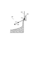
[0008]図1は、一部のCVDプロセスと関連した潜在的なギャップ充填制限を図示するための、異なる堆積ステージの酸化シリコン膜の概略断面図を提供する。ギャップ充填の問題が、この問題をよりよく図示するためにいくらか誇張された形態で図示されている。図1の上部は、水平表面122を有する2つの隣接部材124および128によってギャップ120が定義されており、この水平表面は132で記されているギャップの底部にある初期構造104を示している。構造108、つまり上部から図面の第2の部分に示されているように、従来のHDP−CVD酸化シリコン堆積プロセスは、ギャップ120の底部の水平表面132と、部材124および128上の水平表面122への直接堆積をもたらす。しかし、これはまた、成長に伴って酸化シリコン膜からスパッタリングされた材料の再結合ゆえに、ギャップ120の側壁140上への(「再堆積」と称される)間接堆積をもたらす。特定の幅の狭い高アスペクト比の用途において、酸化シリコン膜の継続的成長は、側壁の下部に横方向に膜が成長するレートを超える成長レートで相互に成長する側壁140の上部セクションへの形成136をもたらす。この傾向は構造108および112に示されており、構造116における最終結果は膜内の間隙144の形成である。間隙を形成する可能性は、再堆積のレートおよび特徴に直接関連している。
[0008] FIG. 1 provides schematic cross-sectional views of silicon oxide films at different deposition stages to illustrate potential gap fill limitations associated with some CVD processes. The gap filling problem is illustrated in some exaggerated form to better illustrate this problem. The upper portion of FIG. 1 defines a
[0009]従って、ギャップ充填技術を改良する一般的な必要性が当業界に存在する。 [0009] Accordingly, there is a general need in the art to improve gap filling techniques.
[0010]本発明の実施形態は、複数の基板上に膜を堆積する方法を提供する。第1のセットの実施形態では、処理チャンバが、シーズン前駆体流を該処理チャンバに提供することによってシーズニングされる。高密度プラズマが、該処理チャンバの上部にソース電力の70%を超えて分布されている少なくとも7500Wのソース電力を印加することによって該シーズン前駆体から形成される。少なくとも5000Åの厚さを有するシーズン層が該高密度プラズマを使用して1つのポイントに堆積される。該複数の基板の各々は該処理チャンバに順次移送されて、エッチングを含むプロセスを該複数の基板の該各々に実行する。該処理チャンバは、該複数の基板の該各々の順次移送の間に洗浄される。 [0010] Embodiments of the invention provide a method of depositing a film on a plurality of substrates. In a first set of embodiments, the processing chamber is seasoned by providing a season precursor stream to the processing chamber. A high density plasma is formed from the season precursor by applying a source power of at least 7500 W distributed over 70% of the source power to the top of the processing chamber. A season layer having a thickness of at least 5000 mm is deposited at one point using the high density plasma. Each of the plurality of substrates is sequentially transferred to the processing chamber to perform a process including etching on each of the plurality of substrates. The processing chamber is cleaned during the respective sequential transfer of the plurality of substrates.
[0011]異なる実施形態では、少なくとも5000Åの該厚さは少なくとも7500Åの厚さを備えてもよく、あるいは少なくとも10,000Åの厚さを備えてもよい。該シーズン前駆体流は、SiH4などのシリコン含有ガス流およびO2などの酸素含有ガス流として提供されてもよい。該酸素含有ガスの該流量は該シリコン含有ガスの流量未満であってもよく、あるいは、異なる実施形態では該シリコン含有ガスの流量の0.8未満であってもよい。一部の例では、該シリコン含有ガスおよび該酸素含有ガスに対して非反応性のガス流は、場合によっては200sccm未満の流量で付加的に提供されることもある。 [0011] In different embodiments, the thickness of at least 5000 mm may comprise a thickness of at least 7500 mm, or may comprise a thickness of at least 10,000 mm. The season precursor stream may be provided as a silicon-containing gas stream such as SiH 4 and an oxygen-containing gas stream such as O 2 . The flow rate of the oxygen-containing gas may be less than the flow rate of the silicon-containing gas, or in a different embodiment, less than 0.8 of the flow rate of the silicon-containing gas. In some examples, a gas flow that is non-reactive with the silicon-containing gas and the oxygen-containing gas may optionally be additionally provided at a flow rate of less than 200 sccm.
[0012]第2のセットの実施形態では、処理チャンバがシーズニングされて、該複数の基板の各々が該処理チャンバに順次移送されて、エッチングを含むプロセスを該複数の基板の該各々に実行する。該処理チャンバは、該処理チャンバの部分的洗浄を実行してから、該処理チャンバを加熱し、その後該処理チャンバの該洗浄を完了させることによって、該複数の基板の該各々の順次移送の間に洗浄される。 [0012] In a second set of embodiments, the processing chamber is seasoned and each of the plurality of substrates is sequentially transferred to the processing chamber to perform a process including etching on each of the plurality of substrates. . The processing chamber performs a partial cleaning of the processing chamber and then heats the processing chamber and then completes the cleaning of the processing chamber during each sequential transfer of the plurality of substrates. To be washed.
[0013]該処理チャンバの該部分的洗浄を実行するステップおよび該処理チャンバの該洗浄を完了するステップの各々は、ハロゲン前駆体を該処理チャンバに流す工程と、該ハロゲン前駆体から高密度プラズマを形成する工程とを備えてもよい。適切なハロゲン前駆体の一例はF2である。該部分的洗浄は、該洗浄のエンドポイントの75%を超えて実行されてもよい。該処理チャンバは、該処理チャンバに熱ガスを流して、該熱ガスから高密度プラズマを形成することによって加熱されてもよい。熱ガスの例は、とりわけO2、ArおよびHeを含んでいる。該高密度プラズマは、上部ソースと側部ソースの間におよそ等しく分布してソース電力を印加することによって該熱ガスから形成されてもよい。 [0013] Each of performing the partial cleaning of the processing chamber and completing the cleaning of the processing chamber includes flowing a halogen precursor into the processing chamber, and a high density plasma from the halogen precursor. Forming a step. An example of a suitable halogen precursor is F 2. The partial cleaning may be performed over 75% of the cleaning endpoint. The processing chamber may be heated by flowing a hot gas through the processing chamber to form a high density plasma from the hot gas. Examples of hot gases include O 2 , Ar and He, among others. The high density plasma may be formed from the hot gas by applying source power approximately equally distributed between the top and side sources.
[0014]本発明の性質および利点についてのさらなる理解は、明細書の残りの部分および図面を参照して実現可能である。 [0014] A further understanding of the nature and advantages of the present invention may be realized by reference to the remaining portions of the specification and the drawings.
[0024]本発明の実施形態は、エッチングステップを組み込む、基板上に膜を堆積する方法を目的としている。本発明の具体的な例示的用途において、酸化シリコン層を堆積して、高密度プラズマCVDプロセスを使用して基板の表面のギャップを充填する方法が提供されている。本発明の技術に従って堆積された酸化シリコン膜は優れたギャップ充填性能を有しており、また、例えばシャロートレンチ分離(「STI」)構造に生じるギャップを充填することができる。本発明のこの方法で堆積された膜は従って、約45nm以下の部材サイズを有する回路を含む多様な集積回路の製作での使用に適している。 [0024] Embodiments of the present invention are directed to a method of depositing a film on a substrate that incorporates an etching step. In a specific exemplary application of the present invention, a method is provided for depositing a silicon oxide layer and filling a gap in the surface of a substrate using a high density plasma CVD process. Silicon oxide films deposited according to the techniques of the present invention have excellent gap fill performance and can fill gaps that occur, for example, in shallow trench isolation (“STI”) structures. Films deposited by this method of the present invention are therefore suitable for use in the fabrication of a variety of integrated circuits, including circuits having a member size of about 45 nm or less.
[0025]このような堆積方法についての研究の一部として本発明者らによってなされた発見は、より多くの基板が処理されると、この方法のエッチング部分でのエッチングレートが減少するというシステム傾向があるということである。この「エッチングレートドリフト」は、各基板のプロセス条件が実質的に同じ場合でも生じる。 [0025] The discovery made by the inventors as part of research on such deposition methods is a system trend that the etch rate in the etched portion of the method decreases as more substrates are processed. Is that there is. This “etching rate drift” occurs even when the process conditions of each substrate are substantially the same.
[0026]本発明の実施形態に従って充填可能な構造のタイプが図2に図示されており、これは未完の集積回路200の簡略断面図を提供している。この集積回路は、複数のSTI構造を含む基板204に形成され、この構造の各々は通常、基板204の表面に薄いパッド酸化膜層220を形成してから、パッド酸化膜層220上に窒化シリコン層216を形成することによって作成される。窒化膜および酸化膜の層は次いで標準フォトリソグラフィ技術を使用してパターニングされ、トレンチ224は窒化膜/酸化膜スタックを介して基板204にエッチングされる。図2は、集積回路が、トランジスタや他のアクティブデバイスで比較的緊密にパックされているエリア208を備えてもよく、また、相対的に分離されているオープンエリア212を備えてもよいことを示している。オープンエリア212におけるアクティブデバイスは、緊密パックエリア208における分離の1倍以上相互に分離可能であるが、本明細書に使用されているように、「オープンエリア」は、ギャップが「緊密エリア」のギャップの幅の少なくとも5倍の幅を有しているエリアであるとみなされる。
[0026] A type of structure that can be filled in accordance with an embodiment of the present invention is illustrated in FIG. 2, which provides a simplified cross-sectional view of an incomplete
[0027]本発明の実施形態は、良好なギャップ充填特性を有する堆積プロセスを使用して二酸化シリコンなどの絶縁性材料によってトレンチ224を充填する方法を提供する。一部の例では、ギャップ充填プロセスの前に、初期ライニング層がイン・シトゥーストリーム発生(「ISSG」)や他の熱酸化膜層、おそらく窒化シリコン層として基板に堆積される。トレンチ224を充填する前にこのようなライナーを堆積することの利点は適切なコーナー丸みを提供することであり、これは、形成されているトランジスタの早期ゲート絶縁破壊などの効果を回避することを目的とすることもある。
[0027] Embodiments of the present invention provide a method of filling
[0028]ここで使用されているように、高密度プラズマプロセスは、同時堆積およびスパッタリングコンポーネントを含み、且つ約1011イオン/cm3以上のイオン密度を有するプラズマを採用するプラズマCVDプロセスである。高密度プラズマの堆積およびスパッタリング特徴の組み合わせの相対的レベルは、ガス状混合物を提供するために使用される流量、プラズマを維持するのに適用されるソース電力レベル、および基板に印加されるバイアス電力などの要因に左右されることがある。このような要因の組み合わせは便宜的に、プロセスを特徴付けるためにD/Sと表記されることもある「堆積/スパッタ比」によって定量化可能である。 [0028] As used herein, a high density plasma process is a plasma CVD process that employs a plasma that includes co-deposition and sputtering components and has an ion density of about 10 11 ions / cm 3 or greater. The relative levels of the combination of high density plasma deposition and sputtering characteristics are the flow rate used to provide the gaseous mixture, the source power level applied to maintain the plasma, and the bias power applied to the substrate. It may be influenced by factors such as. For convenience, this combination of factors can be quantified by the “deposition / sputter ratio”, sometimes referred to as D / S, to characterize the process.
D/S≡(正味堆積レート)+(ブランケットスパッタリングレート)/(ブランケットスパッタリングレート)
堆積/スパッタ比は堆積の増大に伴って増大し、スパッタリングの増大に伴って減少する。D/Sの定義で使用されているように、「正味堆積レート」とは、堆積およびスパッタリングが同時に生じている場合に測定される堆積レートのことである。「ブランケットスパッタレート」は、堆積ガスなしでプロセスレシピが運用される場合に測定されるスパッタレートであり、プロセスチャンバ内の圧力は、堆積時の圧力、およびブランケット熱酸化膜で測定されたスパッタレートに調整される。
D / S≡ (Net deposition rate) + (Blanket sputtering rate) / (Blanket sputtering rate)
The deposition / sputter ratio increases with increasing deposition and decreases with increasing sputtering. As used in the definition of D / S, “net deposition rate” is the deposition rate measured when deposition and sputtering occur simultaneously. “Blanket Sputter Rate” is a sputter rate measured when the process recipe is operated without a deposition gas, and the pressure in the process chamber is the pressure during deposition and the sputter rate measured with a blanket thermal oxide film. Adjusted to
[0029]他の同等の手段も、当業者には既知であるように、HDPプロセスの相対的堆積およびスパッタリング寄与を定量化するために使用可能である。共通の代替比は「エッチング/堆積比」、
E/D≡(ソースのみの堆積レート)−(正味堆積レート)/(ソースのみの堆積レート)
であり、これはスパッタリングの増大に伴って増大し、堆積の増大に伴って減少する。E/Dの定義で使用されているように、「正味堆積レート」はまた、堆積およびスパッタリングが同時に生じている場合に測定された堆積レートのことをいう。「ソースのみの堆積レート」は、しかしながら、スパッタリングなしでプロセスレシピが運用される場合に測定される堆積レートのことである。本発明の実施形態はD/S比に関してここでは説明されている。D/SおよびE/Dは正確な逆数ではないが、これらは逆相関しており、両者間の変換は当業者に理解される。
[0029] Other equivalent means can also be used to quantify the relative deposition and sputtering contributions of the HDP process, as is known to those skilled in the art. Common alternative ratio is “etch / deposition ratio”
E / D≡ (source-only deposition rate) − (net deposition rate) / (source-only deposition rate)
Which increases with increasing sputtering and decreases with increasing deposition. As used in the definition of E / D, “net deposition rate” also refers to the deposition rate measured when deposition and sputtering occur simultaneously. “Source only deposition rate”, however, refers to the deposition rate measured when the process recipe is operated without sputtering. Embodiments of the present invention are described herein with respect to the D / S ratio. Although D / S and E / D are not exact reciprocals, they are inversely correlated and conversion between them will be understood by those skilled in the art.
[0030]HDP−CVDプロセスにおける所与のステップの所望のD/S比は概して、前駆体ガス流、場合によってはスパッタリング剤としても作用可能なフルーエントガス流を含むことによって達成される。前駆体ガスが備える要素は反応して所望の組成を具備する膜を形成する。例えば、酸化シリコン膜を堆積するには、前駆体ガスは、シランSiH4などのシリコン含有ガスおよび酸素分子O2などの酸化ガス反応剤を含むことがある。ドーパントが、例えば膜をフッ素化するためのSiF4の流れを含み、膜をリン化するためのPH3の流れを含み、膜をホウ素化するためのB2H6の流れ含み、膜を窒化するためのN2の流れを含むことによって、所望のドーパントを具備する前駆体ガスを含むことによって膜に添加されてもよい。フルーエントガス(fluent gas)には、H2の流れ、あるいは、Heの流れや、Ne、ArまたはXeなどのより重い不活性ガス流をも含む不活性ガス流が提供されることがある。異なるフルーエントガスによって提供されるスパッタリングレベルはガスの原子質量(あるいは、H2の場合は分子質量)に直接関連しており、H2はHeよりかなり少ないスパッタリングを生成する。本発明の実施形態は概して、5amu未満の平均分子質量を有するフルーエントガス流を提供する。これは、略純H2の流れや略純Heの流れによる単一の低質量ガス流を使用して達成される。代替的に、例えば、HDP−CVDプロセスチャンバで混合するH2の流れおよびHeの流れの両方を提供することによって複数のガス流が提供されることもある。代替的に、このガスは、H2/Heの流れが混合状態でプロセスチャンバに提供されるように事前混合されてもよい。より高い質量のガスの個別流を提供したり、より高い質量のガスを事前混合物に含めたりすることもまた可能であり、事前混合物の相対的な流量および/または濃度は5amu未満の平均分子質量を維持するように選択される。 [0030] The desired D / S ratio for a given step in the HDP-CVD process is generally achieved by including a precursor gas stream, optionally a fluent gas stream that can also act as a sputtering agent. The elements provided in the precursor gas react to form a film having the desired composition. For example, to deposit a silicon oxide film, the precursor gas may include a silicon-containing gas such as silane SiH 4 and an oxidizing gas reactant such as oxygen molecule O 2 . The dopant includes, for example, a stream of SiF 4 for fluorinating the film, a stream of PH 3 for phosphating the film, a stream of B 2 H 6 for boronating the film, and nitriding the film by including a flow of N 2 for, it may be added to the film by including a precursor gas having a desired dopant. Flu in entry gas (fluent gas) are flow H 2, or, He flow and, Ne, may be an inert gas stream is provided that also includes a heavier inert gas such as Ar or Xe. The level of sputtering provided by the different fluent gases is atomic mass (or, in the case of H 2 molecules by mass) are directly related to, H 2 producing even less sputtering than He. Embodiments of the present invention generally provide a fluent gas stream having an average molecular mass of less than 5 amu. This is accomplished using a single low mass gas flow with a substantially pure H 2 flow or a substantially pure He flow. Alternatively, for example, sometimes a plurality of gas streams are provided by providing both a flow of which mix in the HDP-CVD process chamber of H 2 flow and He. Alternatively, the gas may be premixed so that a flow of H 2 / the He is provided in a mixed state to the process chamber. It is also possible to provide a separate stream of higher mass gas or to include higher mass gas in the premix, the relative flow rate and / or concentration of the premix having an average molecular mass of less than 5 amu Selected to maintain.
[0031]高アスペクト比構造において、比較的高流量の低質量フルーエントガスの使用は概して、Arなどのフルーエントガスのより従来型の使用と比較してギャップ充填性能を改良することが分かっている。これは、フルーエントガスとしてHeやH2を使用して達成される再堆積の削減の結果であると思われるため、ギャップの閉鎖はよりゆっくりと生じることになる。しかしこのような低質量フルーエントガスの使用によっても、堆積時のコーナークリッピングの危険性がある。この効果は図3Aおよび3Bを参照して理解可能であり、この図面は、それぞれ緊密パックエリアのギャップおよびオープンエリアのギャップに対するHDPプロセスのスパッタリングコンポーネントの効果を示している。 [0031] In high aspect ratio structures, it has been found that the use of a relatively high flow, low mass fluent gas generally improves the gap fill performance compared to the more conventional use of a fluent gas such as Ar. Since this appears to be the result of the reduction in redeposition achieved using He or H 2 as the fluent gas, the gap closure will occur more slowly. However, the use of such a low-mass fluent gas also risks corner clipping during deposition. This effect can be understood with reference to FIGS. 3A and 3B, which show the effect of the sputtering component of the HDP process on the tight pack area gap and the open area gap, respectively.
[0032]とりわけ、図3Aのギャップ304は高アスペクト比ギャップであり、HDP−CVDプロセスを使用して堆積された材料は水平表面上に特徴カスプ構造308を形成する。経路316に沿ったプラズマイオンの影響に応答してカスプ308から材料312がスパッタリングされると再堆積が生じる。スパッタリングされた材料312は、ギャップ304の反対側の側壁324に合わさる経路320に従う。この効果は対称的であるため、材料がギャップの左側から右側にスパッタリングされると、材料はまたギャップの右側から左側にスパッタリングされる。材料の再堆積はコーナーのクリッピングをもたらす過剰なスパッタリングを防止する。
[0032] In particular, the
[0033]この対称性は、図3Bに示されているオープンエリア構造330で図示されているように、オープンエリアには存在しない。本例では、堆積は類似のカスプ308’の形成を招くが、材料312’が経路316’に沿ったプラズマイオンの衝突に応答して経路320’に沿ってスパッタリングされる場合、ギャップの反対側は再堆積にはかなり遠いため保護されない。図3Bの構造のコーナーは、ギャップの反対側からスパッタリングされた材料を受け取るという補償効果なく、図3Aの構造のコーナーと同じ材料噴出を被っている。結果として、コーナーをクリッピングして下地構造にダメージを与えることのリスクが増大する。
[0033] This symmetry does not exist in the open area, as illustrated by the
[0034]本発明の方法は図4Aの流れ図に要約されており、この図面はこのような方法の概略を提供する。これらの方法は複数の基板の運用に適用され、プロセスは共通の処理チャンバにおいて基板の各々に実行される。この方法は、処理チャンバをシーズニングすることによって、つまり処理チャンバの内部構造を材料によってコーティングすることによってブロック402から開始するが、この材料の一例はSiO2を備えている。ブロック404において、基板が処理チャンバに移送されるためこのプロセスはブロック406で当該基板に実行可能である。このプロセスは、プロセス適用の全結果が材料の正味堆積であっても、相当のエッチングを含んでいる。ブロック410において、基板は処理チャンバ外に移送され、このチャンバはブロック412で洗浄される。
[0034] The method of the present invention is summarized in the flow diagram of FIG. 4A, which provides an overview of such a method. These methods apply to the operation of multiple substrates, and the process is performed on each of the substrates in a common processing chamber. This method, by seasoning the processing chamber, i.e. it begins at
[0035]ブロック414で、基板運用全体が完了されているか否かのチェックがなされる。通常の基板運用は5つの基板を含むことがあるが、異なる具体的な実施形態で使用される基板はより多数または少数であってもよい。基板運用が完了していない場合、運用における次の基板がブロック404で処理チャンバに移送され、この方法はこの次の基板について反復される。基板運用全体が完了されると、プロセスチャンバは、ブロック406で同じプロセスを使用するか、異なるプロセスを使用して、もう1つの基板運用の準備としてブロック402で再度シーズニング可能である。
[0035] At block 414, a check is made whether the entire board operation is complete. A normal substrate operation may include five substrates, although more or fewer substrates may be used in different specific embodiments. If the substrate operation has not been completed, the next substrate in operation is transferred to the processing chamber at
[0036]図4Bは、ブロック406で使用可能なプロセスの詳細を提供する。本例では、堆積/エッチング/堆積プロセスを使用して基板上に堆積が達成されるが、本発明の方法は、かなりのエッチングコンポーネントを有する他のタイプのプロセスに概して適用可能である。基板は通常、200mmまたは300mm直径ウェーハなどの半導体ウェーハである。
[0036] FIG. 4B provides details of the processes available at
[0037]シリコン前駆体流、酸素前駆体流およびフルーエントガス流を含む前駆体ガス流がブロック420でチャンバに提供される。表Iは、モノシランSiH4、酸素分子O2およびH2の流れを使用して無ドープケイ酸塩ガラス(「USG」)膜を堆積するための例示的流量を提供するが、ドーパントソースを含む他の前駆体ガスおよび他のフルーエントガスも上記のように使用可能である点が理解されるはずである。 [0037] A precursor gas stream is provided to the chamber at block 420, including a silicon precursor stream, an oxygen precursor stream, and a fluent gas stream. Table I provides exemplary flow rates for depositing undoped silicate glass (“USG”) films using a flow of monosilane SiH 4 , molecular oxygen O 2 and H 2 , but others including dopant sources It should be understood that other precursor gases and other fluent gases can be used as described above.

表が示しているように、前駆体ガスの流量は200mmおよび300mm直径のウェーハについて類似していることもあるが、フルーエントガスの流量は概してより高い。 As the table shows, the precursor gas flow rate may be similar for 200 mm and 300 mm diameter wafers, but the fluent gas flow rate is generally higher.
[0038]高密度プラズマが、エネルギーをチャンバに結合させることによって、ブロック422でガス状流から形成される。高密度プラズマを生成させる共通の技術は、rfエネルギーを誘導的に結合することである。D/S比は、ガスの流量だけでなく、チャンバへの結合エネルギーの電力密度によって、基板に印加可能なバイアスの強度によって、チャンバ内の温度によって、チャンバ内の圧力によって、更に、他のこのような要因によって判断される。ブロック424において膜の初期部分を堆積するためには、このような処理パラメータが、特定の実施形態では、900〜6000Å/分という比較的低い堆積レートを同時に提供しつつ、20を超えるD/S比を提供するように選択可能である。本発明者らは、ギャップ充填特徴は概して低堆積レートおよび高D/S比のこのような組み合わせで改良されることを、極めて小さな部材サイズによって発見した。
[0038] A high density plasma is formed from the gaseous stream at
[0039]堆積の完了後、堆積前駆体流はブロック426で終了され、膜の所望の厚さに達したか否かがブロック428でチェックされる。本発明の実施形態は、エッチングステージによって分離されている少なくとも2つの堆積ステージを含んでおり、また充填されているギャップの具体的な特徴に応じて5〜15個の堆積ステージまたはより多数の堆積ステージをしばしば有する。
[0039] After the deposition is complete, the deposition precursor flow is terminated at
[0040]このプロセスのエッチング段階は、ハロゲン前駆体を流すことによってブロック430から開始可能であるが、この前駆体は通常、NF3やクロロフルオロカーボンなどのフッ素前駆体を備えている。高密度プラズマが、高いソース電力密度を使用してブロック432においてハロゲン前駆体から形成される。一部の実施形態では、ソース電力密度は約80,000〜140,000W/m2であり、これは300mm直径ウェーハの約6000〜10,000Wの総ソース電力、および200mm直径ウェーハの約2500〜4500Wの総ソース電力に対応している。本発明者らは、高いソース電力の使用によって堆積プロファイルは低いソース電力の使用よりも対称性があるものとなることを発見した。一部の実施形態では、総ソース電力は上部ソースおよび側部ソース間に分布されるため、ソース電力の大部分が側部ソースから提供される。例えば、側部ソース電力は上部ソース電力の1〜5倍であってもよく、これは、具体的な実施形態では上部ソース電力の3倍である。
[0040] The etch stage of the process can begin at
[0041]得られるハロゲンプラズマは、堆積膜をエッチングバックするためにブロック434で使用される。エッチング可能な具体的な量の材料は基板構造の具体的構成に比較的左右されるが、エッチングされる材料の量が早期のエッチングサイクルよりも後のエッチングサイクルにおいてのほうが多い場合がある点は概して事実である。これは、堆積およびエッチングステップのシーケンスの結果として基板のトポロジー全体が変化するという事実の一般的結果である。ステップシーケンスによる一般的な傾向は、トポロジーは、サイクルのエッチング段階でより多くのエッチング量に影響を受けやすくなるということである。ブロック436において、ハロゲン前駆体流は終了されるため、プロセスは、ブロック420でシリコン前駆体、酸素前駆体およびフルーエントガス流を再度流すことによって、堆積段階に戻ることができる。
[0041] The resulting halogen plasma is used at
[0042]同一の前駆体が堆積段階の各々で材料堆積に使用され、且つ同一の前駆体がエッチング段階で材料除去に使用されることが概して予想されるが、これは本発明の要件ではない。堆積段階の各々で堆積される材料の量は通常300〜1000Åであり、プロセス全体は、サイクルあたりの堆積量がより多い場合にはより少ないサイクルですむ。各サイクルで300Å堆積する場合、各サイクルで1000Å堆積する場合と同じ量の材料を堆積するためには約6倍のサイクルを使用する必要がある。 [0042] Although it is generally expected that the same precursor will be used for material deposition at each of the deposition stages and the same precursor will be used for material removal at the etching stage, this is not a requirement of the present invention. . The amount of material deposited at each of the deposition stages is typically 300-1000 liters, and the entire process requires fewer cycles with more deposition per cycle. When depositing 300 soot in each cycle, approximately 6 times as many cycles need to be used to deposit the same amount of material as 1000 soot in each cycle.
[0043]図4Cは、一部の実施形態ではブロック402で使用可能なシーズニングプロセスを図示している。シーズニングプロセスは、チャンバ内のシーズニング条件を確立することによってブロック440から開始する。特定の実施形態では、このような条件は24〜65ミリトールのチャンバ圧力を含んでいる。シーズン前駆体流はブロック442で提供される。シーズンがSiO2コーティングを含む実施形態では、前駆体は、シランなどのシリコン含有ガスおよび酸素含有ガスを含むことがある。例えば、シリコン前駆体はSiH4を含むことがあり、酸素前駆体はO2を含むことがある。一部の実施形態では、酸素含有ガスの流量はシリコン含有ガスの流量未満であり、シリコン含有ガスの流量の0.9倍未満のこともあり、シリコン含有ガスの流量の0.8倍未満のこともあり、シリコン含有ガスの流量の0.7倍未満のこともあり、シリコン含有ガスの流量の0.6倍未満のこともあり、あるいはシリコン含有ガスの流量の0.5倍未満のこともある。例えば、SiH4およびO2を使用する一実施形態では、O2の流量は300sccmであり、SiH4の流量は470sccmであり、流量比はおよそ0.65に等しい。ブロック442で提供された流れはまた、He、NeまたはArを使用する実施形態のように非反応性ガスを含むこともある。このような非反応性ガスの流量は通常、スパッタ効果を削減するために200sccm未満であり、0sccmのこともある。
[0043] FIG. 4C illustrates a seasoning process that may be used in
[0044]ブロック444において、高密度プラズマが、上記のように処理チャンバへのエネルギーの結合によってシーズン前駆体から形成される。エネルギーは好ましくは、上部ソース電力の印加によって優先的に結合され、本発明の実施形態は、チャンバの上部に印加されたソース電力の70%超を、チャンバの上部に印加されたソース電力の80%超を、チャンバの上部に印加されたソース電力の90%超を、あるいはチャンバの上部に印加されたソース電力の100%を有する。印加された通常の電力は7500W超であり、一実施形態は、処理チャンバの上部全体に印加されたおよそ9000Wを使用する。
[0044] At
[0045]高密度プラズマは、ブロック446でシーズン層を堆積するために使用される。シーズン層の厚さが不均一である場合がある点は概して想定されているが、一部の実施形態では、あるポイントでは少なくとも5000Åの厚さを有しており、あるポイントでは少なくとも6000Åの厚さを有しており、あるポイントでは少なくとも7500Åの厚さを有しており、あるポイントでは少なくとも10,000Åの厚さを有しており、あるいはあるポイントでは少なくとも12,500Åの厚さを有している。シーズン層の堆積後、シーズン前駆体流はブロック448で停止される。
[0045] A high density plasma is used to deposit the season layer at
[0046]図4Dは、本発明の実施形態に従って図4Aのブロック412においてチャンバを洗浄する方法を図示するフロー図を提供する。この洗浄方法は、2つの洗浄ステージ間で実行される加熱プロセスを具備する2ステージ洗浄を備えている。
[0046] FIG. 4D provides a flow diagram illustrating a method of cleaning the chamber at
[0047]従って、ブロック460において、F2などのハロゲン前駆体が、基板が処理された後に処理チャンバに流される。高密度プラズマがブロック46においてハロゲン前駆体によって形成され、部分的洗浄が高密度プラズマを使用してブロック464で実行される。部分的洗浄は一部の実施形態では、プロセスのエンドポイントの75%を超えて実行されることもある。
[0047] Accordingly, at
[0048]第1の洗浄ステージが完了された後、ハロゲン前駆体流はブロック466で停止される。この流れは、ブロック468において熱ガス流と置換され、これによって加熱プラズマがブロック470において形成される。例証としてのみ、熱ガスは異なる実施形態ではO2、Arおよび/またはHeを含むことがあり、12,000Wの例示的ソース電力は、30〜120秒間に上部および側部の等しい分布で印加される。この中間加熱は、洗浄中に生じるチャンバの一般的な冷却を打ち消すように作用する。
[0048] After the first cleaning stage is completed, the halogen precursor flow is stopped at
[0049]熱ガス流がブロック472で停止された後、ハロゲン前駆体流はブロック474で再開されることがあり、またチャンバ洗浄を完了させるために使用される高密度プラズマがブロック475で形成される。
[0049] After the hot gas flow is stopped at
[0050]本発明者らは、カリフォルニア州サンタクララのAPPLIED MATERIALS,INC.によって製造されているULTIMA(商標)によって本発明の実施形態を実現しており、これに関する一般的説明は、Fred C.Redeker、Farhad Moghadam、Hirogi Hanawa、Tetsuya Ishikawa、Dan Maydan、Shijian Li、Brian Lue、Robert Steger、Yaxin Wang、 Manus WongおよびAshok Sinhaによって1996年7月15日に出願された共に譲渡された米国特許第6,170,428号「SYMMETRIC TUNABLE INDUCTIVELY COUPLED HDP−CVD REACTOR」に提供されており、この開示全体は参照して本明細書に組み込まれている。このシステムの概要は以下の図5Aおよび5Bと関連して提供されている。図5Aは、一実施形態のこのようなHDP−CVDシステム510の構造を概略的に図示している。システム510はチャンバ513と、真空システム570と、ソースプラズマシステム580Aと、バイアスプラズマシステム580Bと、ガス送出システム533と、遠隔プラズマ洗浄システム550と、を含んでいる。
[0050] The inventors have reported in APPLIED MATERIALS, INC. Of Santa Clara, California. An embodiment of the present invention is realized by ULTIMA ™ manufactured by U.S. Pat. Redeker, Farhad Mohdamam, Hirogi Hanawa, Tetsuya Ishikawa, Dan Maydan, Shijian Li, Brian Lue, Robert Steger, Yaxin Wang, on March 15 170, 428, “SYMMETRIC TUNABLE INDUCTIVELY COUPLED HDP-CVD REACTOR”, the entire disclosure of which is incorporated herein by reference. An overview of this system is provided in connection with FIGS. 5A and 5B below. FIG. 5A schematically illustrates the structure of such an HDP-
[0051]チャンバ513の上部はドーム514を含んでおり、これは酸化アルミニウムや窒化アルミニウムなどのセラミック誘電材料からなる。ドーム514はプラズマ処理領域516の上部境界を画成する。プラズマ処理領域516は、基板517の上部表面および基板サポート部材518によって底部に境界設定されている。
[0051] The top of the
[0052]ヒータープレート523および冷却プレート524はドーム514の上にあり、これに熱的に結合されている。ヒータープレート523および冷却プレート524によってドーム温度のコントロールは約100℃〜200℃の範囲の±10℃になる。これによって種々のプロセスに対してドーム温度を最適化することができる。例えば、堆積プロセスよりも洗浄またはエッチングプロセスのほうがより高い温度でドームを維持することが望ましい。ドーム温度の正確なコントロールはまた、チャンバの剥がれや粒子カウントを削減し、且つ堆積層と基板間の接着を改良する。
[0052] The
[0053]チャンバ513の下部は本体部材522を含んでおり、これはチャンバを真空システムに接合している。基板サポート部材518のベース部分521は本体部材522に搭載されており、且つこれとの連続内部表面を形成する。基板は、チャンバ513の側面の挿入/除去開口(図示せず)を介してロボットブレード(図示せず)によってチャンバ513の内外に移送される。リフトピン(図示せず)は、モーター(これも図示せず)のコントロールに基づいて上昇、次いで降下させられ、上部ローディング位置557のロボットブレードから、基板が基板サポート部材518の基板受け取り部分519に配置されている下部処理位置556に基板を移動させる。基板受け取り部分519は、基板処理中に基板サポート部材518に基板を固定する静電チャック520を含んでいる。好ましい実施形態では、基板サポート部材518は酸化アルミニウムやアルミニウムセラミック材料から作られる。
[0053] The lower portion of
[0054]真空システム570はスロットル本体525を含んでおり、これはツインブレードスロットルバルブ526を収容しており、またゲートバルブ527およびターボ分子ポンプ528に取り付けられている。スロットル本体525はガス流への障害を最小にし、対称ポンピングを可能にする点が注目されるべきである。ゲートバルブ527はポンプ528をスロットル本体525から分離可能であり、また、スロットルバルブ526が完全に開放されている場合に排出流容量を制約することによってチャンバ圧力をコントロール可能である。スロットルバルブ、ゲートバルブおよびターボ分子ポンプの配列は、最大約1ミリトール〜約2トールのチャンバ圧力の正確且つ安定したコントロールを可能にする。
[0054] The
[0055]ソースプラズマシステム580Aは、ドーム514に搭載されている上部コイル529および側部コイル530を含んでいる。対称接地シールド(図示せず)はコイル間の電気結合を削減する。上部コイル529は上部ソースRF(SRF)生成器531Aによって電源投入されるが、側部コイル530は側部SRF生成器531Bによって電源投入され、コイルごとの動作の独立電力レベルおよび周波数を可能にする。このデュアルコイル方式はチャンバ513における放射イオン密度のコントロールを可能にすることによって、プラズマ均一性を改良することができる。側部コイル530および上部コイル529は通常誘導駆動され、これは相補電極を必要としない。具体的な実施形態では、上部ソースRF生成器531Aは、普通は2MHzで最大2,500ワットのRF電力を提供し、側部ソースRF生成器531Bは、普通は2MHzで最大5,000ワットのRF電力を提供する。上部および側部のRF生成器の動作周波数は、プラズマ生成効率を改良するために、名目動作周波数(例えば、それぞれ1.7〜1.9MHzおよび1.9〜2.1MHz)からオフセットされることもある。
[0055] The
[0056]バイアスプラズマシステム580BはバイアスRF(「BRF」)生成器531Cおよびバイアス整合ネットワーク532Cを含んでいる。バイアスプラズマシステム580Bは基板部分517を本体部材522に容量結合させ、これは相補電極として作用する。バイアスプラズマシステム580Bは、ソースプラズマシステム580Aによって作成されたプラズマ種(例えば、イオン)の基板表面への移送を高める役目をする。具体的な実施形態では、バイアスRF生成器は、さらに後述されるように、5MHz未満の周波数で最大10,000ワットのRF電力を提供する。
[0056] The
[0057]RF生成器531Aおよび531Bは、ディジタルコントロール合成器を含んでおり、約1.8〜約2.1MHzの周波数範囲で動作する。各生成器は、当業者によって理解されるように、チャンバおよびコイルから生成器に反射し返された電力を測定し、且つ動作周波数を調整して最低反射電力を取得するRFコントロール回路(図示せず)を含んでいる。RF生成器は通常、50オームの特徴インピーダンスの負荷で動作するように設計されている。RF電力は、生成器とは異なる特徴インピーダンスを有する負荷から反射されることがある。これは、負荷に移送される電力を削減可能である。加えて、負荷から生成器に反射し返された電力はオーバーロードして、生成器にダメージを与えることもある。プラズマのインピーダンスは、とりわけプラズマイオン密度に応じて5オーム未満から900オームを超えた範囲に及ぶこともあるため、また反射電力は周波数の関数であってもよいため、反射電力に従った生成器周波数の調整は、RF生成器からプラズマに移送される電力を増大させ、生成器を保護する。反射電力を削減し、且つ効率を改良するもう1つの方法は整合ネットワークによるものである。
[0057]
[0058]整合ネットワーク532Aおよび532Bは生成器531Aおよび531Bの出力インピーダンスをそれぞれのコイル529および530に整合させる。RFコントロール回路は、負荷の変化に伴って、整合ネットワーク内のコンデンサの値を変更して生成器を負荷に整合させることによって両方の整合ネットワークをチューニング可能である。RFコントロール回路は、負荷から生成器に反射し返された電力が特定の制限を越える場合に整合ネットワークをチューニング可能である。一定の整合を提供し、且つ効果的に、RFコントロール回路が整合ネットワークをチューニングできないようにする方法は、反射電力の予想値よりも高く反射電力限度を設定することである。これは、整合ネットワークを最新の条件で一定に保持することによって、いくつかの条件下でプラズマを安定させる助けとなることがある。
[0058]
[0059]他の手段もまたプラズマを安定させる助けとなることがある。例えば、RFコントロール回路は、負荷(プラズマ)に送出された電力を判断するために使用可能であり、また、生成器出力電力を増減させて、層の堆積中に送出電力を略一定に維持してもよい。 [0059] Other means may also help stabilize the plasma. For example, an RF control circuit can be used to determine the power delivered to the load (plasma), and the generator output power can be increased or decreased to keep the delivered power approximately constant during layer deposition. May be.
[0060]ガス送出システム533は、ガス送出ライン538(このうちのいくつかのみが示されている)を介して基板を処理するための複数のソース534A〜534Eのチャンバからガスを提供する。当業者に理解されるように、ソース534A〜534Eに使用される実際のソースと、チャンバ513への送出ライン538の実際の接続は、チャンバ513内で実行される堆積および洗浄プロセスに応じて変化する。ガスは、ガスリング537および/または上部ノズル545を介してチャンバ513に導入される。図5Bは、ガスリング537のさらなる詳細を示す、チャンバ513の簡略部分断面図である。
[0060] The
[0061]一実施形態では、第1および第2のガス源534Aおよび534Bと、第1および第2のガス流コントローラー535A’および535B’は、ガス送出ライン538(このうちのいくつかのみが示されている)を介してガスリング537のリングプレナム536にガスを提供する。ガスリング537は、基板に均一なガス流を提供する複数のソースガスノズル539(このうちの1つのみが図示目的で示されている)を有している。ノズル長およびノズル角度は、個別チャンバ内の具体的プロセスの均一性プロファイルおよびガス利用効率の調整を可能にするように変更されてもよい。好ましい実施形態では、ガスリング537は、酸化アルミニウムセラミックからなる12個のソースガスノズルを有している。
[0061] In one embodiment, the first and
[0062]ガスリング537はまた複数の酸化剤ガスノズル540(このうちの1つのみが示されている)を有しており、これらは、好ましい実施形態ではソースガスノズル539と同一平面にあり、且つこれより短く、また一実施形態では本体プレナム541からガスを受け取る。一部の実施形態では、ガスをチャンバ513に注入する前にソースガスおよび酸化剤ガスを混合しないことが望ましい。他の実施形態では、酸化剤ガスおよびソースガスは、本体プレナム541とガスリングプレナム536間にアパーチャー(図示せず)を提供することによって、ガスをチャンバ513に注入する前に混合されてもよい。一実施形態では、第3、第4および第5のガス源534C、534Dおよび534D’と、第3および第4のガス流コントローラー535Cおよび535D’はガス送出ライン538を介して本体プレナムにガスを提供する。543Bなどの追加バルブ(他のバルブは図示せず)は、流れコントローラーからチャンバへのガスをシャットオフ可能である。本発明の特定の実施形態を実現する際、ガス源534AはシランSiH4ソースを備えており、ガス源534Bは酸素分子O2ソースを備えており、ガス源534CはシランSiH4ソースを備えており、ガス源534DはヘリウムHeソースを備えており、ガス源534D’は水素分子H2ソースを備えている。
[0062] The
[0063]可燃、有毒または腐食ガスが使用される実施形態では、堆積後にガス送出ラインに残っているガスを排除することが望ましい。これは、例えば、チャンバ513を送出ライン538Aから分離し、且つ送出ライン538Aを真空フォーライン(foreline)544に換気するために、バルブ543Bなどの3方向バルブを使用して達成可能である。図5Aに示されているように、543Aおよび543Cなどの他の類似のバルブが他のガス送出ラインに組み込まれてもよい。このような3方向バルブは、(3方向バルブとチャンバ間の)未換気ガス送出ラインの容積を最小化するために、可能な限りチャンバ513の近くに配置されてもよい。加えて、2方向(オン−オフ)バルブ(図示せず)は、質量流コントローラー(「MFC」)とチャンバ間、あるいはガス源とMFC間に配置されてもよい。
[0063] In embodiments where flammable, toxic or corrosive gases are used, it is desirable to eliminate gas remaining in the gas delivery line after deposition. This can be accomplished, for example, using a three-way valve, such as
[0064]図5Aを再度参照すると、チャンバ513はまた上部ノズル545および上部通気孔546を有している。上部ノズル545および上部通気孔546はガスの上部および側部の流れの独立コントロールを可能にし、これは膜の均一性を改良し、且つ膜の堆積およびドーピングパラメータの精密調整を可能にする。上部通気孔546は上部ノズル545周辺の環状開口である。一実施形態では、第1のガス源534Aはソースガスノズル539および上部ノズル545を供給する。ソースノズルMFC535A’はソースガスノズル539に送出されるガス量をコントロールし、上部ノズルMFC535Aは上部ガスノズル545に送出されるガス量をコントロールする。同様に、2つのMFC535Bおよび535B’は、ガス源534Bなどの単一の酸素ソースから上部通気孔546および酸化剤ガスノズル540の両方への酸素流をコントロールするために使用可能である。一部の実施形態では、酸素は側部ノズルからはチャンバに供給されない。上部ノズル545および上部通気孔546に供給されたガスは、ガスをチャンバ513に流す前に別個に維持されてもよく、あるいはガスは、チャンバ513に流れる前に上部プレナム548で混合されてもよい。別個のソースの同一ガスが、チャンバの種々の部分に供給するために使用可能である。
[0064] Referring again to FIG. 5A, the
[0065]遠隔マイクロ波生成プラズマ洗浄システム550が、チャンバコンポーネントからの堆積残渣を定期的に洗浄するために提供される。洗浄システムは、反応器キャビティ553の洗浄ガス源534E(例えば、フッ素分子、三フッ化窒素、他のフッ化炭素や同等物)からプラズマを作成する遠隔マイクロ波生成器551を含んでいる。このプラズマから得られる反応種は、アプリケーターチューブ555を介して洗浄ガスフィードポート443を通ってチャンバ513に搬送される。洗浄プラズマ(例えば、キャビティ553およびアプリケーターチューブ555)を含有するために使用される材料は、プラズマによる攻撃に耐性がなければならない。反応器キャビティ553とフィードポート554間の距離は可能な限り短く維持されなければならないが、これは、所望のプラズマ種の濃度は反応器キャビティ553からの距離に伴って低下することがあるためである。遠隔キャビティでの洗浄プラズマの生成は効率的なマイクロ波生成器の使用を可能にし、また、イン・シトゥーで形成されたプラズマに存在しうるグロー放電の温度、放射または衝撃にチャンバコンポーネントをさらさない。結果として、静電チャック520などの比較的感度の高いコンポーネントは、イン・シトゥープラズマ洗浄プロセスで必要とされるように、ダミーウェーハでカバーされたり、他の方法で保護されたりする必要はない。図5Aにおいて、プラズマ洗浄システム550はチャンバ513の上方に配置されて示されているが、他の位置も代替的に使用可能である。
[0065] A remote microwave-generated
[0066]バッフル561が、上部ノズルを介して供給されるソースガス流をチャンバに方向付けし、且つ遠隔生成プラズマの流れを方向付けるために上部ノズルに近接して提供されてもよい。上部ノズル545を介して提供されたソースガスは中央通路562を介してチャンバに方向付けられるのに対して、洗浄ガスフィードポート554を介して提供された遠隔生成プラズマ種はバッフル561によってチャンバ513の側面に方向付けられる。
[0066] A
[0067]当業者は、本発明の精神から逸脱することなく、異なる処理チャンバおよび異なる処理条件について具体的パラメータが変更可能である点を認識する。他の変形例もまた当業者には明らかである。これらの同等物および代替物は本発明の範囲内に含まれることが意図されている。従って、本発明の範囲は上記実施形態に制限されるべきではなく、また以下の請求項によって定義されるべきである。 [0067] Those skilled in the art will recognize that specific parameters can be varied for different processing chambers and different processing conditions without departing from the spirit of the invention. Other variations will also be apparent to those skilled in the art. These equivalents and alternatives are intended to be included within the scope of the present invention. Accordingly, the scope of the invention should not be limited to the above embodiments, but should be defined by the following claims.
104…初期構造、108、112、116…構造、120、304…ギャップ、122…水平表面、124、128…部材、140、324…側壁、200…集積回路、204、517…基板、212…オープンエリア、216…窒化シリコン層、220…パッド酸化膜層、224…トレンチ、304…ギャップ、308…カスプ、312、312’…材料、316、316’、320、320’…経路、324…側壁、510…システム、513…チャンバ、514…ドーム、516…プラズマ処理領域、518…基板サポート部材、519…基板受け取り部分、520…静電チャック、521…ベース部分、522…本体部材、523…ヒータープレート、524…冷却プレート、525…スロットル本体、526…スロットルバルブ、527…ゲートバルブ、528…ポンプ、529…上部コイル、530…側部コイル、531A…上部ソースRF生成器、531B…側部SRF生成器、531C…バイアスRF生成器、532A、532B…整合ネットワーク、532C…バイアス整合ネットワーク、533…ガス送出システム、534A〜534E…ガス源、535A’、535B’…ガス流コントローラー、536…リングプレナム、537…ガスリング、538…ガス送出ライン、539…ソースガスノズル、540…酸化剤ガスノズル、541…本体プレナム、543A、543B,543C…バルブ、544…真空フォアライン、545…上部ノズル、546…上部通気孔、548…上部プレナム、550…遠隔プラズマ洗浄システム、551…遠隔マイクロ波生成器、553…キャビティ、554…洗浄ガスフィードポート、555…アプリケーターチューブ、557…上部ローディング位置、561…バッフル、562…中央通路、570…真空システム、580A…ソースプラズマシステム、580B…バイアスプラズマシステム
104: initial structure, 108, 112, 116 ... structure, 120, 304 ... gap, 122 ... horizontal surface, 124, 128 ... member, 140, 324 ... sidewall, 200 ... integrated circuit, 204, 517 ... substrate, 212 ... open Area, 216 ... Silicon nitride layer, 220 ... Pad oxide layer, 224 ... Trench, 304 ... Gap, 308 ... Cusp, 312, 312 '... Material, 316, 316', 320, 320 '... Path, 324 ... Side wall, 510 ... System, 513 ... Chamber, 514 ... Dome, 516 ... Plasma processing region, 518 ... Substrate support member, 519 ... Substrate receiving portion, 520 ... Electrostatic chuck, 521 ... Base portion, 522 ... Body member, 523 ...
Claims (11)
処理チャンバをシーズニングするステップであって、
前記処理チャンバにシーズン前駆体流を提供する工程と、
前記処理チャンバの上部にソース電力の70%を超えて分布されている少なくとも7500Wのソース電力を印加することによって前記シーズン前駆体から高密度プラズマを形成する工程と、
前記高密度プラズマによってあるポイントに少なくとも5000Åの厚さを有するシーズン層を堆積する工程と、を備える前記ステップと、
前記複数の基板の各々を前記処理チャンバに順次移送して、エッチングを含むプロセスを前記複数の基板の前記各々に実行するステップと、
前記複数の基板の前記各々の順次移送の間に前記処理チャンバを洗浄するステップと、を備え、
前記処理チャンバを洗浄するステップが、
ハロゲン前駆体流から高密度プラズマを形成することにより、前記処理チャンバの部分的洗浄を実行する工程と、
この後、前記ハロゲン前駆体流を停止する工程と、
この後、加熱ガスからのプラズマにより前記処理チャンバを加熱する工程と、
この後、前記加熱ガス流を停止する工程と、
この後、ハロゲン前駆体流から高密度プラズマを形成することにより、前記処理チャンバの前記洗浄を完了させる工程と、を備える、方法。 A method of depositing a film on a plurality of substrates, the method comprising:
Seasoning the processing chamber, comprising:
Providing a season precursor stream to the processing chamber;
Forming a high density plasma from the season precursor by applying a source power of at least 7500 W distributed over 70% of the source power to the top of the processing chamber;
Depositing a season layer having a thickness of at least 5000 mm at a point by the high-density plasma; and
Sequentially transferring each of the plurality of substrates to the processing chamber to perform a process including etching on each of the plurality of substrates;
Cleaning the processing chamber during each sequential transfer of the plurality of substrates;
Cleaning the processing chamber comprises:
Performing a partial cleaning of the processing chamber by forming a high density plasma from a halogen precursor stream ;
After this, stopping the halogen precursor flow;
Thereafter, heating the processing chamber with plasma from a heated gas ;
Thereafter, the step of stopping the heated gas flow;
Then completing the cleaning of the processing chamber by forming a high density plasma from a halogen precursor stream .
前記処理チャンバにシリコン含有ガス流を提供することと、
前記処理チャンバに酸素含有ガス流を提供することと、を備える、請求項1に記載の方法。 Providing the season precursor stream to the processing chamber;
Providing a silicon-containing gas stream to the processing chamber;
Providing a flow of oxygen-containing gas to the processing chamber.
処理チャンバをシーズニングするステップと、
前記複数の基板の各々を前記処理チャンバに順次移送して、エッチングを含むプロセスを前記複数の基板の前記各々に実行するステップと、
前記複数の基板の前記各々の順次移送の間に前記処理チャンバを洗浄するステップであって、
ハロゲン前駆体流から高密度プラズマを形成することにより、前記処理チャンバの部分的洗浄を実行する工程と、
この後、前記ハロゲン前駆体流を停止する工程と、
この後、加熱ガスからのプラズマにより前記処理チャンバを加熱する工程と、
この後、前記加熱ガス流を停止する工程と、
この後、ハロゲン前駆体流から高密度プラズマを形成することにより、前記処理チャンバの前記洗浄を完了させる工程と、を備える前記ステップと、を備える方法。 A method for depositing a film on a plurality of substrates, comprising:
Seasoning the processing chamber;
Sequentially transferring each of the plurality of substrates to the processing chamber to perform a process including etching on each of the plurality of substrates;
Cleaning the processing chamber during each sequential transfer of the plurality of substrates,
Performing a partial cleaning of the processing chamber by forming a high density plasma from a halogen precursor stream ;
After this, stopping the halogen precursor flow;
Thereafter, heating the processing chamber with plasma from a heated gas ;
Thereafter, the step of stopping the heated gas flow;
Then completing the cleaning of the processing chamber by forming a high density plasma from a halogen precursor stream .
前記加熱ガスから前記高密度プラズマを形成することが、上部ソースと側部ソース間に等しく分布されたソース電力を印加することを備える、請求項10に記載の方法。 The heated gas comprises a gas selected from the group consisting of O 2 , Ar and He;
Wherein the heating gas to form a high density plasma comprises applying a source power it is equally distributed between the upper and side sources, A method according to claim 10.
Applications Claiming Priority (4)
| Application Number | Priority Date | Filing Date | Title |
|---|---|---|---|
| US97088407P | 2007-09-07 | 2007-09-07 | |
| US60/970,884 | 2007-09-07 | ||
| US12/204,503 | 2008-09-04 | ||
| US12/204,503 US7867921B2 (en) | 2007-09-07 | 2008-09-04 | Reduction of etch-rate drift in HDP processes |
Publications (3)
| Publication Number | Publication Date |
|---|---|
| JP2009111350A JP2009111350A (en) | 2009-05-21 |
| JP2009111350A5 JP2009111350A5 (en) | 2011-10-20 |
| JP5197256B2 true JP5197256B2 (en) | 2013-05-15 |
Family
ID=40130786
Family Applications (1)
| Application Number | Title | Priority Date | Filing Date |
|---|---|---|---|
| JP2008230063A Expired - Fee Related JP5197256B2 (en) | 2007-09-07 | 2008-09-08 | Reduction of etching rate drift in HDP process |
Country Status (6)
| Country | Link |
|---|---|
| US (1) | US7867921B2 (en) |
| EP (1) | EP2034045A3 (en) |
| JP (1) | JP5197256B2 (en) |
| KR (1) | KR101035775B1 (en) |
| SG (1) | SG151185A1 (en) |
| TW (1) | TWI397960B (en) |
Families Citing this family (12)
| Publication number | Priority date | Publication date | Assignee | Title |
|---|---|---|---|---|
| US7972968B2 (en) * | 2008-08-18 | 2011-07-05 | Applied Materials, Inc. | High density plasma gapfill deposition-etch-deposition process etchant |
| KR101794069B1 (en) | 2010-05-26 | 2017-12-04 | 삼성전자주식회사 | equipment for manufacturing semiconductor device and seasoning process optimization method of the same |
| JP5837793B2 (en) | 2010-11-30 | 2015-12-24 | 株式会社日立国際電気 | Substrate processing apparatus, semiconductor device manufacturing method, and baffle structure of substrate processing apparatus |
| JP6060242B2 (en) * | 2010-11-30 | 2017-01-11 | 株式会社日立国際電気 | Substrate processing apparatus, semiconductor device manufacturing method, and baffle structure |
| JP5599350B2 (en) * | 2011-03-29 | 2014-10-01 | 東京エレクトロン株式会社 | Film forming apparatus and film forming method |
| KR20140110080A (en) * | 2012-01-09 | 2014-09-16 | 어플라이드 머티어리얼스, 인코포레이티드 | Method for seasoning uv chamber optical components to avoid degradation |
| US8872339B2 (en) * | 2012-02-10 | 2014-10-28 | Taiwan Semiconductor Manufacturing Company, Ltd. | Semiconductors structure with elements having different widths and methods of making the same |
| TWI522490B (en) * | 2012-05-10 | 2016-02-21 | 應用材料股份有限公司 | Method of depositing a film on a substrate using microwave plasma chemical vapor deposition |
| SG195494A1 (en) * | 2012-05-18 | 2013-12-30 | Novellus Systems Inc | Carbon deposition-etch-ash gap fill process |
| US9018108B2 (en) | 2013-01-25 | 2015-04-28 | Applied Materials, Inc. | Low shrinkage dielectric films |
| DE102015205719B4 (en) * | 2015-03-30 | 2022-08-18 | Siltronic Ag | Process for coating semiconductor wafers |
| KR102601581B1 (en) | 2018-10-31 | 2023-11-14 | 삼성전자주식회사 | Device for providing gas into a plasma chamber and plasma processing device applying thereof |
Family Cites Families (38)
| Publication number | Priority date | Publication date | Assignee | Title |
|---|---|---|---|---|
| US6170428B1 (en) | 1996-07-15 | 2001-01-09 | Applied Materials, Inc. | Symmetric tunable inductively coupled HDP-CVD reactor |
| JP3568749B2 (en) * | 1996-12-17 | 2004-09-22 | 株式会社デンソー | Dry etching method for semiconductor |
| JP2894304B2 (en) * | 1996-12-20 | 1999-05-24 | 日本電気株式会社 | Method for manufacturing semiconductor device |
| US5849092A (en) * | 1997-02-25 | 1998-12-15 | Applied Materials, Inc. | Process for chlorine trifluoride chamber cleaning |
| US6125859A (en) * | 1997-03-05 | 2000-10-03 | Applied Materials, Inc. | Method for improved cleaning of substrate processing systems |
| US6274058B1 (en) * | 1997-07-11 | 2001-08-14 | Applied Materials, Inc. | Remote plasma cleaning method for processing chambers |
| US6071573A (en) | 1997-12-30 | 2000-06-06 | Lam Research Corporation | Process for precoating plasma CVD reactors |
| US6750149B2 (en) | 1998-06-12 | 2004-06-15 | Matsushita Electric Industrial Co., Ltd. | Method of manufacturing electronic device |
| US6143078A (en) * | 1998-11-13 | 2000-11-07 | Applied Materials, Inc. | Gas distribution system for a CVD processing chamber |
| JP2000173932A (en) * | 1998-12-08 | 2000-06-23 | Sony Corp | Method for cleaning reaction furnace |
| US6374831B1 (en) | 1999-02-04 | 2002-04-23 | Applied Materials, Inc. | Accelerated plasma clean |
| KR100448291B1 (en) * | 1999-07-12 | 2004-09-10 | 에이에스엠엘 유에스, 인코포레이티드 | Method and system for in situ cleaning of semiconductor manufacturing equipment using combination chemistries |
| US6274500B1 (en) * | 1999-10-12 | 2001-08-14 | Chartered Semiconductor Manufacturing Ltd. | Single wafer in-situ dry clean and seasoning for plasma etching process |
| US6479098B1 (en) | 2000-12-26 | 2002-11-12 | Taiwan Semiconductor Manufacturing Company | Method to solve particle performance of FSG layer by using UFU season film for FSG process |
| US6584987B1 (en) | 2001-03-16 | 2003-07-01 | Taiwan Semiconductor Manufacturing Company | Method for improved cleaning in HDP-CVD process with reduced NF3 usage |
| DE10130340A1 (en) * | 2001-06-26 | 2003-01-02 | Bhs Corr Masch & Anlagenbau | Web tension control device for corrugated cardboard plant |
| US6846745B1 (en) | 2001-08-03 | 2005-01-25 | Novellus Systems, Inc. | High-density plasma process for filling high aspect ratio structures |
| JP2003077839A (en) | 2001-08-30 | 2003-03-14 | Toshiba Corp | Purging method of semiconductor-manufacturing apparatus and manufacturing method of semiconductor device |
| US6869880B2 (en) | 2002-01-24 | 2005-03-22 | Applied Materials, Inc. | In situ application of etch back for improved deposition into high-aspect-ratio features |
| US6777308B2 (en) | 2002-05-17 | 2004-08-17 | Micron Technology, Inc. | Method of improving HDP fill process |
| TWI235433B (en) | 2002-07-17 | 2005-07-01 | Tokyo Electron Ltd | Oxide film forming method, oxide film forming apparatus and electronic device material |
| US6767836B2 (en) | 2002-09-04 | 2004-07-27 | Asm Japan K.K. | Method of cleaning a CVD reaction chamber using an active oxygen species |
| US7223701B2 (en) | 2002-09-06 | 2007-05-29 | Intel Corporation | In-situ sequential high density plasma deposition and etch processing for gap fill |
| US20040045577A1 (en) * | 2002-09-10 | 2004-03-11 | Bing Ji | Cleaning of processing chambers with dilute NF3 plasmas |
| US7141138B2 (en) | 2002-09-13 | 2006-11-28 | Applied Materials, Inc. | Gas delivery system for semiconductor processing |
| US6908852B2 (en) | 2003-01-29 | 2005-06-21 | Freescale Semiconductor, Inc. | Method of forming an arc layer for a semiconductor device |
| KR100470973B1 (en) | 2003-02-26 | 2005-03-10 | 삼성전자주식회사 | High density plasma chemical vapor deposition process |
| US7081414B2 (en) | 2003-05-23 | 2006-07-25 | Applied Materials, Inc. | Deposition-selective etch-deposition process for dielectric film gapfill |
| US7205240B2 (en) | 2003-06-04 | 2007-04-17 | Applied Materials, Inc. | HDP-CVD multistep gapfill process |
| US6903031B2 (en) | 2003-09-03 | 2005-06-07 | Applied Materials, Inc. | In-situ-etch-assisted HDP deposition using SiF4 and hydrogen |
| US6974781B2 (en) * | 2003-10-20 | 2005-12-13 | Asm International N.V. | Reactor precoating for reduced stress and uniform CVD |
| US7109114B2 (en) * | 2004-05-07 | 2006-09-19 | Applied Materials, Inc. | HDP-CVD seasoning process for high power HDP-CVD gapfil to improve particle performance |
| US7087536B2 (en) | 2004-09-01 | 2006-08-08 | Applied Materials | Silicon oxide gapfill deposition using liquid precursors |
| US7217658B1 (en) | 2004-09-07 | 2007-05-15 | Novellus Systems, Inc. | Process modulation to prevent structure erosion during gap fill |
| JP2006190741A (en) * | 2005-01-05 | 2006-07-20 | Seiko Epson Corp | Depositing device and method and device for cleaning the same |
| KR100689826B1 (en) | 2005-03-29 | 2007-03-08 | 삼성전자주식회사 | High density plasma chemical vapor deposition methods using a fluorine-based chemical etching gas and methods of fabricating a semiconductor device employing the same |
| US7329586B2 (en) | 2005-06-24 | 2008-02-12 | Applied Materials, Inc. | Gapfill using deposition-etch sequence |
| JP2007180340A (en) * | 2005-12-28 | 2007-07-12 | Matsushita Electric Ind Co Ltd | Apparatus of manufacturing semiconductor device |
-
2008
- 2008-09-04 US US12/204,503 patent/US7867921B2/en not_active Expired - Fee Related
- 2008-09-05 SG SG200806501-3A patent/SG151185A1/en unknown
- 2008-09-05 EP EP08163822A patent/EP2034045A3/en not_active Withdrawn
- 2008-09-05 TW TW097134212A patent/TWI397960B/en not_active IP Right Cessation
- 2008-09-08 JP JP2008230063A patent/JP5197256B2/en not_active Expired - Fee Related
- 2008-09-08 KR KR1020080088145A patent/KR101035775B1/en not_active IP Right Cessation
Also Published As
| Publication number | Publication date |
|---|---|
| SG151185A1 (en) | 2009-04-30 |
| EP2034045A2 (en) | 2009-03-11 |
| US20090075489A1 (en) | 2009-03-19 |
| TW200935514A (en) | 2009-08-16 |
| TWI397960B (en) | 2013-06-01 |
| US7867921B2 (en) | 2011-01-11 |
| EP2034045A3 (en) | 2009-09-09 |
| JP2009111350A (en) | 2009-05-21 |
| KR20090026108A (en) | 2009-03-11 |
| KR101035775B1 (en) | 2011-05-20 |
Similar Documents
| Publication | Publication Date | Title |
|---|---|---|
| JP5197256B2 (en) | Reduction of etching rate drift in HDP process | |
| US8414747B2 (en) | High-throughput HDP-CVD processes for advanced gapfill applications | |
| US7097886B2 (en) | Deposition process for high aspect ratio trenches | |
| US7595088B2 (en) | Hydrogen assisted HDP-CVD deposition process for aggressive gap-fill technology | |
| US7329586B2 (en) | Gapfill using deposition-etch sequence | |
| US7972968B2 (en) | High density plasma gapfill deposition-etch-deposition process etchant | |
| US20140187045A1 (en) | Silicon nitride gapfill implementing high density plasma | |
| KR101216358B1 (en) | Impurity control in hdp-cvd dep/etch/dep processes | |
| US7064077B2 (en) | Method for high aspect ratio HDP CVD gapfill | |
| CN101388341B (en) | Impurity control in hdp-cvd dep/etch/dep processes | |
| US8497211B2 (en) | Integrated process modulation for PSG gapfill | |
| KR20100043037A (en) | Gapfill extension of hdp-cvd integrated process modulation sio2 process |
Legal Events
| Date | Code | Title | Description |
|---|---|---|---|
| RD03 | Notification of appointment of power of attorney |
Free format text: JAPANESE INTERMEDIATE CODE: A7423 Effective date: 20101130 |
|
| RD04 | Notification of resignation of power of attorney |
Free format text: JAPANESE INTERMEDIATE CODE: A7424 Effective date: 20101210 |
|
| A521 | Request for written amendment filed |
Free format text: JAPANESE INTERMEDIATE CODE: A523 Effective date: 20110905 |
|
| A621 | Written request for application examination |
Free format text: JAPANESE INTERMEDIATE CODE: A621 Effective date: 20110905 |
|
| A977 | Report on retrieval |
Free format text: JAPANESE INTERMEDIATE CODE: A971007 Effective date: 20120517 |
|
| A131 | Notification of reasons for refusal |
Free format text: JAPANESE INTERMEDIATE CODE: A131 Effective date: 20120529 |
|
| A521 | Request for written amendment filed |
Free format text: JAPANESE INTERMEDIATE CODE: A523 Effective date: 20120828 |
|
| RD04 | Notification of resignation of power of attorney |
Free format text: JAPANESE INTERMEDIATE CODE: A7424 Effective date: 20120925 |
|
| TRDD | Decision of grant or rejection written | ||
| A01 | Written decision to grant a patent or to grant a registration (utility model) |
Free format text: JAPANESE INTERMEDIATE CODE: A01 Effective date: 20130108 |
|
| A61 | First payment of annual fees (during grant procedure) |
Free format text: JAPANESE INTERMEDIATE CODE: A61 Effective date: 20130205 |
|
| FPAY | Renewal fee payment (event date is renewal date of database) |
Free format text: PAYMENT UNTIL: 20160215 Year of fee payment: 3 |
|
| R150 | Certificate of patent or registration of utility model |
Free format text: JAPANESE INTERMEDIATE CODE: R150 |
|
| R250 | Receipt of annual fees |
Free format text: JAPANESE INTERMEDIATE CODE: R250 |
|
| LAPS | Cancellation because of no payment of annual fees |