JP5184357B2 - Method for producing vanadium oxide thin film - Google Patents
Method for producing vanadium oxide thin film Download PDFInfo
- Publication number
- JP5184357B2 JP5184357B2 JP2008527846A JP2008527846A JP5184357B2 JP 5184357 B2 JP5184357 B2 JP 5184357B2 JP 2008527846 A JP2008527846 A JP 2008527846A JP 2008527846 A JP2008527846 A JP 2008527846A JP 5184357 B2 JP5184357 B2 JP 5184357B2
- Authority
- JP
- Japan
- Prior art keywords
- chamber
- thin film
- vanadium
- vanadium oxide
- oxide thin
- Prior art date
- Legal status (The legal status is an assumption and is not a legal conclusion. Google has not performed a legal analysis and makes no representation as to the accuracy of the status listed.)
- Expired - Fee Related
Links
- XHCLAFWTIXFWPH-UHFFFAOYSA-N [O-2].[O-2].[O-2].[O-2].[O-2].[V+5].[V+5] Chemical compound [O-2].[O-2].[O-2].[O-2].[O-2].[V+5].[V+5] XHCLAFWTIXFWPH-UHFFFAOYSA-N 0.000 title claims description 90
- 229910001935 vanadium oxide Inorganic materials 0.000 title claims description 90
- 239000010409 thin film Substances 0.000 title claims description 86
- 238000004519 manufacturing process Methods 0.000 title claims description 28
- 239000010408 film Substances 0.000 claims description 56
- 239000000758 substrate Substances 0.000 claims description 38
- 238000006243 chemical reaction Methods 0.000 claims description 36
- 239000002243 precursor Substances 0.000 claims description 36
- 229910052720 vanadium Inorganic materials 0.000 claims description 31
- 238000000034 method Methods 0.000 claims description 30
- LEONUFNNVUYDNQ-UHFFFAOYSA-N vanadium atom Chemical compound [V] LEONUFNNVUYDNQ-UHFFFAOYSA-N 0.000 claims description 30
- 239000007789 gas Substances 0.000 claims description 29
- QVGXLLKOCUKJST-UHFFFAOYSA-N atomic oxygen Chemical compound [O] QVGXLLKOCUKJST-UHFFFAOYSA-N 0.000 claims description 27
- 239000001301 oxygen Substances 0.000 claims description 27
- 229910052760 oxygen Inorganic materials 0.000 claims description 27
- 239000002156 adsorbate Substances 0.000 claims description 17
- 239000011261 inert gas Substances 0.000 claims description 15
- 238000010926 purge Methods 0.000 claims description 15
- 238000010438 heat treatment Methods 0.000 claims description 10
- 238000001179 sorption measurement Methods 0.000 claims description 10
- 239000006227 byproduct Substances 0.000 claims description 9
- 230000008569 process Effects 0.000 claims description 9
- VFTDJVFPKCXHHZ-UHFFFAOYSA-N C(C)[V](NC)(CC)(CC)CC Chemical compound C(C)[V](NC)(CC)(CC)CC VFTDJVFPKCXHHZ-UHFFFAOYSA-N 0.000 claims description 8
- 229920006395 saturated elastomer Polymers 0.000 claims description 8
- 239000007800 oxidant agent Substances 0.000 claims description 6
- VYPSYNLAJGMNEJ-UHFFFAOYSA-N silicon dioxide Inorganic materials O=[Si]=O VYPSYNLAJGMNEJ-UHFFFAOYSA-N 0.000 claims description 6
- 230000008859 change Effects 0.000 claims description 5
- 230000001590 oxidative effect Effects 0.000 claims description 5
- 229910052751 metal Inorganic materials 0.000 claims description 4
- 239000002184 metal Substances 0.000 claims description 4
- 229910052710 silicon Inorganic materials 0.000 claims description 4
- 239000011521 glass Substances 0.000 claims description 3
- 238000011065 in-situ storage Methods 0.000 claims description 3
- TWNQGVIAIRXVLR-UHFFFAOYSA-N oxo(oxoalumanyloxy)alumane Chemical compound O=[Al]O[Al]=O TWNQGVIAIRXVLR-UHFFFAOYSA-N 0.000 claims description 3
- 239000010453 quartz Substances 0.000 claims description 3
- 229910052814 silicon oxide Inorganic materials 0.000 claims description 3
- XLYOFNOQVPJJNP-UHFFFAOYSA-N water Substances O XLYOFNOQVPJJNP-UHFFFAOYSA-N 0.000 claims description 3
- 230000003647 oxidation Effects 0.000 claims description 2
- 238000007254 oxidation reaction Methods 0.000 claims description 2
- 239000002245 particle Substances 0.000 claims description 2
- 238000000231 atomic layer deposition Methods 0.000 description 15
- 238000000151 deposition Methods 0.000 description 12
- 230000008021 deposition Effects 0.000 description 11
- 239000000203 mixture Substances 0.000 description 10
- 239000010410 layer Substances 0.000 description 9
- 238000005229 chemical vapour deposition Methods 0.000 description 7
- 239000012212 insulator Substances 0.000 description 7
- MYMOFIZGZYHOMD-UHFFFAOYSA-N Dioxygen Chemical compound O=O MYMOFIZGZYHOMD-UHFFFAOYSA-N 0.000 description 6
- 229910052794 bromium Inorganic materials 0.000 description 6
- 229910052801 chlorine Inorganic materials 0.000 description 6
- 229910001882 dioxygen Inorganic materials 0.000 description 6
- 229910052731 fluorine Inorganic materials 0.000 description 6
- 238000004549 pulsed laser deposition Methods 0.000 description 6
- 230000007704 transition Effects 0.000 description 6
- 238000000623 plasma-assisted chemical vapour deposition Methods 0.000 description 5
- 229910052594 sapphire Inorganic materials 0.000 description 5
- 239000010980 sapphire Substances 0.000 description 5
- 238000010586 diagram Methods 0.000 description 4
- 238000000682 scanning probe acoustic microscopy Methods 0.000 description 4
- 239000000126 substance Substances 0.000 description 4
- XUIMIQQOPSSXEZ-UHFFFAOYSA-N Silicon Chemical compound [Si] XUIMIQQOPSSXEZ-UHFFFAOYSA-N 0.000 description 3
- 230000015572 biosynthetic process Effects 0.000 description 3
- 238000005530 etching Methods 0.000 description 3
- 238000002347 injection Methods 0.000 description 3
- 239000007924 injection Substances 0.000 description 3
- 239000010703 silicon Substances 0.000 description 3
- 238000003980 solgel method Methods 0.000 description 3
- CHGABJRZTFUHDT-UHFFFAOYSA-N 1-(1-benzofuran-3-yl)ethanone Chemical group C1=CC=C2C(C(=O)C)=COC2=C1 CHGABJRZTFUHDT-UHFFFAOYSA-N 0.000 description 2
- BWLBGMIXKSTLSX-UHFFFAOYSA-N 2-hydroxyisobutyric acid Chemical compound CC(C)(O)C(O)=O BWLBGMIXKSTLSX-UHFFFAOYSA-N 0.000 description 2
- UVSILHXESWRGSG-UHFFFAOYSA-N C(C)[V](ONC)(CC)CC Chemical compound C(C)[V](ONC)(CC)CC UVSILHXESWRGSG-UHFFFAOYSA-N 0.000 description 2
- ZZJGWFJLZRICHW-UHFFFAOYSA-K CCOO[V](OOCC)OOCC Chemical compound CCOO[V](OOCC)OOCC ZZJGWFJLZRICHW-UHFFFAOYSA-K 0.000 description 2
- RYMXWSNZAAUKHG-UHFFFAOYSA-K COO[V](OOC)OOC Chemical compound COO[V](OOC)OOC RYMXWSNZAAUKHG-UHFFFAOYSA-K 0.000 description 2
- 229910010413 TiO 2 Inorganic materials 0.000 description 2
- 239000013078 crystal Substances 0.000 description 2
- 229910052736 halogen Inorganic materials 0.000 description 2
- 150000002367 halogens Chemical class 0.000 description 2
- 150000002902 organometallic compounds Chemical class 0.000 description 2
- 230000000704 physical effect Effects 0.000 description 2
- PNKHPQMATQQYFZ-UHFFFAOYSA-N propan-2-one;vanadium Chemical compound [V].CC(C)=O PNKHPQMATQQYFZ-UHFFFAOYSA-N 0.000 description 2
- 239000002356 single layer Substances 0.000 description 2
- 239000000243 solution Substances 0.000 description 2
- 238000004544 sputter deposition Methods 0.000 description 2
- -1 vanadium alkoxide Chemical class 0.000 description 2
- 238000007740 vapor deposition Methods 0.000 description 2
- IJGRMHOSHXDMSA-UHFFFAOYSA-N Atomic nitrogen Chemical compound N#N IJGRMHOSHXDMSA-UHFFFAOYSA-N 0.000 description 1
- UFHFLCQGNIYNRP-UHFFFAOYSA-N Hydrogen Chemical compound [H][H] UFHFLCQGNIYNRP-UHFFFAOYSA-N 0.000 description 1
- HBBGRARXTFLTSG-UHFFFAOYSA-N Lithium ion Chemical compound [Li+] HBBGRARXTFLTSG-UHFFFAOYSA-N 0.000 description 1
- 238000004458 analytical method Methods 0.000 description 1
- 125000002915 carbonyl group Chemical group [*:2]C([*:1])=O 0.000 description 1
- 239000011248 coating agent Substances 0.000 description 1
- 238000000576 coating method Methods 0.000 description 1
- 230000007423 decrease Effects 0.000 description 1
- 230000007547 defect Effects 0.000 description 1
- 229910001873 dinitrogen Inorganic materials 0.000 description 1
- 238000009826 distribution Methods 0.000 description 1
- 125000001495 ethyl group Chemical group [H]C([H])([H])C([H])([H])* 0.000 description 1
- 230000001747 exhibiting effect Effects 0.000 description 1
- 239000001257 hydrogen Substances 0.000 description 1
- 229910052739 hydrogen Inorganic materials 0.000 description 1
- 230000006872 improvement Effects 0.000 description 1
- 229910001416 lithium ion Inorganic materials 0.000 description 1
- 125000002496 methyl group Chemical group [H]C([H])([H])* 0.000 description 1
- 230000004048 modification Effects 0.000 description 1
- 238000012986 modification Methods 0.000 description 1
- 239000000843 powder Substances 0.000 description 1
- 230000009467 reduction Effects 0.000 description 1
- 238000003860 storage Methods 0.000 description 1
Images


Classifications
-
- C—CHEMISTRY; METALLURGY
- C23—COATING METALLIC MATERIAL; COATING MATERIAL WITH METALLIC MATERIAL; CHEMICAL SURFACE TREATMENT; DIFFUSION TREATMENT OF METALLIC MATERIAL; COATING BY VACUUM EVAPORATION, BY SPUTTERING, BY ION IMPLANTATION OR BY CHEMICAL VAPOUR DEPOSITION, IN GENERAL; INHIBITING CORROSION OF METALLIC MATERIAL OR INCRUSTATION IN GENERAL
- C23C—COATING METALLIC MATERIAL; COATING MATERIAL WITH METALLIC MATERIAL; SURFACE TREATMENT OF METALLIC MATERIAL BY DIFFUSION INTO THE SURFACE, BY CHEMICAL CONVERSION OR SUBSTITUTION; COATING BY VACUUM EVAPORATION, BY SPUTTERING, BY ION IMPLANTATION OR BY CHEMICAL VAPOUR DEPOSITION, IN GENERAL
- C23C16/00—Chemical coating by decomposition of gaseous compounds, without leaving reaction products of surface material in the coating, i.e. chemical vapour deposition [CVD] processes
- C23C16/22—Chemical coating by decomposition of gaseous compounds, without leaving reaction products of surface material in the coating, i.e. chemical vapour deposition [CVD] processes characterised by the deposition of inorganic material, other than metallic material
- C23C16/30—Deposition of compounds, mixtures or solid solutions, e.g. borides, carbides, nitrides
- C23C16/40—Oxides
- C23C16/405—Oxides of refractory metals or yttrium
-
- C—CHEMISTRY; METALLURGY
- C23—COATING METALLIC MATERIAL; COATING MATERIAL WITH METALLIC MATERIAL; CHEMICAL SURFACE TREATMENT; DIFFUSION TREATMENT OF METALLIC MATERIAL; COATING BY VACUUM EVAPORATION, BY SPUTTERING, BY ION IMPLANTATION OR BY CHEMICAL VAPOUR DEPOSITION, IN GENERAL; INHIBITING CORROSION OF METALLIC MATERIAL OR INCRUSTATION IN GENERAL
- C23C—COATING METALLIC MATERIAL; COATING MATERIAL WITH METALLIC MATERIAL; SURFACE TREATMENT OF METALLIC MATERIAL BY DIFFUSION INTO THE SURFACE, BY CHEMICAL CONVERSION OR SUBSTITUTION; COATING BY VACUUM EVAPORATION, BY SPUTTERING, BY ION IMPLANTATION OR BY CHEMICAL VAPOUR DEPOSITION, IN GENERAL
- C23C16/00—Chemical coating by decomposition of gaseous compounds, without leaving reaction products of surface material in the coating, i.e. chemical vapour deposition [CVD] processes
- C23C16/44—Chemical coating by decomposition of gaseous compounds, without leaving reaction products of surface material in the coating, i.e. chemical vapour deposition [CVD] processes characterised by the method of coating
- C23C16/455—Chemical coating by decomposition of gaseous compounds, without leaving reaction products of surface material in the coating, i.e. chemical vapour deposition [CVD] processes characterised by the method of coating characterised by the method used for introducing gases into reaction chamber or for modifying gas flows in reaction chamber
- C23C16/45523—Pulsed gas flow or change of composition over time
- C23C16/45525—Atomic layer deposition [ALD]
- C23C16/45527—Atomic layer deposition [ALD] characterized by the ALD cycle, e.g. different flows or temperatures during half-reactions, unusual pulsing sequence, use of precursor mixtures or auxiliary reactants or activations
- C23C16/45536—Use of plasma, radiation or electromagnetic fields
- C23C16/45542—Plasma being used non-continuously during the ALD reactions
-
- C—CHEMISTRY; METALLURGY
- C23—COATING METALLIC MATERIAL; COATING MATERIAL WITH METALLIC MATERIAL; CHEMICAL SURFACE TREATMENT; DIFFUSION TREATMENT OF METALLIC MATERIAL; COATING BY VACUUM EVAPORATION, BY SPUTTERING, BY ION IMPLANTATION OR BY CHEMICAL VAPOUR DEPOSITION, IN GENERAL; INHIBITING CORROSION OF METALLIC MATERIAL OR INCRUSTATION IN GENERAL
- C23C—COATING METALLIC MATERIAL; COATING MATERIAL WITH METALLIC MATERIAL; SURFACE TREATMENT OF METALLIC MATERIAL BY DIFFUSION INTO THE SURFACE, BY CHEMICAL CONVERSION OR SUBSTITUTION; COATING BY VACUUM EVAPORATION, BY SPUTTERING, BY ION IMPLANTATION OR BY CHEMICAL VAPOUR DEPOSITION, IN GENERAL
- C23C16/00—Chemical coating by decomposition of gaseous compounds, without leaving reaction products of surface material in the coating, i.e. chemical vapour deposition [CVD] processes
- C23C16/44—Chemical coating by decomposition of gaseous compounds, without leaving reaction products of surface material in the coating, i.e. chemical vapour deposition [CVD] processes characterised by the method of coating
- C23C16/455—Chemical coating by decomposition of gaseous compounds, without leaving reaction products of surface material in the coating, i.e. chemical vapour deposition [CVD] processes characterised by the method of coating characterised by the method used for introducing gases into reaction chamber or for modifying gas flows in reaction chamber
- C23C16/45523—Pulsed gas flow or change of composition over time
- C23C16/45525—Atomic layer deposition [ALD]
- C23C16/45553—Atomic layer deposition [ALD] characterized by the use of precursors specially adapted for ALD
-
- C—CHEMISTRY; METALLURGY
- C23—COATING METALLIC MATERIAL; COATING MATERIAL WITH METALLIC MATERIAL; CHEMICAL SURFACE TREATMENT; DIFFUSION TREATMENT OF METALLIC MATERIAL; COATING BY VACUUM EVAPORATION, BY SPUTTERING, BY ION IMPLANTATION OR BY CHEMICAL VAPOUR DEPOSITION, IN GENERAL; INHIBITING CORROSION OF METALLIC MATERIAL OR INCRUSTATION IN GENERAL
- C23C—COATING METALLIC MATERIAL; COATING MATERIAL WITH METALLIC MATERIAL; SURFACE TREATMENT OF METALLIC MATERIAL BY DIFFUSION INTO THE SURFACE, BY CHEMICAL CONVERSION OR SUBSTITUTION; COATING BY VACUUM EVAPORATION, BY SPUTTERING, BY ION IMPLANTATION OR BY CHEMICAL VAPOUR DEPOSITION, IN GENERAL
- C23C16/00—Chemical coating by decomposition of gaseous compounds, without leaving reaction products of surface material in the coating, i.e. chemical vapour deposition [CVD] processes
- C23C16/44—Chemical coating by decomposition of gaseous compounds, without leaving reaction products of surface material in the coating, i.e. chemical vapour deposition [CVD] processes characterised by the method of coating
- C23C16/50—Chemical coating by decomposition of gaseous compounds, without leaving reaction products of surface material in the coating, i.e. chemical vapour deposition [CVD] processes characterised by the method of coating using electric discharges
Description
本発明は、バナジウム酸化物薄膜の製造方法に係り、特に、原子層蒸着方法によってバナジウム酸化物薄膜を製造する方法に関する。 The present invention relates to a method for producing a vanadium oxide thin film, and more particularly to a method for producing a vanadium oxide thin film by an atomic layer deposition method.
バナジウム酸化物、例えば、V2O3、VO2及びV2O5のうち、V2O3及びVO2は、調節可能な条件範囲内で温度または圧力が上昇するにつれて、絶縁体状態から金属状態に急に転移(金属−絶縁体転移)する物質である。特に、VO2は、室温より高い約340Kの近くで急な抵抗変化を起こすため、スイッチ及びトランジスタのような素子に有効に活用される。VO2のような金属−絶縁体転移を起こす物質を利用したスイッチ及びトランジスタについては、特許文献1に開示されている。
Of the vanadium oxides, eg, V 2 O 3 , VO 2 and V 2 O 5 , V 2 O 3 and VO 2 are metal from the insulator state as the temperature or pressure increases within an adjustable condition range. It is a substance that suddenly changes to a state (metal-insulator transition). In particular, since VO 2 causes a sudden resistance change near about 340 K, which is higher than room temperature, it is effectively used for elements such as switches and transistors. A switch and a transistor using a substance that causes a metal-insulator transition such as VO 2 are disclosed in
一方、バナジウム酸化物厚膜は、上昇された温度における金属−絶縁体転移現象が一般的に知られているが、バナジウム酸化物薄膜については、金属−絶縁体転移現象を具現するのが容易ではない。したがって、これをスイッチ及びトランジスタのような素子に応用するには、限界があると知られている。バナジウム酸化物薄膜を製造する方法は、例えば、スパッタ蒸着法、パルスレーザ蒸着法(PLD:Pulsed Laser Deposition)及びゾル・ゲル法がある。そのうち、PLDが最も優秀なバナジウム酸化物薄膜を形成する。 On the other hand, the vanadium oxide thick film is generally known for the metal-insulator transition phenomenon at an elevated temperature, but it is not easy to realize the metal-insulator transition phenomenon for the vanadium oxide thin film. Absent. Therefore, it is known that there is a limit in applying this to devices such as switches and transistors. Examples of the method for producing a vanadium oxide thin film include a sputter deposition method, a pulsed laser deposition (PLD) method, and a sol-gel method. Among them, a vanadium oxide thin film having the best PLD is formed.
しかしながら、PLDは、小さい面積に限定して蒸着が可能であり、薄膜の表面に突起が形成される。したがって、PLDは、バナジウム酸化物薄膜の物性研究には適しているが、均一で平坦な表面及び均一な厚さ分布を有する大面積の薄膜が要求される応用素子用薄膜の形成には適していない。また、PLDで形成されたバナジウム酸化物薄膜、例えば、VO2薄膜は、特に、酸素量によって特性が変わるが、酸素量の調節が非常に難しい。 However, PLD can be deposited by limiting to a small area, and protrusions are formed on the surface of the thin film. Therefore, PLD is suitable for studying the physical properties of vanadium oxide thin films, but suitable for the formation of thin films for application devices that require a large area thin film having a uniform and flat surface and a uniform thickness distribution. Absent. In addition, although the characteristics of a vanadium oxide thin film formed by PLD, for example, a VO 2 thin film, vary particularly depending on the amount of oxygen, it is very difficult to adjust the amount of oxygen.
ゾル・ゲル法は、VO2薄膜を得るために、例えば、V2O5粉末を水に分散させた溶液状態の薄膜をコーティングした後、還元雰囲気で前記薄膜を熱処理するか、またはバナジウムアルコキシドのような有機金属化合物溶液の薄膜をコーティングした後、前記薄膜を熱処理する方法が試みられている。しかしながら、前記ゾル・ゲル法で形成されたバナジウム酸化物薄膜、例えば、VO2薄膜は、応用素子用薄膜に適用するとき、満足すべき物性が得られないと報告されている。 In the sol-gel method, in order to obtain a VO 2 thin film, for example, a thin film in a solution state in which V 2 O 5 powder is dispersed in water is coated, and then the thin film is heat-treated in a reducing atmosphere, or vanadium alkoxide An attempt has been made to heat-treat the thin film after coating such a thin film of an organometallic compound solution. However, it has been reported that a vanadium oxide thin film formed by the sol-gel method, for example, a VO 2 thin film, does not provide satisfactory physical properties when applied to a thin film for an application element.
バナジウム酸化物薄膜は、V2O3、VO2、V2O5及びV3O7などの色々な相、すなわち、異なる相が共存しやすく、他の相に変化しうる。一般的に、相対的に物性に優れたVO2薄膜を得るために、まずV2O5薄膜を形成した後、還元雰囲気で前記V2O5薄膜を熱処理する過程を経て製造する方法が広く使われている。すなわち、前記方法は、前駆体から単一相または混合相のバナジウム酸化膜を形成する過程と二回の熱処理過程とを経る。このとき、前記二回の熱処理過程は、単一相または混合相のバナジウム酸化膜を完全にV2O5薄膜にするための酸化熱処理と、還元雰囲気で前記バナジウム酸化膜を熱処理してVO2を形成するための還元熱処理と、に分けられる。しかし、このように、VO2薄膜を形成するための工程が複雑であるという問題点がある。 In the vanadium oxide thin film, various phases such as V 2 O 3 , VO 2 , V 2 O 5, and V 3 O 7 , that is, different phases are likely to coexist and can be changed to other phases. Generally, in order to obtain the VO 2 thin film with excellent relative properties, first after the formation of the V 2 O 5 thin film, is broadly a method for producing through a process of heat-treating said V 2 O 5 thin film in a reducing atmosphere It is used. That is, the method includes a process of forming a single-phase or mixed-phase vanadium oxide film from a precursor and two heat treatment processes. At this time, the two heat treatment processes include an oxidation heat treatment for completely converting a single-phase or mixed-phase vanadium oxide film into a V 2 O 5 thin film, and a heat treatment of the vanadium oxide film in a reducing atmosphere to perform VO 2. And a reduction heat treatment for forming. However, there is a problem in that the process for forming the VO 2 thin film is complicated.
さらに、V2O5薄膜も均一に製造し難い。例えば、スパッタを利用してV2O5薄膜を製造する場合に、チャンバ内の真空度や酸素ガスの圧力によって組成が変わるため、V2O5単一相の均一な薄膜を製造し難い。 Furthermore, it is difficult to produce a V 2 O 5 thin film uniformly. For example, when a V 2 O 5 thin film is manufactured using sputtering, the composition varies depending on the degree of vacuum in the chamber and the pressure of oxygen gas, and thus it is difficult to manufacture a V 2 O 5 single-phase uniform thin film.
一方、水素及び酸素ガスを活用するプラズマ強化化学蒸着法(PECVD:Plasma Enhanced Chemical Vapor Deposition)を利用してリチウムイオン電池の陰極に使用するために、バナジウム酸化物薄膜の蒸着方法が特許文献2に開示された。しかし、この場合にも、バナジウム酸化物薄膜は、酸素雰囲気によって多様な相が形成される。また、原理的に表面飽和吸着及び表面飽和反応によって調節される原子層蒸着法とは異なり、PECVDを通じて得られる薄膜は、組成が不安定で均一でない。
本発明は、均一な厚さ及び安定した組成を有する大面積のバナジウム酸化物薄膜の製造方法を提供することを目的とする。 An object of the present invention is to provide a method for producing a large area vanadium oxide thin film having a uniform thickness and a stable composition.
本発明の一側面によれば、基板をチャンバにローディングする工程と、表面飽和吸着によって均一に前記基板上にバナジウムを含む吸着物を形成させるために、バナジウム−有機金属化合物ガスを前記チャンバに注入する工程と、前記チャンバ内に不活性ガスを注入して、未吸着の前記バナジウム−有機金属化合物ガスをパージする工程と、前記チャンバに酸素前駆体を注入し、前記酸素前駆体及び前記吸着物を表面飽和反応させてバナジウム酸化物薄膜を形成する工程と、を含むバナジウム酸化物薄膜の製造方法が提供される。 According to an aspect of the present invention, a vanadium-organometallic compound gas is injected into the chamber in order to uniformly form an adsorbate containing vanadium on the substrate by loading the substrate into the chamber and surface saturation adsorption. Injecting an inert gas into the chamber to purge the unadsorbed vanadium-organometallic compound gas; injecting an oxygen precursor into the chamber; and the oxygen precursor and the adsorbate And a step of forming a vanadium oxide thin film by subjecting the surface to a surface saturation reaction.
前記基板は、バナジウム酸化膜と結晶格子定数が類似して優秀な薄膜特性を有するサファイア基板でありうる。しかし、前記サファイア基板は、生産性が低く、工程コストが上昇するため、前記基板は、Si、ガラス及び水晶のうちから選択された少なくとも何れか一つでありうる。前記基板の直径は、8インチ以上でありうる。 The substrate may be a sapphire substrate having a similar thin film characteristic to a vanadium oxide film and having excellent thin film characteristics. However, since the sapphire substrate has low productivity and increases process costs, the substrate may be at least one selected from Si, glass, and quartz. The substrate may have a diameter of 8 inches or more.
前記バナジウム−有機金属化合物ガスに含まれたバナジウムの原子価は、+3、+4及び+5のうち何れか一つでありうる。原子価が+4であるバナジウムを含む前記バナジウム−有機金属化合物ガスは、テトラジエチルアミノバナジウム(V(NEt2)4)、テトラエチルメチルアミノバナジウム(V{N(EtMe)}4)及びテトラジメチルアミノバナジウム(V(NMe2)4)のうちから選択された何れか一つでありうる。 The valence of vanadium contained in the vanadium-organometallic compound gas may be any one of +3, +4, and +5. The vanadium-organometallic compound gas containing vanadium having a valence of +4 is tetradiethylaminovanadium (V (NEt 2 ) 4 ), tetraethylmethylaminovanadium (V {N (EtMe)} 4 ), and tetradimethylaminovanadium ( V (NMe 2 ) 4 ).
原子価が+5であるバナジウムを含むバナジウム−有機金属化合物ガスは、トリエチルメチルアミノオキシバナジウム(VO{N(EtMe)}3)、トリジメチルアミノオキシバナジウム(VO(NMe2)3)、トリメトキシオキシバナジウム(VO(OMe)3)、トリエトキシオキシバナジウム(VO(OEt)3)、トリプロポキシバナジウム(VO(OC3H7)3)及びトリハロゲンオキシバナジウム(VOX3)(ここで、X=Cl、F、Br、またはI)のうちから選択された少なくとも何れか一つでありうる(ここで、Meは、メチル(−CH3)であり、Etは、エチル(−C2H5)である)。また、前記バナジウム−有機金属化合物ガスは、トリハロゲンバナジウム(VX3)(ここで、X=Cl、F、Br、またはI)、テトラハロゲンバナジウム(VX4)(ここで、X=Cl、F、Br、またはI)、バナジウムヘキサカルボニル、バナジウム2,4−ペンタジオネート、バナジウムアセトンアセトネート及びシクロペンタジエニルバナジウムテトラカルボニルのうちから選択された少なくとも何れか一つでありうる。 Vanadium-organometallic compound gas containing vanadium having a valence of +5 is triethylmethylaminooxyvanadium (VO {N (EtMe)} 3 ), tridimethylaminooxyvanadium (VO (NMe 2 ) 3 ), trimethoxyoxy vanadium (VO (OMe) 3), triethoxy oxyvanadium (VO (OEt) 3), tripropoxy vanadium (VO (OC 3 H 7) 3) and tri halogen oxyvanadium (VOX 3) (where, X = Cl , F, Br, or I), where Me is methyl (—CH 3 ), and Et is ethyl (—C 2 H 5 ). is there). The vanadium-organometallic compound gas may be trihalogen vanadium (VX 3 ) (where X = Cl, F, Br, or I), tetrahalogen vanadium (VX 4 ) (where X = Cl, F , Br, or I), vanadium hexacarbonyl, vanadium 2,4-pentadionate, vanadium acetone acetonate, and cyclopentadienyl vanadium tetracarbonyl.
前記バナジウム−有機金属化合物の蒸気圧が0.01〜10torrとなるように反応温度が維持され、したがって、前記反応温度は、350℃以下でありうる。反応温度は、有機金属化合物を蒸気状態に供給する装置の温度であり、ソース保存装置、供給ラインの温度を総称しうる。 The reaction temperature is maintained such that the vapor pressure of the vanadium-organometallic compound is 0.01 to 10 torr, and thus the reaction temperature may be 350 ° C. or less. The reaction temperature is a temperature of a device that supplies the organometallic compound to a vapor state, and may be a generic term for the temperature of the source storage device and the supply line.
前記酸素−前駆体は、酸化剤ガス、水(H2O)及び酸素プラズマのうちから選択された少なくとも何れか一つでありうる。 The oxygen-precursor may be at least one selected from an oxidant gas, water (H 2 O), and oxygen plasma.
前記方法は、前記反応から反応副産物(未吸着の前記バナジウム−有機金属化合物ガス)をパージする工程以後に、前記バナジウム酸化物薄膜をイン・サイチュ方式によって熱処理する工程をさらに含みうる。前記熱処理は、前記チャンバで実施されるか、または前記チャンバの雰囲気と類似した雰囲気を有する隣接チャンバで実施される。 The method may further include a step of heat-treating the vanadium oxide thin film in-situ after the step of purging reaction by-products (unadsorbed vanadium-organometallic compound gas) from the reaction. The heat treatment is performed in the chamber or in an adjacent chamber having an atmosphere similar to the atmosphere of the chamber.
前記バナジウム酸化物薄膜を形成するために、前記酸素前駆体をプラズマ状態に変化させて前記チャンバ内に酸素−前駆体を所定時間注入させうる。前記プラズマ状態が維持される時間は、前記酸素−前駆体が注入される時間と同一かまたはそれより短い。 In order to form the vanadium oxide thin film, the oxygen precursor may be changed into a plasma state and the oxygen precursor may be injected into the chamber for a predetermined time. The time for which the plasma state is maintained is equal to or shorter than the time for which the oxygen-precursor is implanted.
本発明の他の側面によれば、Si基板をチャンバにローディングする工程と、表面飽和吸着によって前記Si基板の表面上にバナジウムを含む吸着物を形成させるために、テトラエチルメチルアミノバナジウム(V{N(C2H5CH3)}4:TEMAV)ガスを前記チャンバに注入する工程と、未吸着の前記TEMAVガスをパージするために、前記チャンバ内に不活性ガスを注入する工程と、前記チャンバにH2Oを注入し、前記H2Oが前記吸着物と表面飽和反応してバナジウム酸化物薄膜を形成させる工程と、前記チャンバに残存する反応副産物をパージするために、前記チャンバ内に不活性ガスを注入する工程と、を含むバナジウム酸化物薄膜の製造方法を提供する。 According to another aspect of the present invention, in order to form an adsorbate containing vanadium on the surface of the Si substrate by surface Si adsorption and loading the Si substrate into the chamber, tetraethylmethylamino vanadium (V {N (C 2 H 5 CH 3 )} 4 : TEMAV) gas, injecting inert gas into the chamber to purge the unadsorbed TEMAV gas, and the chamber H 2 O is injected into the chamber, and the H 2 O reacts with the adsorbate to form a vanadium oxide thin film, and a reaction by-product remaining in the chamber is purged. And a step of injecting an active gas.
本発明のさらに他の側面によれば、Si基板をチャンバにローディングする工程と、テトラエチルメチルアミノバナジウム(V{N(C2H5CH3)}4:TEMAV)ガスを前記チャンバに注入し、表面飽和反応によって前記Si基板の表面上にバナジウムを含む吸着物を形成させる工程と、未吸着のTEMAVガスをパージするために、前記チャンバの内部に不活性ガスを注入する工程と、酸素前駆体をプラズマ状態に変化させて、前記チャンバの内部に前記酸素前駆体をプラズマ状態で所定時間注入し、前記プラズマ状態の酸素前駆体が前記吸着物と表面飽和反応することによって、バナジウム酸化物薄膜を形成させる工程と、前記表面飽和反応の副産物をパージするために、前記チャンバに非活性ガスを注入する工程と、を含むバナジウム酸化物薄膜の製造方法を提供する。 According to still another aspect of the present invention, a step of loading a Si substrate into a chamber, tetraethylmethylamino vanadium (V {N (C 2 H 5 CH 3 )} 4 : TEMAV) gas is injected into the chamber, Forming an adsorbate containing vanadium on the surface of the Si substrate by a surface saturation reaction; injecting an inert gas into the chamber to purge unadsorbed TEMAV gas; and an oxygen precursor To the plasma state, the oxygen precursor is injected into the chamber in a plasma state for a predetermined time, and the oxygen precursor in the plasma state undergoes surface saturation reaction with the adsorbate, thereby forming a vanadium oxide thin film. Injecting an inert gas into the chamber to purge the by-products of the surface saturation reaction. To provide a method of manufacturing a non-vanadium oxide films.
本発明によるバナジウム酸化物薄膜の製造方法によれば、原子層蒸着方法を使用することによって、大口径の基板上にバナジウム酸化膜、例えば、VO2薄膜を直接形成しうる。 According to the method for producing a vanadium oxide thin film according to the present invention, a vanadium oxide film, for example, a VO 2 thin film can be directly formed on a large-diameter substrate by using an atomic layer deposition method.
原子層蒸着方法では、表面飽和反応が利用されるため、前記バナジウム酸化膜は、安定した組成及び均一な表面形状を有しうる。 In the atomic layer deposition method, since a surface saturation reaction is used, the vanadium oxide film may have a stable composition and a uniform surface shape.
本発明は、本発明の例示的な具現例を示した添付図面を参照してさらに完全に説明される。しかし、本発明は、多くの他の形態で具体化され、ここに説明された具現例に限定されると解釈されてはならない。かえって、これらの具現例は、さらに完全で完壁な開示のために提供されるものであり、当業者に本発明の概念を完全に伝達するものである。図面で同じ参照番号は、同じ要素を示す。 The invention will be described more fully with reference to the accompanying drawings, which illustrate exemplary embodiments of the invention. However, the present invention may be embodied in many other forms and should not be construed as limited to the embodiments set forth herein. Rather, these implementations are provided for a more complete and complete disclosure, and fully convey the concept of the invention to those skilled in the art. Like reference numerals in the drawings denote like elements.
本発明の実施例によるバナジウム酸化物薄膜の製造方法の特徴は、表面飽和反応を利用するものであって、これは、通常的な化学気相蒸着法(CVD:Chemical Vapor Deposition)と異なる点である。本発明の実施例は、酸化剤として、H2Oまたは非活性ガスを含む酸素プラズマが使われる。 A feature of the method of manufacturing the vanadium oxide thin film according to the embodiment of the present invention is that a surface saturation reaction is used, which is different from a general chemical vapor deposition (CVD) method. is there. The embodiment of the present invention uses oxygen plasma containing H 2 O or an inert gas as an oxidant.
(第1実施例)
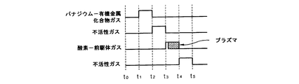
図1は、本発明の第1実施例によってバナジウム酸化物薄膜を製造する原子層蒸着方法を説明するためのタイミング図である。
(First embodiment)
FIG. 1 is a timing diagram for explaining an atomic layer deposition method for producing a vanadium oxide thin film according to a first embodiment of the present invention.
図1を参照すれば、まず、基板をチャンバにローディングする(t0〜t1)。次いで、バナジウム酸化物の前駆体であるバナジウム−有機金属化合物をチャンバに注入し、表面飽和吸着によって基板の表面にバナジウムを含有する吸着物を形成させる(t1〜t2)。ここで、表面飽和吸着とは、基板の表面に吸着物が一層に何れも吸着された後には、ガスをさらに注入しても、それ以上吸着されないということを意味する。吸着されずにチャンバに残存するバナジウム−有機金属化合物ガスをパージするために、チャンバに不活性ガス、例えば、窒素ガスを注入する(t2〜t3)。チャンバに酸素−前駆体を注入し、酸素前駆体を前記吸着物と表面飽和反応させることによって、単層のバナジウム酸化物薄膜を形成する(t3〜t4)。ここで、表面飽和反応とは、バナジウムを含む吸着物が吸着物の表面上の酸化剤と反応し、酸化剤をさらに注入しても吸着がそれ以上起きないということを意味する。次いで、チャンバに残存する反応副産物をパージするために、チャンバに不活性ガスを注入する(t4〜t5)。 Referring to FIG. 1, first, a substrate is loaded into a chamber (t 0 to t 1 ). Next, a vanadium-organometallic compound, which is a precursor of vanadium oxide, is injected into the chamber, and an adsorbate containing vanadium is formed on the surface of the substrate by surface saturated adsorption (t 1 to t 2 ). Here, the surface-saturated adsorption means that no more adsorbed substances are adsorbed even if gas is further injected after all adsorbed substances are adsorbed on the surface of the substrate. In order to purge the vanadium-organometallic compound gas remaining in the chamber without being adsorbed, an inert gas, for example, nitrogen gas is injected into the chamber (t 2 to t 3 ). A single-layer vanadium oxide thin film is formed by injecting an oxygen-precursor into the chamber and causing the oxygen precursor to surface-saturate with the adsorbate (t 3 to t 4 ). Here, the surface saturation reaction means that an adsorbate containing vanadium reacts with an oxidant on the surface of the adsorbate, and no further adsorption occurs even if an oxidant is further injected. Next, an inert gas is injected into the chamber in order to purge the reaction byproducts remaining in the chamber (t 4 to t 5 ).
バナジウム酸化物の前駆体であるバナジウム−有機金属化合物で、前記バナジウムの原子価は、+3、+4または+5のうち何れか一つでありうる。例えば、原子価が+4であるバナジウムを含むバナジウム−有機金属化合物は、テトラジエチルアミノバナジウム(V(NEt2)4)、テトラエチルメチルアミノバナジウム(V{N(EtMe)}4)またはテトラジメチルアミノバナジウム(V(NMe2)4)のうちから選択された少なくとも何れか一つでありうる。このとき、Meは、CH3であり、Etは、C2H5である。原子価が+5であるバナジウムを含むバナジウム−有機金属化合物は、トリエチルメチルアミノオキシバナジウム(VO{N(EtMe)}3)、トリジメチルアミノオキシバナジウム(VO(NMe2)3)、トリメトキシオキシバナジウム(VO(OMe)3)、トリエトキシオキシバナジウム(VO(OEt)3)、トリプロポキシバナジウム(VO(OC3H7)3)及びトリハロゲンオキシバナジウム(VOX3(X=Cl、F、Br、またはI))のうちから選択された少なくとも何れか一つでありうる。このとき、Meは、CH3であり、Etは、C2H5である。その他、バナジウム−有機金属化合物は、トリハロゲンバナジウム(VX3(X=Cl、F、Br、またはI))、テトラハロゲンバナジウム(VX4(X=Cl、F、Br、またはI))バナジウムヘキサカルボニル、バナジウム2,4−ペンタジオネート、バナジウムアセトンアセトネート及びシクロペンタジエニルバナジウムテトラカルボニルのうちから選択された少なくとも何れか一つでありうる。酸素−前駆体は、H2Oのような酸化剤を使用しうる。 In the vanadium-organometallic compound that is a precursor of vanadium oxide, the valence of the vanadium may be any one of +3, +4, and +5. For example, a vanadium-organometallic compound containing vanadium having a valence of +4 is tetradiethylaminovanadium (V (NEt 2 ) 4 ), tetraethylmethylaminovanadium (V {N (EtMe)} 4 ) or tetradimethylaminovanadium ( V (NMe 2 ) 4 ) may be at least one selected from V (NMe 2 ) 4 ). At this time, Me is CH 3 and Et is C 2 H 5 . Vanadium-organometallic compounds containing vanadium having a valence of +5 are triethylmethylaminooxyvanadium (VO {N (EtMe)} 3 ), tridimethylaminooxyvanadium (VO (NMe 2 ) 3 ), trimethoxyoxyvanadium. (VO (OMe) 3), triethoxy oxyvanadium (VO (OEt) 3), tripropoxy vanadium (VO (OC 3 H 7) 3) and tri halogen oxyvanadium (VOX 3 (X = Cl, F, Br, Or at least one selected from I)). At this time, Me is CH 3 and Et is C 2 H 5 . In addition, vanadium-organometallic compounds include trihalogen vanadium (VX 3 (X = Cl, F, Br, or I)), tetrahalogen vanadium (VX 4 (X = Cl, F, Br, or I)) vanadium hexa. It may be at least one selected from carbonyl, vanadium 2,4-pentadionate, vanadium acetone acetonate, and cyclopentadienyl vanadium tetracarbonyl. Oxygen - precursors may be used an oxidizing agent such as H 2 O.
ソース供給装置の温度は、バナジウム−有機金属化合物の蒸気圧が0.01〜10torrとなるように維持し、前記蒸気圧による注入時間によって、反応に必要なバナジウム−有機金属化合物の量が適切に調節される。バナジウム−有機金属化合物ガスは、約300℃以下でも十分に供給される。 The temperature of the source supply device is maintained so that the vapor pressure of the vanadium-organometallic compound is 0.01 to 10 torr, and the amount of vanadium-organometallic compound required for the reaction is appropriately determined according to the injection time by the vapor pressure. Adjusted. The vanadium-organometallic compound gas is sufficiently supplied even at about 300 ° C. or less.
原子層蒸着法は、表面飽和反応を利用するという点で通常のCVDと大きく異なる。原子層蒸着法で、蒸着は、原子層単位で行われ、基板の表面が粗いか、または基板に形成される構造物の縦横比が大きくても、均一な薄膜が得られる。原子層蒸着法を利用すれば、前駆体を過量に供給しても、表面飽和現象によって蒸着速度は一定に維持される。一方、PECVDの場合には、V2O5薄膜を得た後、前記V2O5薄膜を熱処理してVO2薄膜を製造する。しかし、本発明の第1実施例では、安定した組成を有するVO2薄膜を直接形成しうる。 Atomic layer deposition differs greatly from normal CVD in that it utilizes a surface saturation reaction. In the atomic layer deposition method, the deposition is performed in units of atomic layers, and a uniform thin film can be obtained even if the surface of the substrate is rough or the aspect ratio of the structure formed on the substrate is large. If the atomic layer deposition method is used, even if the precursor is supplied in an excessive amount, the deposition rate is kept constant by the surface saturation phenomenon. On the other hand, in the case of PECVD, after obtaining V 2 O 5 thin film, to produce a VO 2 thin film by heat-treating the V 2 O 5 thin film. However, in the first embodiment of the present invention, a VO 2 thin film having a stable composition can be directly formed.
(第2実施例)
図2は、本発明の第2実施例による原子層蒸着方法を説明するためのタイミング図である。第2実施例は、酸素−前駆体である酸素ガスをプラズマ状態に変換させるという点を除いては、第1実施例と同じである。
(Second embodiment)
FIG. 2 is a timing diagram for explaining an atomic layer deposition method according to a second embodiment of the present invention. The second embodiment is the same as the first embodiment except that oxygen gas, which is an oxygen-precursor, is converted into a plasma state.
図2を参照すれば、酸素−前駆体ガス、例えば、酸素ガスをプラズマ状態に変換させる(t3〜t4)。酸素ガスのプラズマ状態は、酸素前駆体の注入時間(t3〜t4)と同一かまたはそれより短い時間の間持続される。具体的に、プラズマは、前記チャンバ内に酸素前駆体を注入すると同時に形成されるか、または前記注入後に所定時間が経過した時に形成される。前記プラズマは、前記反応チャンバ内で直接形成されるか、または隣接プラズマチャンバで反応性粒子を作り、これを反応チャンバ内に注入するリモート方式を通じて形成されることもある。 Referring to FIG. 2, an oxygen-precursor gas, for example, oxygen gas, is converted into a plasma state (t 3 to t 4 ). The plasma state of the oxygen gas is maintained for a time equal to or shorter than the oxygen precursor injection time (t 3 to t 4 ). Specifically, the plasma is formed at the same time as the oxygen precursor is injected into the chamber, or is formed when a predetermined time elapses after the injection. The plasma may be formed directly in the reaction chamber or may be formed through a remote system in which reactive particles are made in an adjacent plasma chamber and injected into the reaction chamber.
本発明の第2実施例による原子層蒸着法で、蒸着は、原子層単位で起き、基板の表面が粗いか、または基板に形成された構造物の縦横比が大きくても、均一な薄膜が得られる。原子層蒸着法を利用すれば、前駆体を過量に供給しても表面飽和現象によって蒸着速度は一定に維持される。一方、PECVDの場合には、V2O5薄膜を得た後、前記V2O5薄膜を熱処理してVO2薄膜を製造する。しかし、本発明の第2実施例では、安定した組成を有するVO2薄膜を直接形成しうる。また、第2実施例で、前記第1実施例と比較して、低い反応温度でも前記VO2薄膜を形成しうる。さらに、プラズマ状態が十分に維持される場合、前記バナジウム酸化膜の結晶度は、さらに向上しうる。 In the atomic layer deposition method according to the second embodiment of the present invention, the deposition occurs in atomic layer units, and even if the surface of the substrate is rough or the aspect ratio of the structure formed on the substrate is large, a uniform thin film is formed. can get. If the atomic layer deposition method is used, the deposition rate is kept constant by the surface saturation phenomenon even if the precursor is supplied in an excessive amount. On the other hand, in the case of PECVD, after obtaining V 2 O 5 thin film, to produce a VO 2 thin film by heat-treating the V 2 O 5 thin film. However, in the second embodiment of the present invention, a VO 2 thin film having a stable composition can be directly formed. In the second embodiment, the VO 2 thin film can be formed even at a lower reaction temperature than in the first embodiment. Furthermore, when the plasma state is sufficiently maintained, the crystallinity of the vanadium oxide film can be further improved.
(実験例)
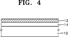
図3及び図4を参照して示したように、前記第2実施例で説明したバナジウム酸化物薄膜(以下、バナジウム酸化膜12)を備える素子を製作した。図4は、必要に応じて、図3の素子にバッファ層14をさらに形成したものである。
(Experimental example)
As shown in FIGS. 3 and 4, an element including the vanadium oxide thin film (hereinafter referred to as vanadium oxide film 12) described in the second embodiment was manufactured. FIG. 4 shows a case where a
前記バナジウム酸化膜12を製造するために、まず約12インチ径のシリコン基板10を準備する。次いで、テトラエチルメチルアミノバナジウム[V{N(EtMe}4、TEMAV]をチャンバに注入して前記シリコン基板10上にバナジウムを含有する吸着物を形成し、チャンバ内に不活性ガスを注入して残存するガスをパージした。次いで、酸素ガスをチャンバ内に注入してプラズマ状態に変換させ、単層のバナジウム酸化膜12を形成した。次いで、不活性ガスを注入して残存する反応副産物をパージ(purge)した。前述した過程を数回反復して、300nmのバナジウム酸化膜を製造した。また、バッファ層14として、TiO2膜を100nmの厚さに形成した。
In order to manufacture the
反応副産物をパージした後に、バナジウム酸化膜12をイン・サイチュ(in situ)方式によって熱処理しうる。このとき、前記熱処理は、生成されたバナジウム酸化膜12の欠陥を除去するためのものであって、バナジウム酸化物の相を変化させるためのものではない。前記熱処理は、前記チャンバ内で実施するか、または前記チャンバの雰囲気と類似した雰囲気を有する隣接チャンバで実施しうる。
After purging the reaction byproducts, the
通常、金属−絶縁体転移特性を示すバナジウム酸化膜を形成するために、サファイア単結晶を基板として使用する。それは、サファイア単結晶は、バナジウム酸化膜と格子定数が類似しており、優秀な結晶性を有するバナジウム酸化膜を成長させうるためである。しかし、サファイア基板は、コストが高く、大口径に製造し難い。これにより、本発明では、大口径、例えば、12インチのシリコン基板を使用する。8インチ以上の直径を有する大口径の製造が容易なガラスまたは水晶基板も使われる。 Usually, a sapphire single crystal is used as a substrate to form a vanadium oxide film exhibiting metal-insulator transition characteristics. This is because the sapphire single crystal has a lattice constant similar to that of the vanadium oxide film and can grow a vanadium oxide film having excellent crystallinity. However, sapphire substrates are expensive and difficult to manufacture in large diameters. Accordingly, in the present invention, a silicon substrate having a large diameter, for example, 12 inches is used. A glass or quartz substrate that has a diameter of 8 inches or more and is easy to manufacture can be used.
バッファ層14は、バナジウム酸化膜の結晶性を改善するために、バナジウム酸化膜の格子定数と類似した値を有する結晶性薄膜を使用しうる。例えば、バッファ層14は、酸化アルミニウム膜、高誘電膜、結晶性金属膜及びシリコン酸化膜で構成される群から選択される少なくとも何れか一つでありうる。このとき、酸化アルミニウム膜は、結晶性がある程度維持される程度ならば十分であり、シリコン酸化膜は、可能なかぎり薄く形成される。特に、結晶性に優れた高誘電膜、例えば、TiO2膜、ZrO2膜、Ta2O5膜及びHfO2膜またはこれらの混合膜及び/または結晶性金属膜を含む多層膜をバッファ層14として形成しうる。バッファ層14上のバナジウム酸化膜12に十分なエネルギーを加えるように、プラズマ状態を十分に維持すれば、バナジウム酸化膜12の結晶性をさらに向上させうる。
The
図5は、温度による前記バナジウム酸化膜の蒸着速度を示すグラフである。図5を参照すれば、100℃〜170℃の温度範囲(A状態)では、バナジウム酸化膜の蒸着速度は、温度に依存せず、一定の蒸着速度を示している。これは、バナジウム酸化膜が表面飽和反応によって形成されることを意味する。 FIG. 5 is a graph showing the deposition rate of the vanadium oxide film according to temperature. Referring to FIG. 5, in the temperature range (A state) of 100 ° C. to 170 ° C., the deposition rate of the vanadium oxide film does not depend on the temperature and shows a constant deposition rate. This means that the vanadium oxide film is formed by a surface saturation reaction.
一方、約170℃以上の温度範囲(B状態)では、温度によって蒸着速度が向上する。温度による蒸着速度の向上は、バナジウム酸化膜がCVD方式で蒸着されることを意味する。具体的に、約170℃以上では、バナジウム酸化物の前駆体が気相に分解され、前駆体間に反応が進められて、表面飽和反応でないガス状態の反応によってCVDが起きる。したがって、蒸着速度は、温度が上昇するほど上昇する。CVD方式でバナジウム酸化膜が蒸着されれば、形成される薄膜の厚さが不均一になり、前記薄膜の組成が不安定になる。 On the other hand, in the temperature range (B state) of about 170 ° C. or higher, the deposition rate is improved depending on the temperature. Improvement of the deposition rate with temperature means that the vanadium oxide film is deposited by the CVD method. Specifically, at about 170 ° C. or higher, the vanadium oxide precursor is decomposed into a gas phase, the reaction proceeds between the precursors, and CVD occurs due to a gas-state reaction that is not a surface saturation reaction. Therefore, the deposition rate increases as the temperature increases. If the vanadium oxide film is deposited by the CVD method, the thickness of the formed thin film becomes non-uniform, and the composition of the thin film becomes unstable.
一方、原子層蒸着方式の代りに、CVDのおきる温度は、バナジウム酸化物の前駆体によって変わりうる。例えば、トリプロトキシドオキシバナジウム(VO(OC3H7)3)を前駆体として使用すれば、前記温度は、約200℃である。トリクロライドオキシバナジウム(VOCl3)を前駆体として使用すれば、前記温度は、約300℃である。そして、トリハロゲン化バナジウムまたはテトラハロゲン化バナジウムが前駆体として使われる場合、さらに高い温度、例えば、350〜500℃を要求するが、これにより、500℃まで蒸着温度を上昇させることが可能である。したがって、バナジウム酸化物の前駆体によって、原子層蒸着方式で形成されるバナジウム酸化膜12の形成温度は、100℃〜500℃となりうる。
On the other hand, instead of atomic layer deposition, the temperature at which CVD occurs can vary depending on the vanadium oxide precursor. For example, if triprotooxide oxyvanadium (VO (OC 3 H 7 ) 3 ) is used as a precursor, the temperature is about 200 ° C. If trichloride oxyvanadium (VOCl 3 ) is used as a precursor, the temperature is about 300 ° C. When vanadium trihalide or vanadium tetrahalide is used as a precursor, a higher temperature, for example, 350 to 500 ° C. is required, which can increase the deposition temperature to 500 ° C. . Therefore, the formation temperature of the
図6は、150℃で製作したバナジウム酸化膜の組成をオージェ電子顕微鏡(AES)を利用して分析して示すグラフである。このとき、エッチング時間は、AES分析のためのバナジウム酸化膜をエッチングする時間である。前記エッチング時間が約900秒を経過すれば、バナジウム酸化膜とSi基板との間にSi基板の境界部分(VO2/Si)が現れる。図6に示したように、バナジウムと酸素との組成比は、約1:2であり、原子価が+4であるバナジウムが、原子価が−2である酸素と結合してVO2を形成するということが分かる。すなわち、VO2薄膜は、化学的に安定している。 FIG. 6 is a graph showing the composition of a vanadium oxide film fabricated at 150 ° C. analyzed using an Auger electron microscope (AES). At this time, the etching time is a time for etching the vanadium oxide film for AES analysis. If the etching time passes about 900 seconds, a boundary portion (VO 2 / Si) of the Si substrate appears between the vanadium oxide film and the Si substrate. As shown in FIG. 6, the composition ratio of vanadium and oxygen is about 1: 2, and vanadium having a valence of +4 combines with oxygen having a valence of −2 to form VO 2 . I understand that. That is, the VO 2 thin film is chemically stable.
図7は、図5のバナジウム酸化膜の温度による抵抗変化を示すグラフである。図7に示したように、プラズマ原子層蒸着法で蒸着されたバナジウム酸化膜は、所定の熱処理過程を経た後、約65℃(335K)の近くで急激な金属−絶縁体転移を示す。すなわち、バナジウム酸化膜の抵抗値は、約50,000Ωから約10Ωに急減する。本発明によるバナジウム酸化膜は、約50,000Ωの抵抗値の変化、すなわち、電気伝導度の上昇をもたらす。 FIG. 7 is a graph showing the resistance change with temperature of the vanadium oxide film of FIG. As shown in FIG. 7, the vanadium oxide film deposited by the plasma atomic layer deposition method exhibits a rapid metal-insulator transition near about 65 ° C. (335 K) after a predetermined heat treatment process. That is, the resistance value of the vanadium oxide film rapidly decreases from about 50,000Ω to about 10Ω. The vanadium oxide film according to the present invention causes a change in resistance value of about 50,000 Ω, that is, an increase in electrical conductivity.
本発明は、例示的な実施例を挙げて詳細に説明したが、本発明は、前記実施例に限定されず、本発明の技術的思想の範囲内で、当業者によって色々な変形が可能である。 Although the present invention has been described in detail with reference to exemplary embodiments, the present invention is not limited to the above-described embodiments, and various modifications can be made by those skilled in the art within the scope of the technical idea of the present invention. is there.
Claims (14)
表面飽和吸着によって均一に前記基板上にバナジウムを含む吸着物を形成させるために、バナジウム−有機金属化合物ガスを前記チャンバに注入する工程と、
前記チャンバ内に不活性ガスを注入して、未吸着の前記バナジウム−有機金属化合物ガスをパージする工程と、
前記チャンバに酸素前駆体を注入して、前記酸素前駆体と前記吸着物とを表面飽和反応させてバナジウム酸化物薄膜を形成する工程と、を含み、
前記バナジウム−有機金属化合物がテトラエチルメチルアミノバナジウム(V{N(C2H5CH3)}4:TEMAV)であり、
前記チャンバに酸素前駆体を注入してプラズマ状態に変化させ所定時間持続させるバナジウム酸化物薄膜の製造方法。Loading a substrate into the chamber;
Injecting a vanadium-organometallic compound gas into the chamber to uniformly form an adsorbate containing vanadium on the substrate by surface saturated adsorption;
Injecting an inert gas into the chamber to purge the unadsorbed vanadium-organometallic compound gas;
Injecting an oxygen precursor into the chamber to cause a surface saturation reaction between the oxygen precursor and the adsorbate to form a vanadium oxide thin film,
The vanadium-organometallic compound is tetraethylmethylamino vanadium (V {N (C 2 H 5 CH 3 )} 4 : TEMAV);
A method for producing a vanadium oxide thin film, in which an oxygen precursor is injected into the chamber to be changed into a plasma state and maintained for a predetermined time.
前記基板上に前記バナジウム酸化物薄膜の格子定数と類似した格子定数を有するバッファ層を形成する工程をさらに含むことを特徴とする請求項1に記載のバナジウム酸化物薄膜の製造方法。Before the step of injecting the vanadium-organometallic compound gas,
Method for producing a vanadium oxide thin film according to claim 1, characterized by further comprising the step of forming a buffer layer with similar lattice constant as that of the vanadium oxide thin film on the substrate.
前記バナジウム酸化物薄膜をイン・サイチュ方式によって熱処理する工程をさらに含むことを特徴とする請求項1に記載のバナジウム酸化物薄膜の製造方法。After the step of purging reaction by-products (the unadsorbed vanadium-organometallic compound gas),
The method for producing a vanadium oxide thin film according to claim 1, further comprising a step of heat-treating the vanadium oxide thin film by an in situ method.
表面飽和吸着によって前記Si基板の表面上にバナジウムを含む吸着物を形成させるために、テトラエチルメチルアミノバナジウム(V{N(C2H5CH3)}4:TEMAV)ガスを前記チャンバに注入する工程と、
未吸着の前記TEMAVガスをパージするために、前記チャンバ内に不活性ガスを注入する工程と、
前記チャンバにH2Oを注入し、前記H2Oが前記吸着物と表面飽和反応してバナジウム酸化物薄膜を形成させる工程と、
前記チャンバに残存する反応副産物をパージするために、前記チャンバ内に不活性ガスを注入する工程と、を含み、
前記チャンバにH2Oを注入してプラズマ状態に変化させ所定時間持続させ、
前記表面飽和吸着及び表面飽和反応を所定回数反復するバナジウム酸化物薄膜の製造方法。Loading a Si substrate into the chamber;
Tetraethylmethylamino vanadium (V {N (C 2 H 5 CH 3 )} 4 : TEMAV) gas is injected into the chamber to form an adsorbate containing vanadium on the surface of the Si substrate by surface saturated adsorption. Process,
Injecting an inert gas into the chamber to purge the unadsorbed TEMAV gas;
Injecting H 2 O into the chamber and causing the H 2 O to surface-saturate with the adsorbate to form a vanadium oxide thin film;
Injecting an inert gas into the chamber to purge reaction by-products remaining in the chamber;
H 2 O is injected into the chamber to change to a plasma state and continue for a predetermined time,
A method for producing a vanadium oxide thin film in which the surface saturated adsorption and the surface saturated reaction are repeated a predetermined number of times.
テトラエチルメチルアミノバナジウム(V{N(C2H5CH3)}4:TEMAV)ガスを前記チャンバに注入し、表面飽和反応によって前記Si基板の表面上にバナジウムを含む吸着物を形成させる工程と、
未吸着のTEMAVガスをパージするために、前記チャンバの内部に不活性ガスを注入する工程と、
酸素前駆体をプラズマ状態に変化させ、前記チャンバの内部に前記酸素前駆体をプラズマ状態で所定時間注入して、前記プラズマ状態の酸素前駆体が前記吸着物と表面飽和反応することによって、バナジウム酸化物薄膜を形成させる工程と、
前記チャンバに残存する反応副産物をパージするために、前記チャンバに非活性ガスを注入する工程と、を含み、
前記表面飽和吸着及び表面飽和反応を所定回数反復するバナジウム酸化物薄膜の製造方法。Loading a Si substrate into the chamber;
Injecting tetraethylmethylamino vanadium (V {N (C 2 H 5 CH 3 )} 4 : TEMAV) gas into the chamber to form an adsorbate containing vanadium on the surface of the Si substrate by a surface saturation reaction; ,
Injecting an inert gas into the chamber to purge unadsorbed TEMAV gas;
Vanadium oxidation is performed by changing the oxygen precursor to a plasma state, injecting the oxygen precursor into the chamber in a plasma state for a predetermined time, and causing the plasma state oxygen precursor to surface-saturate with the adsorbate. Forming a physical thin film;
Injecting an inert gas into the chamber to purge reaction byproducts remaining in the chamber;
A method for producing a vanadium oxide thin film in which the surface saturated adsorption and the surface saturated reaction are repeated a predetermined number of times.
Applications Claiming Priority (5)
| Application Number | Priority Date | Filing Date | Title |
|---|---|---|---|
| KR10-2005-0077843 | 2005-08-24 | ||
| KR20050077843 | 2005-08-24 | ||
| KR1020050117265A KR100734854B1 (en) | 2005-08-24 | 2005-12-03 | Method of manufacturing thin film of vanadiun di-oxide |
| KR10-2005-0117265 | 2005-12-03 | ||
| PCT/KR2006/003307 WO2007024094A1 (en) | 2005-08-24 | 2006-08-23 | Method of manufacturing vanadium oxide thin film |
Publications (2)
| Publication Number | Publication Date |
|---|---|
| JP2009506207A JP2009506207A (en) | 2009-02-12 |
| JP5184357B2 true JP5184357B2 (en) | 2013-04-17 |
Family
ID=37771802
Family Applications (1)
| Application Number | Title | Priority Date | Filing Date |
|---|---|---|---|
| JP2008527846A Expired - Fee Related JP5184357B2 (en) | 2005-08-24 | 2006-08-23 | Method for producing vanadium oxide thin film |
Country Status (3)
| Country | Link |
|---|---|
| US (1) | US20090011145A1 (en) |
| JP (1) | JP5184357B2 (en) |
| WO (1) | WO2007024094A1 (en) |
Families Citing this family (293)
| Publication number | Priority date | Publication date | Assignee | Title |
|---|---|---|---|---|
| DE102007042721A1 (en) * | 2007-09-07 | 2009-03-12 | Robert Bosch Gmbh | Hand tool with a vibration-dampened by a compensating means handle |
| US10378106B2 (en) | 2008-11-14 | 2019-08-13 | Asm Ip Holding B.V. | Method of forming insulation film by modified PEALD |
| US9394608B2 (en) | 2009-04-06 | 2016-07-19 | Asm America, Inc. | Semiconductor processing reactor and components thereof |
| US8802201B2 (en) | 2009-08-14 | 2014-08-12 | Asm America, Inc. | Systems and methods for thin-film deposition of metal oxides using excited nitrogen-oxygen species |
| US9184382B2 (en) | 2010-10-28 | 2015-11-10 | Hewlett-Packard Development Company, L.P. | Memristive devices with layered junctions and methods for fabricating the same |
| CN102603203B (en) * | 2011-01-25 | 2014-06-18 | 中国科学院上海硅酸盐研究所 | Preparation method of vanadium dioxide film |
| KR101770314B1 (en) | 2011-03-04 | 2017-08-23 | 삼성전자주식회사 | Methods of forming an dielectric layer and methods of manufacturing a semiconductor device using the same |
| US9312155B2 (en) | 2011-06-06 | 2016-04-12 | Asm Japan K.K. | High-throughput semiconductor-processing apparatus equipped with multiple dual-chamber modules |
| US10364496B2 (en) | 2011-06-27 | 2019-07-30 | Asm Ip Holding B.V. | Dual section module having shared and unshared mass flow controllers |
| US10854498B2 (en) | 2011-07-15 | 2020-12-01 | Asm Ip Holding B.V. | Wafer-supporting device and method for producing same |
| US20130023129A1 (en) | 2011-07-20 | 2013-01-24 | Asm America, Inc. | Pressure transmitter for a semiconductor processing environment |
| US9017481B1 (en) | 2011-10-28 | 2015-04-28 | Asm America, Inc. | Process feed management for semiconductor substrate processing |
| WO2013184556A1 (en) | 2012-06-05 | 2013-12-12 | President And Fellows Of Harvard College | Ultra-thin optical coatings and devices and methods of using ultra-thin optical coatings |
| US9659799B2 (en) | 2012-08-28 | 2017-05-23 | Asm Ip Holding B.V. | Systems and methods for dynamic semiconductor process scheduling |
| US10714315B2 (en) | 2012-10-12 | 2020-07-14 | Asm Ip Holdings B.V. | Semiconductor reaction chamber showerhead |
| US9589770B2 (en) | 2013-03-08 | 2017-03-07 | Asm Ip Holding B.V. | Method and systems for in-situ formation of intermediate reactive species |
| US9484191B2 (en) | 2013-03-08 | 2016-11-01 | Asm Ip Holding B.V. | Pulsed remote plasma method and system |
| US9240412B2 (en) | 2013-09-27 | 2016-01-19 | Asm Ip Holding B.V. | Semiconductor structure and device and methods of forming same using selective epitaxial process |
| US10683571B2 (en) | 2014-02-25 | 2020-06-16 | Asm Ip Holding B.V. | Gas supply manifold and method of supplying gases to chamber using same |
| US10167557B2 (en) | 2014-03-18 | 2019-01-01 | Asm Ip Holding B.V. | Gas distribution system, reactor including the system, and methods of using the same |
| US11015245B2 (en) | 2014-03-19 | 2021-05-25 | Asm Ip Holding B.V. | Gas-phase reactor and system having exhaust plenum and components thereof |
| US10858737B2 (en) | 2014-07-28 | 2020-12-08 | Asm Ip Holding B.V. | Showerhead assembly and components thereof |
| US9890456B2 (en) | 2014-08-21 | 2018-02-13 | Asm Ip Holding B.V. | Method and system for in situ formation of gas-phase compounds |
| US9657845B2 (en) | 2014-10-07 | 2017-05-23 | Asm Ip Holding B.V. | Variable conductance gas distribution apparatus and method |
| US10941490B2 (en) | 2014-10-07 | 2021-03-09 | Asm Ip Holding B.V. | Multiple temperature range susceptor, assembly, reactor and system including the susceptor, and methods of using the same |
| US20160168699A1 (en) * | 2014-12-12 | 2016-06-16 | Asm Ip Holding B.V. | Method for depositing metal-containing film using particle-reduction step |
| KR102263121B1 (en) | 2014-12-22 | 2021-06-09 | 에이에스엠 아이피 홀딩 비.브이. | Semiconductor device and manufacuring method thereof |
| US10529542B2 (en) | 2015-03-11 | 2020-01-07 | Asm Ip Holdings B.V. | Cross-flow reactor and method |
| US10276355B2 (en) | 2015-03-12 | 2019-04-30 | Asm Ip Holding B.V. | Multi-zone reactor, system including the reactor, and method of using the same |
| US10458018B2 (en) | 2015-06-26 | 2019-10-29 | Asm Ip Holding B.V. | Structures including metal carbide material, devices including the structures, and methods of forming same |
| US10600673B2 (en) | 2015-07-07 | 2020-03-24 | Asm Ip Holding B.V. | Magnetic susceptor to baseplate seal |
| US9960072B2 (en) | 2015-09-29 | 2018-05-01 | Asm Ip Holding B.V. | Variable adjustment for precise matching of multiple chamber cavity housings |
| US10211308B2 (en) | 2015-10-21 | 2019-02-19 | Asm Ip Holding B.V. | NbMC layers |
| US10322384B2 (en) | 2015-11-09 | 2019-06-18 | Asm Ip Holding B.V. | Counter flow mixer for process chamber |
| US11139308B2 (en) | 2015-12-29 | 2021-10-05 | Asm Ip Holding B.V. | Atomic layer deposition of III-V compounds to form V-NAND devices |
| US10529554B2 (en) | 2016-02-19 | 2020-01-07 | Asm Ip Holding B.V. | Method for forming silicon nitride film selectively on sidewalls or flat surfaces of trenches |
| US10468251B2 (en) | 2016-02-19 | 2019-11-05 | Asm Ip Holding B.V. | Method for forming spacers using silicon nitride film for spacer-defined multiple patterning |
| US10501866B2 (en) | 2016-03-09 | 2019-12-10 | Asm Ip Holding B.V. | Gas distribution apparatus for improved film uniformity in an epitaxial system |
| US10343920B2 (en) | 2016-03-18 | 2019-07-09 | Asm Ip Holding B.V. | Aligned carbon nanotubes |
| US9892913B2 (en) | 2016-03-24 | 2018-02-13 | Asm Ip Holding B.V. | Radial and thickness control via biased multi-port injection settings |
| US10865475B2 (en) | 2016-04-21 | 2020-12-15 | Asm Ip Holding B.V. | Deposition of metal borides and silicides |
| WO2017184701A1 (en) | 2016-04-21 | 2017-10-26 | Applied Materials, Inc. | Doped and undoped vanadium oxides for low-k spacer applications |
| US10190213B2 (en) | 2016-04-21 | 2019-01-29 | Asm Ip Holding B.V. | Deposition of metal borides |
| US10032628B2 (en) | 2016-05-02 | 2018-07-24 | Asm Ip Holding B.V. | Source/drain performance through conformal solid state doping |
| US10367080B2 (en) | 2016-05-02 | 2019-07-30 | Asm Ip Holding B.V. | Method of forming a germanium oxynitride film |
| KR102592471B1 (en) | 2016-05-17 | 2023-10-20 | 에이에스엠 아이피 홀딩 비.브이. | Method of forming metal interconnection and method of fabricating semiconductor device using the same |
| US11453943B2 (en) | 2016-05-25 | 2022-09-27 | Asm Ip Holding B.V. | Method for forming carbon-containing silicon/metal oxide or nitride film by ALD using silicon precursor and hydrocarbon precursor |
| US10388509B2 (en) | 2016-06-28 | 2019-08-20 | Asm Ip Holding B.V. | Formation of epitaxial layers via dislocation filtering |
| US9859151B1 (en) | 2016-07-08 | 2018-01-02 | Asm Ip Holding B.V. | Selective film deposition method to form air gaps |
| US10612137B2 (en) | 2016-07-08 | 2020-04-07 | Asm Ip Holdings B.V. | Organic reactants for atomic layer deposition |
| US10714385B2 (en) | 2016-07-19 | 2020-07-14 | Asm Ip Holding B.V. | Selective deposition of tungsten |
| KR102354490B1 (en) | 2016-07-27 | 2022-01-21 | 에이에스엠 아이피 홀딩 비.브이. | Method of processing a substrate |
| US10395919B2 (en) | 2016-07-28 | 2019-08-27 | Asm Ip Holding B.V. | Method and apparatus for filling a gap |
| US9887082B1 (en) | 2016-07-28 | 2018-02-06 | Asm Ip Holding B.V. | Method and apparatus for filling a gap |
| KR102532607B1 (en) | 2016-07-28 | 2023-05-15 | 에이에스엠 아이피 홀딩 비.브이. | Substrate processing apparatus and method of operating the same |
| US9812320B1 (en) | 2016-07-28 | 2017-11-07 | Asm Ip Holding B.V. | Method and apparatus for filling a gap |
| CN107779820B (en) * | 2016-08-26 | 2019-11-19 | 中国科学院上海硅酸盐研究所 | A kind of vanadium dioxide film and its low temperature deposition method |
| US10410943B2 (en) | 2016-10-13 | 2019-09-10 | Asm Ip Holding B.V. | Method for passivating a surface of a semiconductor and related systems |
| US10643826B2 (en) | 2016-10-26 | 2020-05-05 | Asm Ip Holdings B.V. | Methods for thermally calibrating reaction chambers |
| US11532757B2 (en) | 2016-10-27 | 2022-12-20 | Asm Ip Holding B.V. | Deposition of charge trapping layers |
| US10643904B2 (en) | 2016-11-01 | 2020-05-05 | Asm Ip Holdings B.V. | Methods for forming a semiconductor device and related semiconductor device structures |
| US10435790B2 (en) | 2016-11-01 | 2019-10-08 | Asm Ip Holding B.V. | Method of subatmospheric plasma-enhanced ALD using capacitively coupled electrodes with narrow gap |
| US10229833B2 (en) | 2016-11-01 | 2019-03-12 | Asm Ip Holding B.V. | Methods for forming a transition metal nitride film on a substrate by atomic layer deposition and related semiconductor device structures |
| US10714350B2 (en) | 2016-11-01 | 2020-07-14 | ASM IP Holdings, B.V. | Methods for forming a transition metal niobium nitride film on a substrate by atomic layer deposition and related semiconductor device structures |
| US10134757B2 (en) | 2016-11-07 | 2018-11-20 | Asm Ip Holding B.V. | Method of processing a substrate and a device manufactured by using the method |
| KR102546317B1 (en) | 2016-11-15 | 2023-06-21 | 에이에스엠 아이피 홀딩 비.브이. | Gas supply unit and substrate processing apparatus including the same |
| US10340135B2 (en) | 2016-11-28 | 2019-07-02 | Asm Ip Holding B.V. | Method of topologically restricted plasma-enhanced cyclic deposition of silicon or metal nitride |
| KR20180068582A (en) | 2016-12-14 | 2018-06-22 | 에이에스엠 아이피 홀딩 비.브이. | Substrate processing apparatus |
| US11447861B2 (en) | 2016-12-15 | 2022-09-20 | Asm Ip Holding B.V. | Sequential infiltration synthesis apparatus and a method of forming a patterned structure |
| US11581186B2 (en) | 2016-12-15 | 2023-02-14 | Asm Ip Holding B.V. | Sequential infiltration synthesis apparatus |
| KR20180070971A (en) | 2016-12-19 | 2018-06-27 | 에이에스엠 아이피 홀딩 비.브이. | Substrate processing apparatus |
| US10269558B2 (en) | 2016-12-22 | 2019-04-23 | Asm Ip Holding B.V. | Method of forming a structure on a substrate |
| US10867788B2 (en) | 2016-12-28 | 2020-12-15 | Asm Ip Holding B.V. | Method of forming a structure on a substrate |
| US10655221B2 (en) | 2017-02-09 | 2020-05-19 | Asm Ip Holding B.V. | Method for depositing oxide film by thermal ALD and PEALD |
| US10468261B2 (en) | 2017-02-15 | 2019-11-05 | Asm Ip Holding B.V. | Methods for forming a metallic film on a substrate by cyclical deposition and related semiconductor device structures |
| US10283353B2 (en) | 2017-03-29 | 2019-05-07 | Asm Ip Holding B.V. | Method of reforming insulating film deposited on substrate with recess pattern |
| US10529563B2 (en) | 2017-03-29 | 2020-01-07 | Asm Ip Holdings B.V. | Method for forming doped metal oxide films on a substrate by cyclical deposition and related semiconductor device structures |
| KR102457289B1 (en) | 2017-04-25 | 2022-10-21 | 에이에스엠 아이피 홀딩 비.브이. | Method for depositing a thin film and manufacturing a semiconductor device |
| US10770286B2 (en) | 2017-05-08 | 2020-09-08 | Asm Ip Holdings B.V. | Methods for selectively forming a silicon nitride film on a substrate and related semiconductor device structures |
| US10892156B2 (en) | 2017-05-08 | 2021-01-12 | Asm Ip Holding B.V. | Methods for forming a silicon nitride film on a substrate and related semiconductor device structures |
| US10446393B2 (en) | 2017-05-08 | 2019-10-15 | Asm Ip Holding B.V. | Methods for forming silicon-containing epitaxial layers and related semiconductor device structures |
| US10504742B2 (en) | 2017-05-31 | 2019-12-10 | Asm Ip Holding B.V. | Method of atomic layer etching using hydrogen plasma |
| US10886123B2 (en) | 2017-06-02 | 2021-01-05 | Asm Ip Holding B.V. | Methods for forming low temperature semiconductor layers and related semiconductor device structures |
| US11306395B2 (en) | 2017-06-28 | 2022-04-19 | Asm Ip Holding B.V. | Methods for depositing a transition metal nitride film on a substrate by atomic layer deposition and related deposition apparatus |
| US10685834B2 (en) | 2017-07-05 | 2020-06-16 | Asm Ip Holdings B.V. | Methods for forming a silicon germanium tin layer and related semiconductor device structures |
| KR20190009245A (en) | 2017-07-18 | 2019-01-28 | 에이에스엠 아이피 홀딩 비.브이. | Methods for forming a semiconductor device structure and related semiconductor device structures |
| US10541333B2 (en) | 2017-07-19 | 2020-01-21 | Asm Ip Holding B.V. | Method for depositing a group IV semiconductor and related semiconductor device structures |
| US11018002B2 (en) | 2017-07-19 | 2021-05-25 | Asm Ip Holding B.V. | Method for selectively depositing a Group IV semiconductor and related semiconductor device structures |
| US11374112B2 (en) | 2017-07-19 | 2022-06-28 | Asm Ip Holding B.V. | Method for depositing a group IV semiconductor and related semiconductor device structures |
| US10312055B2 (en) | 2017-07-26 | 2019-06-04 | Asm Ip Holding B.V. | Method of depositing film by PEALD using negative bias |
| US10590535B2 (en) | 2017-07-26 | 2020-03-17 | Asm Ip Holdings B.V. | Chemical treatment, deposition and/or infiltration apparatus and method for using the same |
| US10605530B2 (en) | 2017-07-26 | 2020-03-31 | Asm Ip Holding B.V. | Assembly of a liner and a flange for a vertical furnace as well as the liner and the vertical furnace |
| US10770336B2 (en) | 2017-08-08 | 2020-09-08 | Asm Ip Holding B.V. | Substrate lift mechanism and reactor including same |
| US10692741B2 (en) | 2017-08-08 | 2020-06-23 | Asm Ip Holdings B.V. | Radiation shield |
| US11769682B2 (en) | 2017-08-09 | 2023-09-26 | Asm Ip Holding B.V. | Storage apparatus for storing cassettes for substrates and processing apparatus equipped therewith |
| US10249524B2 (en) | 2017-08-09 | 2019-04-02 | Asm Ip Holding B.V. | Cassette holder assembly for a substrate cassette and holding member for use in such assembly |
| US11139191B2 (en) | 2017-08-09 | 2021-10-05 | Asm Ip Holding B.V. | Storage apparatus for storing cassettes for substrates and processing apparatus equipped therewith |
| USD900036S1 (en) | 2017-08-24 | 2020-10-27 | Asm Ip Holding B.V. | Heater electrical connector and adapter |
| US11830730B2 (en) | 2017-08-29 | 2023-11-28 | Asm Ip Holding B.V. | Layer forming method and apparatus |
| KR102491945B1 (en) | 2017-08-30 | 2023-01-26 | 에이에스엠 아이피 홀딩 비.브이. | Substrate processing apparatus |
| US11056344B2 (en) | 2017-08-30 | 2021-07-06 | Asm Ip Holding B.V. | Layer forming method |
| US11295980B2 (en) | 2017-08-30 | 2022-04-05 | Asm Ip Holding B.V. | Methods for depositing a molybdenum metal film over a dielectric surface of a substrate by a cyclical deposition process and related semiconductor device structures |
| US10607895B2 (en) | 2017-09-18 | 2020-03-31 | Asm Ip Holdings B.V. | Method for forming a semiconductor device structure comprising a gate fill metal |
| KR102630301B1 (en) | 2017-09-21 | 2024-01-29 | 에이에스엠 아이피 홀딩 비.브이. | Method of sequential infiltration synthesis treatment of infiltrateable material and structures and devices formed using same |
| US10844484B2 (en) | 2017-09-22 | 2020-11-24 | Asm Ip Holding B.V. | Apparatus for dispensing a vapor phase reactant to a reaction chamber and related methods |
| US10658205B2 (en) | 2017-09-28 | 2020-05-19 | Asm Ip Holdings B.V. | Chemical dispensing apparatus and methods for dispensing a chemical to a reaction chamber |
| US10403504B2 (en) | 2017-10-05 | 2019-09-03 | Asm Ip Holding B.V. | Method for selectively depositing a metallic film on a substrate |
| US10319588B2 (en) | 2017-10-10 | 2019-06-11 | Asm Ip Holding B.V. | Method for depositing a metal chalcogenide on a substrate by cyclical deposition |
| US10923344B2 (en) | 2017-10-30 | 2021-02-16 | Asm Ip Holding B.V. | Methods for forming a semiconductor structure and related semiconductor structures |
| US10910262B2 (en) | 2017-11-16 | 2021-02-02 | Asm Ip Holding B.V. | Method of selectively depositing a capping layer structure on a semiconductor device structure |
| KR102443047B1 (en) | 2017-11-16 | 2022-09-14 | 에이에스엠 아이피 홀딩 비.브이. | Method of processing a substrate and a device manufactured by the same |
| US11022879B2 (en) | 2017-11-24 | 2021-06-01 | Asm Ip Holding B.V. | Method of forming an enhanced unexposed photoresist layer |
| KR102597978B1 (en) | 2017-11-27 | 2023-11-06 | 에이에스엠 아이피 홀딩 비.브이. | Storage device for storing wafer cassettes for use with batch furnaces |
| US11639811B2 (en) | 2017-11-27 | 2023-05-02 | Asm Ip Holding B.V. | Apparatus including a clean mini environment |
| US10290508B1 (en) | 2017-12-05 | 2019-05-14 | Asm Ip Holding B.V. | Method for forming vertical spacers for spacer-defined patterning |
| US10872771B2 (en) | 2018-01-16 | 2020-12-22 | Asm Ip Holding B. V. | Method for depositing a material film on a substrate within a reaction chamber by a cyclical deposition process and related device structures |
| US10781517B1 (en) * | 2018-01-19 | 2020-09-22 | United States Of America As Represented By The Administrator Of Nasa | Modification of radiator pigments using atomic layer deposition (ALD) of thermal protective film material |
| TWI799494B (en) | 2018-01-19 | 2023-04-21 | 荷蘭商Asm 智慧財產控股公司 | Deposition method |
| WO2019142055A2 (en) | 2018-01-19 | 2019-07-25 | Asm Ip Holding B.V. | Method for depositing a gap-fill layer by plasma-assisted deposition |
| USD903477S1 (en) | 2018-01-24 | 2020-12-01 | Asm Ip Holdings B.V. | Metal clamp |
| US11018047B2 (en) | 2018-01-25 | 2021-05-25 | Asm Ip Holding B.V. | Hybrid lift pin |
| USD880437S1 (en) | 2018-02-01 | 2020-04-07 | Asm Ip Holding B.V. | Gas supply plate for semiconductor manufacturing apparatus |
| US10535516B2 (en) | 2018-02-01 | 2020-01-14 | Asm Ip Holdings B.V. | Method for depositing a semiconductor structure on a surface of a substrate and related semiconductor structures |
| US11081345B2 (en) | 2018-02-06 | 2021-08-03 | Asm Ip Holding B.V. | Method of post-deposition treatment for silicon oxide film |
| CN111699278B (en) | 2018-02-14 | 2023-05-16 | Asm Ip私人控股有限公司 | Method for depositing ruthenium-containing films on substrates by cyclical deposition processes |
| US10896820B2 (en) | 2018-02-14 | 2021-01-19 | Asm Ip Holding B.V. | Method for depositing a ruthenium-containing film on a substrate by a cyclical deposition process |
| US10731249B2 (en) | 2018-02-15 | 2020-08-04 | Asm Ip Holding B.V. | Method of forming a transition metal containing film on a substrate by a cyclical deposition process, a method for supplying a transition metal halide compound to a reaction chamber, and related vapor deposition apparatus |
| US10658181B2 (en) | 2018-02-20 | 2020-05-19 | Asm Ip Holding B.V. | Method of spacer-defined direct patterning in semiconductor fabrication |
| KR102636427B1 (en) | 2018-02-20 | 2024-02-13 | 에이에스엠 아이피 홀딩 비.브이. | Substrate processing method and apparatus |
| US10975470B2 (en) | 2018-02-23 | 2021-04-13 | Asm Ip Holding B.V. | Apparatus for detecting or monitoring for a chemical precursor in a high temperature environment |
| US11473195B2 (en) | 2018-03-01 | 2022-10-18 | Asm Ip Holding B.V. | Semiconductor processing apparatus and a method for processing a substrate |
| US11629406B2 (en) | 2018-03-09 | 2023-04-18 | Asm Ip Holding B.V. | Semiconductor processing apparatus comprising one or more pyrometers for measuring a temperature of a substrate during transfer of the substrate |
| US11114283B2 (en) | 2018-03-16 | 2021-09-07 | Asm Ip Holding B.V. | Reactor, system including the reactor, and methods of manufacturing and using same |
| KR102646467B1 (en) | 2018-03-27 | 2024-03-11 | 에이에스엠 아이피 홀딩 비.브이. | Method of forming an electrode on a substrate and a semiconductor device structure including an electrode |
| US11088002B2 (en) | 2018-03-29 | 2021-08-10 | Asm Ip Holding B.V. | Substrate rack and a substrate processing system and method |
| US10510536B2 (en) | 2018-03-29 | 2019-12-17 | Asm Ip Holding B.V. | Method of depositing a co-doped polysilicon film on a surface of a substrate within a reaction chamber |
| US11230766B2 (en) | 2018-03-29 | 2022-01-25 | Asm Ip Holding B.V. | Substrate processing apparatus and method |
| KR102501472B1 (en) | 2018-03-30 | 2023-02-20 | 에이에스엠 아이피 홀딩 비.브이. | Substrate processing method |
| TW202344708A (en) | 2018-05-08 | 2023-11-16 | 荷蘭商Asm Ip私人控股有限公司 | Methods for depositing an oxide film on a substrate by a cyclical deposition process and related device structures |
| TWI816783B (en) | 2018-05-11 | 2023-10-01 | 荷蘭商Asm 智慧財產控股公司 | Methods for forming a doped metal carbide film on a substrate and related semiconductor device structures |
| KR102596988B1 (en) | 2018-05-28 | 2023-10-31 | 에이에스엠 아이피 홀딩 비.브이. | Method of processing a substrate and a device manufactured by the same |
| US11718913B2 (en) | 2018-06-04 | 2023-08-08 | Asm Ip Holding B.V. | Gas distribution system and reactor system including same |
| TW202013553A (en) | 2018-06-04 | 2020-04-01 | 荷蘭商Asm 智慧財產控股公司 | Wafer handling chamber with moisture reduction |
| US11286562B2 (en) | 2018-06-08 | 2022-03-29 | Asm Ip Holding B.V. | Gas-phase chemical reactor and method of using same |
| US10797133B2 (en) | 2018-06-21 | 2020-10-06 | Asm Ip Holding B.V. | Method for depositing a phosphorus doped silicon arsenide film and related semiconductor device structures |
| KR102568797B1 (en) | 2018-06-21 | 2023-08-21 | 에이에스엠 아이피 홀딩 비.브이. | Substrate processing system |
| JP2021529254A (en) | 2018-06-27 | 2021-10-28 | エーエスエム・アイピー・ホールディング・ベー・フェー | Periodic deposition methods for forming metal-containing materials and films and structures containing metal-containing materials |
| KR20210027265A (en) | 2018-06-27 | 2021-03-10 | 에이에스엠 아이피 홀딩 비.브이. | Periodic deposition method for forming metal-containing material and film and structure comprising metal-containing material |
| KR20200002519A (en) | 2018-06-29 | 2020-01-08 | 에이에스엠 아이피 홀딩 비.브이. | Method for depositing a thin film and manufacturing a semiconductor device |
| US10612136B2 (en) | 2018-06-29 | 2020-04-07 | ASM IP Holding, B.V. | Temperature-controlled flange and reactor system including same |
| US10755922B2 (en) | 2018-07-03 | 2020-08-25 | Asm Ip Holding B.V. | Method for depositing silicon-free carbon-containing film as gap-fill layer by pulse plasma-assisted deposition |
| US10388513B1 (en) | 2018-07-03 | 2019-08-20 | Asm Ip Holding B.V. | Method for depositing silicon-free carbon-containing film as gap-fill layer by pulse plasma-assisted deposition |
| US10767789B2 (en) | 2018-07-16 | 2020-09-08 | Asm Ip Holding B.V. | Diaphragm valves, valve components, and methods for forming valve components |
| US10483099B1 (en) | 2018-07-26 | 2019-11-19 | Asm Ip Holding B.V. | Method for forming thermally stable organosilicon polymer film |
| US11053591B2 (en) | 2018-08-06 | 2021-07-06 | Asm Ip Holding B.V. | Multi-port gas injection system and reactor system including same |
| US10883175B2 (en) | 2018-08-09 | 2021-01-05 | Asm Ip Holding B.V. | Vertical furnace for processing substrates and a liner for use therein |
| US10829852B2 (en) | 2018-08-16 | 2020-11-10 | Asm Ip Holding B.V. | Gas distribution device for a wafer processing apparatus |
| US11430674B2 (en) | 2018-08-22 | 2022-08-30 | Asm Ip Holding B.V. | Sensor array, apparatus for dispensing a vapor phase reactant to a reaction chamber and related methods |
| KR20200030162A (en) | 2018-09-11 | 2020-03-20 | 에이에스엠 아이피 홀딩 비.브이. | Method for deposition of a thin film |
| US11024523B2 (en) | 2018-09-11 | 2021-06-01 | Asm Ip Holding B.V. | Substrate processing apparatus and method |
| US11049751B2 (en) | 2018-09-14 | 2021-06-29 | Asm Ip Holding B.V. | Cassette supply system to store and handle cassettes and processing apparatus equipped therewith |
| CN110970344A (en) | 2018-10-01 | 2020-04-07 | Asm Ip控股有限公司 | Substrate holding apparatus, system including the same, and method of using the same |
| US11232963B2 (en) | 2018-10-03 | 2022-01-25 | Asm Ip Holding B.V. | Substrate processing apparatus and method |
| KR102592699B1 (en) | 2018-10-08 | 2023-10-23 | 에이에스엠 아이피 홀딩 비.브이. | Substrate support unit and apparatuses for depositing thin film and processing the substrate including the same |
| US10847365B2 (en) | 2018-10-11 | 2020-11-24 | Asm Ip Holding B.V. | Method of forming conformal silicon carbide film by cyclic CVD |
| US10811256B2 (en) | 2018-10-16 | 2020-10-20 | Asm Ip Holding B.V. | Method for etching a carbon-containing feature |
| KR102605121B1 (en) | 2018-10-19 | 2023-11-23 | 에이에스엠 아이피 홀딩 비.브이. | Substrate processing apparatus and substrate processing method |
| KR102546322B1 (en) | 2018-10-19 | 2023-06-21 | 에이에스엠 아이피 홀딩 비.브이. | Substrate processing apparatus and substrate processing method |
| USD948463S1 (en) | 2018-10-24 | 2022-04-12 | Asm Ip Holding B.V. | Susceptor for semiconductor substrate supporting apparatus |
| US10381219B1 (en) | 2018-10-25 | 2019-08-13 | Asm Ip Holding B.V. | Methods for forming a silicon nitride film |
| US11087997B2 (en) | 2018-10-31 | 2021-08-10 | Asm Ip Holding B.V. | Substrate processing apparatus for processing substrates |
| KR20200051105A (en) | 2018-11-02 | 2020-05-13 | 에이에스엠 아이피 홀딩 비.브이. | Substrate support unit and substrate processing apparatus including the same |
| US11572620B2 (en) | 2018-11-06 | 2023-02-07 | Asm Ip Holding B.V. | Methods for selectively depositing an amorphous silicon film on a substrate |
| US11031242B2 (en) | 2018-11-07 | 2021-06-08 | Asm Ip Holding B.V. | Methods for depositing a boron doped silicon germanium film |
| US10847366B2 (en) | 2018-11-16 | 2020-11-24 | Asm Ip Holding B.V. | Methods for depositing a transition metal chalcogenide film on a substrate by a cyclical deposition process |
| US10818758B2 (en) | 2018-11-16 | 2020-10-27 | Asm Ip Holding B.V. | Methods for forming a metal silicate film on a substrate in a reaction chamber and related semiconductor device structures |
| US10559458B1 (en) | 2018-11-26 | 2020-02-11 | Asm Ip Holding B.V. | Method of forming oxynitride film |
| US11217444B2 (en) | 2018-11-30 | 2022-01-04 | Asm Ip Holding B.V. | Method for forming an ultraviolet radiation responsive metal oxide-containing film |
| KR102636428B1 (en) | 2018-12-04 | 2024-02-13 | 에이에스엠 아이피 홀딩 비.브이. | A method for cleaning a substrate processing apparatus |
| US11158513B2 (en) | 2018-12-13 | 2021-10-26 | Asm Ip Holding B.V. | Methods for forming a rhenium-containing film on a substrate by a cyclical deposition process and related semiconductor device structures |
| JP2020096183A (en) | 2018-12-14 | 2020-06-18 | エーエスエム・アイピー・ホールディング・ベー・フェー | Method of forming device structure using selective deposition of gallium nitride, and system for the same |
| TWI819180B (en) | 2019-01-17 | 2023-10-21 | 荷蘭商Asm 智慧財產控股公司 | Methods of forming a transition metal containing film on a substrate by a cyclical deposition process |
| KR20200091543A (en) | 2019-01-22 | 2020-07-31 | 에이에스엠 아이피 홀딩 비.브이. | Semiconductor processing device |
| CN111524788B (en) | 2019-02-01 | 2023-11-24 | Asm Ip私人控股有限公司 | Method for topologically selective film formation of silicon oxide |
| JP2020136677A (en) | 2019-02-20 | 2020-08-31 | エーエスエム・アイピー・ホールディング・ベー・フェー | Periodic accumulation method for filing concave part formed inside front surface of base material, and device |
| KR20200102357A (en) | 2019-02-20 | 2020-08-31 | 에이에스엠 아이피 홀딩 비.브이. | Apparatus and methods for plug fill deposition in 3-d nand applications |
| KR102626263B1 (en) | 2019-02-20 | 2024-01-16 | 에이에스엠 아이피 홀딩 비.브이. | Cyclical deposition method including treatment step and apparatus for same |
| JP2020136678A (en) | 2019-02-20 | 2020-08-31 | エーエスエム・アイピー・ホールディング・ベー・フェー | Method for filing concave part formed inside front surface of base material, and device |
| TW202100794A (en) | 2019-02-22 | 2021-01-01 | 荷蘭商Asm Ip私人控股有限公司 | Substrate processing apparatus and method for processing substrate |
| KR20200108248A (en) | 2019-03-08 | 2020-09-17 | 에이에스엠 아이피 홀딩 비.브이. | STRUCTURE INCLUDING SiOCN LAYER AND METHOD OF FORMING SAME |
| KR20200108243A (en) | 2019-03-08 | 2020-09-17 | 에이에스엠 아이피 홀딩 비.브이. | Structure Including SiOC Layer and Method of Forming Same |
| KR20200108242A (en) | 2019-03-08 | 2020-09-17 | 에이에스엠 아이피 홀딩 비.브이. | Method for Selective Deposition of Silicon Nitride Layer and Structure Including Selectively-Deposited Silicon Nitride Layer |
| JP2020167398A (en) | 2019-03-28 | 2020-10-08 | エーエスエム・アイピー・ホールディング・ベー・フェー | Door opener and substrate processing apparatus provided therewith |
| KR20200116855A (en) | 2019-04-01 | 2020-10-13 | 에이에스엠 아이피 홀딩 비.브이. | Method of manufacturing semiconductor device |
| US11447864B2 (en) | 2019-04-19 | 2022-09-20 | Asm Ip Holding B.V. | Layer forming method and apparatus |
| KR20200125453A (en) | 2019-04-24 | 2020-11-04 | 에이에스엠 아이피 홀딩 비.브이. | Gas-phase reactor system and method of using same |
| KR20200130118A (en) | 2019-05-07 | 2020-11-18 | 에이에스엠 아이피 홀딩 비.브이. | Method for Reforming Amorphous Carbon Polymer Film |
| KR20200130121A (en) | 2019-05-07 | 2020-11-18 | 에이에스엠 아이피 홀딩 비.브이. | Chemical source vessel with dip tube |
| KR20200130652A (en) | 2019-05-10 | 2020-11-19 | 에이에스엠 아이피 홀딩 비.브이. | Method of depositing material onto a surface and structure formed according to the method |
| JP2020188255A (en) | 2019-05-16 | 2020-11-19 | エーエスエム アイピー ホールディング ビー.ブイ. | Wafer boat handling device, vertical batch furnace, and method |
| USD975665S1 (en) | 2019-05-17 | 2023-01-17 | Asm Ip Holding B.V. | Susceptor shaft |
| USD947913S1 (en) | 2019-05-17 | 2022-04-05 | Asm Ip Holding B.V. | Susceptor shaft |
| USD935572S1 (en) | 2019-05-24 | 2021-11-09 | Asm Ip Holding B.V. | Gas channel plate |
| USD922229S1 (en) | 2019-06-05 | 2021-06-15 | Asm Ip Holding B.V. | Device for controlling a temperature of a gas supply unit |
| KR20200141003A (en) | 2019-06-06 | 2020-12-17 | 에이에스엠 아이피 홀딩 비.브이. | Gas-phase reactor system including a gas detector |
| KR20200143254A (en) | 2019-06-11 | 2020-12-23 | 에이에스엠 아이피 홀딩 비.브이. | Method of forming an electronic structure using an reforming gas, system for performing the method, and structure formed using the method |
| USD944946S1 (en) | 2019-06-14 | 2022-03-01 | Asm Ip Holding B.V. | Shower plate |
| USD931978S1 (en) | 2019-06-27 | 2021-09-28 | Asm Ip Holding B.V. | Showerhead vacuum transport |
| KR20210005515A (en) | 2019-07-03 | 2021-01-14 | 에이에스엠 아이피 홀딩 비.브이. | Temperature control assembly for substrate processing apparatus and method of using same |
| JP2021015791A (en) | 2019-07-09 | 2021-02-12 | エーエスエム アイピー ホールディング ビー.ブイ. | Plasma device and substrate processing method using coaxial waveguide |
| CN112216646A (en) | 2019-07-10 | 2021-01-12 | Asm Ip私人控股有限公司 | Substrate supporting assembly and substrate processing device comprising same |
| KR20210010307A (en) | 2019-07-16 | 2021-01-27 | 에이에스엠 아이피 홀딩 비.브이. | Substrate processing apparatus |
| KR20210010816A (en) | 2019-07-17 | 2021-01-28 | 에이에스엠 아이피 홀딩 비.브이. | Radical assist ignition plasma system and method |
| KR20210010820A (en) | 2019-07-17 | 2021-01-28 | 에이에스엠 아이피 홀딩 비.브이. | Methods of forming silicon germanium structures |
| US11643724B2 (en) | 2019-07-18 | 2023-05-09 | Asm Ip Holding B.V. | Method of forming structures using a neutral beam |
| CN112242296A (en) | 2019-07-19 | 2021-01-19 | Asm Ip私人控股有限公司 | Method of forming topologically controlled amorphous carbon polymer films |
| CN110318021B (en) * | 2019-07-26 | 2020-08-25 | 中国科学技术大学 | Preparation method of wafer-level vanadium dioxide film |
| CN112309843A (en) | 2019-07-29 | 2021-02-02 | Asm Ip私人控股有限公司 | Selective deposition method for achieving high dopant doping |
| CN112309900A (en) | 2019-07-30 | 2021-02-02 | Asm Ip私人控股有限公司 | Substrate processing apparatus |
| CN112309899A (en) | 2019-07-30 | 2021-02-02 | Asm Ip私人控股有限公司 | Substrate processing apparatus |
| US11227782B2 (en) | 2019-07-31 | 2022-01-18 | Asm Ip Holding B.V. | Vertical batch furnace assembly |
| US11587814B2 (en) | 2019-07-31 | 2023-02-21 | Asm Ip Holding B.V. | Vertical batch furnace assembly |
| US11587815B2 (en) | 2019-07-31 | 2023-02-21 | Asm Ip Holding B.V. | Vertical batch furnace assembly |
| KR20210018759A (en) | 2019-08-05 | 2021-02-18 | 에이에스엠 아이피 홀딩 비.브이. | Liquid level sensor for a chemical source vessel |
| USD965524S1 (en) | 2019-08-19 | 2022-10-04 | Asm Ip Holding B.V. | Susceptor support |
| USD965044S1 (en) | 2019-08-19 | 2022-09-27 | Asm Ip Holding B.V. | Susceptor shaft |
| JP2021031769A (en) | 2019-08-21 | 2021-03-01 | エーエスエム アイピー ホールディング ビー.ブイ. | Production apparatus of mixed gas of film deposition raw material and film deposition apparatus |
| KR20210024423A (en) | 2019-08-22 | 2021-03-05 | 에이에스엠 아이피 홀딩 비.브이. | Method for forming a structure with a hole |
| USD949319S1 (en) | 2019-08-22 | 2022-04-19 | Asm Ip Holding B.V. | Exhaust duct |
| USD930782S1 (en) | 2019-08-22 | 2021-09-14 | Asm Ip Holding B.V. | Gas distributor |
| USD979506S1 (en) | 2019-08-22 | 2023-02-28 | Asm Ip Holding B.V. | Insulator |
| USD940837S1 (en) | 2019-08-22 | 2022-01-11 | Asm Ip Holding B.V. | Electrode |
| US11286558B2 (en) | 2019-08-23 | 2022-03-29 | Asm Ip Holding B.V. | Methods for depositing a molybdenum nitride film on a surface of a substrate by a cyclical deposition process and related semiconductor device structures including a molybdenum nitride film |
| KR20210024420A (en) | 2019-08-23 | 2021-03-05 | 에이에스엠 아이피 홀딩 비.브이. | Method for depositing silicon oxide film having improved quality by peald using bis(diethylamino)silane |
| KR20210029090A (en) | 2019-09-04 | 2021-03-15 | 에이에스엠 아이피 홀딩 비.브이. | Methods for selective deposition using a sacrificial capping layer |
| KR20210029663A (en) | 2019-09-05 | 2021-03-16 | 에이에스엠 아이피 홀딩 비.브이. | Substrate processing apparatus |
| US11562901B2 (en) | 2019-09-25 | 2023-01-24 | Asm Ip Holding B.V. | Substrate processing method |
| CN112593212B (en) | 2019-10-02 | 2023-12-22 | Asm Ip私人控股有限公司 | Method for forming topologically selective silicon oxide film by cyclic plasma enhanced deposition process |
| TW202129060A (en) | 2019-10-08 | 2021-08-01 | 荷蘭商Asm Ip控股公司 | Substrate processing device, and substrate processing method |
| KR20210043460A (en) | 2019-10-10 | 2021-04-21 | 에이에스엠 아이피 홀딩 비.브이. | Method of forming a photoresist underlayer and structure including same |
| KR20210045930A (en) | 2019-10-16 | 2021-04-27 | 에이에스엠 아이피 홀딩 비.브이. | Method of Topology-Selective Film Formation of Silicon Oxide |
| US11637014B2 (en) | 2019-10-17 | 2023-04-25 | Asm Ip Holding B.V. | Methods for selective deposition of doped semiconductor material |
| KR20210047808A (en) | 2019-10-21 | 2021-04-30 | 에이에스엠 아이피 홀딩 비.브이. | Apparatus and methods for selectively etching films |
| US11646205B2 (en) | 2019-10-29 | 2023-05-09 | Asm Ip Holding B.V. | Methods of selectively forming n-type doped material on a surface, systems for selectively forming n-type doped material, and structures formed using same |
| KR20210054983A (en) | 2019-11-05 | 2021-05-14 | 에이에스엠 아이피 홀딩 비.브이. | Structures with doped semiconductor layers and methods and systems for forming same |
| US11501968B2 (en) | 2019-11-15 | 2022-11-15 | Asm Ip Holding B.V. | Method for providing a semiconductor device with silicon filled gaps |
| KR20210062561A (en) | 2019-11-20 | 2021-05-31 | 에이에스엠 아이피 홀딩 비.브이. | Method of depositing carbon-containing material on a surface of a substrate, structure formed using the method, and system for forming the structure |
| KR20210065848A (en) | 2019-11-26 | 2021-06-04 | 에이에스엠 아이피 홀딩 비.브이. | Methods for selectivley forming a target film on a substrate comprising a first dielectric surface and a second metallic surface |
| CN112951697A (en) | 2019-11-26 | 2021-06-11 | Asm Ip私人控股有限公司 | Substrate processing apparatus |
| CN112885693A (en) | 2019-11-29 | 2021-06-01 | Asm Ip私人控股有限公司 | Substrate processing apparatus |
| CN112885692A (en) | 2019-11-29 | 2021-06-01 | Asm Ip私人控股有限公司 | Substrate processing apparatus |
| JP2021090042A (en) | 2019-12-02 | 2021-06-10 | エーエスエム アイピー ホールディング ビー.ブイ. | Substrate processing apparatus and substrate processing method |
| KR20210070898A (en) | 2019-12-04 | 2021-06-15 | 에이에스엠 아이피 홀딩 비.브이. | Substrate processing apparatus |
| CN112992667A (en) | 2019-12-17 | 2021-06-18 | Asm Ip私人控股有限公司 | Method of forming vanadium nitride layer and structure including vanadium nitride layer |
| KR20210080214A (en) | 2019-12-19 | 2021-06-30 | 에이에스엠 아이피 홀딩 비.브이. | Methods for filling a gap feature on a substrate and related semiconductor structures |
| KR20210095050A (en) | 2020-01-20 | 2021-07-30 | 에이에스엠 아이피 홀딩 비.브이. | Method of forming thin film and method of modifying surface of thin film |
| TW202130846A (en) | 2020-02-03 | 2021-08-16 | 荷蘭商Asm Ip私人控股有限公司 | Method of forming structures including a vanadium or indium layer |
| TW202146882A (en) | 2020-02-04 | 2021-12-16 | 荷蘭商Asm Ip私人控股有限公司 | Method of verifying an article, apparatus for verifying an article, and system for verifying a reaction chamber |
| US11776846B2 (en) | 2020-02-07 | 2023-10-03 | Asm Ip Holding B.V. | Methods for depositing gap filling fluids and related systems and devices |
| US11781243B2 (en) | 2020-02-17 | 2023-10-10 | Asm Ip Holding B.V. | Method for depositing low temperature phosphorous-doped silicon |
| KR20210116240A (en) | 2020-03-11 | 2021-09-27 | 에이에스엠 아이피 홀딩 비.브이. | Substrate handling device with adjustable joints |
| KR20210116249A (en) | 2020-03-11 | 2021-09-27 | 에이에스엠 아이피 홀딩 비.브이. | lockout tagout assembly and system and method of using same |
| KR20210117157A (en) | 2020-03-12 | 2021-09-28 | 에이에스엠 아이피 홀딩 비.브이. | Method for Fabricating Layer Structure Having Target Topological Profile |
| KR20210124042A (en) | 2020-04-02 | 2021-10-14 | 에이에스엠 아이피 홀딩 비.브이. | Thin film forming method |
| TW202146689A (en) | 2020-04-03 | 2021-12-16 | 荷蘭商Asm Ip控股公司 | Method for forming barrier layer and method for manufacturing semiconductor device |
| TW202145344A (en) | 2020-04-08 | 2021-12-01 | 荷蘭商Asm Ip私人控股有限公司 | Apparatus and methods for selectively etching silcon oxide films |
| US11821078B2 (en) | 2020-04-15 | 2023-11-21 | Asm Ip Holding B.V. | Method for forming precoat film and method for forming silicon-containing film |
| KR20210132600A (en) | 2020-04-24 | 2021-11-04 | 에이에스엠 아이피 홀딩 비.브이. | Methods and systems for depositing a layer comprising vanadium, nitrogen, and a further element |
| US11898243B2 (en) | 2020-04-24 | 2024-02-13 | Asm Ip Holding B.V. | Method of forming vanadium nitride-containing layer |
| KR20210132605A (en) | 2020-04-24 | 2021-11-04 | 에이에스엠 아이피 홀딩 비.브이. | Vertical batch furnace assembly comprising a cooling gas supply |
| KR20210134226A (en) | 2020-04-29 | 2021-11-09 | 에이에스엠 아이피 홀딩 비.브이. | Solid source precursor vessel |
| KR20210134869A (en) | 2020-05-01 | 2021-11-11 | 에이에스엠 아이피 홀딩 비.브이. | Fast FOUP swapping with a FOUP handler |
| KR20210141379A (en) | 2020-05-13 | 2021-11-23 | 에이에스엠 아이피 홀딩 비.브이. | Laser alignment fixture for a reactor system |
| KR20210143653A (en) | 2020-05-19 | 2021-11-29 | 에이에스엠 아이피 홀딩 비.브이. | Substrate processing apparatus |
| KR20210145078A (en) | 2020-05-21 | 2021-12-01 | 에이에스엠 아이피 홀딩 비.브이. | Structures including multiple carbon layers and methods of forming and using same |
| TW202201602A (en) | 2020-05-29 | 2022-01-01 | 荷蘭商Asm Ip私人控股有限公司 | Substrate processing device |
| TW202218133A (en) | 2020-06-24 | 2022-05-01 | 荷蘭商Asm Ip私人控股有限公司 | Method for forming a layer provided with silicon |
| TW202217953A (en) | 2020-06-30 | 2022-05-01 | 荷蘭商Asm Ip私人控股有限公司 | Substrate processing method |
| TW202219628A (en) | 2020-07-17 | 2022-05-16 | 荷蘭商Asm Ip私人控股有限公司 | Structures and methods for use in photolithography |
| TW202204662A (en) | 2020-07-20 | 2022-02-01 | 荷蘭商Asm Ip私人控股有限公司 | Method and system for depositing molybdenum layers |
| US11725280B2 (en) | 2020-08-26 | 2023-08-15 | Asm Ip Holding B.V. | Method for forming metal silicon oxide and metal silicon oxynitride layers |
| USD990534S1 (en) | 2020-09-11 | 2023-06-27 | Asm Ip Holding B.V. | Weighted lift pin |
| USD1012873S1 (en) | 2020-09-24 | 2024-01-30 | Asm Ip Holding B.V. | Electrode for semiconductor processing apparatus |
| TW202229613A (en) | 2020-10-14 | 2022-08-01 | 荷蘭商Asm Ip私人控股有限公司 | Method of depositing material on stepped structure |
| TW202217037A (en) | 2020-10-22 | 2022-05-01 | 荷蘭商Asm Ip私人控股有限公司 | Method of depositing vanadium metal, structure, device and a deposition assembly |
| TW202223136A (en) | 2020-10-28 | 2022-06-16 | 荷蘭商Asm Ip私人控股有限公司 | Method for forming layer on substrate, and semiconductor processing system |
| TW202235675A (en) | 2020-11-30 | 2022-09-16 | 荷蘭商Asm Ip私人控股有限公司 | Injector, and substrate processing apparatus |
| CN114639631A (en) | 2020-12-16 | 2022-06-17 | Asm Ip私人控股有限公司 | Fixing device for measuring jumping and swinging |
| TW202231903A (en) | 2020-12-22 | 2022-08-16 | 荷蘭商Asm Ip私人控股有限公司 | Transition metal deposition method, transition metal layer, and deposition assembly for depositing transition metal on substrate |
| USD981973S1 (en) | 2021-05-11 | 2023-03-28 | Asm Ip Holding B.V. | Reactor wall for substrate processing apparatus |
| USD980813S1 (en) | 2021-05-11 | 2023-03-14 | Asm Ip Holding B.V. | Gas flow control plate for substrate processing apparatus |
| USD980814S1 (en) | 2021-05-11 | 2023-03-14 | Asm Ip Holding B.V. | Gas distributor for substrate processing apparatus |
| USD990441S1 (en) | 2021-09-07 | 2023-06-27 | Asm Ip Holding B.V. | Gas flow control plate |
Family Cites Families (4)
| Publication number | Priority date | Publication date | Assignee | Title |
|---|---|---|---|---|
| WO1999019534A1 (en) * | 1997-10-10 | 1999-04-22 | Midwest Research Institute | Plasma enhanced chemical vapor deposition (pecvd) method of forming vanadium oxide films and vanadium oxide thin-films prepared thereby |
| KR100542736B1 (en) * | 2002-08-17 | 2006-01-11 | 삼성전자주식회사 | Method of forming oxide layer using atomic layer deposition method and method of forming capacitor of semiconductor device using the same |
| JP4133589B2 (en) * | 2003-04-21 | 2008-08-13 | 株式会社高純度化学研究所 | Tetrakis (ethylmethylamino) vanadium, method for producing the same, and method for forming a vanadium nitride film using the same |
| KR20040097676A (en) * | 2003-05-12 | 2004-11-18 | 대한민국(공주대학교총장) | Preparation Method of Transition Metal-Organic Radical Molecular Magnets by Atomic Layer Deposition and Transition Metal-Organic Radical Molecular Magnets thereof. |
-
2006
- 2006-08-23 US US12/064,807 patent/US20090011145A1/en not_active Abandoned
- 2006-08-23 JP JP2008527846A patent/JP5184357B2/en not_active Expired - Fee Related
- 2006-08-23 WO PCT/KR2006/003307 patent/WO2007024094A1/en active Application Filing
Also Published As
| Publication number | Publication date |
|---|---|
| JP2009506207A (en) | 2009-02-12 |
| US20090011145A1 (en) | 2009-01-08 |
| WO2007024094A1 (en) | 2007-03-01 |
Similar Documents
| Publication | Publication Date | Title |
|---|---|---|
| JP5184357B2 (en) | Method for producing vanadium oxide thin film | |
| TWI557268B (en) | Atomic layer deposition | |
| KR100716654B1 (en) | Method for manufacturing tetragonal zirconium oxide and method for manufacturing capacitor with the same | |
| US8119032B2 (en) | Gas-phase functionalization of surfaces including carbon-based surfaces | |
| Lim et al. | Low‐Temperature Growth of SiO2 Films by Plasma‐Enhanced Atomic Layer Deposition | |
| KR20070050163A (en) | Capacitor and method of manufacturing the same | |
| JP2004083402A (en) | Bismuth-titanium-silicon oxide, bismuth-titanium-silicon oxide thin film and its manufacturing method | |
| JP2004274067A (en) | Method of forming high dielectric constant film, capacitor provided with dielectric film formed by the same method and method of manufacturing the same | |
| US8649154B2 (en) | Method for producing a metal-insulator-metal capacitor for use in semiconductor devices | |
| US20040005408A1 (en) | Method of forming a dielectric film | |
| US10256403B2 (en) | Insulator material for use in RRAM | |
| KR100734854B1 (en) | Method of manufacturing thin film of vanadiun di-oxide | |
| KR20170093428A (en) | HYDROGEN TREATED NbO2 THIN FILM, METHOD OF FABRICATING THE NbO2 THIN FILM AND ELECTROIC ELEMENT COMPRISING THE NbO2 THIN FILM | |
| KR101704723B1 (en) | Carbon thin-film device and method for manufacturing the same | |
| US20220172948A1 (en) | Methods For Graphene Formation | |
| KR20120009893A (en) | Capacitor for semiconductor device and method of fabricating the same | |
| KR100760962B1 (en) | Ultra thin Hf-silicate film growth by atomic layer chemical vapor deposition using a new combination of precursors: metal-alkylamide and metal-alkoxide | |
| KR20230060475A (en) | Manufacturing method of titanium dioxide thin film having rutile crystal structure | |
| KR101504548B1 (en) | A deposition method of hafinium-nitride using hydrogen plasma and semiconductor device using the same | |
| KR100347534B1 (en) | Method of manufacturing a capacitor in a semiconductor device | |
| KR20040039982A (en) | Method of manufacturing capacitor for semiconductor device | |
| JP2009054881A (en) | Ge CHANNEL ELEMENT, AND MANUFACTURING METHOD THEREOF | |
| KR20040050795A (en) | Method for forming gate of semiconductor device | |
| JPH04114473A (en) | Mimim element |
Legal Events
| Date | Code | Title | Description |
|---|---|---|---|
| A131 | Notification of reasons for refusal |
Free format text: JAPANESE INTERMEDIATE CODE: A131 Effective date: 20110610 |
|
| A601 | Written request for extension of time |
Free format text: JAPANESE INTERMEDIATE CODE: A601 Effective date: 20110909 |
|
| A602 | Written permission of extension of time |
Free format text: JAPANESE INTERMEDIATE CODE: A602 Effective date: 20110916 |
|
| A521 | Request for written amendment filed |
Free format text: JAPANESE INTERMEDIATE CODE: A523 Effective date: 20111003 |
|
| A131 | Notification of reasons for refusal |
Free format text: JAPANESE INTERMEDIATE CODE: A131 Effective date: 20120131 |
|
| A521 | Request for written amendment filed |
Free format text: JAPANESE INTERMEDIATE CODE: A523 Effective date: 20120427 |
|
| A131 | Notification of reasons for refusal |
Free format text: JAPANESE INTERMEDIATE CODE: A131 Effective date: 20120724 |
|
| A521 | Request for written amendment filed |
Free format text: JAPANESE INTERMEDIATE CODE: A523 Effective date: 20121024 |
|
| TRDD | Decision of grant or rejection written | ||
| A01 | Written decision to grant a patent or to grant a registration (utility model) |
Free format text: JAPANESE INTERMEDIATE CODE: A01 Effective date: 20121218 |
|
| A61 | First payment of annual fees (during grant procedure) |
Free format text: JAPANESE INTERMEDIATE CODE: A61 Effective date: 20130116 |
|
| R150 | Certificate of patent or registration of utility model |
Free format text: JAPANESE INTERMEDIATE CODE: R150 |
|
| FPAY | Renewal fee payment (event date is renewal date of database) |
Free format text: PAYMENT UNTIL: 20160125 Year of fee payment: 3 |
|
| R250 | Receipt of annual fees |
Free format text: JAPANESE INTERMEDIATE CODE: R250 |
|
| LAPS | Cancellation because of no payment of annual fees |