JP5182775B2 - Transistor element and manufacturing method thereof, electronic device, light emitting element, and display - Google Patents
Transistor element and manufacturing method thereof, electronic device, light emitting element, and display Download PDFInfo
- Publication number
- JP5182775B2 JP5182775B2 JP2006078237A JP2006078237A JP5182775B2 JP 5182775 B2 JP5182775 B2 JP 5182775B2 JP 2006078237 A JP2006078237 A JP 2006078237A JP 2006078237 A JP2006078237 A JP 2006078237A JP 5182775 B2 JP5182775 B2 JP 5182775B2
- Authority
- JP
- Japan
- Prior art keywords
- electrode
- layer
- base electrode
- organic
- transistor element
- Prior art date
- Legal status (The legal status is an assumption and is not a legal conclusion. Google has not performed a legal analysis and makes no representation as to the accuracy of the status listed.)
- Active
Links
- 238000004519 manufacturing process Methods 0.000 title claims description 19
- 239000004065 semiconductor Substances 0.000 claims description 128
- 230000001629 suppression Effects 0.000 claims description 40
- 238000002347 injection Methods 0.000 claims description 31
- 239000007924 injection Substances 0.000 claims description 31
- 239000000758 substrate Substances 0.000 claims description 27
- 230000005525 hole transport Effects 0.000 claims description 16
- VYPSYNLAJGMNEJ-UHFFFAOYSA-N Silicium dioxide Chemical compound O=[Si]=O VYPSYNLAJGMNEJ-UHFFFAOYSA-N 0.000 claims description 13
- 238000000034 method Methods 0.000 claims description 11
- TWNQGVIAIRXVLR-UHFFFAOYSA-N oxo(oxoalumanyloxy)alumane Chemical compound O=[Al]O[Al]=O TWNQGVIAIRXVLR-UHFFFAOYSA-N 0.000 claims description 10
- 229910052814 silicon oxide Inorganic materials 0.000 claims description 10
- 150000002894 organic compounds Chemical class 0.000 claims description 9
- 239000013078 crystal Substances 0.000 claims description 6
- 238000006243 chemical reaction Methods 0.000 claims description 5
- 239000010410 layer Substances 0.000 description 292
- 239000002585 base Substances 0.000 description 263
- 239000000463 material Substances 0.000 description 87
- 239000010408 film Substances 0.000 description 35
- 230000003321 amplification Effects 0.000 description 21
- 238000003199 nucleic acid amplification method Methods 0.000 description 21
- -1 polyethylene Polymers 0.000 description 18
- PQXKHYXIUOZZFA-UHFFFAOYSA-M lithium fluoride Chemical compound [Li+].[F-] PQXKHYXIUOZZFA-UHFFFAOYSA-M 0.000 description 16
- PJQYNUFEEZFYIS-UHFFFAOYSA-N perylene maroon Chemical compound C=12C3=CC=C(C(N(C)C4=O)=O)C2=C4C=CC=1C1=CC=C2C(=O)N(C)C(=O)C4=CC=C3C1=C42 PJQYNUFEEZFYIS-UHFFFAOYSA-N 0.000 description 16
- 230000000694 effects Effects 0.000 description 15
- 229910052751 metal Inorganic materials 0.000 description 14
- 239000002184 metal Substances 0.000 description 14
- 230000008859 change Effects 0.000 description 12
- 229910052782 aluminium Inorganic materials 0.000 description 11
- 230000006870 function Effects 0.000 description 10
- 229910052709 silver Inorganic materials 0.000 description 10
- 229910052783 alkali metal Inorganic materials 0.000 description 9
- 150000001340 alkali metals Chemical class 0.000 description 9
- XAGFODPZIPBFFR-UHFFFAOYSA-N aluminium Chemical compound [Al] XAGFODPZIPBFFR-UHFFFAOYSA-N 0.000 description 9
- 230000000903 blocking effect Effects 0.000 description 8
- YTVNOVQHSGMMOV-UHFFFAOYSA-N naphthalenetetracarboxylic dianhydride Chemical compound C1=CC(C(=O)OC2=O)=C3C2=CC=C2C(=O)OC(=O)C1=C32 YTVNOVQHSGMMOV-UHFFFAOYSA-N 0.000 description 8
- 238000002834 transmittance Methods 0.000 description 8
- 150000001875 compounds Chemical class 0.000 description 7
- CLYVDMAATCIVBF-UHFFFAOYSA-N pigment red 224 Chemical compound C=12C3=CC=C(C(OC4=O)=O)C2=C4C=CC=1C1=CC=C2C(=O)OC(=O)C4=CC=C3C1=C42 CLYVDMAATCIVBF-UHFFFAOYSA-N 0.000 description 7
- 239000004332 silver Substances 0.000 description 7
- 230000015572 biosynthetic process Effects 0.000 description 6
- 239000011248 coating agent Substances 0.000 description 6
- 238000000576 coating method Methods 0.000 description 6
- 230000002950 deficient Effects 0.000 description 6
- 238000002474 experimental method Methods 0.000 description 6
- 239000010931 gold Substances 0.000 description 6
- 238000000059 patterning Methods 0.000 description 6
- 125000002080 perylenyl group Chemical group C1(=CC=C2C=CC=C3C4=CC=CC5=CC=CC(C1=C23)=C45)* 0.000 description 6
- 230000003746 surface roughness Effects 0.000 description 6
- XMWRBQBLMFGWIX-UHFFFAOYSA-N C60 fullerene Chemical compound C12=C3C(C4=C56)=C7C8=C5C5=C9C%10=C6C6=C4C1=C1C4=C6C6=C%10C%10=C9C9=C%11C5=C8C5=C8C7=C3C3=C7C2=C1C1=C2C4=C6C4=C%10C6=C9C9=C%11C5=C5C8=C3C3=C7C1=C1C2=C4C6=C2C9=C5C3=C12 XMWRBQBLMFGWIX-UHFFFAOYSA-N 0.000 description 5
- MFESCIUQSIBMSM-UHFFFAOYSA-N I-BCP Chemical compound ClCCCBr MFESCIUQSIBMSM-UHFFFAOYSA-N 0.000 description 5
- 239000011575 calcium Substances 0.000 description 5
- 238000010586 diagram Methods 0.000 description 5
- 229910003472 fullerene Inorganic materials 0.000 description 5
- 239000011521 glass Substances 0.000 description 5
- 229910052737 gold Inorganic materials 0.000 description 5
- 238000005259 measurement Methods 0.000 description 5
- DDTHMESPCBONDT-UHFFFAOYSA-N 4-(4-oxocyclohexa-2,5-dien-1-ylidene)cyclohexa-2,5-dien-1-one Chemical compound C1=CC(=O)C=CC1=C1C=CC(=O)C=C1 DDTHMESPCBONDT-UHFFFAOYSA-N 0.000 description 4
- 125000003184 C60 fullerene group Chemical group 0.000 description 4
- 230000009471 action Effects 0.000 description 4
- 150000002739 metals Chemical class 0.000 description 4
- WCPAKWJPBJAGKN-UHFFFAOYSA-N oxadiazole Chemical compound C1=CON=N1 WCPAKWJPBJAGKN-UHFFFAOYSA-N 0.000 description 4
- 230000003647 oxidation Effects 0.000 description 4
- 238000007254 oxidation reaction Methods 0.000 description 4
- CSHWQDPOILHKBI-UHFFFAOYSA-N peryrene Natural products C1=CC(C2=CC=CC=3C2=C2C=CC=3)=C3C2=CC=CC3=C1 CSHWQDPOILHKBI-UHFFFAOYSA-N 0.000 description 4
- 239000000049 pigment Substances 0.000 description 4
- 229920003229 poly(methyl methacrylate) Polymers 0.000 description 4
- 239000004926 polymethyl methacrylate Substances 0.000 description 4
- TVIVIEFSHFOWTE-UHFFFAOYSA-K tri(quinolin-8-yloxy)alumane Chemical compound [Al+3].C1=CN=C2C([O-])=CC=CC2=C1.C1=CN=C2C([O-])=CC=CC2=C1.C1=CN=C2C([O-])=CC=CC2=C1 TVIVIEFSHFOWTE-UHFFFAOYSA-K 0.000 description 4
- YMWUJEATGCHHMB-UHFFFAOYSA-N Dichloromethane Chemical compound ClCCl YMWUJEATGCHHMB-UHFFFAOYSA-N 0.000 description 3
- 229910006404 SnO 2 Inorganic materials 0.000 description 3
- YXFVVABEGXRONW-UHFFFAOYSA-N Toluene Chemical compound CC1=CC=CC=C1 YXFVVABEGXRONW-UHFFFAOYSA-N 0.000 description 3
- HSFWRNGVRCDJHI-UHFFFAOYSA-N alpha-acetylene Natural products C#C HSFWRNGVRCDJHI-UHFFFAOYSA-N 0.000 description 3
- 230000008901 benefit Effects 0.000 description 3
- 230000005540 biological transmission Effects 0.000 description 3
- 229910052791 calcium Inorganic materials 0.000 description 3
- 239000000470 constituent Substances 0.000 description 3
- 150000004696 coordination complex Chemical class 0.000 description 3
- 239000000975 dye Substances 0.000 description 3
- RAXXELZNTBOGNW-UHFFFAOYSA-N imidazole Natural products C1=CNC=N1 RAXXELZNTBOGNW-UHFFFAOYSA-N 0.000 description 3
- 229910003437 indium oxide Inorganic materials 0.000 description 3
- PJXISJQVUVHSOJ-UHFFFAOYSA-N indium(iii) oxide Chemical compound [O-2].[O-2].[O-2].[In+3].[In+3] PJXISJQVUVHSOJ-UHFFFAOYSA-N 0.000 description 3
- 229910052744 lithium Inorganic materials 0.000 description 3
- 229920000548 poly(silane) polymer Polymers 0.000 description 3
- 229920001467 poly(styrenesulfonates) Polymers 0.000 description 3
- 229920001197 polyacetylene Polymers 0.000 description 3
- 229920000767 polyaniline Polymers 0.000 description 3
- 229920000515 polycarbonate Polymers 0.000 description 3
- 239000004417 polycarbonate Substances 0.000 description 3
- 229920000139 polyethylene terephthalate Polymers 0.000 description 3
- 239000005020 polyethylene terephthalate Substances 0.000 description 3
- 229920000642 polymer Polymers 0.000 description 3
- 229920000123 polythiophene Polymers 0.000 description 3
- 239000011241 protective layer Substances 0.000 description 3
- 239000010453 quartz Substances 0.000 description 3
- 239000000243 solution Substances 0.000 description 3
- 238000001771 vacuum deposition Methods 0.000 description 3
- 238000007738 vacuum evaporation Methods 0.000 description 3
- YVTHLONGBIQYBO-UHFFFAOYSA-N zinc indium(3+) oxygen(2-) Chemical compound [O--].[Zn++].[In+3] YVTHLONGBIQYBO-UHFFFAOYSA-N 0.000 description 3
- XLOMVQKBTHCTTD-UHFFFAOYSA-N zinc oxide Inorganic materials [Zn]=O XLOMVQKBTHCTTD-UHFFFAOYSA-N 0.000 description 3
- 239000011787 zinc oxide Substances 0.000 description 3
- AZQWKYJCGOJGHM-UHFFFAOYSA-N 1,4-benzoquinone Chemical compound O=C1C=CC(=O)C=C1 AZQWKYJCGOJGHM-UHFFFAOYSA-N 0.000 description 2
- VQGHOUODWALEFC-UHFFFAOYSA-N 2-phenylpyridine Chemical compound C1=CC=CC=C1C1=CC=CC=N1 VQGHOUODWALEFC-UHFFFAOYSA-N 0.000 description 2
- ZYASLTYCYTYKFC-UHFFFAOYSA-N 9-methylidenefluorene Chemical compound C1=CC=C2C(=C)C3=CC=CC=C3C2=C1 ZYASLTYCYTYKFC-UHFFFAOYSA-N 0.000 description 2
- 229910000838 Al alloy Inorganic materials 0.000 description 2
- 229910017073 AlLi Inorganic materials 0.000 description 2
- 241001136782 Alca Species 0.000 description 2
- KAKZBPTYRLMSJV-UHFFFAOYSA-N Butadiene Chemical compound C=CC=C KAKZBPTYRLMSJV-UHFFFAOYSA-N 0.000 description 2
- HEDRZPFGACZZDS-UHFFFAOYSA-N Chloroform Chemical compound ClC(Cl)Cl HEDRZPFGACZZDS-UHFFFAOYSA-N 0.000 description 2
- VYZAMTAEIAYCRO-UHFFFAOYSA-N Chromium Chemical compound [Cr] VYZAMTAEIAYCRO-UHFFFAOYSA-N 0.000 description 2
- 229910052693 Europium Inorganic materials 0.000 description 2
- 229910000861 Mg alloy Inorganic materials 0.000 description 2
- 229920002319 Poly(methyl acrylate) Polymers 0.000 description 2
- 239000004698 Polyethylene Substances 0.000 description 2
- 239000004743 Polypropylene Substances 0.000 description 2
- BQCADISMDOOEFD-UHFFFAOYSA-N Silver Chemical compound [Ag] BQCADISMDOOEFD-UHFFFAOYSA-N 0.000 description 2
- WYURNTSHIVDZCO-UHFFFAOYSA-N Tetrahydrofuran Chemical compound C1CCOC1 WYURNTSHIVDZCO-UHFFFAOYSA-N 0.000 description 2
- 238000002441 X-ray diffraction Methods 0.000 description 2
- RJGDLRCDCYRQOQ-UHFFFAOYSA-N anthrone Chemical compound C1=CC=C2C(=O)C3=CC=CC=C3CC2=C1 RJGDLRCDCYRQOQ-UHFFFAOYSA-N 0.000 description 2
- XJHCXCQVJFPJIK-UHFFFAOYSA-M caesium fluoride Chemical compound [F-].[Cs+] XJHCXCQVJFPJIK-UHFFFAOYSA-M 0.000 description 2
- 239000000969 carrier Substances 0.000 description 2
- 229910052804 chromium Inorganic materials 0.000 description 2
- 239000011651 chromium Substances 0.000 description 2
- 229920001940 conductive polymer Polymers 0.000 description 2
- XCJYREBRNVKWGJ-UHFFFAOYSA-N copper(II) phthalocyanine Chemical compound [Cu+2].C12=CC=CC=C2C(N=C2[N-]C(C3=CC=CC=C32)=N2)=NC1=NC([C]1C=CC=CC1=1)=NC=1N=C1[C]3C=CC=CC3=C2[N-]1 XCJYREBRNVKWGJ-UHFFFAOYSA-N 0.000 description 2
- 239000002019 doping agent Substances 0.000 description 2
- 239000007772 electrode material Substances 0.000 description 2
- 230000005281 excited state Effects 0.000 description 2
- YLQWCDOCJODRMT-UHFFFAOYSA-N fluoren-9-one Chemical compound C1=CC=C2C(=O)C3=CC=CC=C3C2=C1 YLQWCDOCJODRMT-UHFFFAOYSA-N 0.000 description 2
- PCHJSUWPFVWCPO-UHFFFAOYSA-N gold Chemical compound [Au] PCHJSUWPFVWCPO-UHFFFAOYSA-N 0.000 description 2
- 230000006872 improvement Effects 0.000 description 2
- AMGQUBHHOARCQH-UHFFFAOYSA-N indium;oxotin Chemical compound [In].[Sn]=O AMGQUBHHOARCQH-UHFFFAOYSA-N 0.000 description 2
- 238000004768 lowest unoccupied molecular orbital Methods 0.000 description 2
- FPYJFEHAWHCUMM-UHFFFAOYSA-N maleic anhydride Chemical compound O=C1OC(=O)C=C1 FPYJFEHAWHCUMM-UHFFFAOYSA-N 0.000 description 2
- CUONGYYJJVDODC-UHFFFAOYSA-N malononitrile Chemical compound N#CCC#N CUONGYYJJVDODC-UHFFFAOYSA-N 0.000 description 2
- 230000007246 mechanism Effects 0.000 description 2
- 239000011368 organic material Substances 0.000 description 2
- AHLBNYSZXLDEJQ-FWEHEUNISA-N orlistat Chemical compound CCCCCCCCCCC[C@H](OC(=O)[C@H](CC(C)C)NC=O)C[C@@H]1OC(=O)[C@H]1CCCCCC AHLBNYSZXLDEJQ-FWEHEUNISA-N 0.000 description 2
- 150000004866 oxadiazoles Chemical class 0.000 description 2
- FVDOBFPYBSDRKH-UHFFFAOYSA-N perylene-3,4,9,10-tetracarboxylic acid Chemical compound C=12C3=CC=C(C(O)=O)C2=C(C(O)=O)C=CC=1C1=CC=C(C(O)=O)C2=C1C3=CC=C2C(=O)O FVDOBFPYBSDRKH-UHFFFAOYSA-N 0.000 description 2
- IEQIEDJGQAUEQZ-UHFFFAOYSA-N phthalocyanine Chemical compound N1C(N=C2C3=CC=CC=C3C(N=C3C4=CC=CC=C4C(=N4)N3)=N2)=C(C=CC=C2)C2=C1N=C1C2=CC=CC=C2C4=N1 IEQIEDJGQAUEQZ-UHFFFAOYSA-N 0.000 description 2
- 229920000728 polyester Polymers 0.000 description 2
- 229920000573 polyethylene Polymers 0.000 description 2
- 229920000193 polymethacrylate Polymers 0.000 description 2
- 229920001155 polypropylene Polymers 0.000 description 2
- 229960002796 polystyrene sulfonate Drugs 0.000 description 2
- 239000011970 polystyrene sulfonate Substances 0.000 description 2
- 150000004032 porphyrins Chemical class 0.000 description 2
- 150000003219 pyrazolines Chemical class 0.000 description 2
- IATRAKWUXMZMIY-UHFFFAOYSA-N strontium oxide Chemical compound [O-2].[Sr+2] IATRAKWUXMZMIY-UHFFFAOYSA-N 0.000 description 2
- 239000000126 substance Substances 0.000 description 2
- NLDYACGHTUPAQU-UHFFFAOYSA-N tetracyanoethylene Chemical group N#CC(C#N)=C(C#N)C#N NLDYACGHTUPAQU-UHFFFAOYSA-N 0.000 description 2
- 239000010409 thin film Substances 0.000 description 2
- IBBLKSWSCDAPIF-UHFFFAOYSA-N thiopyran Chemical compound S1C=CC=C=C1 IBBLKSWSCDAPIF-UHFFFAOYSA-N 0.000 description 2
- 238000007740 vapor deposition Methods 0.000 description 2
- NGQSLSMAEVWNPU-YTEMWHBBSA-N 1,2-bis[(e)-2-phenylethenyl]benzene Chemical class C=1C=CC=CC=1/C=C/C1=CC=CC=C1\C=C\C1=CC=CC=C1 NGQSLSMAEVWNPU-YTEMWHBBSA-N 0.000 description 1
- SHXCHSNZIGEBFL-UHFFFAOYSA-N 1,3-benzothiazole;zinc Chemical compound [Zn].C1=CC=C2SC=NC2=C1 SHXCHSNZIGEBFL-UHFFFAOYSA-N 0.000 description 1
- RETDKIXQRINZEF-UHFFFAOYSA-N 1,3-benzoxazole;zinc Chemical compound [Zn].C1=CC=C2OC=NC2=C1 RETDKIXQRINZEF-UHFFFAOYSA-N 0.000 description 1
- KLCLIOISYBHYDZ-UHFFFAOYSA-N 1,4,4-triphenylbuta-1,3-dienylbenzene Chemical class C=1C=CC=CC=1C(C=1C=CC=CC=1)=CC=C(C=1C=CC=CC=1)C1=CC=CC=C1 KLCLIOISYBHYDZ-UHFFFAOYSA-N 0.000 description 1
- RYHBNJHYFVUHQT-UHFFFAOYSA-N 1,4-Dioxane Chemical compound C1COCCO1 RYHBNJHYFVUHQT-UHFFFAOYSA-N 0.000 description 1
- YCANAXVBJKNANM-UHFFFAOYSA-N 1-nitroanthracene-9,10-dione Chemical compound O=C1C2=CC=CC=C2C(=O)C2=C1C=CC=C2[N+](=O)[O-] YCANAXVBJKNANM-UHFFFAOYSA-N 0.000 description 1
- UIWLITBBFICQKW-UHFFFAOYSA-N 1h-benzo[h]quinolin-2-one Chemical compound C1=CC=C2C3=NC(O)=CC=C3C=CC2=C1 UIWLITBBFICQKW-UHFFFAOYSA-N 0.000 description 1
- YMMGRPLNZPTZBS-UHFFFAOYSA-N 2,3-dihydrothieno[2,3-b][1,4]dioxine Chemical compound O1CCOC2=C1C=CS2 YMMGRPLNZPTZBS-UHFFFAOYSA-N 0.000 description 1
- 125000001731 2-cyanoethyl group Chemical group [H]C([H])(*)C([H])([H])C#N 0.000 description 1
- DWYHDSLIWMUSOO-UHFFFAOYSA-N 2-phenyl-1h-benzimidazole Chemical compound C1=CC=CC=C1C1=NC2=CC=CC=C2N1 DWYHDSLIWMUSOO-UHFFFAOYSA-N 0.000 description 1
- CAAMSDWKXXPUJR-UHFFFAOYSA-N 3,5-dihydro-4H-imidazol-4-one Chemical compound O=C1CNC=N1 CAAMSDWKXXPUJR-UHFFFAOYSA-N 0.000 description 1
- WECDUOXQLAIPQW-UHFFFAOYSA-N 4,4'-Methylene bis(2-methylaniline) Chemical compound C1=C(N)C(C)=CC(CC=2C=C(C)C(N)=CC=2)=C1 WECDUOXQLAIPQW-UHFFFAOYSA-N 0.000 description 1
- PAYRUJLWNCNPSJ-UHFFFAOYSA-N Aniline Chemical compound NC1=CC=CC=C1 PAYRUJLWNCNPSJ-UHFFFAOYSA-N 0.000 description 1
- UXYHZIYEDDINQH-UHFFFAOYSA-N C1=CNC2=C3C=NN=C3C=CC2=C1 Chemical class C1=CNC2=C3C=NN=C3C=CC2=C1 UXYHZIYEDDINQH-UHFFFAOYSA-N 0.000 description 1
- OYPRJOBELJOOCE-UHFFFAOYSA-N Calcium Chemical compound [Ca] OYPRJOBELJOOCE-UHFFFAOYSA-N 0.000 description 1
- 241000284156 Clerodendrum quadriloculare Species 0.000 description 1
- DGAQECJNVWCQMB-PUAWFVPOSA-M Ilexoside XXIX Chemical compound C[C@@H]1CC[C@@]2(CC[C@@]3(C(=CC[C@H]4[C@]3(CC[C@@H]5[C@@]4(CC[C@@H](C5(C)C)OS(=O)(=O)[O-])C)C)[C@@H]2[C@]1(C)O)C)C(=O)O[C@H]6[C@@H]([C@H]([C@@H]([C@H](O6)CO)O)O)O.[Na+] DGAQECJNVWCQMB-PUAWFVPOSA-M 0.000 description 1
- WRYCSMQKUKOKBP-UHFFFAOYSA-N Imidazolidine Chemical compound C1CNCN1 WRYCSMQKUKOKBP-UHFFFAOYSA-N 0.000 description 1
- WHXSMMKQMYFTQS-UHFFFAOYSA-N Lithium Chemical compound [Li] WHXSMMKQMYFTQS-UHFFFAOYSA-N 0.000 description 1
- 229920000144 PEDOT:PSS Polymers 0.000 description 1
- 239000002033 PVDF binder Substances 0.000 description 1
- 229930040373 Paraformaldehyde Natural products 0.000 description 1
- 229920001609 Poly(3,4-ethylenedioxythiophene) Polymers 0.000 description 1
- 229920001665 Poly-4-vinylphenol Polymers 0.000 description 1
- 239000004642 Polyimide Substances 0.000 description 1
- 229920000265 Polyparaphenylene Polymers 0.000 description 1
- 229920001218 Pullulan Polymers 0.000 description 1
- 239000004373 Pullulan Substances 0.000 description 1
- JUJWROOIHBZHMG-UHFFFAOYSA-N Pyridine Chemical group C1=CC=NC=C1 JUJWROOIHBZHMG-UHFFFAOYSA-N 0.000 description 1
- NRCMAYZCPIVABH-UHFFFAOYSA-N Quinacridone Chemical class N1C2=CC=CC=C2C(=O)C2=C1C=C1C(=O)C3=CC=CC=C3NC1=C2 NRCMAYZCPIVABH-UHFFFAOYSA-N 0.000 description 1
- 229910004298 SiO 2 Inorganic materials 0.000 description 1
- PJANXHGTPQOBST-VAWYXSNFSA-N Stilbene Natural products C=1C=CC=CC=1/C=C/C1=CC=CC=C1 PJANXHGTPQOBST-VAWYXSNFSA-N 0.000 description 1
- 229910052771 Terbium Inorganic materials 0.000 description 1
- YTPLMLYBLZKORZ-UHFFFAOYSA-N Thiophene Chemical group C=1C=CSC=1 YTPLMLYBLZKORZ-UHFFFAOYSA-N 0.000 description 1
- HCHKCACWOHOZIP-UHFFFAOYSA-N Zinc Chemical compound [Zn] HCHKCACWOHOZIP-UHFFFAOYSA-N 0.000 description 1
- XHCLAFWTIXFWPH-UHFFFAOYSA-N [O-2].[O-2].[O-2].[O-2].[O-2].[V+5].[V+5] Chemical compound [O-2].[O-2].[O-2].[O-2].[O-2].[V+5].[V+5] XHCLAFWTIXFWPH-UHFFFAOYSA-N 0.000 description 1
- 239000000654 additive Substances 0.000 description 1
- 230000000996 additive effect Effects 0.000 description 1
- 229910000573 alkali metal alloy Inorganic materials 0.000 description 1
- 229910001508 alkali metal halide Inorganic materials 0.000 description 1
- 150000008045 alkali metal halides Chemical class 0.000 description 1
- 229910045601 alloy Inorganic materials 0.000 description 1
- 239000000956 alloy Substances 0.000 description 1
- 150000001412 amines Chemical class 0.000 description 1
- 229910003481 amorphous carbon Inorganic materials 0.000 description 1
- PYKYMHQGRFAEBM-UHFFFAOYSA-N anthraquinone Natural products CCC(=O)c1c(O)c2C(=O)C3C(C=CC=C3O)C(=O)c2cc1CC(=O)OC PYKYMHQGRFAEBM-UHFFFAOYSA-N 0.000 description 1
- 150000004056 anthraquinones Chemical class 0.000 description 1
- 239000007864 aqueous solution Substances 0.000 description 1
- OYLGJCQECKOTOL-UHFFFAOYSA-L barium fluoride Chemical compound [F-].[F-].[Ba+2] OYLGJCQECKOTOL-UHFFFAOYSA-L 0.000 description 1
- 229910001632 barium fluoride Inorganic materials 0.000 description 1
- 230000004888 barrier function Effects 0.000 description 1
- 229910052790 beryllium Inorganic materials 0.000 description 1
- ATBAMAFKBVZNFJ-UHFFFAOYSA-N beryllium atom Chemical compound [Be] ATBAMAFKBVZNFJ-UHFFFAOYSA-N 0.000 description 1
- 229910052792 caesium Inorganic materials 0.000 description 1
- TVFDJXOCXUVLDH-UHFFFAOYSA-N caesium atom Chemical compound [Cs] TVFDJXOCXUVLDH-UHFFFAOYSA-N 0.000 description 1
- WUKWITHWXAAZEY-UHFFFAOYSA-L calcium difluoride Chemical compound [F-].[F-].[Ca+2] WUKWITHWXAAZEY-UHFFFAOYSA-L 0.000 description 1
- 229910001634 calcium fluoride Inorganic materials 0.000 description 1
- 125000000609 carbazolyl group Chemical class C1(=CC=CC=2C3=CC=CC=C3NC12)* 0.000 description 1
- 238000004581 coalescence Methods 0.000 description 1
- 230000000052 comparative effect Effects 0.000 description 1
- 239000004020 conductor Substances 0.000 description 1
- 229920001577 copolymer Polymers 0.000 description 1
- 150000001893 coumarin derivatives Chemical class 0.000 description 1
- ZSWFCLXCOIISFI-UHFFFAOYSA-N cyclopentadiene Chemical class C1C=CC=C1 ZSWFCLXCOIISFI-UHFFFAOYSA-N 0.000 description 1
- CUIWZLHUNCCYBL-UHFFFAOYSA-N decacyclene Chemical compound C12=C([C]34)C=CC=C4C=CC=C3C2=C2C(=C34)C=C[CH]C4=CC=CC3=C2C2=C1C1=CC=CC3=CC=CC2=C31 CUIWZLHUNCCYBL-UHFFFAOYSA-N 0.000 description 1
- 230000003247 decreasing effect Effects 0.000 description 1
- 230000007547 defect Effects 0.000 description 1
- 239000000412 dendrimer Substances 0.000 description 1
- 229920000736 dendritic polymer Polymers 0.000 description 1
- 238000001962 electrophoresis Methods 0.000 description 1
- 238000005516 engineering process Methods 0.000 description 1
- OGPBJKLSAFTDLK-UHFFFAOYSA-N europium atom Chemical compound [Eu] OGPBJKLSAFTDLK-UHFFFAOYSA-N 0.000 description 1
- 230000001747 exhibiting effect Effects 0.000 description 1
- 238000000605 extraction Methods 0.000 description 1
- 230000005669 field effect Effects 0.000 description 1
- 150000002220 fluorenes Chemical class 0.000 description 1
- 229920001002 functional polymer Polymers 0.000 description 1
- JVZRCNQLWOELDU-UHFFFAOYSA-N gamma-Phenylpyridine Natural products C1=CC=CC=C1C1=CC=NC=C1 JVZRCNQLWOELDU-UHFFFAOYSA-N 0.000 description 1
- 238000010438 heat treatment Methods 0.000 description 1
- 238000004770 highest occupied molecular orbital Methods 0.000 description 1
- 150000007857 hydrazones Chemical class 0.000 description 1
- RHZWSUVWRRXEJF-UHFFFAOYSA-N indium tin Chemical compound [In].[Sn] RHZWSUVWRRXEJF-UHFFFAOYSA-N 0.000 description 1
- 230000006698 induction Effects 0.000 description 1
- 229910010272 inorganic material Inorganic materials 0.000 description 1
- 239000011147 inorganic material Substances 0.000 description 1
- 238000010030 laminating Methods 0.000 description 1
- 239000003446 ligand Substances 0.000 description 1
- 239000007788 liquid Substances 0.000 description 1
- 239000004973 liquid crystal related substance Substances 0.000 description 1
- ORUIBWPALBXDOA-UHFFFAOYSA-L magnesium fluoride Chemical compound [F-].[F-].[Mg+2] ORUIBWPALBXDOA-UHFFFAOYSA-L 0.000 description 1
- 229910001635 magnesium fluoride Inorganic materials 0.000 description 1
- CPLXHLVBOLITMK-UHFFFAOYSA-N magnesium oxide Inorganic materials [Mg]=O CPLXHLVBOLITMK-UHFFFAOYSA-N 0.000 description 1
- 239000000395 magnesium oxide Substances 0.000 description 1
- AXZKOIWUVFPNLO-UHFFFAOYSA-N magnesium;oxygen(2-) Chemical compound [O-2].[Mg+2] AXZKOIWUVFPNLO-UHFFFAOYSA-N 0.000 description 1
- 239000011159 matrix material Substances 0.000 description 1
- 229910000476 molybdenum oxide Inorganic materials 0.000 description 1
- LKKPNUDVOYAOBB-UHFFFAOYSA-N naphthalocyanine Chemical compound N1C(N=C2C3=CC4=CC=CC=C4C=C3C(N=C3C4=CC5=CC=CC=C5C=C4C(=N4)N3)=N2)=C(C=C2C(C=CC=C2)=C2)C2=C1N=C1C2=CC3=CC=CC=C3C=C2C4=N1 LKKPNUDVOYAOBB-UHFFFAOYSA-N 0.000 description 1
- 125000000449 nitro group Chemical group [O-][N+](*)=O 0.000 description 1
- 239000012044 organic layer Substances 0.000 description 1
- PQQKPALAQIIWST-UHFFFAOYSA-N oxomolybdenum Chemical compound [Mo]=O PQQKPALAQIIWST-UHFFFAOYSA-N 0.000 description 1
- 230000037361 pathway Effects 0.000 description 1
- SLIUAWYAILUBJU-UHFFFAOYSA-N pentacene Chemical compound C1=CC=CC2=CC3=CC4=CC5=CC=CC=C5C=C4C=C3C=C21 SLIUAWYAILUBJU-UHFFFAOYSA-N 0.000 description 1
- DGBWPZSGHAXYGK-UHFFFAOYSA-N perinone Chemical class C12=NC3=CC=CC=C3N2C(=O)C2=CC=C3C4=C2C1=CC=C4C(=O)N1C2=CC=CC=C2N=C13 DGBWPZSGHAXYGK-UHFFFAOYSA-N 0.000 description 1
- FIZIRKROSLGMPL-UHFFFAOYSA-N phenoxazin-1-one Chemical compound C1=CC=C2N=C3C(=O)C=CC=C3OC2=C1 FIZIRKROSLGMPL-UHFFFAOYSA-N 0.000 description 1
- UOMHBFAJZRZNQD-UHFFFAOYSA-N phenoxazone Natural products C1=CC=C2OC3=CC(=O)C=CC3=NC2=C1 UOMHBFAJZRZNQD-UHFFFAOYSA-N 0.000 description 1
- 229920003227 poly(N-vinyl carbazole) Polymers 0.000 description 1
- 229920002492 poly(sulfone) Polymers 0.000 description 1
- 229920002098 polyfluorene Polymers 0.000 description 1
- 229920001721 polyimide Polymers 0.000 description 1
- 229920006324 polyoxymethylene Polymers 0.000 description 1
- 229920000915 polyvinyl chloride Polymers 0.000 description 1
- 239000004800 polyvinyl chloride Substances 0.000 description 1
- 229920002981 polyvinylidene fluoride Polymers 0.000 description 1
- 150000004033 porphyrin derivatives Chemical class 0.000 description 1
- 230000008569 process Effects 0.000 description 1
- 235000019423 pullulan Nutrition 0.000 description 1
- DNXIASIHZYFFRO-UHFFFAOYSA-N pyrazoline Chemical compound C1CN=NC1 DNXIASIHZYFFRO-UHFFFAOYSA-N 0.000 description 1
- 125000002943 quinolinyl group Chemical group N1=C(C=CC2=CC=CC=C12)* 0.000 description 1
- 125000001567 quinoxalinyl group Chemical class N1=C(C=NC2=CC=CC=C12)* 0.000 description 1
- 229910052761 rare earth metal Inorganic materials 0.000 description 1
- 150000002910 rare earth metals Chemical class 0.000 description 1
- 230000009467 reduction Effects 0.000 description 1
- 239000011347 resin Substances 0.000 description 1
- 229920005989 resin Polymers 0.000 description 1
- YYMBJDOZVAITBP-UHFFFAOYSA-N rubrene Chemical class C1=CC=CC=C1C(C1=C(C=2C=CC=CC=2)C2=CC=CC=C2C(C=2C=CC=CC=2)=C11)=C(C=CC=C2)C2=C1C1=CC=CC=C1 YYMBJDOZVAITBP-UHFFFAOYSA-N 0.000 description 1
- 229910001925 ruthenium oxide Inorganic materials 0.000 description 1
- WOCIAKWEIIZHES-UHFFFAOYSA-N ruthenium(iv) oxide Chemical compound O=[Ru]=O WOCIAKWEIIZHES-UHFFFAOYSA-N 0.000 description 1
- SBIBMFFZSBJNJF-UHFFFAOYSA-N selenium;zinc Chemical compound [Se]=[Zn] SBIBMFFZSBJNJF-UHFFFAOYSA-N 0.000 description 1
- 150000003967 siloles Chemical class 0.000 description 1
- 229910052708 sodium Inorganic materials 0.000 description 1
- 239000011734 sodium Substances 0.000 description 1
- 239000002904 solvent Substances 0.000 description 1
- 238000004544 sputter deposition Methods 0.000 description 1
- 230000003068 static effect Effects 0.000 description 1
- PJANXHGTPQOBST-UHFFFAOYSA-N stilbene Chemical compound C=1C=CC=CC=1C=CC1=CC=CC=C1 PJANXHGTPQOBST-UHFFFAOYSA-N 0.000 description 1
- 235000021286 stilbenes Nutrition 0.000 description 1
- 229910052712 strontium Inorganic materials 0.000 description 1
- CIOAGBVUUVVLOB-UHFFFAOYSA-N strontium atom Chemical compound [Sr] CIOAGBVUUVVLOB-UHFFFAOYSA-N 0.000 description 1
- FVRNDBHWWSPNOM-UHFFFAOYSA-L strontium fluoride Chemical compound [F-].[F-].[Sr+2] FVRNDBHWWSPNOM-UHFFFAOYSA-L 0.000 description 1
- 229910001637 strontium fluoride Inorganic materials 0.000 description 1
- 125000005504 styryl group Chemical group 0.000 description 1
- 150000003518 tetracenes Chemical class 0.000 description 1
- YLQBMQCUIZJEEH-UHFFFAOYSA-N tetrahydrofuran Natural products C=1C=COC=1 YLQBMQCUIZJEEH-UHFFFAOYSA-N 0.000 description 1
- VLLMWSRANPNYQX-UHFFFAOYSA-N thiadiazole Chemical compound C1=CSN=N1.C1=CSN=N1 VLLMWSRANPNYQX-UHFFFAOYSA-N 0.000 description 1
- 150000003852 triazoles Chemical class 0.000 description 1
- ODHXBMXNKOYIBV-UHFFFAOYSA-N triphenylamine Chemical compound C1=CC=CC=C1N(C=1C=CC=CC=1)C1=CC=CC=C1 ODHXBMXNKOYIBV-UHFFFAOYSA-N 0.000 description 1
- 150000001651 triphenylamine derivatives Chemical class 0.000 description 1
- 229910001935 vanadium oxide Inorganic materials 0.000 description 1
- 229910052725 zinc Inorganic materials 0.000 description 1
- 239000011701 zinc Substances 0.000 description 1
Images


Classifications
-
- H—ELECTRICITY
- H10—SEMICONDUCTOR DEVICES; ELECTRIC SOLID-STATE DEVICES NOT OTHERWISE PROVIDED FOR
- H10K—ORGANIC ELECTRIC SOLID-STATE DEVICES
- H10K10/00—Organic devices specially adapted for rectifying, amplifying, oscillating or switching; Organic capacitors or resistors having potential barriers
-
- B—PERFORMING OPERATIONS; TRANSPORTING
- B82—NANOTECHNOLOGY
- B82Y—SPECIFIC USES OR APPLICATIONS OF NANOSTRUCTURES; MEASUREMENT OR ANALYSIS OF NANOSTRUCTURES; MANUFACTURE OR TREATMENT OF NANOSTRUCTURES
- B82Y10/00—Nanotechnology for information processing, storage or transmission, e.g. quantum computing or single electron logic
-
- H—ELECTRICITY
- H10—SEMICONDUCTOR DEVICES; ELECTRIC SOLID-STATE DEVICES NOT OTHERWISE PROVIDED FOR
- H10K—ORGANIC ELECTRIC SOLID-STATE DEVICES
- H10K50/00—Organic light-emitting devices
- H10K50/30—Organic light-emitting transistors
-
- H—ELECTRICITY
- H10—SEMICONDUCTOR DEVICES; ELECTRIC SOLID-STATE DEVICES NOT OTHERWISE PROVIDED FOR
- H10K—ORGANIC ELECTRIC SOLID-STATE DEVICES
- H10K50/00—Organic light-emitting devices
- H10K50/80—Constructional details
- H10K50/805—Electrodes
-
- H—ELECTRICITY
- H10—SEMICONDUCTOR DEVICES; ELECTRIC SOLID-STATE DEVICES NOT OTHERWISE PROVIDED FOR
- H10K—ORGANIC ELECTRIC SOLID-STATE DEVICES
- H10K59/00—Integrated devices, or assemblies of multiple devices, comprising at least one organic light-emitting element covered by group H10K50/00
- H10K59/10—OLED displays
- H10K59/12—Active-matrix OLED [AMOLED] displays
- H10K59/121—Active-matrix OLED [AMOLED] displays characterised by the geometry or disposition of pixel elements
- H10K59/1213—Active-matrix OLED [AMOLED] displays characterised by the geometry or disposition of pixel elements the pixel elements being TFTs
-
- H—ELECTRICITY
- H10—SEMICONDUCTOR DEVICES; ELECTRIC SOLID-STATE DEVICES NOT OTHERWISE PROVIDED FOR
- H10K—ORGANIC ELECTRIC SOLID-STATE DEVICES
- H10K85/00—Organic materials used in the body or electrodes of devices covered by this subclass
- H10K85/10—Organic polymers or oligomers
- H10K85/111—Organic polymers or oligomers comprising aromatic, heteroaromatic, or aryl chains, e.g. polyaniline, polyphenylene or polyphenylene vinylene
- H10K85/113—Heteroaromatic compounds comprising sulfur or selene, e.g. polythiophene
- H10K85/1135—Polyethylene dioxythiophene [PEDOT]; Derivatives thereof
-
- H—ELECTRICITY
- H10—SEMICONDUCTOR DEVICES; ELECTRIC SOLID-STATE DEVICES NOT OTHERWISE PROVIDED FOR
- H10K—ORGANIC ELECTRIC SOLID-STATE DEVICES
- H10K85/00—Organic materials used in the body or electrodes of devices covered by this subclass
- H10K85/20—Carbon compounds, e.g. carbon nanotubes or fullerenes
- H10K85/211—Fullerenes, e.g. C60
-
- H—ELECTRICITY
- H10—SEMICONDUCTOR DEVICES; ELECTRIC SOLID-STATE DEVICES NOT OTHERWISE PROVIDED FOR
- H10K—ORGANIC ELECTRIC SOLID-STATE DEVICES
- H10K85/00—Organic materials used in the body or electrodes of devices covered by this subclass
- H10K85/30—Coordination compounds
- H10K85/311—Phthalocyanine
-
- H—ELECTRICITY
- H10—SEMICONDUCTOR DEVICES; ELECTRIC SOLID-STATE DEVICES NOT OTHERWISE PROVIDED FOR
- H10K—ORGANIC ELECTRIC SOLID-STATE DEVICES
- H10K85/00—Organic materials used in the body or electrodes of devices covered by this subclass
- H10K85/60—Organic compounds having low molecular weight
- H10K85/615—Polycyclic condensed aromatic hydrocarbons, e.g. anthracene
- H10K85/621—Aromatic anhydride or imide compounds, e.g. perylene tetra-carboxylic dianhydride or perylene tetracarboxylic di-imide
-
- C—CHEMISTRY; METALLURGY
- C08—ORGANIC MACROMOLECULAR COMPOUNDS; THEIR PREPARATION OR CHEMICAL WORKING-UP; COMPOSITIONS BASED THEREON
- C08G—MACROMOLECULAR COMPOUNDS OBTAINED OTHERWISE THAN BY REACTIONS ONLY INVOLVING UNSATURATED CARBON-TO-CARBON BONDS
- C08G2261/00—Macromolecular compounds obtained by reactions forming a carbon-to-carbon link in the main chain of the macromolecule
- C08G2261/90—Applications
- C08G2261/92—TFT applications
-
- H—ELECTRICITY
- H10—SEMICONDUCTOR DEVICES; ELECTRIC SOLID-STATE DEVICES NOT OTHERWISE PROVIDED FOR
- H10K—ORGANIC ELECTRIC SOLID-STATE DEVICES
- H10K2102/00—Constructional details relating to the organic devices covered by this subclass
- H10K2102/301—Details of OLEDs
- H10K2102/351—Thickness
-
- H—ELECTRICITY
- H10—SEMICONDUCTOR DEVICES; ELECTRIC SOLID-STATE DEVICES NOT OTHERWISE PROVIDED FOR
- H10K—ORGANIC ELECTRIC SOLID-STATE DEVICES
- H10K50/00—Organic light-emitting devices
- H10K50/10—OLEDs or polymer light-emitting diodes [PLED]
- H10K50/18—Carrier blocking layers
-
- H—ELECTRICITY
- H10—SEMICONDUCTOR DEVICES; ELECTRIC SOLID-STATE DEVICES NOT OTHERWISE PROVIDED FOR
- H10K—ORGANIC ELECTRIC SOLID-STATE DEVICES
- H10K85/00—Organic materials used in the body or electrodes of devices covered by this subclass
- H10K85/30—Coordination compounds
- H10K85/321—Metal complexes comprising a group IIIA element, e.g. Tris (8-hydroxyquinoline) gallium [Gaq3]
- H10K85/324—Metal complexes comprising a group IIIA element, e.g. Tris (8-hydroxyquinoline) gallium [Gaq3] comprising aluminium, e.g. Alq3
-
- H—ELECTRICITY
- H10—SEMICONDUCTOR DEVICES; ELECTRIC SOLID-STATE DEVICES NOT OTHERWISE PROVIDED FOR
- H10K—ORGANIC ELECTRIC SOLID-STATE DEVICES
- H10K85/00—Organic materials used in the body or electrodes of devices covered by this subclass
- H10K85/60—Organic compounds having low molecular weight
- H10K85/631—Amine compounds having at least two aryl rest on at least one amine-nitrogen atom, e.g. triphenylamine
- H10K85/633—Amine compounds having at least two aryl rest on at least one amine-nitrogen atom, e.g. triphenylamine comprising polycyclic condensed aromatic hydrocarbons as substituents on the nitrogen atom
Landscapes
- Engineering & Computer Science (AREA)
- Physics & Mathematics (AREA)
- Chemical & Material Sciences (AREA)
- Optics & Photonics (AREA)
- Nanotechnology (AREA)
- Materials Engineering (AREA)
- Microelectronics & Electronic Packaging (AREA)
- Geometry (AREA)
- Theoretical Computer Science (AREA)
- Crystallography & Structural Chemistry (AREA)
- Mathematical Physics (AREA)
- Spectroscopy & Molecular Physics (AREA)
- Inorganic Chemistry (AREA)
- Bipolar Transistors (AREA)
- Electroluminescent Light Sources (AREA)
Description
本発明は、トランジスタ素子及びその製造方法並びに発光素子及びディスプレイに関し、更に詳しくは、エミッタ−コレクタ間に低電圧で大電流変調を可能とするトランジスタ素子及びその製造方法、並びにそのトランジスタ素子を有する発光素子及びディスプレイに関する。 The present invention relates to a transistor element, a manufacturing method thereof, a light emitting element, and a display, and more particularly, a transistor element capable of modulating a large current at a low voltage between an emitter and a collector, a manufacturing method thereof, and a light emission having the transistor element. The present invention relates to an element and a display.
近年、有機トランジスタを用いたディスプレイの試作例がいくつか報告されているが、その多くは、有機電界効果型トランジスタ(有機FET)と液晶又は電気泳動セルとを組合せたものであり、有機ELを用いた例はほとんど報告されていない。これは、現状の有機FETでは、電流駆動デバイスである有機ELをスイッチングするだけの大電流を流すのが難しいためである。そのため、より低電圧かつ大電流で動作する有機FETの開発が望まれている。 In recent years, some prototypes of displays using organic transistors have been reported, but many of them are combinations of organic field-effect transistors (organic FETs) and liquid crystal or electrophoresis cells. Few examples have been used. This is because it is difficult for the current organic FET to pass a large current sufficient to switch the organic EL that is a current driving device. Therefore, it is desired to develop an organic FET that operates at a lower voltage and a larger current.
現在までに知られている有機材料の移動度を前提にした場合、それを実現するためにはチャネル長を短くすることが必要であるが、ディスプレイの大量生産を視野に入れたパターニング技術では、チャネル長を数μm以下にすることは難しい。この問題を解決するため、膜厚方向に電流を流すことにより低電圧かつ大電流で動作可能な「縦型トランジスタ構造」が研究されている。一般にサンドイッチデバイスに用いられる膜厚は数十nmであり、しかも数Åオーダーの高い精度で制御可能であることから、チャネルを膜厚方向にすることによって、1μm以下の短いチャネル長を容易に実現できる。このような縦型の有機トランジスタとして、これまでに、ポリマーグリッドトライオード構造、静電誘導型トランジスタ(Static Induction Transistor, SIT)等が提案されている。 When assuming the mobility of organic materials known to date, it is necessary to shorten the channel length in order to realize this, but in patterning technology with a view to mass production of displays, It is difficult to reduce the channel length to several μm or less. In order to solve this problem, a “vertical transistor structure” that can operate at a low voltage and a large current by flowing a current in the film thickness direction has been studied. In general, the film thickness used for sandwich devices is several tens of nanometers, and it can be controlled with high accuracy on the order of several millimeters. By setting the channel to the film thickness direction, a short channel length of 1 μm or less can be easily realized. it can. As such a vertical organic transistor, a polymer grid triode structure, a static induction transistor (SIT), and the like have been proposed so far.
最近、単純な半導体/金属/半導体の積層構造を作製するだけで、高性能なトランジスタ特性を発現する有機トランジスタ素子が提案されている(非特許文献1を参照)。この有機トランジスタ素子では、エミッタ電極から注入された電子が中間金属電極を透過することにより、パイポーラトランジスタに似た電流増幅が観測され、その中間金属電極がベース電極のように働くことから、メタルベース有機トランジスタ(Metal-Base Organic Transistor, MBOT)と呼んでいる。
しかしながら、上記トランジスタ動作は半導体/金属/半導体の積層構造を作製すれば必ず観測されるというものではなかった。 However, the transistor operation has not always been observed if a semiconductor / metal / semiconductor laminated structure is fabricated.
本発明の目的は、エミッタ電極−コレクタ電極間において、低電圧で大電流変調を可能とするトランジスタ素子を提供することにある。また、本発明の他の目的は、そうしたトランジスタ素子の製造方法を提供すること、また、当該トランジスタ素子有する発光素子及びディスプレイを提供することにある。 An object of the present invention is to provide a transistor element capable of modulating a large current at a low voltage between an emitter electrode and a collector electrode. Another object of the present invention is to provide a method for manufacturing such a transistor element, and to provide a light emitting element and a display having the transistor element.
(第1のトランジスタ素子)
上記課題を解決するための本発明の第1のトランジスタ素子は、エミッタ電極とコレクタ電極との間に、半導体層とシート状のベース電極が設けられていることを特徴とする。また、本発明のトランジスタ素子において、前記半導体層が、前記エミッタ電極と前記ベース電極との間及び前記コレクタ電極と前記ベース電極との間に設けられていることを特徴とする。
(First transistor element)
A first transistor element of the present invention for solving the above-described problems is characterized in that a semiconductor layer and a sheet-like base electrode are provided between an emitter electrode and a collector electrode. In the transistor element of the present invention, the semiconductor layer is provided between the emitter electrode and the base electrode and between the collector electrode and the base electrode.
この発明によれば、エミッタ電極とコレクタ電極との間に半導体層が設けられ、且つその半導体層中にシート状ベース電極が設けられているので、エミッタ電極とコレクタ電極との間にコレクタ電圧を印加し、さらにエミッタ電極とベース電極と間にベース電圧を印加すれば、そのベース電圧の作用により、エミッタ電極から注入された電荷(電子又は正孔)が著しく加速されてベース電極を透過し、コレクタ電極に到達する。すなわち、ベース電圧の印加によってエミッタ電極−コレクタ電極間に流れる電流を増幅させることができる。そして、この発明によれば、シート状のベース電極は、エミッタ電極から供給された電荷をベース電圧で加速して弾道電子又は弾道正孔とし、その弾道電子又は弾道正孔をコレクタ電極側の半導体層内に容易に透過することができる範囲の厚さで全面に形成されるので、形成された全面で電荷が著しく加速され、しかも加速された電荷がベース電極を容易に透過することができる。一方、本発明者の研究によれば、ベース電極がシート状に設けられていない場合(すなわちベース電極が穴やクラック等の欠陥部を含む場合)、その欠陥部では、エミッタ電極から注入された電荷はあまり加速されないので、その部分の電荷はベース電極を透過し難くなり、その結果、エミッタ電極−コレクタ電極間に流れる電流は全体としてあまり増幅させることができないとともに、各部位での電流量の増加にムラが生じてしまう。したがって、本発明のトランジスタ素子によれば、バイポーラトランジスタと同じような電流増幅作用を安定して得ることができる。 According to this invention, since the semiconductor layer is provided between the emitter electrode and the collector electrode, and the sheet-like base electrode is provided in the semiconductor layer, the collector voltage is applied between the emitter electrode and the collector electrode. If a base voltage is further applied between the emitter electrode and the base electrode, charges (electrons or holes) injected from the emitter electrode are significantly accelerated by the action of the base voltage and transmitted through the base electrode. Reach the collector electrode. That is, the current flowing between the emitter electrode and the collector electrode can be amplified by applying the base voltage. According to the present invention, the sheet-like base electrode accelerates the electric charge supplied from the emitter electrode with the base voltage to form ballistic electrons or ballistic holes, and the ballistic electrons or ballistic holes are converted into a semiconductor on the collector electrode side. Since it is formed on the entire surface with a thickness that can be easily transmitted into the layer, the charge is remarkably accelerated on the entire formed surface, and the accelerated charge can easily pass through the base electrode. On the other hand, according to the research of the present inventor, when the base electrode is not provided in a sheet form (that is, when the base electrode includes a defective portion such as a hole or a crack), the defective portion is injected from the emitter electrode. Since the charge is not accelerated so much, it becomes difficult for the charge in that portion to pass through the base electrode, and as a result, the current flowing between the emitter electrode and the collector electrode cannot be amplified as a whole, and the amount of current at each part Unevenness will occur in the increase. Therefore, according to the transistor element of the present invention, it is possible to stably obtain the current amplification effect similar to that of the bipolar transistor.
本発明の第1のトランジスタ素子において、前記ベース電極の厚さが、80nm以下であることを特徴とする。この発明によれば、ベース電極の厚さが80nm以下であるので、ベース電圧Vbで加速された弾道電子又は弾道正孔を容易に透過することができる。その結果、シート状のベース電極の全面で電荷が著しく加速され、しかも加速された電荷がベース電極を容易に透過することができる。なお、ベース電極は半導体層中に切れ目なく(穴やクラック等の欠陥部なく)設けられていればよいので、その厚さの下限は特に限定されないが、通常、1nm程度であればよい。 In the first transistor element of the present invention, the base electrode has a thickness of 80 nm or less. According to the present invention, since the thickness of the base electrode is 80 nm or less, ballistic electrons or ballistic holes accelerated by the base voltage Vb can be easily transmitted. As a result, the charge is remarkably accelerated on the entire surface of the sheet-like base electrode, and the accelerated charge can easily pass through the base electrode. Note that the lower limit of the thickness of the base electrode is not particularly limited as long as the base electrode is provided in the semiconductor layer without a break (without a defective portion such as a hole or a crack).
本発明の第1のトランジスタ素子において、前記ベース電極が、凹凸形状を有することを特徴とする。凹凸形状を有するベース電極(又は、表面粗さが粗いベース電極ということもできる。)は所定の平均厚さのベース電極を形成した場合であっても薄いところと厚いところを有するが、本発明によれば、ベース電極が凹凸形状を有する場合に、電流増幅作用を安定して得ることができる。 In the first transistor element of the present invention, the base electrode has an uneven shape. A base electrode having an uneven shape (or a base electrode having a rough surface roughness) has a thin portion and a thick portion even when a base electrode having a predetermined average thickness is formed. According to the present invention, when the base electrode has a concavo-convex shape, a current amplification effect can be obtained stably.
本発明の第1のトランジスタ素子において、前記コレクタ電極と前記ベース電極との間に設けられた半導体層が、結晶性の半導体層であることを特徴とする。コレクタ電極とベース電極との間に設けられた結晶性の半導体層はその表面が凹凸形状(又は、表面粗さが粗いということもできる。)であるので、その結晶性の半導体層上に設けられたベース電極も凹凸形状で形成される。凹凸形状を有するベース電極は所定の平均厚さのベース電極を形成した場合であっても薄いところと厚いところを有するが、本発明によれば、ベース電極が凹凸形状を有する場合に、電流増幅作用を安定して得ることができる。 In the first transistor element of the present invention, the semiconductor layer provided between the collector electrode and the base electrode is a crystalline semiconductor layer. Since the surface of the crystalline semiconductor layer provided between the collector electrode and the base electrode has an uneven shape (or the surface roughness can be rough), the crystalline semiconductor layer is provided on the crystalline semiconductor layer. The formed base electrode is also formed in an uneven shape. Even if the base electrode having a concavo-convex shape has a predetermined average thickness, it has a thin portion and a thick portion. According to the present invention, when the base electrode has a concavo-convex shape, current amplification The effect can be obtained stably.
本発明の第1のトランジスタ素子において、前記半導体層の結晶粒径が、前記ベース電極の厚さ以上又は厚さ程度の大きさであって、前記ベース電極に凹凸形状を付与することができる大きさであることを特徴とする。この発明によれば、上記結晶性の半導体層の結晶粒径がベース電極の厚さ以上又は厚さ程度の大きさであって該ベース電極に凹凸形状を付与することができる大きさであるので、その上にベース電極を形成すれば、凹凸形状を有するベース電極を容易に形成できる。 In the first transistor element of the present invention, the crystal grain size of the semiconductor layer is not less than or equal to the thickness of the base electrode, and the base electrode can be provided with an uneven shape. It is a feature. According to the present invention, the crystal grain size of the crystalline semiconductor layer is not less than or equal to the thickness of the base electrode, and the base electrode can be provided with an uneven shape. If a base electrode is formed thereon, a base electrode having an uneven shape can be easily formed.
さらに、本発明の第1のトランジスタ素子において、(1)前記ベース電極が金属からなり、当該ベース電極の片面又は両面に当該ベース電極の酸化膜が形成されていること、(2)前記コレクタ電極と前記ベース電極との間に設けられた第1半導体層と、前記エミッタ電極と前記ベース電極との間に設けられた第2半導体層とが、異なる半導体材料で形成されていること、(3)前記第1半導体層及び前記第2半導体層が正孔輸送材料又は電子輸送材料で形成されてなること、(4)前記エミッタ電極と前記ベース電極との間又は前記コレクタ電極と前記ベース電極との間に設けられた半導体層が、有機化合物で形成されていること、(5)前記コレクタ電極と前記ベース電極との間に設けられた半導体層の厚さT1と、前記エミッタ電極と前記ベース電極との間に設けられた半導体層の厚さT2との比(T1/T2)が、1/1〜10/1の範囲内であること、(6)前記エミッタ電極と当該エミッタ電極に隣接する半導体層との間に、電荷注入層を有すること、又は、(7)前記電荷注入層が、LiF、Ca等のアルカリ金属又はその化合物を含むこと、が好ましい。 Further, in the first transistor element of the present invention, (1) the base electrode is made of metal, and an oxide film of the base electrode is formed on one side or both sides of the base electrode, and (2) the collector electrode And a first semiconductor layer provided between the base electrode and the second semiconductor layer provided between the emitter electrode and the base electrode are formed of different semiconductor materials. ) That the first semiconductor layer and the second semiconductor layer are formed of a hole transport material or an electron transport material; and (4) between the emitter electrode and the base electrode or between the collector electrode and the base electrode. (5) the thickness T1 of the semiconductor layer provided between the collector electrode and the base electrode, and the emitter electrode. A ratio (T1 / T2) to a thickness T2 of a semiconductor layer provided between the base electrode and the base electrode is within a range of 1/1 to 10/1; (6) the emitter electrode and the emitter electrode; It is preferable that a charge injection layer is provided between the semiconductor layer and the semiconductor layer adjacent thereto, or (7) that the charge injection layer contains an alkali metal such as LiF or Ca or a compound thereof.
(第2のトランジスタ素子)
本発明の第2のトランジスタ素子は、エミッタ電極とコレクタ電極との間に、半導体層とシート状のベース電極が設けられたトランジスタ素子であって、少なくとも前記エミッタ電極と前記ベース電極との間又は前記コレクタ電極と前記ベース電極との間に暗電流抑制層が設けられていることを特徴とする。
(Second transistor element)
A second transistor element of the present invention is a transistor element in which a semiconductor layer and a sheet-like base electrode are provided between an emitter electrode and a collector electrode, and at least between the emitter electrode and the base electrode or A dark current suppression layer is provided between the collector electrode and the base electrode.
この第2のトランジスタ素子は、上記第1のトランジスタ素子のエミッタ電極−コレクタ電極間に例えば5Vの電圧Vcを印加したとき、エミッタ電極−ベース電極間に小さい電圧Vbを印加した場合又は電圧Vbを印加しない場合に、ベース電極−コレクタ電極間に動作に必要な電流成分以外の漏れ電流が流れ、ON/OFF比が低下することがあるという問題を解決したものであり、その目的は、半導体層中に薄いシート状のベース電極を挿入したトランジスタ素子において、動作に必要な漏れ電流を抑制してON/OFF比を向上させたトランジスタ素子を提供することにある。 In the second transistor element, for example, when a voltage Vc of 5 V is applied between the emitter electrode and the collector electrode of the first transistor element, a small voltage Vb is applied between the emitter electrode and the base electrode, or the voltage Vb is applied. When the voltage is not applied, the problem that the leakage current other than the current component necessary for the operation flows between the base electrode and the collector electrode and the ON / OFF ratio may be lowered is solved. An object of the present invention is to provide a transistor element in which a thin sheet-like base electrode is inserted, and a leakage current necessary for operation is suppressed to improve an ON / OFF ratio.
この発明によれば、少なくともエミッタ電極とベース電極との間又はコレクタ電極とベース電極との間に暗電流抑制層が設けられているので、その暗電流抑制層により、エミッタ電極−ベース電極間に小さい電圧Vbを印加した場合又は電圧Vbを印加しない場合に、ベース電極−コレクタ電極間にトランジスタ動作に必要な電流成分以外の漏れ電流(「暗電流」(スイッチOFF時に流れる電流)という。)が流れるのを効果的に抑制することができ、その結果、ON/OFF比を向上させることができる。なお、暗電流抑制層は、例えばエミッタ電極−ベース電極間に電圧Vbを印加しない場合の暗電流は効果的に抑制できるが、エミッタ電極−ベース電極間に電圧Vbを印加した場合のいわゆるON電流はあまり妨げないように機能する。 According to the present invention, since the dark current suppressing layer is provided at least between the emitter electrode and the base electrode or between the collector electrode and the base electrode, the dark current suppressing layer causes the emitter current to be connected between the emitter electrode and the base electrode. When the small voltage Vb is applied or when the voltage Vb is not applied, a leakage current (referred to as “dark current” (current that flows when the switch is OFF)) other than the current component necessary for transistor operation between the base electrode and the collector electrode. The flow can be effectively suppressed, and as a result, the ON / OFF ratio can be improved. The dark current suppression layer can effectively suppress, for example, the dark current when the voltage Vb is not applied between the emitter electrode and the base electrode, but the so-called ON current when the voltage Vb is applied between the emitter electrode and the base electrode. Works so as not to disturb too much.
本発明の第2のトランジスタ素子において、前記暗電流抑制層が、前記コレクタ電極と前記ベース電極との間に設けられていることを特徴とする。また、前記暗電流抑制層と前記ベース電極とが隣接して設けられていることを特徴とする。これらの発明によれば、暗電流抑制層がコレクタ電極とベース電極との間に設けられていることにより、暗電流が流れるのを効果的に抑制することができ、その結果、ON/OFF比を向上させることができる。 In the second transistor element of the present invention, the dark current suppression layer is provided between the collector electrode and the base electrode. Further, the dark current suppressing layer and the base electrode are provided adjacent to each other. According to these inventions, since the dark current suppression layer is provided between the collector electrode and the base electrode, it is possible to effectively suppress the flow of dark current, and as a result, the ON / OFF ratio is reduced. Can be improved.
本発明の第2のトランジスタ素子において、(イ)前記暗電流抑制層が、有機系絶縁層又は無機系絶縁層であること、(ロ)前記暗電流抑制層が、有機系半導体層又は無機系半導体層であること、(ハ)前記暗電流抑制層が、酸化ケイ素又は酸化アルミニウムで形成されていること、(ニ)前記暗電流抑制層が、前記ベース電極の化学反応によって形成されていること、(ホ)前記暗電流抑制層の厚さが、20nm以下であること、又は、(ヘ)前記エミッタ電極と前記ベース電極との間又は前記コレクタ電極と前記ベース電極との間に設けられた半導体層が、有機化合物で形成されていること、が好ましい。 In the second transistor element of the present invention, (a) the dark current suppression layer is an organic insulating layer or an inorganic insulating layer, and (b) the dark current suppression layer is an organic semiconductor layer or an inorganic system. (C) the dark current suppression layer is formed of silicon oxide or aluminum oxide; and (d) the dark current suppression layer is formed by a chemical reaction of the base electrode. (E) the thickness of the dark current suppressing layer is 20 nm or less; or (f) provided between the emitter electrode and the base electrode or between the collector electrode and the base electrode. It is preferable that the semiconductor layer is formed of an organic compound.
(トランジスタ素子の製造方法)
本発明のトランジスタ素子の製造方法は、エミッタ電極とコレクタ電極との間に半導体層及びシート状のベース電極が設けられ、少なくとも前記エミッタ電極と前記ベース電極との間又は前記コレクタ電極と前記ベース電極との間に暗電流抑制層を形成する上記第2のトランジスタ素子の製造方法であって、前記ベース電極を化学反応させることにより、前記暗電流抑制層を形成することを特徴とする。
(Manufacturing method of transistor element)
In the transistor element manufacturing method of the present invention, a semiconductor layer and a sheet-like base electrode are provided between an emitter electrode and a collector electrode, and at least between the emitter electrode and the base electrode or between the collector electrode and the base electrode. A method of manufacturing the second transistor element, wherein a dark current suppression layer is formed between the base electrode and the base electrode by a chemical reaction.
本発明のトランジスタ素子の製造方法において、前記ベース電極を形成した後に当該ベース電極の一部を酸化させて前記暗電流抑制層を形成すること、又は、前記ベース電極を形成した後に当該ベース電極を加熱処理して前記暗電流抑制層を形成すること、が好ましい。これらの発明によれば、暗電流抑制層を容易に形成することができ、漏れ電流を抑制してON/OFF比を向上させたトランジスタ素子を容易に提供することができる。 In the method of manufacturing a transistor element according to the present invention, after forming the base electrode, a part of the base electrode is oxidized to form the dark current suppression layer, or after forming the base electrode, the base electrode is It is preferable that the dark current suppressing layer is formed by heat treatment. According to these inventions, it is possible to easily form a dark current suppressing layer, and it is possible to easily provide a transistor element in which a leakage current is suppressed and an ON / OFF ratio is improved.
(電子デバイス)
本発明の電子デバイスは、上記本発明の第1のトランジスタ素子をスイッチング素子として有するもの、又は、上記本発明の第2のトランジスタ素子をスイッチング素子として有するもの、であることが好ましい。本発明は、本発明の第1又は第2のトランジスタ素子をスイッチング素子として、例えば有機EL素子と組み合わせた電子デバイスとすることができる。
(Electronic device)
The electronic device of the present invention is preferably one having the first transistor element of the present invention as a switching element or one having the second transistor element of the present invention as a switching element. The present invention can be an electronic device in which the first or second transistor element of the present invention is used as a switching element, for example, an organic EL element.
これらの発明によれば、上記第1又は第2のトランジスタ素子が低電圧で大電流変調が可能であることから、例えば有機ELのスイッチング素子である駆動トランジスタとして好ましく組み合わせてなる電子デバイスを提供できる。 According to these inventions, since the first or second transistor element can modulate a large current at a low voltage, an electronic device preferably combined, for example, as a drive transistor that is a switching element of an organic EL can be provided. .
(発光素子)
本発明の第1の発光素子は、上記本発明の第1のトランジスタ素子のベース電極とコレクタ電極との間に有機EL層を有し、当該有機EL層が少なくとも発光層を1層以上含むことを特徴とし、又、本発明の第2の発光素子は、上記本発明の第2のトランジスタ素子のベース電極とコレクタ電極との間に有機EL層を有し、当該有機EL層が少なくとも発光層を1層以上含むことを特徴とする。
(Light emitting element)
The first light emitting element of the present invention has an organic EL layer between the base electrode and the collector electrode of the first transistor element of the present invention, and the organic EL layer includes at least one light emitting layer. The second light emitting element of the present invention has an organic EL layer between the base electrode and the collector electrode of the second transistor element of the present invention, and the organic EL layer is at least a light emitting layer. One or more layers are included.
近年、実用的な性能を示す有機発光トランジスタとしては、縦型の有機SITを用いたものが知られている(工藤一浩、「有機トランジスタの現状と将来展望」、応用物理、第72巻、第9号、第1151頁〜第1156頁、2003年)が、その性能は未だ十分とはいえず、今後さらなる性能の向上が課題とされている。本発明の発光素子は、ベース電極とコレクタ電極との間に有機EL層を有し、その有機EL層が少なくとも1層以上の発光層を含むので、大電流による面状発光が可能になる。しかも、その場合、従来のSIT構造のようなベース電極の微細パターニングが不必要であるとともに、低電圧で大電流変調が可能であり、さらにON/OFF比を向上させることができるので、簡単な構造からなる実用的な発光素子を提供できる。 In recent years, organic light-emitting transistors that exhibit practical performance have been known to use vertical organic SIT (Kazuhiro Kudo, “Current Status and Future Prospects of Organic Transistors”, Applied Physics, Vol. 72, Vol. No. 9, pp. 1151 to 1156 (2003), the performance is still not sufficient, and further improvement of the performance is an issue in the future. The light emitting element of the present invention has an organic EL layer between a base electrode and a collector electrode, and the organic EL layer includes at least one light emitting layer, so that planar light emission by a large current is possible. In addition, in that case, fine patterning of the base electrode as in the conventional SIT structure is unnecessary, large current modulation is possible at a low voltage, and the ON / OFF ratio can be further improved. A practical light-emitting element having a structure can be provided.
本発明の第1及び第2の発光素子において、(a)前記有機EL層が、正孔輸送層、電子輸送層、正孔注入層及び電子注入層から選ばれる1又は2以上の層を有すること、又は、(b)前記有機EL層が、励起子ブロック層を有すること、が好ましい。 In the first and second light emitting devices of the present invention, (a) the organic EL layer has one or more layers selected from a hole transport layer, an electron transport layer, a hole injection layer, and an electron injection layer. Or (b) the organic EL layer preferably has an exciton blocking layer.
(ディスプレイ)
本発明のディスプレイは、上記本発明の発光素子が、基板上に形成されていることを特徴とする。この発明によれば、実用的なディスプレイとなる。
(display)
The display of the present invention is characterized in that the light-emitting element of the present invention is formed on a substrate. According to this invention, it becomes a practical display.
本発明の第1のトランジスタ素子によれば、シート状のベース電極はベース電圧Vbで加速された弾道電子又は弾道正孔を容易に透過することができる範囲の厚さで全面に形成されるので、形成された全面で電荷が著しく加速され、しかも加速された電荷がベース電極を容易に透過することができる。その結果、本発明の第1のトランジスタ素子は、バイポーラトランジスタと同じような電流増幅作用を安定して得ることができる。 According to the first transistor element of the present invention, the sheet-like base electrode is formed on the entire surface with a thickness that can easily transmit ballistic electrons or ballistic holes accelerated by the base voltage Vb. The charge is remarkably accelerated on the entire formed surface, and the accelerated charge can easily pass through the base electrode. As a result, the first transistor element of the present invention can stably obtain a current amplification effect similar to that of a bipolar transistor.
本発明の第2のトランジスタ素子によれば、暗電流抑制層により、エミッタ電極−ベース電極間に小さい電圧Vbを印加した場合又は電圧Vbを印加しない場合に、暗電流が流れるのを効果的に抑制することができるので、ON/OFF比を向上させることができ、トランジスタとしてのコントラストを向上させることができる。 According to the second transistor element of the present invention, the dark current suppression layer effectively prevents the dark current from flowing when the small voltage Vb is applied between the emitter electrode and the base electrode or when the voltage Vb is not applied. Since the ON / OFF ratio can be improved, the contrast as a transistor can be improved.
また、本発明の第2のトランジスタ素子の製造方法によれば、暗電流抑制層を容易に形成することができ、漏れ電流を抑制してON/OFF比を向上させたトランジスタ素子を容易に提供することができる。 In addition, according to the second transistor element manufacturing method of the present invention, a dark current suppressing layer can be easily formed, and a transistor element that suppresses leakage current and improves the ON / OFF ratio is easily provided. can do.
また、本発明の電子デバイスによれば、上記第1又は第2のトランジスタ素子が低電圧で大電流変調が可能であることから、例えば有機ELのスイッチング素子である駆動トランジスタとして好ましく組み合わせてなる電子デバイスを提供できる。 Further, according to the electronic device of the present invention, since the first or second transistor element can modulate a large current at a low voltage, for example, an electron preferably combined as a driving transistor which is a switching element of an organic EL, for example. Can provide a device.
また、本発明の発光素子によれば、上記第1又は第2のトランジスタ素子を構成するベース電極とコレクタ電極との間に有機EL層を有し、その有機EL層が少なくとも1層以上の発光層を含むので、大電流による面状発光が可能になる。しかも、その場合、従来のSIT構造のようなベース電極の微細パターニングが不必要であるとともに、低電圧で大電流変調が可能であり、さらにON/OFF比を向上させることができるので、簡単な構造からなる実用的な発光素子を提供できる。 Further, according to the light emitting element of the present invention, the organic EL layer is provided between the base electrode and the collector electrode constituting the first or second transistor element, and the organic EL layer has at least one layer of light emission. Since the layer is included, planar light emission by a large current becomes possible. In addition, in that case, fine patterning of the base electrode as in the conventional SIT structure is unnecessary, large current modulation is possible at a low voltage, and the ON / OFF ratio can be further improved. A practical light-emitting element having a structure can be provided.
以下、本発明のトランジスタ素子及びその製造方法並びに発光素子及びディスプレイについて、第1のトランジスタ素子、第2のトランジスタ素子、第2のトランジスタ素子の製造方法、発光素子及びディスプレイの順で説明する。なお、これらの発明は、それぞれの技術的特徴を有すれば、種々の変形が可能であり、以下に具体的に示す実施形態に限定されるものではない。 Hereinafter, a transistor element, a manufacturing method thereof, and a light emitting element and a display of the present invention will be described in the order of a first transistor element, a second transistor element, a manufacturing method of the second transistor element, a light emitting element, and a display. It should be noted that these inventions can be variously modified as long as they have respective technical features, and are not limited to the embodiments specifically shown below.
(第1のトランジスタ素子)
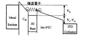
図1は、本発明の第1のトランジスタ素子の一例を示す模式的な断面図である。本発明の第1のトランジスタ素子10は、図1に示すように、エミッタ電極3とコレクタ電極2との間に、半導体層5(5A,5B)とシート状のベース電極4が設けられている。この半導体層5は、詳しくは、コレクタ電極2とベース電極4との間に設けられた第1半導体層5Aと、エミッタ電極3とベース電極4との間に設けられた第2半導体層5Bとを有している。なお、符号1は、基板を表している。こうした形態からなる第1のトランジスタ素子10は、縦型のトランジスタ素子でありながら、グリッドやストライプ等の微細電極のパターニングが必要ないという利点がある。
(First transistor element)
FIG. 1 is a schematic cross-sectional view showing an example of the first transistor element of the present invention. In the
この第1のトランジスタ素子の具体例としては、例えば、厚さ100nmの透明ITO電極をコレクタ電極2とし、その上に、n型有機半導体であるペリレン顔料(Me−PTC、平均厚さ500nm)からなる第1半導体層5Aと、図示しないが酸化ケイ素からなる厚さ2.5nm又は5nmの暗電流抑制層と、アルミニウムからなる平均厚さ20nmのベース電極4と、フラーレン(C60、平均厚さ100nm)からなる第2半導体層5Bと、銀からなる平均厚さ30nmのエミッタ電極3とを、真空蒸着等の成膜手段でその順に積層した。ON電流とOFF電流は、エミッタ電極−コレクタ電極間にコレクタ電圧Vcを5V印加し、さらにエミッタ電極−ベース電極間にベース電圧Vbを印加したときと、印加しないときの、コレクタ電流Ic及びベース電流Ibの変化量を測定して行った。
As a specific example of the first transistor element, for example, a transparent ITO electrode having a thickness of 100 nm is used as the
図2に示すように、ベース電圧Vbが印加されないとき(Vb=0)は、エミッタ電極−コレクタ電極間にほとんど電流が流れないが、ベース電圧Vbの印加によって大幅に電流量が増加し、電流が変調されていることがわかる。そして、図2に示すように、Vc=5V及びVb=3Vのときの電流密度は、350mA/cm2に達しており、この電流密度は例えば有機ELを数千cd/m2発光させるのに十分な大きな電流量である。一般的に、FET構造の場合には、ソース・ドレイン電圧、ゲート電圧ともに数十ボルトを要することからも、本発明に係る第1のトランジスタ素子10が低電圧で大電流変調を実現できていることが容易に理解できる。また、このとき、ベース電極4は半導体層5に対して直接接触しているにもかかわらず、ほとんどベース電極4への電流の流入が起こらない。その結果、図3に示すように、コレクタ電流の変化に対するベース電流の変化の比率、すなわち電流増幅率(hFE)は1を超え、最大で170に達していた。このように本発明の第1のトランジスタ素子は、見かけ上パイポーラトランジスタと同様の電流増幅型のトランジスタ素子として有効に機能することが確認できた。
As shown in FIG. 2, when the base voltage Vb is not applied (Vb = 0), almost no current flows between the emitter electrode and the collector electrode, but the amount of current greatly increases by applying the base voltage Vb. It can be seen that is modulated. As shown in FIG. 2, the current density when Vc = 5 V and Vb = 3 V has reached 350 mA / cm 2 , and this current density is, for example, for causing organic EL to emit several thousand cd / m 2. It is a sufficiently large amount of current. In general, in the case of an FET structure, the source / drain voltage and the gate voltage both require several tens of volts. Therefore, the
すなわち、第1のトランジスタ素子10は、エミッタ電極3とコレクタ電極2との間に半導体層5(5A,5B)が設けられ、且つその半導体層5中にシート状ベース電極4が設けられているので、図2及び図3に示すような本発明の第1のトランジスタ素子10のトランジスタ性能は、エミッタ電極3とコレクタ電極2との間にコレクタ電圧Vcを印加し、さらにエミッタ電極3とベース電極4と間にベース電圧Vbを印加すれば、そのベース電圧Vbの作用により、エミッタ電極3から注入された電荷(電子又は正孔)が著しく加速されてベース電極4を透過し、コレクタ電極2に到達するという原理に基づくものである。すなわち、ベース電圧Vbの印加によってエミッタ電極−コレクタ電極間に流れる電流を増幅させることができる。そして、この第1のトランジスタ素子10では、シート状のベース電極4はベース電圧Vbで加速された弾道電子又は弾道正孔を容易に透過することができる範囲の厚さで全面(図1においては所定の有効幅Wのことである。)に形成されるので、形成された全面で電荷が著しく加速され、しかも加速された電荷がベース電極4を容易に透過することができる。したがって、本発明の第1のトランジスタ素子10によれば、バイポーラトランジスタと同じような電流増幅作用を安定して得ることができる。
That is, in the
以下に、本発明の第1のトランジスタ素子を構成する各層及び各電極について説明する。 Below, each layer and each electrode which comprise the 1st transistor element of this invention are demonstrated.
(基板)
図1においては、基板上に本発明の第1のトランジスタ素子が形成されているが、その基板1の種類や構造は特に限定されるものではなく、積層する各層の材質等により適宜決めることができ、例えば、Al等の金属、ガラス、石英又は樹脂等の各種の材料からなるものを用いることができる。後述する本発明に係る発光素子のように、光を基板1側から出射させるボトムエミッション構造の有機発光素子の場合には、透明又は半透明になる材料で基板が形成されることが好ましいが、光をエミッタ電極3側から出射させるトップエミッション構造の有機発光素子を作製した場合には、必ずしも透明又は半透明になる材料を用いる必要はなく、不透明材料で基板を形成してもよい。
(substrate)
In FIG. 1, the first transistor element of the present invention is formed on a substrate. However, the type and structure of the
特に、有機EL素子の基板として一般的に用いられているもの、すなわち、有機EL素子を強度的に支持しているものを好ましく用いることができる。基板の材質は、用途に応じてフレキシブルな材質や硬質な材質等が選択される。具体的に用いることができる材料としては、例えば、ガラス、石英、ポリエチレン、ポリプロピレン、ポリエチレンテレフタレート、ポリメタクリレート、ポリメチルメタクリレート、ポリメチルアクリレート、ポリエステル、ポリカーボネート等を挙げることができる。また、基板1の形状としては、枚葉状でも連続状でもよく、具体的な形状としては、例えばカード状、フィルム状、ディスク状、チップ状等を挙げることができる。
In particular, a substrate generally used as a substrate for an organic EL element, that is, a substrate that strongly supports the organic EL element can be preferably used. As the material of the substrate, a flexible material, a hard material, or the like is selected according to the application. Specific examples of materials that can be used include glass, quartz, polyethylene, polypropylene, polyethylene terephthalate, polymethacrylate, polymethyl methacrylate, polymethyl acrylate, polyester, and polycarbonate. Further, the shape of the
(電極)
本発明の第1のトランジスタ素子を構成する電極としては、コレクタ電極2、エミッタ電極3及びベース電極4があり、図1に示すように、通常、コレクタ電極2は基板1上に設けられ、ベース電極4は半導体層5(第1半導体層5A及び第2半導体層5B)内に埋め込まれるように設けられ、エミッタ電極3はコレクタ電極2と対向する位置に半導体層5とベース電極4を挟むように設けられる。電極材料としては、金属、導電性酸化物、導電性高分子等の薄膜が用いられる。なお、基板1とコレクタ電極2との間にはバリア層や平滑層等が設けられていてもよい。
(electrode)
As the electrodes constituting the first transistor element of the present invention, there are a
例えば本発明の第1のトランジスタ素子を構成する半導体層5が有機化合物からなる電子輸送層である場合、コレクタ電極2の形成材料としては、例えば、ITO(インジウム錫オキサイド)、酸化インジウム、IZO(インジウム亜鉛オキサイド)、SnO2、ZnO等の透明導電膜、金、クロムのような仕事関数の大きな金属、ポリアニリン、ポリアセチレン、ポリアルキルチオフェン誘導体、ポリシラン誘導体のような導電性高分子等を挙げることができる。一方、エミッタ電極3の形成材料としては、アルミ、銀等の単体金属、MgAg等のマグネシウム合金、AlLi、AlCa、AlMg等のアルミニウム合金、Li、Caをはじめとするアルカリ金属類、それらアルカリ金属類の合金のような仕事関数の小さな金属等を挙げることができる。
For example, when the
一方、本発明の第1のトランジスタ素子を構成する半導体層5が有機化合物からなる正孔輸送層である場合には、上記のコレクタ電極2の形成材料と上記のエミッタ電極3の形成材料とは逆になる。
On the other hand, when the
また、ベース電極4は半導体層5の構成材料とショットキー接触を形成するので、ベース電極4の形成材料としては、上記コレクタ電極2やエミッタ電極3に用いられる電極と同様の電極を挙げることができる。ベース電極4は、エミッタ電極3から供給された電荷をコレクタ電極2側の第1半導体層5A内に強制的に供給するように作用するので、ベース電極4の形成材料としては、必ずしも第1半導体層5Aに電荷を注入し易い材料である必要はない。しかし、コレクタ電極2側の第1半導体層5Aが正孔注入層又は正孔注入材料を有する層である場合には、仕事関数が小さい材料でベース電極4を形成することが好ましく、一方、その第1半導体層5Aが電子注入層又は電子注入材料を有する層である場合には、仕事関数が大きい材料でベース電極4を形成することが好ましい。こうしたベース電極4の形成材料としては、例えば、アルミ、銀等の単体金属、MgAg等のマグネシウム合金、AlLi、AlCa、AlMg等のアルミニウム合金、Li、Caをはじめとするアルカリ金属類、LiF等のアルカリ金属類の合金のような仕事関数の小さな金属等を好ましく使用することができるが、電荷(正孔、電子)注入層とショットキー接触を形成することが可能であれば、ITO(インジウム錫オキサイド)、酸化インジウム、IZO(インジウム亜鉛オキサイド)、SnO2、ZnO等の透明導電膜、金、クロムのような仕事関数の大きな金属、ポリアニリン、ポリアセチレン、ポリアルキルチオフェン誘導体、ポリシラン誘導体のような導電性高分子等も使用することができる。
Further, since the
なお、後述する本発明に係る発光素子のように、光を基板1側から出射させるボトムエミッション構造の有機発光素子の場合には、少なくともコレクタ電極2を透明又は半透明の材料で形成することが好ましく、一方、光をエミッタ電極3側から出射させるトップエミッション構造の有機発光素子を作製する場合には、ベース電極4とエミッタ電極3を透明又は半透明の材料で形成することが好ましい。こうした構成により、光取り出し効率を向上させることができ。透明又は半透明の電極材料としては、ITO(インジウム錫オキサイド)、酸化インジウム、IZO(インジウム亜鉛オキサイド)、SnO2、ZnO等の透明導電膜が好ましく用いられる。
In the case of an organic light emitting device having a bottom emission structure that emits light from the
上記の各電極のうちコレクタ電極2とエミッタ電極3については、真空蒸着、スパッタリング、CVD等の真空プロセスあるいは塗布により形成され、その膜厚は使用する材料等によっても異なるが、例えば10nm〜1000nm程度であることが好ましい。これらの膜厚は、厚さ方向の試料断面を透過型電子顕微鏡(TEM)により5箇所の平均値を測定したものである。
Among the above-mentioned electrodes, the
図4は、ベース電極4の厚さ以外は上記図2及び図3で測定したトランジスタ素子と同じ構成のものを用いた場合において、変調電流量Ic(図4(A))及び電流増幅率hFE(図4(B))の、ベース電極4の膜厚依存性を示したグラフである。また、図5は、ベース電極4の厚さを変化させた際における電流透過率αを示したグラフである。図5に示す電流透過率αは、[Ic(コレクタ電極に到達した電荷)]/[Ic+Ib(エミッタ電極から注入された電荷)]により表される。
FIG. 4 shows the modulation current amount Ic (FIG. 4A) and the current amplification factor h in the case of using the same configuration as the transistor element measured in FIG. 2 and FIG. 3 except for the thickness of the
図4に示すように、変調電流量Ic及び電流増幅率hFEは、いずれもベース電極4が厚くなるのにともなって急激に減少しており、十分なトランジスタ性能を得るためには、薄いベース電極4が必要不可欠であることが分かる。このとき、コレクタ電極2に到達した電荷に対する、エミッタ電極3から注入された電荷の比率である、電流透過率αを算出すると、図5に示すように、ベース電極4の厚さが40nm以下では、99%程度の非常に高い値を示していることが分かった。これは、エミッタ電極3からの電荷がほとんど全てベース電極4を透過していることを意味しており、その結果、パイポーラトランジスタと同様の電流増幅作用が得られているものと考えられる。
As shown in FIG. 4, the modulation current amount Ic and the current amplification factor h FE both decrease rapidly as the
したがって、ベース電極4については、その厚さを40nm以下とすることが好ましいが、図4に示すように、80nm未満とした場合であっても使用可能である。40nm以下の厚さはベース電圧Vbで加速された弾道電子又は弾道正孔を半導体層内に容易に透過させる厚さであるので、シート状のベース電極4の全面で電荷(電子又は正孔)が著しく加速され、しかも加速された電荷がベース電極4を容易に透過することができる。なお、ベース電極4は半導体層5中に切れ目なく(穴やクラック等の欠陥部なく)設けられていればよいので、その厚さの下限は特に限定されないが、通常、1nm程度であればよい。ベース電極4の厚さは、厚さ方向の試料断面を透過型電子顕微鏡により測定した。
Therefore, the thickness of the
図6は、ベース電極4の形成材料を変更した場合の、エミッタ電極3からの注入電流(図6(A))と、コレクタ電極2への到達電流(図6(B))とに対するベース電圧依存性を示すグラフである。なお、このグラフは、ベース電極4の厚さを40nmとした以外は上記図2及び図3で測定したトランジスタ素子と同じ構成のものを用いて測定したものである。図6に示すように、ベース電圧Vbを変化させた場合であっても、エミッタ電極3からの注入電流とコレクタ電極2への到達電流とはほぼ同じであり、電流透過率α[Ic/(Ic+Ib)]は、ベース電極4の材料をLiF/Al、Au、Agとした各試料において、0.99の高確率でベース電極4を透過していることがわかった。
FIG. 6 shows the base voltage with respect to the injection current from the emitter electrode 3 (FIG. 6A) and the current reached to the collector electrode 2 (FIG. 6B) when the material for forming the
また、図6に示すように、ベース電極4の材料をLiF(厚さ0.5nm)/Al(厚さ100nm)、Au(厚さ30nm)、Ag(厚さ30nm)とした各試料を対比すると、電流値の大きさが異なり、LiF/Alが最も高く、Ag、Auの順に低くなっていた。この結果から、ベース電極4の材料により電流値の大きさはことなるが、電流透過率αに対する材料依存性は小さいことがわかった。
In addition, as shown in FIG. 6, the samples in which the
ベース電極4がシート状に設けられ、且つその厚さが所定の厚さ以下である場合に高い電流透過率αを示すメカニズムは必ずしも明確ではないが、現時点では以下のメカニズムが考えられる。
When the
本発明においては、ベース電極4がシート状に設けられている場合(すなわちベース電極4が穴やクラック等の欠陥部を含まない場合)、エミッタ電極3から注入された電荷がシート状のベース電極4全面で加速され、エミッタ電極3から注入された電荷のほとんど全てが弾道電子又は弾道正孔となってベース電極4を透過すると考えられる。その結果、コレクタ電極に到達した電荷の量がエミッタ電極から注入された電荷の量とほぼ同じになって、全体として著しい電流増幅作用を示すと考えられる。一方、本発明者の研究によれば、ベース電極4がシート状に設けられていない試料(すなわちベース電極4が穴やクラック等の欠陥部を含む試料)を作製した場合においては、結果として、コレクタ電極に到達した電荷の量はエミッタ電極から注入された電荷の量よりも少なく、ON/OFF比も小さくなることを確認している。その原因としては、その欠陥部ではエミッタ電極3から注入された電荷を加速できず、その部分の電荷はベース電極4を透過し難くなり、各部位での電流量の増加にムラが生じてしまうと考えられる。
In the present invention, when the
また、ベース電極4が所定の厚さ以下である場合に高い電流透過率αを示すが、これは、エミッタ電極3から注入された電荷がベース電極4を弾道電子又は弾道正孔として透過することによるものと考えられる。つまり、薄いベース電極4が、パイポーラトランジスタのベース層と同じような働き(すなわち、ベースへのキャリア流入を防ぎつつエミッタ電流の増加だけを引き起こすという作用)を受け持つと考え、図7に示すエネルギーダイアグラムを提案する。図7からもわかるように、エミッタ電極−ベース電極間に印加されたベース電圧Vbによって、エミッタ電極3からC60からなる第2半導体層5Bへの電荷注入電流が増大し、その電荷がベース電極4に落ち込むことなく、Me−PCTからなる第1半導体層5Aの伝導帯に高い確率で到達してコレクタ電極2に収集された結果、大きなコレクタ電流変調が得られたものと考えられる。電荷がベース電極4中を弾道的に透過できる距離(電子又は正孔の平均自由行程)は一般的には数nmから数十nm程度と言われているが、これは上記40nm以下の厚さが好ましいという本発明の実験結果とほぼ一致する。
Further, when the
また、ベース電極4を凹凸形状を有するものとすることができる。この凹凸形状を有するベース電極4は、表面粗さが粗いベース電極ということもできるが、こうしたベース電極4は、所定の平均厚さのベース電極を形成した場合であっても薄いところと厚いところを有する。こうした構成からなるベース電極は、電流増幅作用を安定して得ることができる点で好ましい。なお、凹凸形状からなる表面形状は、接触式表面形状測定装置(メーカー:SLOAN THECHNOLOGY、型番:DEKTAK3)又は、AFM(Seiko Instruments, SPI3800)で評価した。
Further, the
例えば、コレクタ電極2とベース電極4との間に設けられた第1半導体層5Aを、結晶性の有機化合物で真空蒸着した場合には、ベース電極4が形成される側の第1半導体層5Aの表面は凹凸形状となっている。そのため、その結晶性の第1半導体層5A上に設けられたベース電極4も凹凸形状で形成される。凹凸形状を有するベース電極4は所定の平均厚さのベース電極4を形成した場合であっても薄いところと厚いところを有するが、本発明によれば、ベース電極4が凹凸形状を有する場合に、電流増幅作用を安定して得ることができる。
For example, when the
結晶性の半導体層を構成する材料としては、上記図2又は図3の結果を示すトランジスタ素子の構成材料である、n型有機半導体であるペリレン顔料(Me−PTC)を好ましく挙げることができる。また、他の材料としては、後述の化学式で示すC60、NTCDA、PTCDA若しくはPh−Et−PTCを挙げることができる。また、これら以外の有機化合物であってもよい。このn型有機半導体であるペリレン顔料(Me−PTC、厚さ400nm)を真空蒸着で形成した際の、ベース電極4側の表面は、X線回折法で測定した結果、明確な結晶性ピークが得られた。また、C60、NTCDA、PTCDA若しくはPh−Et−PTCにおいても、X線回折法で測定した結果、結晶性ピークが得られた。なお、上記図2又は図3の結果を示すトランジスタ素子の結晶性の半導体層5Aの表面粗さはその上に設けられるベース電極4の表面粗さに反映された。したがって、上記図2又は図3の結果を示すトランジスタ素子のベース電極4が所定の表面粗さ(凹凸形状)を有する場合に、電流増幅作用を安定して得ることができることを確認できた。
As a material constituting the crystalline semiconductor layer, a perylene pigment (Me-PTC) which is an n-type organic semiconductor, which is a constituent material of the transistor element showing the results of FIG. 2 or FIG. 3, can be preferably exemplified. Examples of other materials include C60, NTCDA, PTCDA, and Ph-Et-PTC represented by the following chemical formula. Moreover, organic compounds other than these may be sufficient. When the perylene pigment (Me-PTC,
なお、結晶性の半導体層の結晶粒径は、透過型電子顕微鏡で測定でき、その結晶粒径は、ベース電極4の厚さ以上又は厚さ程度の50nm又はそれ以上であった。このように、結晶性の第1半導体層5Aの結晶粒径をベース電極4の厚さ以上となるようにすれば、その第1半導体層5A上にベース電極4を形成することにより、凹凸形状を有するベース電極を容易に形成できる。結晶性の半導体層の表面粗さRzは、AFM(Seiko Instruments, SPI3800)で評価し、Me-PTCでは200nm〜400nm程度であり、NTCDAでは300nm〜500nmであり、C60では50nm〜100nmであった。Rzは、JIS B 0601に準拠した。
Note that the crystal grain size of the crystalline semiconductor layer can be measured with a transmission electron microscope, and the crystal grain size is equal to or larger than the thickness of the
また、ベース電極4が金属からなり、そのベース電極4の片面又は両面にベース電極5の酸化物薄膜が形成されているように構成することもできる。また、半導体層5(5A,5B)上に電極を成膜する場合は、電極成膜時にその半導体層5に加わるダメージを軽減するための保護層(図示しない)を半導体層5上に設けてもよい。保護層としては、例えばAu、Ag、Al等の半透明膜やZnS、ZnSe等の無機半導体膜等の蒸着膜又はスパッタ膜のように、成膜時にダメージを与え難いものが1〜500nm程度の厚さで予め成膜されることが好ましい。
Further, the
(半導体層)
本発明の第1のトランジスタ素子を構成する半導体層5としては、種々の半導体材料を例示でき、通常は電荷輸送特性の良い電荷輸送材料を例示できる。その形態としては、(i)コレクタ電極2とベース電極4との間に設けられた第1半導体層5Aと、エミッタ電極3とベース電極4との間に設けられた第2半導体層5Bとが、異なる半導体材料で形成されていること、(ii)第1半導体層5A及び第2半導体層5Bが正孔輸送材料又は電子輸送材料で形成されてなること、(iii)エミッタ電極3とベース電極4との間又はコレクタ電極2とベース電極4との間に設けられた半導体層5A,5Bのいずれもが、有機化合物で形成されていること、(iv)コレクタ電極2とベース電極4との間に設けられた第1半導体層5Aの厚さT1と、エミッタ電極3とベース電極4との間に設けられた第2半導体層5Bの厚さT2との比(T1/T2)が、1/1〜10/1の範囲内であること、好ましくは3/1〜7/1の範囲内であること、(v)エミッタ電極3と、エミッタ電極3に隣接する第2半導体層5Bとの間に、電荷注入層を有すること、又は、(vi)その電荷注入層が、LiF、Ca等のアルカリ金属又はその化合物で形成されていること、が好ましい。
(Semiconductor layer)
As the
半導体層5(5A,5B)の形成材料としては、後述の実験例で用いたAlq3、C60、NTCDA、PTCDA、Me−PTC、若しくはPh−Et−PTCを挙げることができ、また、アントラキノジメタン、フルオレニリデンメタン、テトラシアノエチレン、フルオレノン、ジフェノキノンオキサジアゾール、アントロン、チオピランジオキシド、ジフェノキノン、ベンゾキノン、マロノニトリル、ニジトロベンゼン、ニトロアントラキノン、無水マレイン酸若しくはペリレンテトラカルボン酸、又はこれらの誘導体等、電荷輸送材料として通常使用されるものを用いることができる。また、コレクタ電極2とベース電極4との間に設けられた第1半導体層5Aにおいては、後述する本発明の発光素子の説明欄で列記した発光層形成材料を用いてもよい。
Examples of the material for forming the semiconductor layer 5 (5A, 5B) include Alq 3 , C60, NTCDA, PTCDA, Me-PTC, and Ph-Et-PTC used in the experimental examples described later. Anthraquino Dimethane, fluorenylidenemethane, tetracyanoethylene, fluorenone, diphenoquinone oxadiazole, anthrone, thiopyran dioxide, diphenoquinone, benzoquinone, malononitrile, niditrobenzene, nitroanthraquinone, maleic anhydride or perylenetetracarboxylic acid, Or what is normally used as charge transport materials, such as these derivatives, can be used. In the
半導体層5(5A,5B)の電荷移動度は、なるべく高いことが望ましく、少なくとも、0.001cm2/Vs以上であることが望ましい。また、コレクタ電極2側の第1半導体層5Aの厚さは、通常、300nm〜1000nm程度を挙げることができるが、好ましくは400nm〜700nm程度である。なお、その厚さが300nm未満の場合又は1000nmを超える場合は、トランジスタ動作を生じないことがある。一方、エミッタ電極3側の第2半導体層5Bの厚さは、通常、500nm程度以下を挙げることができるが、好ましくは50nm〜150nm程度である。なお、その厚さが50nm未満の場合は、導通の問題が発生して歩留まりが低下することがある。
The charge mobility of the semiconductor layer 5 (5A, 5B) is desirably as high as possible, and is preferably at least 0.001 cm 2 / Vs. The thickness of the
コレクタ電極2とベース電極4との間に設けられる第1半導体層5Aの形成材料として、下記の各有機化合物を用いて実験を行った。実験は、厚さ100nmの透明ITO電極をコレクタ電極2とし、その上に、下記の5種の化合物(Alq3、C60、NTCDA、PTCDA、Me−PTC)から選択した1種からなる第1半導体層5Aと、アルミニウムからなる平均厚さ20nmのベース電極4と、フラーレン(C60、平均厚さ100nm)からなる第2半導体層5Bと、銀からなる平均厚さ30nmのエミッタ電極3とを、真空蒸着等の成膜手段でその順に積層したトランジスタ素子を用いた。第1半導体層5Aの厚さは、Alq3、C60においては100nmとし、NTCDA、PTCDA、Me−PTCにおいては100nmとした。
Experiments were performed using the following organic compounds as a material for forming the
こうして作製した5種のトランジスタ素子について、コレクタ電圧Vcを5Vとし、ベース電圧Vbを0V〜3Vの範囲で変調させた。出力変調特性の測定は、図2及び図3の場合と同様、エミッタ電極−コレクタ電極間にコレクタ電圧Vcを印加し、さらにエミッタ電極−ベース電極間にベース電圧Vbを印加した時の、コレクタ電流Ic及びベース電流Ibの変化量を測定して行った。また、コレクタ電流の変化に対するベース電流の変化の比率、すなわち電流増幅率(hFE)を算出した。表1は、その結果を示している。 For the five types of transistor elements thus fabricated, the collector voltage Vc was set to 5 V, and the base voltage Vb was modulated in the range of 0 V to 3 V. As in the case of FIGS. 2 and 3, the output modulation characteristic is measured by applying a collector voltage Vc between the emitter electrode and the collector electrode and further applying a collector voltage Vb between the emitter electrode and the base electrode. The measurement was performed by measuring the amount of change in Ic and base current Ib. Further, the ratio of the change in the base current to the change in the collector current, that is, the current amplification factor (h FE ) was calculated. Table 1 shows the results.

表1に示すように、C60からなる第2半導体層5Bに対して、Alq3やC60からなる第1半導体層5Aを形成した場合には、十分な結果を得ることができなかった。また、NTCDAやPTCDAからなる第1半導体層5Aを形成した場合の電流増幅率(hFE)は、電流増幅が認められ、それぞれ15、46であった。一方、Me−PTCからなる第1半導体層5Aを形成した場合の電流増幅率(hFE)は、200という著しく高い値を示した。このように、本発明の第1のトランジスタ素子を構成する半導体層5(5A,5B)には、電荷輸送材料を用いることができるが、詳細には、材料の組み合わせにより高い電流増幅作用を生じさせることができる。そして、その組み合わせは、現時点では、図7に示すように、半導体材料のLUMOの位置が関係していると考えられるので、その点を考慮して組み合わせることが望ましい。
As shown in Table 1, the
表1には、コレクタ電圧Vcを5Vとし、ベース電圧VbのON電圧を3V、OFF電圧を0Vとしたときの、ON/OFF比の測定結果も併せて示した。表1に示したように、ON/OFF比は、NTCDAやPTCDAからなる第1半導体層5Aを形成した場合は、大きな値となり、それぞれ40、20であった。一方、Me−PTCからなる第1半導体層5Aを形成した場合のON/OFF比は、100という著しく高い値を示した。
Table 1 also shows the measurement result of the ON / OFF ratio when the collector voltage Vc is 5 V, the ON voltage of the base voltage Vb is 3 V, and the OFF voltage is 0 V. As shown in Table 1, the ON / OFF ratio was large when the
このように本発明の第1のトランジスタ素子は、見かけ上パイポーラトランジスタと同様の電流増幅型のトランジスタ素子として有効に機能することが確認できた。 As described above, it was confirmed that the first transistor element of the present invention apparently functions effectively as a current amplification type transistor element similar to the bipolar transistor.
(第2のトランジスタ素子)
次に、本発明の第2のトランジスタ素子について説明する。図8は、本発明の第2のトランジスタ素子の一例を示す模式的な断面図であり、図9は、本発明の第2のトランジスタ素子の他の一例を示す模式的な断面図である。本発明の第2のトランジスタ素子20,30は、エミッタ電極3とコレクタ電極2との間に、半導体層5とシート状のベース電極4が設けられたトランジスタ素子であって、少なくともエミッタ電極3とベース電極4との間又はコレクタ電極2とベース電極4との間に、暗電流抑制層6,7が設けられている。図8においては、コレクタ電極2とベース電極4との間に暗電流抑制層6が設けられており、図9においては、コレクタ電極2とベース電極4との間に暗電流抑制層6が設けられ、さらにエミッタ電極3とベース電極4との間にも暗電流抑制層7が設けられている。なお、第2のトランジスタ素子は、上記第1のトランジスタ素子と比較して、暗電流抑制層が設けられている点が異なりその他の点は上記第1のトランジスタ素子と同じであるので、図8及び図9並びに以下の説明においては、同一の符号を用いてその説明を省略する。また、図8及び図9では基板は省略して図示している。
(Second transistor element)
Next, the second transistor element of the present invention will be described. FIG. 8 is a schematic cross-sectional view showing an example of the second transistor element of the present invention, and FIG. 9 is a schematic cross-sectional view showing another example of the second transistor element of the present invention. The
図10は、図8の第2のトランジスタ素子20の場合におけるON電流とOFF電流の経路を示したものであり、図11は、図9の第2のトランジスタ素子30の場合におけるON電流とOFF電流の経路を示したものである。これらの第2のトランジスタ素子20,30は、上記第1のトランジスタ素子10のエミッタ電極−コレクタ電極間に例えば5Vのコレクタ電圧Vcを印加したとき、エミッタ電極−ベース電極間に小さいベース電圧Vbを印加した場合又はベース電圧Vbを印加しない場合(Vb=0V)にベース電極−コレクタ電極間に動作に必要な電流成分以外の漏れ電流が流れ、ON/OFF比が低下することがあるという問題を解決したものである、そして、上記のように、半導体層5中に形成された薄いシート状のベース電極4の一方又は両面に暗電流抑制層(6,7)を形成することにより、動作に必要な漏れ電流を抑制してON/OFF比を向上させたトランジスタ素子である。
FIG. 10 shows the path of the ON current and the OFF current in the case of the
本発明の第2のトランジスタ素子20,30によれば、図10及び図11に示すように、少なくともエミッタ電極3とベース電極4との間又はコレクタ電極2とベース電極4との間に暗電流抑制層(6,7)が設けられているので、その暗電流抑制層により、エミッタ電極−ベース電極間に小さい電圧Vbを印加した場合又は電圧Vbを印加しない場合に、ベース電極−コレクタ電極間にトランジスタ動作に暗電流が流れるのを効果的に抑制することができ、その結果、ON/OFF比を向上させることができる。なお、暗電流抑制層6,7は、例えばエミッタ電極−ベース電極間に電圧Vbを印加しない場合の暗電流は効果的に抑制できるが、エミッタ電極−ベース電極間に電圧Vbを印加した場合のいわゆるON電流はあまり妨げないものを用いることが望ましい。
According to the
暗電流抑制層6,7は、ベース電圧VbをOFFにした際に、コレクタ電圧Vcによって生じたエミッタ電流がベース電極4を透過しないように作用するので、図8に示すように少なくともコレクタ電極2とベース電極4との間に設けられる。なお、必要に応じてベース電極4の両面に暗電流抑制層7を設けることができる。また、形成する暗電流抑制層は、ベース電極4に隣接して(すなわち、ベース電極4に接触するように)設けられていることが好ましい。
Since the dark current suppressing
暗電流抑制層としては、ベース電極4に一様に形成されていることが好ましい。ここで、「一様に」とは、穴や切れ目がなく全面に形成されていることをいう。暗電流抑制層の厚さが薄すぎると、一様な暗電流抑制層を成膜し難いという難点があり、暗電流抑制層の厚さが厚すぎると、ベース電圧VbをON状態にしたときの電流も顕著に抑制されることがある。
The dark current suppressing layer is preferably formed uniformly on the
暗電流抑制層の形成材料としては、有機系絶縁層や無機系絶縁層を挙げることができるが、上記厚さで成膜できることと暗電流抑制層としての作用効果を奏することを条件に以下の具体例を挙げることができる。例えば、SiO2、SiNx、A12O3等の無機材料や、ポリクロロピレン、ポリエチレンテレフタレート、ポリオキシメチレン、ポリビニルクロライド、ポリフッ化ビニリデン、シアノエチルプルラン、ポリメチルメタクリレート、ポリビニルフェノール、ポリサルホン、ポリカーボネート、ポリイミド等の有機材料等を挙げることができる。なお、これらの形成材料は、単独で用いてもよいし、2種以上の材料を用いてもよい。 Examples of the material for forming the dark current suppressing layer include an organic insulating layer and an inorganic insulating layer. The following conditions are provided on condition that the film can be formed with the above-mentioned thickness and that the effect as the dark current suppressing layer is achieved. Specific examples can be given. For example, inorganic materials such as SiO 2 , SiN x , A1 2 O 3 , polychloropyrene, polyethylene terephthalate, polyoxymethylene, polyvinyl chloride, polyvinylidene fluoride, cyanoethyl pullulan, polymethyl methacrylate, polyvinyl phenol, polysulfone, polycarbonate, polyimide And organic materials such as In addition, these formation materials may be used independently and may use 2 or more types of materials.
また、暗電流抑制層の形成材料として、有機系半導体材料を用いてもよいし、無機系半導体材料を用いてもよい。これらの材料から、上記厚さで成膜できることと暗電流抑制層としての作用効果を奏することを条件に最適なものが選定される。これらの形成材料も上記同様、単独で用いてもよいし、2種以上の材料を用いてもよい。 In addition, as a material for forming the dark current suppressing layer, an organic semiconductor material or an inorganic semiconductor material may be used. From these materials, an optimum material is selected on the condition that the film can be formed with the above-mentioned thickness and that the effect of the dark current suppressing layer can be obtained. These forming materials may also be used alone, or two or more materials may be used as described above.
図12は、暗電流抑制層として酸化ケイ素膜を形成した場合でのON電流と、ON/OFF比の実験結果を示すグラフである。実験は、厚さ100nmの透明ITO電極をコレクタ電極2とし、その上に、Me−PTCからなる第1半導体層5A(厚さ400nm)と、アルミニウムからなる平均厚さ20nmのベース電極4と、フラーレン(C60、平均厚さ100nm)からなる第2半導体層5Bと、銀からなる平均厚さ30nmのエミッタ電極3とを、真空蒸着等の成膜手段でその順に積層したトランジスタ素子を用いた。なお、比較試料として、酸化ケイ素を設けないトランジスタ素子を作製した。
FIG. 12 is a graph showing the ON current and the ON / OFF ratio experimental results when a silicon oxide film is formed as the dark current suppressing layer. In the experiment, a transparent ITO electrode having a thickness of 100 nm is used as the
前記の試料について、ON電流とOFF電流を測定した。測定は、エミッタ電極−コレクタ電極間にコレクタ電圧Vcを5V印加し、さらにエミッタ電極−ベース電極間にベース電圧Vbを印加したときに測定したコレクタ電流をON電流とし、印加しないときに測定したコレクタ電流をOFF電流とした。図12に示したように、暗電流抑制層である酸化ケイ素の厚さが5nmのときのON/OFF比は、約250であった。なお、このときのON電流は、酸化ケイ素膜を設けないときに比べて低下していたものの、厚さ2.5nmの酸化ケイ素膜を設けた場合と比べてあまり変化がなかった。こうしたことは、ON電流をあまり低下させずにON/OFFを向上させることができるので好ましい。 For the sample, the ON current and OFF current were measured. In the measurement, a collector voltage Vc of 5 V is applied between the emitter electrode and the collector electrode, and the collector current measured when the base voltage Vb is applied between the emitter electrode and the base electrode is set as the ON current, and the collector measured when not applied. The current was OFF current. As shown in FIG. 12, the ON / OFF ratio was about 250 when the thickness of the silicon oxide serving as the dark current suppressing layer was 5 nm. In addition, although the ON current at this time was lower than that when the silicon oxide film was not provided, there was not much change compared with the case where the silicon oxide film having a thickness of 2.5 nm was provided. This is preferable because ON / OFF can be improved without significantly reducing the ON current.
図13及び図14は、暗電流抑制層を自然酸化により形成した場合のコレクタ電流の経時変化を示したものであり、図13は、暗電流抑制層が形成されていない場合のコレクタ電流のグラフを示したものであり、図14は、暗電流抑制層を自然酸化により形成した後のコレクタ電流のグラフを示したものである。実験は、厚さ100nmの透明ITO電極をコレクタ電極2とし、その上に、Me−PTCからなる平均厚さ400nmの第1半導体層5Aと、アルミニウムからなる平均厚さ20nmのベース電極4と、フラーレン(C60、平均厚さ100nm)からなる第2半導体層5Bと、銀からなる平均厚さ30nmのエミッタ電極3とを、真空蒸着等の成膜手段でその順に積層したトランジスタ素子を用いた。
FIGS. 13 and 14 show changes with time in the collector current when the dark current suppression layer is formed by natural oxidation, and FIG. 13 is a graph of the collector current when the dark current suppression layer is not formed. FIG. 14 shows a graph of the collector current after the dark current suppression layer is formed by natural oxidation. In the experiment, a transparent ITO electrode having a thickness of 100 nm was used as the
前記の試料について、エミッタ電極−コレクタ電極間にコレクタ電圧Vcを0V〜5Vまで印加し、さらにエミッタ電極−ベース電極間にベース電圧Vbを3V印加した場合と4V印加した場合に測定したコレクタ電流をON電流とし、印加しないときに測定したコレクタ電流をOFF電流とした。図13の結果は、上記トランジスタ素子を形成した直後に測定したものであり、ベース電極4の両面には暗電流抑制層6,7は生じていない場合のものである。一方、図14の結果は、上記トランジスタ素子を形成し、温度20〜25℃、湿度30〜70%の室内での大気環境中に37分間放置した後に測定したものであり、ベース電極4の両面には酸化アルミニウムからなる暗電流抑制層6,7が生じていた。このときの酸化アルミニウムは、アルミニウムからなるベース電極4の自然酸化膜であり、TEMによる厚さ測定により確認した。
For the above sample, the collector voltage Vc applied between 0 V and 5 V between the emitter electrode and the collector electrode, and the collector current measured when the base voltage Vb was applied between 3 V and 4 V between the emitter electrode and the base electrode were measured. The collector current measured when the current was not applied was set as the OFF current. The result of FIG. 13 is measured immediately after the transistor element is formed, and is when the dark current suppression layers 6 and 7 are not formed on both surfaces of the
図13において、コレクタ電圧Vcが5Vで、ベース電圧Vbが0VのときのOFF電流は2.89mA/cm2であったのに対し、図14において、コレクタ電圧Vcが5Vで、ベース電圧Vbが0VのときのOFF電流は0.0025mA/cm2であり、ON/OFF比は、図13での36から、図14での330にまで著しく向上した。図15は、上記のように温度20〜25℃、湿度30〜70%の室内での大気環境中に放置した時間と、ON/OFF比の関係である。ON/OFF比は、放置時間が20分までは顕著に向上し、20分経過後に300を超える高い値で安定した。なお、酸化アルミニウム膜の厚さは、時間の経過とともに厚くなることが確認され、放置時間20分のときの酸化アルミニウムの厚さよりも、放置時間37分のときの酸化アルミニウムの厚さが厚かった。こうした結果は、上記図12での実験と合わせて考えれば、主にコレクタ電極2側に設けられた酸化アルミニウム膜の作用効果によるものと考えられる。
In FIG. 13, when the collector voltage Vc is 5 V and the base voltage Vb is 0 V, the OFF current is 2.89 mA / cm 2 , whereas in FIG. 14, the collector voltage Vc is 5 V and the base voltage Vb is The OFF current at 0 V was 0.0025 mA / cm 2 , and the ON / OFF ratio was significantly improved from 36 in FIG. 13 to 330 in FIG. FIG. 15 shows the relationship between the ON / OFF ratio and the time of leaving in the indoor air environment at a temperature of 20 to 25 ° C. and a humidity of 30 to 70% as described above. The ON / OFF ratio was remarkably improved until the standing time was 20 minutes, and stabilized at a high value exceeding 300 after 20 minutes. The thickness of the aluminum oxide film was confirmed to increase with time, and the thickness of the aluminum oxide at the standing time of 37 minutes was larger than the thickness of the aluminum oxide at the standing time of 20 minutes. . Considering this result together with the experiment in FIG. 12, it can be considered that this result is mainly due to the effect of the aluminum oxide film provided on the
この第2のトランジスタ素子におけるその他の構成、すなわち、各電極の形成材料や半導体層の形成材料等は、上記第1のトランジスタ素子の欄で説明したものと同じである。 Other configurations of the second transistor element, that is, the formation material of each electrode, the formation material of the semiconductor layer, and the like are the same as those described in the column of the first transistor element.
(トランジスタ素子の製造方法)
本発明のトランジスタ素子の製造方法は、上記第2のトランジスタ素子の製造方法に係るものであって、エミッタ電極3とコレクタ電極2との間に半導体層5(5A,5B)及びシート状のベース電極4が設けられ、少なくともエミッタ電極3とベース電極4との間又はコレクタ電極2とベース電極4との間に暗電流抑制層(6,7)を形成する方法である。そして、その特徴は、ベース電極4を化学反応させることにより、暗電流抑制層を形成する。こうした化学反応としては、図12〜図14の実験結果のところで示したように、ベース電極4を形成した後に該ベース電極4の一部(半導体層側に接する側の面)を酸化させて暗電流抑制層(6,7)を形成する方法、又は、ベース電極4を形成した後に該ベース電極4を加熱処理して暗電流抑制層(6,7)を形成する方法、を挙げることができる。こうした方法により、暗電流抑制層(6,7)を容易に形成することができ、漏れ電流を抑制してON/OFF比を向上させたトランジスタ素子を容易に提供することができる。
(Manufacturing method of transistor element)
The method for manufacturing a transistor element according to the present invention relates to the method for manufacturing the second transistor element, and includes a semiconductor layer 5 (5A, 5B) and a sheet-like base between the
なお、暗電流抑制層をコレクタ電極2側にのみ設ける場合には、第1半導体層5A上にベース電極4を形成した後、そのベース電極4上に酸化等の化学反応を防止することを目的の保護層を設ければ、上暗電流抑制層をコレクタ電極2側にのみ、ベース電極4の自然酸化膜もしくは加熱酸化膜を設けることができる。
In the case where the dark current suppressing layer is provided only on the
(電子デバイス)
本発明の電子デバイスは、上記本発明の第1のトランジスタ素子をスイッチング素子として有するもの、又は、上記本発明の第2のトランジスタ素子をスイッチング素子として有するもの、であることが好ましい。本発明は、第1又は第2のトランジスタ素子をスイッチング素子として、例えば有機EL素子と組み合わせた電子デバイスとすることができる。第1又は第2のトランジスタ素子が低電圧で大電流変調が可能であることから、例えば有機ELのスイッチング素子である駆動トランジスタとして好ましく組み合わせてなる電子デバイスを提供できる。
(Electronic device)
The electronic device of the present invention is preferably one having the first transistor element of the present invention as a switching element or one having the second transistor element of the present invention as a switching element. The present invention can be an electronic device combining the first or second transistor element as a switching element, for example, an organic EL element. Since the first or second transistor element can perform a large current modulation at a low voltage, an electronic device preferably combined as a drive transistor that is a switching element of an organic EL, for example, can be provided.
本発明のトランジスタ素子をn型トランジスタとして用いる場合において、ベース電極4とコレクタ電極2との間に有機EL層を設け、ベース電極4を陰極として用いて電子デバイスを構成すれば、従来のように電子を注入し易いが酸化し易いアルカリ金属を陰極として用いなくても、有機EL層を構成する電荷輸送層中に電荷を効果的に注入することができるという優れた効果を奏する。
When the transistor element of the present invention is used as an n-type transistor, an organic EL layer is provided between the
(発光素子)
次に、発光素子について説明する。図16は、第1のトランジスタ素子のベース電極4とコレクタ電極2との間に有機EL層41を有し、その有機EL層41が少なくとも発光層42を1層以上含む発光素子40の一例を示す模式断面図である。この第1の発光素子40は、図16に示すように、例えば厚さ100nmの透明ITO電極をコレクタ電極2とし、その上に、CuPcからなる厚さ2nmの正孔注入層44と、NPDからなる厚さ30nmの正孔輸送層43と、Alq3からなる厚さ30nmの発光層42と、BCPからなる厚さ10nmの励起子ブロック層45と、n型有機半導体のペリレン顔料(Me−PTC、厚さ500nm)からなる電子輸送性の第1半導体層5Aと、アルミニウムからなる厚さ20nmのベース電極4と、フラーレン(C60、厚さ100nm)からなる第2半導体層5Bと、銀からなる厚さ30nmのエミッタ電極3とを、真空蒸着等の成膜手段でその順に積層したものである。
(Light emitting element)
Next, a light emitting element will be described. FIG. 16 shows an example of a
また、図17は、第2のトランジスタ素子のベース電極4とコレクタ電極2との間に有機EL層41を有し、その有機EL層41が少なくとも発光層42を1層以上含む発光素子50の一例を示す模式断面図である。この第2の発光素子40は、図17に示すように、第1半導体層5Aとベース電極4との間に、酸化ケイ素からなる厚さ5nmの暗電流抑制層6を形成した他は、上記第1の発光素子40と同じ構成である。
FIG. 17 also shows an
なお、図16及び図17に示す本発明の発光素子40,50のトランジスタとしての構成は、上記第1及び第2のトランジスタ素子の基本的な構成と同じであるので、既に説明した同じ構成については、同一の符号を用いて詳しい説明を省略する。また、図16及び図17に示す発光素子40,50を構成する有機EL層の構成材料の化学式を以下に示す。
The configuration of the
図18は、図16に示す構成の発光素子の実験例であり、コレクタ電圧Vcとして一定の電圧を印加しながらベース電圧Vbを変化させたときのEL輝度の変化を示すグラフである。図18に示すように、ベース電圧Vbの印加によって有機EL層にかかる電圧は減少しているにもかかわらず、EL輝度は増大し、Vc=12V、Vb=2.5Vの低電圧で、約100cd/m2の輝度の変調を達成した。 FIG. 18 is an experimental example of the light emitting device having the configuration shown in FIG. 16, and is a graph showing a change in EL luminance when the base voltage Vb is changed while a constant voltage is applied as the collector voltage Vc. As shown in FIG. 18, although the voltage applied to the organic EL layer is decreased by the application of the base voltage Vb, the EL luminance is increased, and at a low voltage of Vc = 12V and Vb = 2.5V, A luminance modulation of 100 cd / m 2 was achieved.
このように、本発明の発光素子は、トランジスタ素子の第1半導体層5Aとコレクタ電極2との間に有機EL層41を有し、全体としてその有機EL層41と同様の面状の積層構造となるので、面状の電流を変調できる。こうした構造の発光素子は、駆動素子であるトランジスタ素子と、有機EL素子を一度に作製できるだけでなく、駆動トランジスタの占有面積が実質ゼロとなることから開口率を大きくできるというメリットがある。近年において、有機FET構造でも発光が観測されるようになったが、まだその性能は低く、実用的な性能を示す有機発光トランジスタとしては、縦型の有機SITを用いたものが知られている。本発明の発光素子は、コレクタ電極2側に有機EL層を積層するだけで電流変調可能な発光素子を実現できた。しかも、本発明の発光素子は、中間電極等の微細パターニングが不必要であり、極めて実用的である。
As described above, the light emitting device of the present invention has the
有機EL層41は、上記のように、少なくとも1層以上の発光層42を有し、さらに、正孔注入層44、正孔輸送層43、電子輸送層、及び電子注入層から選ばれる1又は2以上の層を有することが好ましい。図16及び図17の例では、発光層42のコレクタ電極2側に正孔輸送層43と正孔注入層44が設けられている。また、発光層42のベース電極4側には励起子ブロック層45が設けられている。この発光素子40,50はトランジスタ素子により多くの電荷が加速されて有機EL層41の発光層42に到達するので、ベース電極4からの電荷の注入は容易である。したがって、有機EL層41は必ずしも電荷注入層を有していなくてもよいという利点がある。そのため、従来のように電子を注入し易いが酸化し易いアルカリ金属を陰極として用いなくてもよいという効果がある。
As described above, the
発光層42の形成材料としては、有機EL素子の発光層として一般的に用いられている材料であれば特に限定されず、例えば色素系発光材料、金属錯体系発光材料、高分子系発光材料等を挙げることができる。
The material for forming the
色素系発光材料としては、例えば、シクロペンタジエン誘導体、テトラフェニルブタジエン誘導体、トリフェニルアミン誘導体、オキサジアゾール誘導体、ピラゾロキノリン誘導体、ジスチリルベンゼン誘導体、ジスチリルアリーレン誘導体、シロール誘導体、チオフェン環化合物、ピリジン環化合物、ペリノン誘導体、ペリレン誘導体、オリゴチオフェン誘導体、トリフマニルアミン誘導体、オキサジアゾールダイマー、ピラゾリンダイマー等を挙げることができる。 Examples of dye-based light-emitting materials include cyclopentadiene derivatives, tetraphenylbutadiene derivatives, triphenylamine derivatives, oxadiazole derivatives, pyrazoloquinoline derivatives, distyrylbenzene derivatives, distyrylarylene derivatives, silole derivatives, thiophene ring compounds, Examples thereof include pyridine ring compounds, perinone derivatives, perylene derivatives, oligothiophene derivatives, trifumanylamine derivatives, oxadiazole dimers, and pyrazoline dimers.
金属錯体系発光材料としては、例えば、アルミキノリノール錯体、ベンゾキノリノールベリリウム錯体、ベンゾオキサゾール亜鉛錯体、ベンゾチアゾール亜鉛錯体、アゾメチル亜鉛錯体、ポルフィリン亜鉛錯体、ユーロピウム錯体等、中心金属に、Al、Zn、Be等、又はTb、Eu、Dy等の希土類金属を有し、配位子にオキサジアゾール、チアジアゾール、フェニルピリジン、フェニルベンゾイミダゾール、キノリン構造等を有する金属錯体等を挙げることができる。 Examples of the metal complex light emitting material include aluminum quinolinol complex, benzoquinolinol beryllium complex, benzoxazole zinc complex, benzothiazole zinc complex, azomethylzinc complex, porphyrin zinc complex, europium complex, etc. Or a metal complex having a rare earth metal such as Tb, Eu, or Dy and having a oxadiazole, thiadiazole, phenylpyridine, phenylbenzimidazole, quinoline structure, or the like as a ligand.
高分子系発光材料としては、例えば、ポリパラフェニレンビニレン誘導体、ポリチオフェン誘導体、ポリパラフェニレン誘導体、ポリシラン誘導体、ポリアセチレン誘導体、ポリビニルカルバゾール、ポリフルオレノン誘導体、ポリフルオレン誘導体、ポリキノキサリン誘導体、及びそれらの共重合体等を挙げることができる。 Examples of the polymer light-emitting material include polyparaphenylene vinylene derivatives, polythiophene derivatives, polyparaphenylene derivatives, polysilane derivatives, polyacetylene derivatives, polyvinylcarbazole, polyfluorenone derivatives, polyfluorene derivatives, polyquinoxaline derivatives, and co-polymers thereof. A coalescence etc. can be mentioned.
発光層42中には、発光効率の向上や発光波長を変化させる等の目的でドーピング剤等の添加剤を添加するようにしてもよい。ドーピング剤としては、例えば、ペリレン誘導体、クマリン誘導体、ルブレン誘導体、キナクリドン誘導体、スクアリウム誘導体、ポルフィリン誘導体、スチリル色素、テトラセン誘導体、ピラゾリン誘導体、デカシクレン、フェノキサゾン、キノキサリン誘導体、カルバゾール誘導体、フルオレン誘導体等を挙げることができる。
An additive such as a doping agent may be added to the
正孔輸送層43の形成材料としては、フタロシアニン、ナフタロシアニン、ポリフィリン、オキサジアゾール、トリフェニルアミン、トリアゾール、イミダゾール、イミダゾロン、ピラゾリン、テトラヒドロイミダゾール、ヒドラゾン、スチルベン、ペンタセン、ポリチオフェン若しくはブタジエン、又はこれらの誘導体等、正孔輸送材料として通常使用されるものを用いることができる。また、正孔輸送層43の形成材料として市販されている、例えばポリ(3、4)エチレンジオキシチオフェン/ポリスチレンスルホネート(略称PEDOT/PSS、バイエル社製、商品名;Baytron P AI4083、水溶液として市販。)等も使用することができる。正孔輸送層43は、こうした化合物を含有した正孔輸送層形成用塗液を用いて形成される。なお、これらの正孔輸送材料は、上記の発光層42内に混ぜてもよいし、正孔注入層44内に混ぜてもよい。
As a forming material of the
また、図16及び図17では、Me−PTCからなる第1半導体層5Aが電子輸送性の層であるので、別個に電子輸送層として設けていないが、必要に応じて発光層42のベース電極4側に設けてもよい。電子輸送層の形成材料としては、アントラキノジメタン、フルオレニリデンメタン、テトラシアノエチレン、フルオレノン、ジフェノキノンオキサジアゾール、アントロン、チオピランジオキシド、ジフェノキノン、ベンゾキノン、マロノニトリル、ニジトロベンゼン、ニトロアントラキノン、無水マレイン酸若しくはペリレンテトラカルボン酸、又はこれらの誘導体等、電子輸送材料として通常使用されるものを用いることができる。電子輸送層は、こうした化合物を含有した電子輸送層形成用塗液を用いて形成される。なお、これらの電子輸送材料は、上記の発光層42内に混ぜてもよいし、電子注入層内に混ぜてもよい。
In FIG. 16 and FIG. 17, the
正孔注入層44の形成材料としては、例えば、発光層42の発光材料に例示した化合物の他、フェニルアミン系、スターバースト型アミン系、フタロシアニン系、酸化バナジウム、酸化モリブデン、酸化ルテニウム、酸化アルミニウムなどの酸化物、アモルファスカーボン、ポリアニリン、ポリチオフェンなどの誘導体等を挙げることができる。
As a material for forming the
図16及び図17には含まれないが、必要であれば電子注入層を設けてもよい。電子注入層の形成材料としては、発光層の発光材料に例示した化合物の他、アルミニウム、フッ化リチウム、ストロンチウム、酸化マグネシウム、フッ化マグネシウム、フッ化ストロンチウム、フッ化カルシウム、フッ化バリウム、酸化アルミニウム、酸化ストロンチウム、カルシウム、ポリメチルメタクリレートポリスチレンスルホン酸ナトリウム、リチウム、セシウム、フッ化セシウム等のようにアルカリ金属類、及びアルカリ金属類のハロゲン化物、アルカリ金属の有機錯体等を挙げることができる。 Although not included in FIGS. 16 and 17, an electron injection layer may be provided if necessary. As a material for forming the electron injection layer, aluminum, lithium fluoride, strontium, magnesium oxide, magnesium fluoride, strontium fluoride, calcium fluoride, barium fluoride, aluminum oxide in addition to the compounds exemplified as the light emitting material of the light emitting layer Strontium oxide, calcium, sodium polymethyl methacrylate polystyrene sulfonate, lithium, cesium, cesium fluoride and the like, alkali metals, alkali metal halides, alkali metal organic complexes, and the like.
なお、上述した発光層や電荷輸送層等の有機層中には、必要に応じてオリゴマー材料又はデンドリマー材料の発光材料若しくは電荷輸送注入材料を含有させてもよい。 In addition, in the organic layers such as the light-emitting layer and the charge transport layer described above, a light-emitting material of an oligomer material or a dendrimer material or a charge transport injection material may be included as necessary.
上述した各層は、真空蒸着法によって成膜するか、あるいは、それぞれの形成材料をトルエン、クロロホルム、ジクロロメタン、テトラヒドロフラン、ジオキサン等の溶媒に溶解又は分散させて塗布液を調整し、その塗布液を塗布装置等を用いて塗布又は印刷等することで形成される。 Each of the above layers is formed by a vacuum deposition method, or each forming material is dissolved or dispersed in a solvent such as toluene, chloroform, dichloromethane, tetrahydrofuran, dioxane or the like to prepare a coating solution, and the coating solution is applied. It is formed by coating or printing using an apparatus or the like.
励起子ブロック層45は、正孔ブロック層、電子ブロック層等として機能する層であり、キャリア(正孔、電子)のつきぬけを防止し、効率よくキャリアの再結合させるためのブロック層である。図16及び図17においては、トランジスタ素子がn型半導体材料で構成されているので、コレクタ電極2が陽極として作用する。その結果、コレクタ電極2から正孔が注入されるので、発光層42のベース電極4側の隣接面には正孔ブロック層としての励起子ブロック層45を形成することが好ましい。図16及び図17に示す発光素子では、励起子ブロック層45の形成材料として、BCP(1-ブロモ-3-クロロプロパン) を用いた。
The
図16及び図17に示すBCPからなる励起子ブロック層45は、エネルギーダイアグラムにおいて、LUMOがMe−PTCとほぼ同じなのでMe−PTCからの電子をブロックしないが、HOMOがAlq3よりも高いのでAlq3からの正孔はブロックする。BCPの励起状態はAlq3の励起状態よりもエネルギーが高いので、Alq3で発生した励起子はBCPに拡散しない。
The
なお、トランジスタ素子がp型半導体材料で構成され他場合には、コレクタ電極2が陰極として作用することになり、その結果、コレクタ電極2から電子が注入されるので、発光層42のベース電極4側の隣接面には電子ブロック層としての励起子ブロック層45を形成することが好ましい。
In the case where the transistor element is composed of a p-type semiconductor material, the
(コプラナー型デバイス)
次に、トランジスタ素子を有機ELの駆動トランジスタとして用いたコプラナー型デバイスについて説明する。有機ELを用いたフレキシブルディスプレイでは、有機トランジスタによるアクティブマトリックス回路を構成する必要がある。単一ピクセルレベルでは、これまでに有機FETと有機ELとを組み合わせたものが報告されているが、大きな電流を流すことが難しい有機FETでは、数十ボルトの大きな電圧や、大電流をかせぐための広い櫛形電極が必要であったが、上述した本発明のトランジスタ素子は、低電圧で大電流変調が可能であることから、有機ELの駆動用トランジスタとして最適である。
(Coplanar type device)
Next, a coplanar device using a transistor element as an organic EL drive transistor will be described. In a flexible display using an organic EL, it is necessary to configure an active matrix circuit using organic transistors. At the single pixel level, a combination of an organic FET and an organic EL has been reported so far. However, in an organic FET where it is difficult to pass a large current, a large voltage of several tens of volts or a large current is generated. However, the above-described transistor element of the present invention is optimal as a driving transistor for organic EL because it can modulate a large current at a low voltage.
図19は、本発明のトランジスタ素子を用いた有機ELのスイッチング構造を示す模式的な断面図である。このコプラナー型デバイスは、同一のITO電極ガラス基板上に、第1半導体層5AであるMe−PTC(厚さ500nm)と、ベース電極4であるAl(厚さ20nm)と、第2半導体層5BであるC60(厚さ100nm)と、エミッタ電極3であるAg(30nm)とをその順で積層した構造を持つトランジスタ素子と、有機ELデバイスを並置し、トランジスタ素子のコレクタ電極2と重なるように有機ELの陰極であるLiF(厚さ0.5nm)/Al(厚さ100nm)を蒸着し接続した。有機ELデバイスとしては、同一のITO電極ガラス基板上に、CuPcからなる厚さ7nmの正孔注入層44と、NPDからなる厚さ40nmの正孔輸送層43と、Alq3からなる厚さ70nmの発光層42とをその順で積層した構造とした。
FIG. 19 is a schematic cross-sectional view showing a switching structure of an organic EL using the transistor element of the present invention. In this coplanar type device, on the same ITO electrode glass substrate, Me-PTC (thickness 500 nm) as the
図20は、コプラナー型デバイスにトータル電圧VDDを印加しながらベース電圧Vbを印加したときの、電流経路を示す模式図である。また、図21は、図19に示すコプラナー型の直列デバイスにおける、輝度変調特性を示すグラフである。これは、トータル電圧VDDを印加しながらベース電圧Vbを印加したときの、有機EL出力光強度の変調を輝度計で測定したものである。 FIG. 20 is a schematic diagram showing a current path when the base voltage Vb is applied while applying the total voltage V DD to the coplanar device. FIG. 21 is a graph showing luminance modulation characteristics in the coplanar type serial device shown in FIG. This is obtained by measuring the modulation of the organic EL output light intensity with a luminance meter when the base voltage Vb is applied while applying the total voltage V DD .
図21に示すように、トータル電圧14Vのときには、制御電圧わずか4Vで1200cd/m2以上の輝度変調を得ることができた。また、トータル電圧VDDが12Vのときには、ベース電圧Vbが0のOFF状態における発光が目視では確認できないレベルに抑えられたため、完全なON/OFFを実現することができた。これらの電圧は、現在報告きれている有機FETと有機ELの組み合わせ素子よりもかなり低く、本発明のトランジスタ素子を用いることにより大幅な低電圧化を実現することができた。 As shown in FIG. 21, when the total voltage was 14V, a luminance modulation of 1200 cd / m 2 or more could be obtained with a control voltage of only 4V. Further, when the total voltage V DD is 12 V, light emission in the OFF state where the base voltage Vb is 0 is suppressed to a level that cannot be visually confirmed, so that complete ON / OFF can be realized. These voltages are considerably lower than the currently reported combination elements of organic FET and organic EL, and a significant reduction in voltage can be realized by using the transistor element of the present invention.
このように、本発明のトランジスタ素子は、その低電圧・大電流変調の特性から、有機ELの駆動用トランジスタとして高い性能を示すことが分かった。大電流変調が可能であるということは、一つのピクセル内におけるトランジスタの占有面積を小さくできることを意味しており、ディスプレイにおける開口率の向上につながる。そのような観点からも、本発明のトランジスタ素子はフレキシブルディスプレイの駆動用トランジスタとして期待できる。 Thus, it has been found that the transistor element of the present invention exhibits high performance as a driving transistor for organic EL from the characteristics of low voltage and large current modulation. The fact that large current modulation is possible means that the area occupied by transistors in one pixel can be reduced, which leads to an improvement in the aperture ratio of the display. Also from such a viewpoint, the transistor element of the present invention can be expected as a driving transistor for a flexible display.
以上説明したように、本発明の発光素子は、ベース電極とコレクタ電極との間に設けた有機EL層による大電流面状発光が可能になり、しかも、その場合、従来のSIT構造のようなベース電極の微細パターニングが不必要であるとともに、低電圧で大電流変調が可能であり、さらにON/OFF比を向上させることができるので、簡単な構造からなる実用的な発光素子を提供できる。 As described above, the light emitting device of the present invention can emit light with a large current using an organic EL layer provided between a base electrode and a collector electrode. Fine patterning of the base electrode is unnecessary, large current modulation is possible at a low voltage, and the ON / OFF ratio can be improved, so that a practical light-emitting element having a simple structure can be provided.
(ディスプレイ)
本発明のディスプレイは、上記本発明の発光素子を基板上に形成し、輝度の高いディスプレイとすることができる。基板は、上記第1のトランジスタ素子のところで説明した種々のものを用いることができる。また、フレキシブル基板としては、例えば、ガラス、石英、ポリエチレン、ポリプロピレン、ポリエチレンテレフタレート、ポリメタクリレート、ポリメチルメタクリレート、ポリメチルアクリレート、ポリエステル、ポリカーボネート等からなるフレキシブル基板を挙げることができる。また、基板の形状としては、枚葉状でも連続状でもよく、具体的な形状としては、例えばカード状、フィルム状、ディスク状、チップ状等を挙げることができる。
(display)
The display of the present invention can be a display with high brightness by forming the light emitting element of the present invention on a substrate. As the substrate, various substrates described in the first transistor element can be used. Examples of the flexible substrate include flexible substrates made of glass, quartz, polyethylene, polypropylene, polyethylene terephthalate, polymethacrylate, polymethyl methacrylate, polymethyl acrylate, polyester, polycarbonate, and the like. Further, the shape of the substrate may be a single wafer shape or a continuous shape, and specific examples include a card shape, a film shape, a disk shape, and a chip shape.
1 基板
2 コレクタ電極
3 エミッタ電極
4 ベース電極
5,5A,5B 半導体層
6,7 暗電流抑制層
10,20 トランジスタ素子
40,50 発光素子
41 有機EL層
42 発光層
43 正孔輸送層
44 正孔注入層
45 励起子ブロック層
DESCRIPTION OF
Claims (16)
前記半導体層が、前記エミッタ電極と前記ベース電極との間、及び、前記コレクタ電極と前記ベース電極との間に設けられ、
少なくとも前記エミッタ電極と前記ベース電極との間又は前記コレクタ電極と前記ベース電極との間に有機系絶縁層又は無機系絶縁層である暗電流抑制層が設けられていることを特徴とするトランジスタ素子。 A transistor element in which a semiconductor layer formed of an organic compound and a sheet-like base electrode are provided between an emitter electrode and a collector electrode,
The semiconductor layer is provided between the emitter electrode and the base electrode and between the collector electrode and the base electrode;
A transistor element characterized in that a dark current suppressing layer which is an organic insulating layer or an inorganic insulating layer is provided at least between the emitter electrode and the base electrode or between the collector electrode and the base electrode. .
前記ベース電極を化学反応させることにより、少なくとも前記エミッタ電極と前記ベース電極との間又は前記コレクタ電極と前記ベース電極との間に有機系絶縁層又は無機系絶縁層である暗電流抑制層を形成することを特徴とするトランジスタ素子の製造方法。 A semiconductor layer formed of an organic compound and a sheet-like base electrode are provided between the emitter electrode and the collector electrode, and the semiconductor layer is provided between the emitter electrode and the base electrode, and between the collector electrode and the collector electrode. A method of manufacturing a transistor element provided between a base electrode ,
A dark current suppressing layer that is an organic insulating layer or an inorganic insulating layer is formed at least between the emitter electrode and the base electrode or between the collector electrode and the base electrode by chemically reacting the base electrode. A method of manufacturing a transistor element.
16. A display, wherein the light emitting device according to claim 13 is formed on a substrate.
Priority Applications (9)
| Application Number | Priority Date | Filing Date | Title |
|---|---|---|---|
| JP2006078237A JP5182775B2 (en) | 2006-03-22 | 2006-03-22 | Transistor element and manufacturing method thereof, electronic device, light emitting element, and display |
| TW096109957A TW200810111A (en) | 2006-03-22 | 2007-03-22 | Transistor element and its fabrication process, light emitting element, and display |
| CN2010106039312A CN102130299A (en) | 2006-03-22 | 2007-03-22 | Transistor element, its manufacturing method, light emitting element and display |
| PCT/JP2007/055891 WO2007119490A1 (en) | 2006-03-22 | 2007-03-22 | Transistor element, its manufacturing method, light emitting element, and display |
| CN200780010021XA CN101432883B (en) | 2006-03-22 | 2007-03-22 | Transistor element, its manufacturing method, light emitting element, and display |
| EP07739334A EP2009700A4 (en) | 2006-03-22 | 2007-03-22 | Transistor element, its manufacturing method, light emitting element, and display |
| KR1020087025659A KR101255407B1 (en) | 2006-03-22 | 2007-03-22 | Transistor element, its manufacturing method, light emitting element, and display |
| US12/293,649 US8120242B2 (en) | 2006-03-22 | 2007-03-22 | Transistor and process of producing the same, light-emitting device, and display |
| US13/351,661 US20120112318A1 (en) | 2006-03-22 | 2012-01-17 | Transistor and process of producing the same, light-emitting device, and display |
Applications Claiming Priority (1)
| Application Number | Priority Date | Filing Date | Title |
|---|---|---|---|
| JP2006078237A JP5182775B2 (en) | 2006-03-22 | 2006-03-22 | Transistor element and manufacturing method thereof, electronic device, light emitting element, and display |
Related Child Applications (1)
| Application Number | Title | Priority Date | Filing Date |
|---|---|---|---|
| JP2010000501A Division JP5282045B2 (en) | 2010-01-05 | 2010-01-05 | Transistor element, electronic device, light emitting element, and display |
Publications (3)
| Publication Number | Publication Date |
|---|---|
| JP2007258308A JP2007258308A (en) | 2007-10-04 |
| JP2007258308A5 JP2007258308A5 (en) | 2010-02-18 |
| JP5182775B2 true JP5182775B2 (en) | 2013-04-17 |
Family
ID=38609275
Family Applications (1)
| Application Number | Title | Priority Date | Filing Date |
|---|---|---|---|
| JP2006078237A Active JP5182775B2 (en) | 2006-03-22 | 2006-03-22 | Transistor element and manufacturing method thereof, electronic device, light emitting element, and display |
Country Status (7)
| Country | Link |
|---|---|
| US (2) | US8120242B2 (en) |
| EP (1) | EP2009700A4 (en) |
| JP (1) | JP5182775B2 (en) |
| KR (1) | KR101255407B1 (en) |
| CN (2) | CN101432883B (en) |
| TW (1) | TW200810111A (en) |
| WO (1) | WO2007119490A1 (en) |
Families Citing this family (23)
| Publication number | Priority date | Publication date | Assignee | Title |
|---|---|---|---|---|
| JP4900160B2 (en) * | 2007-09-26 | 2012-03-21 | 大日本印刷株式会社 | Light emitting element and light emitting display device |
| WO2009077935A1 (en) * | 2007-12-14 | 2009-06-25 | Philips Intellectual Property & Standards Gmbh | Organic light-emitting device with adjustable charge carrier injection |
| TWI425693B (en) * | 2008-03-14 | 2014-02-01 | Univ Nat Chiao Tung | Vertical drive and parallel drive organic light emitting crystal structure |
| TWI384666B (en) * | 2008-04-10 | 2013-02-01 | Univ Nat Chiao Tung | Light detection device structure |
| JP5352118B2 (en) * | 2008-05-07 | 2013-11-27 | 独立行政法人科学技術振興機構 | Organic transistor elements and electronic / electrical equipment |
| KR101468592B1 (en) * | 2008-06-25 | 2014-12-05 | 삼성전자주식회사 | Organic photoelectric conversion film, photoelectric conversion device and image sensor |
| KR101045264B1 (en) * | 2008-09-09 | 2011-06-29 | 네오뷰코오롱 주식회사 | Display apparatus, mobile device having the same and display control method |
| JP5370810B2 (en) * | 2008-09-19 | 2013-12-18 | 富士電機株式会社 | Transistor element and manufacturing method thereof |
| JP5534702B2 (en) * | 2009-04-14 | 2014-07-02 | 日本放送協会 | Organic vertical transistor |
| JP5477841B2 (en) * | 2009-05-11 | 2014-04-23 | 健一 中山 | Transistor element |
| JP5499045B2 (en) * | 2009-09-04 | 2014-05-21 | 大日精化工業株式会社 | Current amplification type transistor element and current amplification type light emitting transistor element |
| TWI415318B (en) * | 2010-09-14 | 2013-11-11 | E Ink Holdings Inc | Transistor structure |
| DE102010041331A1 (en) | 2010-09-24 | 2012-03-29 | Siemens Aktiengesellschaft | Charge carrier modulation for color and brightness tuning in organic light-emitting diodes |
| CN102339955A (en) * | 2011-10-09 | 2012-02-01 | 北京理工大学 | Resonant tunneling organic light-emitting diode and preparation method thereof |
| DE102012102910B4 (en) * | 2012-04-03 | 2016-09-22 | Novaled Ag | Vertical organic transistor and method of manufacturing |
| US9608217B2 (en) | 2012-04-27 | 2017-03-28 | Dainichiseika Color & Chemicals Mfg. Co., Ltd. | Transistor element |
| JP6092679B2 (en) * | 2013-03-26 | 2017-03-08 | 中山 健一 | Transistor element |
| US9929365B2 (en) | 2014-05-28 | 2018-03-27 | The Regents Of The University Of Michigan | Excited state management |
| US10290816B2 (en) | 2015-11-16 | 2019-05-14 | The Regents Of The University Of Michigan | Organic electroluminescent materials and devices |
| KR20170129983A (en) | 2016-05-17 | 2017-11-28 | 삼성전자주식회사 | Led lighting device package, display apparatus using the same and method of manufacuring process the same |
| WO2022024239A1 (en) * | 2020-07-29 | 2022-02-03 | シャープ株式会社 | Light emitting element and driving method for light emitting element |
| KR102569796B1 (en) * | 2022-12-29 | 2023-08-25 | 한국표준과학연구원 | Inverted type vertical light emitting transistor and method for fabricating the same |
| KR102571946B1 (en) * | 2022-12-29 | 2023-08-30 | 한국표준과학연구원 | Vertical organic thin film transistor and method for fabricating the same |
Family Cites Families (20)
| Publication number | Priority date | Publication date | Assignee | Title |
|---|---|---|---|---|
| US4127861A (en) * | 1977-09-26 | 1978-11-28 | International Business Machines Corporation | Metal base transistor with thin film amorphous semiconductors |
| US5298787A (en) * | 1979-08-10 | 1994-03-29 | Massachusetts Institute Of Technology | Semiconductor embedded layer technology including permeable base transistor |
| JPS60206073A (en) | 1984-03-30 | 1985-10-17 | Hitachi Ltd | Thin film transistor |
| JPS6193663A (en) | 1984-10-12 | 1986-05-12 | Fujitsu Ltd | Amorphous silicon transistor |
| JPS6292368A (en) * | 1985-10-17 | 1987-04-27 | Nec Corp | Semiconductor device |
| JPS62166564A (en) * | 1986-01-20 | 1987-07-23 | Agency Of Ind Science & Technol | Semiconductor device |
| JPH0763092B2 (en) * | 1986-06-30 | 1995-07-05 | 富士通株式会社 | Metal-based transistor |
| JPS6425563A (en) * | 1987-07-22 | 1989-01-27 | Hitachi Ltd | Semiconductor device |
| JPH03295242A (en) * | 1990-04-13 | 1991-12-26 | Hitachi Ltd | Semiconductor device |
| US5315129A (en) * | 1990-08-20 | 1994-05-24 | University Of Southern California | Organic optoelectronic devices and methods |
| GB9525784D0 (en) * | 1995-12-16 | 1996-02-14 | Philips Electronics Nv | Hot carrier transistors and their manufacture |
| JP3268993B2 (en) * | 1997-01-31 | 2002-03-25 | 三洋電機株式会社 | Display device |
| US6884093B2 (en) * | 2000-10-03 | 2005-04-26 | The Trustees Of Princeton University | Organic triodes with novel grid structures and method of production |
| JP2002208486A (en) | 2001-01-09 | 2002-07-26 | Canon Inc | Organic electronic device |
| US7173275B2 (en) * | 2001-05-21 | 2007-02-06 | Regents Of The University Of Colorado | Thin-film transistors based on tunneling structures and applications |
| EP1306909A1 (en) * | 2001-10-24 | 2003-05-02 | Interuniversitair Micro-Elektronica Centrum | Ambipolar organic transistors |
| JP2004158719A (en) * | 2002-11-07 | 2004-06-03 | Asahi Kasei Corp | Process for producing acene compound inducer thin film |
| KR101001471B1 (en) | 2003-10-10 | 2010-12-14 | 삼성전자주식회사 | Organic TFT having Enhanced Charge Carrier Mobility using Surface Relief Structure |
| EP1743379A2 (en) * | 2004-04-26 | 2007-01-17 | The REGENTS OF THE UNIVERSITY OF COLORADO, A Body Corporate | Hot electron transistor |
| KR100637162B1 (en) * | 2004-05-24 | 2006-10-20 | 삼성에스디아이 주식회사 | Flat panel display with TFT |
-
2006
- 2006-03-22 JP JP2006078237A patent/JP5182775B2/en active Active
-
2007
- 2007-03-22 US US12/293,649 patent/US8120242B2/en not_active Expired - Fee Related
- 2007-03-22 CN CN200780010021XA patent/CN101432883B/en not_active Expired - Fee Related
- 2007-03-22 CN CN2010106039312A patent/CN102130299A/en active Pending
- 2007-03-22 EP EP07739334A patent/EP2009700A4/en not_active Withdrawn
- 2007-03-22 WO PCT/JP2007/055891 patent/WO2007119490A1/en active Application Filing
- 2007-03-22 TW TW096109957A patent/TW200810111A/en unknown
- 2007-03-22 KR KR1020087025659A patent/KR101255407B1/en not_active IP Right Cessation
-
2012
- 2012-01-17 US US13/351,661 patent/US20120112318A1/en not_active Abandoned
Also Published As
| Publication number | Publication date |
|---|---|
| EP2009700A4 (en) | 2011-09-07 |
| US8120242B2 (en) | 2012-02-21 |
| KR101255407B1 (en) | 2013-04-17 |
| TW200810111A (en) | 2008-02-16 |
| US20090108749A1 (en) | 2009-04-30 |
| EP2009700A1 (en) | 2008-12-31 |
| KR20090009818A (en) | 2009-01-23 |
| CN102130299A (en) | 2011-07-20 |
| US20120112318A1 (en) | 2012-05-10 |
| WO2007119490A1 (en) | 2007-10-25 |
| JP2007258308A (en) | 2007-10-04 |
| CN101432883A (en) | 2009-05-13 |
| CN101432883B (en) | 2011-08-10 |
Similar Documents
| Publication | Publication Date | Title |
|---|---|---|
| JP5182775B2 (en) | Transistor element and manufacturing method thereof, electronic device, light emitting element, and display | |
| JP3614405B2 (en) | Electronic device comprising an organic compound having p-type semiconductor properties | |
| US6501217B2 (en) | Anode modification for organic light emitting diodes | |
| JP4736890B2 (en) | Organic electroluminescence device | |
| US8026510B2 (en) | Organic electronic device and method for producing the same | |
| JP4808479B2 (en) | ORGANIC LIGHT EMITTING TRANSISTOR ELEMENT, ITS MANUFACTURING METHOD, AND LIGHT EMITTING DISPLAY DEVICE | |
| US7365360B2 (en) | Organic electronic device | |
| JP5347377B2 (en) | Vertical organic transistor, manufacturing method thereof, and light emitting device | |
| US8178870B2 (en) | Organic electroluminescence element | |
| JP5499045B2 (en) | Current amplification type transistor element and current amplification type light emitting transistor element | |
| WO1999039393A1 (en) | Anode modification for organic light emitting diodes | |
| JP5017820B2 (en) | ELECTROLUMINESCENT DEVICE AND METHOD FOR MANUFACTURING THE SAME | |
| JP2002322173A (en) | Organic compound, semiconductor device, organic el element and display device | |
| JP4554329B2 (en) | Organic electronic device and method of manufacturing organic electronic device | |
| JP5282045B2 (en) | Transistor element, electronic device, light emitting element, and display | |
| JP4900160B2 (en) | Light emitting element and light emitting display device | |
| JP2004311182A (en) | Organic electroluminescent element using conductive liquid crystal material, thin film transistor, and its manufacturing method | |
| JP2003208988A (en) | Organic electroluminescent device and display equipment | |
| JP2009087907A (en) | Organic semiconductor light-emitting device | |
| WO2012077573A1 (en) | Electrode structure, organic thin-film transistor provided with said electrode structure, method for manufacturing same, organic electroluminescent picture element provided with said organic thin-film transistor, organic electroluminescent element, device provided with said organic electroluminescent element, and organic solar cell | |
| JP4504105B2 (en) | Manufacturing method of organic device |
Legal Events
| Date | Code | Title | Description |
|---|---|---|---|
| A711 | Notification of change in applicant |
Free format text: JAPANESE INTERMEDIATE CODE: A711 Effective date: 20080124 |
|
| A521 | Request for written amendment filed |
Free format text: JAPANESE INTERMEDIATE CODE: A821 Effective date: 20080124 |
|
| A621 | Written request for application examination |
Free format text: JAPANESE INTERMEDIATE CODE: A621 Effective date: 20090116 |
|
| A521 | Request for written amendment filed |
Free format text: JAPANESE INTERMEDIATE CODE: A523 Effective date: 20100105 |
|
| A131 | Notification of reasons for refusal |
Free format text: JAPANESE INTERMEDIATE CODE: A131 Effective date: 20120605 |
|
| A521 | Request for written amendment filed |
Free format text: JAPANESE INTERMEDIATE CODE: A523 Effective date: 20120802 |
|
| TRDD | Decision of grant or rejection written | ||
| A01 | Written decision to grant a patent or to grant a registration (utility model) |
Free format text: JAPANESE INTERMEDIATE CODE: A01 Effective date: 20121211 |
|
| A61 | First payment of annual fees (during grant procedure) |
Free format text: JAPANESE INTERMEDIATE CODE: A61 Effective date: 20130109 |
|
| R150 | Certificate of patent or registration of utility model |
Ref document number: 5182775 Country of ref document: JP Free format text: JAPANESE INTERMEDIATE CODE: R150 Free format text: JAPANESE INTERMEDIATE CODE: R150 |
|
| FPAY | Renewal fee payment (event date is renewal date of database) |
Free format text: PAYMENT UNTIL: 20160125 Year of fee payment: 3 |
|
| S531 | Written request for registration of change of domicile |
Free format text: JAPANESE INTERMEDIATE CODE: R313531 |
|
| S111 | Request for change of ownership or part of ownership |
Free format text: JAPANESE INTERMEDIATE CODE: R313117 |
|
| R350 | Written notification of registration of transfer |
Free format text: JAPANESE INTERMEDIATE CODE: R350 |
|
| R250 | Receipt of annual fees |
Free format text: JAPANESE INTERMEDIATE CODE: R250 |
|
| S111 | Request for change of ownership or part of ownership |
Free format text: JAPANESE INTERMEDIATE CODE: R313117 |
|
| R350 | Written notification of registration of transfer |
Free format text: JAPANESE INTERMEDIATE CODE: R350 |
|
| R350 | Written notification of registration of transfer |
Free format text: JAPANESE INTERMEDIATE CODE: R350 |
|
| S531 | Written request for registration of change of domicile |
Free format text: JAPANESE INTERMEDIATE CODE: R313531 |
|
| R250 | Receipt of annual fees |
Free format text: JAPANESE INTERMEDIATE CODE: R250 |
|
| R250 | Receipt of annual fees |
Free format text: JAPANESE INTERMEDIATE CODE: R250 |
|
| R250 | Receipt of annual fees |
Free format text: JAPANESE INTERMEDIATE CODE: R250 |
|
| R350 | Written notification of registration of transfer |
Free format text: JAPANESE INTERMEDIATE CODE: R350 |
|
| S111 | Request for change of ownership or part of ownership |
Free format text: JAPANESE INTERMEDIATE CODE: R313117 |
|
| R250 | Receipt of annual fees |
Free format text: JAPANESE INTERMEDIATE CODE: R250 |
|
| R250 | Receipt of annual fees |
Free format text: JAPANESE INTERMEDIATE CODE: R250 |
|
| R250 | Receipt of annual fees |
Free format text: JAPANESE INTERMEDIATE CODE: R250 |
|
| R250 | Receipt of annual fees |
Free format text: JAPANESE INTERMEDIATE CODE: R250 |
|
| R250 | Receipt of annual fees |
Free format text: JAPANESE INTERMEDIATE CODE: R250 |
|
| R250 | Receipt of annual fees |
Free format text: JAPANESE INTERMEDIATE CODE: R250 |
|
| S111 | Request for change of ownership or part of ownership |
Free format text: JAPANESE INTERMEDIATE CODE: R313117 |
|
| R360 | Written notification for declining of transfer of rights |
Free format text: JAPANESE INTERMEDIATE CODE: R360 |