JP5180204B2 - Rigid optical laminate and method for forming the same - Google Patents
Rigid optical laminate and method for forming the same Download PDFInfo
- Publication number
- JP5180204B2 JP5180204B2 JP2009518439A JP2009518439A JP5180204B2 JP 5180204 B2 JP5180204 B2 JP 5180204B2 JP 2009518439 A JP2009518439 A JP 2009518439A JP 2009518439 A JP2009518439 A JP 2009518439A JP 5180204 B2 JP5180204 B2 JP 5180204B2
- Authority
- JP
- Japan
- Prior art keywords
- optical
- rigid
- self
- adhesive
- silicone
- Prior art date
- Legal status (The legal status is an assumption and is not a legal conclusion. Google has not performed a legal analysis and makes no representation as to the accuracy of the status listed.)
- Expired - Fee Related
Links
Images

Classifications
-
- G—PHYSICS
- G02—OPTICS
- G02F—OPTICAL DEVICES OR ARRANGEMENTS FOR THE CONTROL OF LIGHT BY MODIFICATION OF THE OPTICAL PROPERTIES OF THE MEDIA OF THE ELEMENTS INVOLVED THEREIN; NON-LINEAR OPTICS; FREQUENCY-CHANGING OF LIGHT; OPTICAL LOGIC ELEMENTS; OPTICAL ANALOGUE/DIGITAL CONVERTERS
- G02F1/00—Devices or arrangements for the control of the intensity, colour, phase, polarisation or direction of light arriving from an independent light source, e.g. switching, gating or modulating; Non-linear optics
- G02F1/01—Devices or arrangements for the control of the intensity, colour, phase, polarisation or direction of light arriving from an independent light source, e.g. switching, gating or modulating; Non-linear optics for the control of the intensity, phase, polarisation or colour
- G02F1/13—Devices or arrangements for the control of the intensity, colour, phase, polarisation or direction of light arriving from an independent light source, e.g. switching, gating or modulating; Non-linear optics for the control of the intensity, phase, polarisation or colour based on liquid crystals, e.g. single liquid crystal display cells
- G02F1/133—Constructional arrangements; Operation of liquid crystal cells; Circuit arrangements
- G02F1/1333—Constructional arrangements; Manufacturing methods
- G02F1/13338—Input devices, e.g. touch panels
-
- B—PERFORMING OPERATIONS; TRANSPORTING
- B32—LAYERED PRODUCTS
- B32B—LAYERED PRODUCTS, i.e. PRODUCTS BUILT-UP OF STRATA OF FLAT OR NON-FLAT, e.g. CELLULAR OR HONEYCOMB, FORM
- B32B27/00—Layered products comprising a layer of synthetic resin
- B32B27/28—Layered products comprising a layer of synthetic resin comprising synthetic resins not wholly covered by any one of the sub-groups B32B27/30 - B32B27/42
-
- B—PERFORMING OPERATIONS; TRANSPORTING
- B32—LAYERED PRODUCTS
- B32B—LAYERED PRODUCTS, i.e. PRODUCTS BUILT-UP OF STRATA OF FLAT OR NON-FLAT, e.g. CELLULAR OR HONEYCOMB, FORM
- B32B37/00—Methods or apparatus for laminating, e.g. by curing or by ultrasonic bonding
- B32B37/12—Methods or apparatus for laminating, e.g. by curing or by ultrasonic bonding characterised by using adhesives
-
- B—PERFORMING OPERATIONS; TRANSPORTING
- B32—LAYERED PRODUCTS
- B32B—LAYERED PRODUCTS, i.e. PRODUCTS BUILT-UP OF STRATA OF FLAT OR NON-FLAT, e.g. CELLULAR OR HONEYCOMB, FORM
- B32B7/00—Layered products characterised by the relation between layers; Layered products characterised by the relative orientation of features between layers, or by the relative values of a measurable parameter between layers, i.e. products comprising layers having different physical, chemical or physicochemical properties; Layered products characterised by the interconnection of layers
- B32B7/04—Interconnection of layers
- B32B7/12—Interconnection of layers using interposed adhesives or interposed materials with bonding properties
-
- G—PHYSICS
- G02—OPTICS
- G02F—OPTICAL DEVICES OR ARRANGEMENTS FOR THE CONTROL OF LIGHT BY MODIFICATION OF THE OPTICAL PROPERTIES OF THE MEDIA OF THE ELEMENTS INVOLVED THEREIN; NON-LINEAR OPTICS; FREQUENCY-CHANGING OF LIGHT; OPTICAL LOGIC ELEMENTS; OPTICAL ANALOGUE/DIGITAL CONVERTERS
- G02F1/00—Devices or arrangements for the control of the intensity, colour, phase, polarisation or direction of light arriving from an independent light source, e.g. switching, gating or modulating; Non-linear optics
- G02F1/01—Devices or arrangements for the control of the intensity, colour, phase, polarisation or direction of light arriving from an independent light source, e.g. switching, gating or modulating; Non-linear optics for the control of the intensity, phase, polarisation or colour
- G02F1/13—Devices or arrangements for the control of the intensity, colour, phase, polarisation or direction of light arriving from an independent light source, e.g. switching, gating or modulating; Non-linear optics for the control of the intensity, phase, polarisation or colour based on liquid crystals, e.g. single liquid crystal display cells
- G02F1/133—Constructional arrangements; Operation of liquid crystal cells; Circuit arrangements
-
- B—PERFORMING OPERATIONS; TRANSPORTING
- B33—ADDITIVE MANUFACTURING TECHNOLOGY
- B33Y—ADDITIVE MANUFACTURING, i.e. MANUFACTURING OF THREE-DIMENSIONAL [3-D] OBJECTS BY ADDITIVE DEPOSITION, ADDITIVE AGGLOMERATION OR ADDITIVE LAYERING, e.g. BY 3-D PRINTING, STEREOLITHOGRAPHY OR SELECTIVE LASER SINTERING
- B33Y80/00—Products made by additive manufacturing
-
- C—CHEMISTRY; METALLURGY
- C09—DYES; PAINTS; POLISHES; NATURAL RESINS; ADHESIVES; COMPOSITIONS NOT OTHERWISE PROVIDED FOR; APPLICATIONS OF MATERIALS NOT OTHERWISE PROVIDED FOR
- C09K—MATERIALS FOR MISCELLANEOUS APPLICATIONS, NOT PROVIDED FOR ELSEWHERE
- C09K2323/00—Functional layers of liquid crystal optical display excluding electroactive liquid crystal layer characterised by chemical composition
-
- G—PHYSICS
- G02—OPTICS
- G02F—OPTICAL DEVICES OR ARRANGEMENTS FOR THE CONTROL OF LIGHT BY MODIFICATION OF THE OPTICAL PROPERTIES OF THE MEDIA OF THE ELEMENTS INVOLVED THEREIN; NON-LINEAR OPTICS; FREQUENCY-CHANGING OF LIGHT; OPTICAL LOGIC ELEMENTS; OPTICAL ANALOGUE/DIGITAL CONVERTERS
- G02F2202/00—Materials and properties
- G02F2202/28—Adhesive materials or arrangements
Description
本開示は、一般的に、剛性光学積層体及びその形成方法に関する。 The present disclosure generally relates to rigid optical laminates and methods of forming the same.
光学物品は、剛性光学素子から形成されることが多い。これらの剛性光学素子は、2個の剛性光学素子間に配置された空隙とともに配置されることが多い。空気/剛性光学素子界面では、屈折率に差があることが多く、それが空気/剛性光学素子界面での光損失に至る。 Optical articles are often formed from rigid optical elements. These rigid optical elements are often arranged with a gap arranged between the two rigid optical elements. There is often a difference in refractive index at the air / rigid optical element interface, which leads to light loss at the air / rigid optical element interface.
これらの空気/剛性光学素子界面には、光損失を減らすために無反射コーティング層が適用される。 An anti-reflective coating layer is applied to these air / rigid optical element interfaces to reduce light loss.
しかし、これらのコーティングは高価であることが多く、空隙の影響を完全に排除するものではない。 However, these coatings are often expensive and do not completely eliminate the effects of voids.
剛性光学素子間に感圧性接着剤を用いて剛性光学素子を互いに積層させることは困難な命題であり、剛性光学素子間に目に見える気泡が生じてしまうことが多い。これらの気泡によっても光損失が生じる。 Laminating rigid optical elements with each other using a pressure-sensitive adhesive between the rigid optical elements is a difficult proposition, and visible bubbles often occur between the rigid optical elements. These bubbles also cause light loss.
ある代表的な実施では、本開示は、光学物品を目的とする。光学物品は、第1の剛性光学基材、第2の剛性光学基材、及び第1の剛性基材と第2の剛性基材との間に配置された自己支持性光学接着剤を備えている。自己支持性光学接着剤は、架橋シリコーン系ポリマーネットワーク及び該ポリマーネットワークに配置されたシリコーン流体を備えている。 In one exemplary implementation, the present disclosure is directed to an optical article. The optical article comprises a first rigid optical substrate, a second rigid optical substrate, and a self-supporting optical adhesive disposed between the first rigid substrate and the second rigid substrate. Yes. The self-supporting optical adhesive comprises a crosslinked silicone polymer network and a silicone fluid disposed on the polymer network.
別の例示的な実施では、本開示は、光学物品を形成する方法を目的とする。該方法は、表面を有する第1の剛性光学基材、及び該表面に隣接して配置された自己支持性光学接着層を提供する工程と、自己支持性光学接着層の上に第2の剛性基材を積層して、光学物品を形成する工程と、を含む。自己支持性光学接着層は、第1の剛性光学基材と第2の光学基材との間に配置されて、自己支持性光学接着剤は、架橋シリコーン系ポリマーネットワーク及び該ポリマーネットワークに配置されたシリコーン流体を含む。 In another exemplary implementation, the present disclosure is directed to a method of forming an optical article. The method includes providing a first rigid optical substrate having a surface, and a self-supporting optical adhesive layer disposed adjacent to the surface, and a second rigidity on the self-supporting optical adhesive layer. Laminating a substrate to form an optical article. A self-supporting optical adhesive layer is disposed between the first rigid optical substrate and the second optical substrate, and the self-supporting optical adhesive is disposed on the crosslinked silicone-based polymer network and the polymer network. Contains silicone fluid.
本発明に従う光学フィルムスタック及び液晶ディスプレイ装置のこれら及びその他の態様は、以下の詳細な説明及び図面から、当業者には、より容易に明白になるだろう。 These and other aspects of optical film stacks and liquid crystal display devices according to the present invention will become more readily apparent to those skilled in the art from the following detailed description and drawings.
主題発明が関係する当該技術分野における当業者が、主題発明の作成方法と使用方法をより容易に理解するように、本発明の例示的実施形態が以下に図面を参照して詳細に記載される。 In order that those skilled in the art to which the subject invention pertains will more readily understand how to make and use the subject invention, exemplary embodiments of the invention are described in detail below with reference to the drawings. .
本開示は、一般的に、剛性光学積層体及びその形成方法を目的とし、特に、架橋シリコーン系ポリマーネットワーク及びポリマーネットワーク内に少なくとも部分的に配置されたシリコーン流体を備え、剛性光学素子が互いに自己積層可能な自己支持性の再配置可能な光学接着剤を形成する、自己支持性光学接着剤を目的とする。本発明はそれだけには限定されないが、下記で提供する実施例の考察を通じて本発明の様々な態様の理解が得られるはずであろう。 The present disclosure is generally directed to rigid optical laminates and methods of forming the same, and in particular, comprises a crosslinked silicone-based polymer network and a silicone fluid disposed at least partially within the polymer network, wherein the rigid optical elements are self-aligned with each other. It is directed to a self-supporting optical adhesive that forms a stackable self-supporting repositionable optical adhesive. While the present invention is not so limited, an appreciation of various aspects of the invention will be gained through a discussion of the examples provided below.
本明細書に記載の自己支持性接着剤は、剛性光学基材(例えば、液晶ディスプレイ及びオーバーレイセンサー又は保護パネル)の間に多く見られる空隙を埋めるための実用的な方法であることがわかっている。これらの自己支持性接着剤は、自己濡れ性を有し、高圧積層装置を用いることなく、空気/泡を含まない剛性体と剛性体との積層を可能にする能力を有する。これらの自己支持性接着剤は、隣接する剛性基材を有する光学物品に通常存在する空隙を埋め、全体的な光学性能を高めることができる。 The self-supporting adhesives described herein have proven to be a practical way to fill the voids often found between rigid optical substrates (eg, liquid crystal displays and overlay sensors or protective panels). Yes. These self-supporting adhesives are self-wetting and have the ability to allow lamination of rigid bodies without air / bubbles without the use of high pressure laminating equipment. These self-supporting adhesives can fill the voids normally present in optical articles having adjacent rigid substrates and enhance overall optical performance.
本明細書に記載の自己支持性接着剤は、自己支持性接着剤が2個の剛性基材をともに自己積層させるため、隣接する剛性基材と光学的に接続することができる。本明細書に記載の自己支持性接着剤を用いて剛性光学基材の間にある空隙を埋めると、2個の剛性基材/空気界面での顕著な屈折率の違いがなくなることにより、透過率が増し、グレアが減少する。それに加え、本明細書に記載の自己支持性接着剤を用いて剛性光学基材の間にある空隙を埋めると、2個の剛性基材上に無反射コーティングを適用する必要性も排除できる。 The self-supporting adhesive described herein can be optically connected to adjacent rigid substrates because the self-supporting adhesive self-laminates two rigid substrates together. Filling the gap between the rigid optical substrates using the self-supporting adhesive described herein eliminates the significant refractive index difference at the two rigid substrate / air interfaces, thereby allowing transmission. The rate increases and the glare decreases. In addition, filling the voids between the rigid optical substrates with the self-supporting adhesive described herein can also eliminate the need to apply an anti-reflective coating on the two rigid substrates.
本明細書に記載の自己支持性接着剤は、本明細書に記載の自己支持性接着剤から片方又は両方の剛性基材を剥離することによって、1個の剛性基材を他の剛性基材に対して一時的又は永久的に再配置可能にすることもできる。永久的に結合する2個の剛性光学基材(例えば、LCDディスプレイ及び剛性保護カバー)は、剛性保護カバーに引っかき傷ができたり、損傷したり、又はうまく機能しなくなった場合には、LCDディスプレイ全体を交換する必要があった。本明細書に記載の自己支持性接着剤によれば、引っかき傷ができたり、損傷したり、又はうまく機能しなくなった光学物品を、本明細書に記載の自己支持性接着剤を介して剛性基材を簡単に外し、所望な場合、記載の自己支持性接着剤を用いて剛性基材の交換品を自己積層させることによって修理することができる。 The self-supporting adhesive described herein can be used to release one rigid substrate from another rigid substrate by peeling one or both rigid substrates from the self-supporting adhesive described herein. Can also be repositionable temporarily or permanently. Two rigid optical substrates (e.g. LCD display and rigid protective cover) that are permanently bonded together, if the rigid protective cover is scratched, damaged or fails to function properly, the LCD display It was necessary to replace the whole. According to the self-supporting adhesive described herein, optical articles that are scratched, damaged, or failing to function can be rigidized via the self-supporting adhesive described herein. The substrate can be easily removed and, if desired, repaired by self-laminating a replacement of the rigid substrate using the described self-supporting adhesive.
以下の説明は、図面を参照しながら読む必要があり、図面では、異なる図面の同様の素子に同様の形で番号を付してある。図面は、必ずしも一定の縮尺とは限らないが、特定の例証的な実施形態を表しており、また本開示の範囲を制限しようとするものではない。さまざまな素子について、構造、寸法、及び材料の例が説明されているが、当業者は、提供されている多くの実施例に、利用可能な好適な代替物があることを理解するだろう。 The following description should be read with reference to the drawings, in which like elements in different drawings are numbered in like fashion. The drawings are not necessarily to scale, but represent a specific illustrative embodiment and are not intended to limit the scope of the present disclosure. Although examples of structures, dimensions, and materials have been described for various elements, those skilled in the art will appreciate that there are suitable alternatives available for the many examples provided.
特に明記しない限り、本明細書と請求項で用いられている特徴的なサイズ、量、及び、物理的特性を表す全ての数は、全ての場合において「約」という用語によって変更されることを理解されたい。従って、特に記載のない限り、前述の明細書及び添付の請求の範囲に記載されている数のパラメータは、本願明細書で開示する教示を利用する当業者が得ようと試みる所望の特性に応じて変えることのできる近似値である。 Unless otherwise stated, all numbers representing characteristic sizes, amounts, and physical properties used in the specification and claims are to be changed in all cases by the term “about”. I want you to understand. Accordingly, unless otherwise stated, the number of parameters set forth in the foregoing specification and appended claims will depend on the desired characteristics sought to be obtained by those skilled in the art using the teachings disclosed herein. This is an approximate value that can be changed.
端点による数値範囲の列挙には、その範囲内に含まれるすべての数(例えば1〜5は、1、1.5、2、2.75、3、3.80、4、及び5を含む)、及び、その範囲内のあらゆる範囲が含まれる。 The recitation of numerical ranges by endpoints includes all numbers subsumed within that range (eg 1 to 5 includes 1, 1.5, 2, 2.75, 3, 3.80, 4, and 5) And any range within that range.
本明細書及び添付の特許請求の範囲で使用する時、単数形「ある(a及びan)」及び「その(the)」は、その内容によって明確に別段の指示がなされていない場合は、複数の指示対象を有する実施形態にも及ぶ。例えば、「ある(a)フィルム」に対する参照は、1つ、2つ又はそれ以上のフィルムを有する実施形態にも及ぶ。本明細書及び添付の特許請求の範囲で使用する時、用語「又は」は、その内容によって別段の明確な指示がなされていない場合は、一般に「及び/又は」を含む意味で用いられる。 As used in this specification and the appended claims, the singular forms “a” and “the”, and “the”, refer to the plural unless the content clearly dictates otherwise. It extends to the embodiment having the designated object. For example, reference to “a (a) film” extends to embodiments having one, two or more films. As used herein and in the appended claims, the term “or” is generally employed in its sense including “and / or” unless the content clearly dictates otherwise.
用語「ポリマー」は、ポリマー、コポリマー(例えば、2種以上の異なるモノマーを用いて形成されるポリマー)、オリゴマー及びこれらの組み合わせを含むと理解されるであろう。 The term “polymer” will be understood to include polymers, copolymers (eg, polymers formed using two or more different monomers), oligomers, and combinations thereof.
用語「光学フィルム」又は「光学基材」は、光学的な用途で使用されるフィルム又は基材を指す。光学的な用途としては、例えば、窓用フィルム、光学ディスプレイが挙げられる。これらのフィルム又は基材は、これらを通る光を管理する。 The term “optical film” or “optical substrate” refers to a film or substrate used in optical applications. Examples of optical applications include window films and optical displays. These films or substrates manage the light that passes through them.
用語「剛性基材」は、容易に曲がらない単層基材又は複層基材を指す。例えば、剛性基材は、接着剤剥離試験法で除去された場合に、「剥離前面」を形成しない。多くの実施形態では、剛性基材は、接着剤剥離試験法を行うのに十分な様式(通常は、少なくとも45°の曲げを必要とする)には弾性的に曲がらない。剛性基材の一例は、1mm以上の厚さを有するガラス層である。LCDディスプレイパネルは、剛性基材を含む物品の一例である。剛性基材は、剛性体になるようにともに積層した複数の可撓性層から作成することもできるが、複層の剛性基材は、層の1つに剛性層を備えていることが多い。 The term “rigid substrate” refers to a single layer substrate or a multilayer substrate that does not bend easily. For example, a rigid substrate does not form a “peel front” when removed with an adhesive peel test method. In many embodiments, the rigid substrate does not flex elastically in a manner sufficient to perform the adhesive peel test method (typically requiring a bend of at least 45 °). An example of the rigid substrate is a glass layer having a thickness of 1 mm or more. An LCD display panel is an example of an article that includes a rigid substrate. A rigid substrate can be made from a plurality of flexible layers laminated together to form a rigid body, but multi-layered rigid substrates often have a rigid layer in one of the layers. .
図1は、実例となる光学物品100の概略断面図である。光学物品100は、第1の剛性光学基材110、第2の剛性光学基材120及び第1の剛性光学基材110と第2の剛性光学基材120との間に配置された自己支持性光学接着剤130を含む。自己支持性光学接着剤130は、架橋シリコーン系ポリマーネットワーク及び該ポリマーネットワーク内に少なとも部分的に配置されたシリコーン流体を含む。
FIG. 1 is a schematic cross-sectional view of an illustrative
この自己支持性光学接着剤130は、剛性光学基材110と120との間に迅速な濡れ力を示し、空気/泡を含まない積層体を提供する。多くの実施形態では、これらの自己支持性光学接着剤130は、残渣を残さずに除去することができる。多くの実施形態では、これらの自己支持性光学接着剤130は、永久的に再配置可能であり、後で除去することができる。これらの自己支持性光学接着剤130は、(重力以外の)外圧を加えることなく、剛性光学基材の表面にわたり濡れ前面を引っ張ることができる。
This self-supporting
いくつかの実施形態では、これらの自己支持性光学接着剤130は、以下に更に記載するように、微細複製された接着表面を含んでいる。微細複製された接着表面は、欠陥のない積層プロセスを進めるにつれて、流体又は空気の放出路として作用し、流体又は空気の放出路は、剛性光学基材110と120との間から流体又は空気を放出させることができる。多くの実施形態では、微細複製された接着表面は、表面トポグラフィーに合うように積層プロセス中に変形し、微細複製された接着層を変形させる。
In some embodiments, these self-supporting
多くの実施形態では、架橋シリコーン系ポリマーネットワークは、シリコーンポリアクリレート、シリコーンエラストマー(例えば、シリコーンポリ尿素エラストマー若しくはシリコーンポリオキサミド)又はこれらの混合物を含む。 In many embodiments, the crosslinked silicone-based polymer network comprises a silicone polyacrylate, a silicone elastomer (eg, a silicone polyurea elastomer or silicone polyoxamide), or a mixture thereof.
シリコーンポリアクリレートは、メタクリルオキシウレアシロキサン(MAUS−米国特許第5,514,730号に記載の二官能シリコーンアクリレート)とビニルモノマー(例えば、8〜22個の炭素原子を有するアクリル酸エステル)とを反応させることによって調製することができる。多くの実施形態では、これらのシリコーンポリアクリレートは、多官能性エチレン性不飽和シロキサンポリマー、1官能性エチレン性不飽和シロキサンマクロマー及びビニルモノマーを含む。有用なシリコーンポリアクリレートは、米国特許出願第11/222284号(2005年9月8日出願)に記載されており、矛盾しない程度まで本明細書に組み込まれる。 Silicone polyacrylate comprises methacryloxyureasiloxane (a bifunctional silicone acrylate described in MAUS-US Pat. No. 5,514,730) and a vinyl monomer (for example, an acrylate ester having 8 to 22 carbon atoms). It can be prepared by reacting. In many embodiments, these silicone polyacrylates comprise a multifunctional ethylenically unsaturated siloxane polymer, a monofunctional ethylenically unsaturated siloxane macromer and a vinyl monomer. Useful silicone polyacrylates are described in US patent application Ser. No. 11/22284 (filed Sep. 8, 2005) and are incorporated herein to the extent not inconsistent.
極性部分を有するシリコーンエラストマー、例えば、シリコーンポリ尿素(米国特許第5,475,124号に記載されており、参照することにより本明細書に組み込まれる)及び放射線硬化性シリコーン(米国特許第5,214,119号に記載され、参照することにより本明細書に組み込まれる)は、接着剤の低エネルギー表面に集合し、接着性の低い高シロキサン含有表面を形成することができるシリコーン部分を有する。これらのシリコーンエラストマーが別の基材に積層すると、シロキサン部分は、高シロキサン含有表面から移動し、接着剤(シリコーン極性部分を含まない)と基材との間に時間をかけて接着性が構築される。しかし、これらのエラストマーは、所望な場合、接着性の構築を最小限にするために、(以下に記載するように)架橋させることができる。極性部分を有するシリコーンエラストマーは、所望により、可塑剤、酸化防止剤、紫外線安定剤、染料、顔料、HALSなどの添加剤を含むことができる。 Silicone elastomers having polar moieties, such as silicone polyureas (described in US Pat. No. 5,475,124, incorporated herein by reference) and radiation curable silicones (US Pat. No. 214,119, incorporated herein by reference), has a silicone moiety that can assemble on the low energy surface of the adhesive to form a high siloxane-containing surface with low adhesion. When these silicone elastomers are laminated to another substrate, the siloxane portion moves away from the high siloxane-containing surface and builds up adhesion between the adhesive (not including the silicone polar portion) and the substrate over time. Is done. However, these elastomers can be crosslinked (as described below), if desired, to minimize adhesion build-up. The silicone elastomer having a polar portion may contain additives such as a plasticizer, an antioxidant, an ultraviolet stabilizer, a dye, a pigment, and HALS, if desired.
自己支持性光学接着剤は、有用な量のシリコーンエラストマーを含む。多くの実施形態では、自己支持性光学接着剤は、20〜80重量%のシリコーンエラストマーを含む。 The self-supporting optical adhesive includes a useful amount of silicone elastomer. In many embodiments, the self-supporting optical adhesive comprises 20-80% by weight silicone elastomer.
シリコーンポリオキサミドエラストマーは、ポリジオルガノシロキサンポリオキサミドと呼ばれることもある。これらのエラストマーは、ジアミンと、オキサリルアミノ基を有するポリジオルガノシロキサン前駆体とを反応させることによって形成される直鎖状ブロックコポリマーであってもよい。多くの実施形態では、ポリジオルガノシロキサンポリオキサミドブロックコポリマーは、(AB)n型である。有用なシリコーンポリオキサミドエラストマーは、米国特許出願第11/317602号(2005年12月23日出願)に記載されており、矛盾しない程度まで本明細書に組み込まれる。 Silicone polyoxamide elastomers are sometimes referred to as polydiorganosiloxane polyoxamides. These elastomers may be linear block copolymers formed by reacting a diamine with a polydiorganosiloxane precursor having an oxalylamino group. In many embodiments, the polydiorganosiloxane polyoxamide block copolymer is (AB) n- type. Useful silicone polyoxamide elastomers are described in US patent application Ser. No. 11 / 317,602 (filed Dec. 23, 2005) and are incorporated herein to the extent not inconsistent.
多くの実施形態では、架橋剤は、これらの自己支持性光学接着剤に添加され、次いで、これらの添加剤は、接着性の構築が最小限になり、シリコーン流体を組み込むための安定なポリマーネットワークを作り出すように架橋される。架橋剤は、例えば、熱架橋剤又は放射線開始架橋剤のような任意の有用な相溶性架橋剤であってもよい。架橋剤は、架橋するのに有用な任意の量で含まれ得る。多くの実施形態では、架橋剤は、初期接着剤組成物に0.1〜5重量%の範囲で含まれる。 In many embodiments, cross-linking agents are added to these self-supporting optical adhesives, and these additives are then stable polymer networks for incorporating silicone fluids with minimal build-up of adhesion. Cross-linked to produce The crosslinking agent may be any useful compatible crosslinking agent such as, for example, a thermal crosslinking agent or a radiation initiated crosslinking agent. The crosslinking agent can be included in any amount useful for crosslinking. In many embodiments, the crosslinker is included in the initial adhesive composition in the range of 0.1 to 5% by weight.
実例となる架橋剤としては、例えば、有機過酸化物及びヒドロペルオキシドのようなフリーラジカル硬化剤が挙げられる。更なる架橋剤としては、例えば、ベンゾインエーテル、ベンゾフェノン及びこれらの誘導体のような光開始剤が挙げられる。他の好適な架橋剤としては、同一所有者の米国特許第6,369,123号及び米国特許第5,407,971号に記載されているものが挙げられる。架橋はまた、γ放射線又は電子線放射線などの高エネルギー電磁放射線を用いて達成されてもよい。 Illustrative cross-linking agents include, for example, free radical curing agents such as organic peroxides and hydroperoxides. Further crosslinking agents include photoinitiators such as benzoin ethers, benzophenones and derivatives thereof. Other suitable crosslinking agents include those described in commonly owned US Pat. No. 6,369,123 and US Pat. No. 5,407,971. Crosslinking may also be achieved using high energy electromagnetic radiation such as gamma radiation or electron beam radiation.
自己支持性光学接着剤は、有用な量のシリコーン流体を含む。多くの実施形態では、自己支持性光学接着剤は、20〜50重量%のシリコーン流体を含む。多くの実施形態では、シリコーン流体は、ポリマーネットワーク内に配置される。多くの場合、シリコーン流体がポリマーネットワーク内に配置されているか否かは、ポリマーネットワークに通常の溶媒抽出技術を用いることによって決定することができる。 The self-supporting optical adhesive includes a useful amount of silicone fluid. In many embodiments, the self-supporting optical adhesive comprises 20-50% by weight silicone fluid. In many embodiments, the silicone fluid is disposed within the polymer network. In many cases, whether the silicone fluid is located within the polymer network can be determined by using conventional solvent extraction techniques for the polymer network.
有用なシリコーン流体は、流体が相分離しないように、シリコーン系ポリマーネットワークに相溶性である。しかし、当業者は、必要な場合には、通常の溶媒抽出技術によって、ポリマーネットワークからシリコーン流体を相分離させることが大抵できる。有用なシリコーン流体は、典型的には、少なくとも約150g/モル、より好ましくは少なくとも約500g/モルの数平均分子量を有する。多くの実施形態では、流体の分子量は、100,000g/モル未満、又は約50,000g/モル未満、又はいくつかの実施形態では約30,000g/モル未満である。流体の分子量は、供給元(例えば、ニューヨーク州ウォーターフォード(Waterford)のGEシリコーンズ(GE Silicones))によって測定されるか、又は報告されてもよい。 Useful silicone fluids are compatible with the silicone-based polymer network so that the fluid does not phase separate. However, one skilled in the art can often phase separate the silicone fluid from the polymer network by conventional solvent extraction techniques if necessary. Useful silicone fluids typically have a number average molecular weight of at least about 150 g / mol, more preferably at least about 500 g / mol. In many embodiments, the molecular weight of the fluid is less than 100,000 g / mole, or less than about 50,000 g / mole, or in some embodiments less than about 30,000 g / mole. The molecular weight of the fluid may be measured or reported by a supplier (eg, GE Silicones, Waterford, NY).
いくつかの実施形態では、流体はシリコーン油である。代表的なシリコーン油としては、限定されないが、末端がトリアルキルシロキシのポリジメチルシロキサン、ポリフェニルメチルシロキサン、ポリジアルキルシロキサン、及びこれらとトリアルキルシロキシ末端種とのコポリマー類が挙げられる。所望な場合、様々な流体の組み合わせを使用することができる。 In some embodiments, the fluid is silicone oil. Exemplary silicone oils include, but are not limited to, polydimethylsiloxanes terminated with trialkylsiloxy, polyphenylmethylsiloxanes, polydialkylsiloxanes, and copolymers of these with trialkylsiloxy end species. Various fluid combinations can be used if desired.
これらの流体は、任意の有用な方法によってシリコーン系ポリマーネットワークと組み合わせることができる。いくつかの実施形態では、これらの流体は、シリコーン系ポリマーネットワークとブレンドされ、コーティングされ、自己支持性層を形成する。他の実施形態では、流体は、既に自己支持性層が形成されているシリコーン系ポリマーネットワークの表面に単純にコーティングされる。この流体層は、シリコーン系ポリマーネットワーク自己支持性層の表面に分散する。 These fluids can be combined with the silicone-based polymer network by any useful method. In some embodiments, these fluids are blended and coated with a silicone-based polymer network to form a self-supporting layer. In other embodiments, the fluid is simply coated onto the surface of a silicone-based polymer network that already has a self-supporting layer formed thereon. This fluid layer is dispersed on the surface of the silicone-based polymer network self-supporting layer.
他の実施形態では、流体は、剛性基材の片面若しくは両面及び/又は自己支持性層の表面に配置されてもよい。これらの実施形態では、流体は、シリコーン系ポリマーネットワークとブレンドしてもよい。シリコーン系ポリマーネットワークとブレンドされた任意の流体は、剛性基材及び/又は自己支持性層表面に塗布される流体と同じであっても異なっていてもよい。剛性基材及び/又は自己支持性層表面に塗布される流体は、一般的には、自己支持性層のシリコーン系ポリマーネットワークに少なくとも部分的に吸収される。多くの実施形態では、流体はシリコーン流体(上述)である。 In other embodiments, the fluid may be disposed on one or both sides of the rigid substrate and / or on the surface of the self-supporting layer. In these embodiments, the fluid may be blended with a silicone-based polymer network. The optional fluid blended with the silicone-based polymer network may be the same as or different from the fluid applied to the rigid substrate and / or self-supporting layer surface. Fluid applied to the rigid substrate and / or the surface of the self-supporting layer is generally at least partially absorbed by the silicone-based polymer network of the self-supporting layer. In many embodiments, the fluid is a silicone fluid (described above).
第1の剛性光学基材110及び第2の剛性光学基材120は、任意の有用な剛性光学材料から作成することができる。多くの実施形態では、第1の剛性光学基材110及び第2の剛性光学基材120は、ガラス、石英、サファイアなどであってもよく、例えば、ポリカーボネート、PMMA、ポリエステルなどのような高分子材料であってもよい。
The first rigid
いくつかの実施形態では、第2の剛性光学基材120は、液晶ディスプレイパネルの少なくとも一部分を形成し、第1の剛性光学基材110は、例えばタッチスクリーンのような透明センサーパネルの少なくとも一部分を形成する。本明細書に記載の自己支持性接着剤は、剛性光学基材(例えば、液晶ディスプレイ及びオーバーレイセンサーパネル)の間に多く見られる空隙を埋めるための実用的な方法であることがわかっている。これらの自己支持性接着剤は、上述のような固有の自己濡れ性を有し、高圧積層装置を用いることなく、空気/泡を含まない剛性体と剛性体との積層を可能にする能力を有する。これらの自己支持性接着剤は、隣接する剛性基材を有する光学物品に通常存在する空隙を埋めることができる。本明細書に記載の自己支持性接着剤は、自己支持性接着剤が2個の剛性基材を自己積層させるため、隣接する剛性基材と光学的に連結することができる。本明細書に記載の自己支持性接着剤は、本明細書に記載の自己支持性接着剤から片方又は両方の剛性基材を剥離することによって、1個の剛性基材を他の剛性基材に対して一時的又は永久的に再配置可能にすることもできる。
In some embodiments, the second rigid
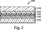
図2は、別の実例となる光学物品200の概略断面図である。光学物品200は、第1の剛性光学基材210と、第2の剛性光学基材220と、第1の剛性光学基材210と第2の剛性光学基材220との間に配置された自己支持性光学接着剤230と、を備える。自己支持性光学接着剤230は、上述のように、架橋シリコーン系ポリマーネットワークと、該ポリマーネットワーク内に少なくとも部分的に配置されたシリコーン流体と、を備える。
FIG. 2 is a schematic cross-sectional view of another illustrative
光学フィルム240(又は第3の剛性基材240)は、自己支持性光学接着剤230上に配置され、第2の光学接着剤250は、光学フィルム240上に配置されている。多くの実施形態では、第2の光学接着剤250は、硬化又は架橋し、光学フィルム240を第1の剛性光学基材210に永久的に固定する構造用接着剤である。他の実施形態では、第2の光学接着剤250は、自己支持性光学接着剤230が第2の剛性基材220に結合する力よりも大きな結合強度で、光学フィルム240を第1の剛性光学基材210に結合する、感圧性接着剤である。
The optical film 240 (or the third rigid substrate 240) is disposed on the self-supporting
多くの光学ディスプレイ用途では、第1の剛性光学基材210(例えば、タッチスクリーン又は他のセンサーパネル)又は保護カバーは、第2の剛性基材220(例えば、液晶ディスプレイパネル又はセル)から取り外し、第1の剛性光学基材210の交換品(例えば、タッチスクリーン又は他のセンサーパネル)又は保護カバーと交換することができる。
For many optical display applications, the first rigid optical substrate 210 (eg, touch screen or other sensor panel) or protective cover is removed from the second rigid substrate 220 (eg, liquid crystal display panel or cell); The first rigid
実例となる実施形態では、本明細書に記載の自己支持性接着剤は、例えば、LCDパネル及び該LCDを覆う透明センサー層、LCDパネル及び/又は該LCDを覆う保護カバー、又はLCDを覆う透明センサー層を備え、該透明センサーパネルを覆う保護カバーを備えるLCDパネルを備えることが可能なタブレットPCに利用される。タブレットPCは、一般的には、位置センサーと相互作用可能な能動的又は受動的なスタイラスとともに提供され、スタイラスは、LCDの上部又は下部に配置されてもよい。センサー要素がLCDの下部に配置される場合、透明保護カバーは、LCDを損傷から守るためにLCDの上部に提供され得る。次いで、センサー要素は透明LCDオーバーレイであり、透明センサー自体又は別個のカバー層によってLCDを保護することができる。本明細書に記載の自己支持性接着剤は、これらの剛性光学基材のいずれかの間に配置することができ、所望な場合、透明センサーパネル及び/又は保護カバーを比較的容易に除去することができる。例えば、オーバーレイセンサーパネルがうまく働かないか、又はセンサーオーバーレイ又は保護カバーに過度に引っかき傷ができたり、又は損傷した場合、本明細書に記載の自己支持性接着剤が、接着した剛性光学素子の永久的な再配置能を有するため、センサーパネル又は保護カバーは、簡単に交換することができる。 In illustrative embodiments, the self-supporting adhesive described herein can be, for example, an LCD panel and a transparent sensor layer that covers the LCD, an LCD panel and / or a protective cover that covers the LCD, or a transparent that covers the LCD. The tablet PC includes a sensor layer and can include an LCD panel including a protective cover that covers the transparent sensor panel. Tablet PCs are typically provided with an active or passive stylus that can interact with a position sensor, and the stylus may be placed on the top or bottom of the LCD. If the sensor element is located at the bottom of the LCD, a transparent protective cover can be provided on the top of the LCD to protect the LCD from damage. The sensor element is then a transparent LCD overlay, and the LCD can be protected by the transparent sensor itself or a separate cover layer. The self-supporting adhesive described herein can be placed between any of these rigid optical substrates and removes the transparent sensor panel and / or protective cover relatively easily if desired. be able to. For example, if the overlay sensor panel does not work well, or the sensor overlay or protective cover can be excessively scratched or damaged, the self-supporting adhesive described herein can be Due to its permanent relocation capability, the sensor panel or protective cover can be easily replaced.
多くの実施形態では、本明細書に記載の光学物品は、15%以下、10%以下、5%以下、3%以下、又は1%以下、又は0〜1%のヘイズ値を有することができる。多くの実施形態では、本明細書に記載の光学物品は、70%以上、80%以上、90%以上、又は95%以上の範囲の可視光透過率を有することができる。ヘイズ値及び可視光透過率値は、以下の試験法の項に定義されるように測定することができる。 In many embodiments, the optical articles described herein can have a haze value of 15% or less, 10% or less, 5% or less, 3% or less, or 1% or less, or 0 to 1%. . In many embodiments, the optical articles described herein can have a visible light transmission in the range of 70% or higher, 80% or higher, 90% or higher, or 95% or higher. The haze value and visible light transmittance value can be measured as defined in the Test Methods section below.
光学フィルムは、上述の光学特性を有する任意の材料であってよい。いくつかの実施形態では、光学基材は、任意の高分子材料であってよい。これらポリマー類の一部のリストとしては、例えば、ポリオレフィン類、ポリアクリレート類、ポリエステル類、ポリカーボネート類、フルオロポリマー類などが挙げられる。1つ以上のポリマー類を組み合わせて高分子光学フィルムを形成することができる。 The optical film may be any material having the optical properties described above. In some embodiments, the optical substrate can be any polymeric material. Some lists of these polymers include, for example, polyolefins, polyacrylates, polyesters, polycarbonates, fluoropolymers, and the like. One or more polymers can be combined to form a polymeric optical film.
いくつかの実施形態では、本明細書に記載の自己支持性接着剤は、平滑面を有する少なくとも1つの大きな表面を有することができる。他の実施形態では、接着剤は、構造化されたトポグラフィーを有する少なくとも1つの大きな表面を有する層であり得る。接着層表面の微細構造は、積層プロセス又は自己積層プロセス中に自己支持性接着剤と剛性基材との境界面で閉じ込められた空気又は他の流体が放出可能な特定の形状を有し得る。 In some embodiments, the self-supporting adhesive described herein can have at least one large surface with a smooth surface. In other embodiments, the adhesive can be a layer having at least one large surface with a structured topography. The microstructure of the adhesive layer surface may have a specific shape that allows air or other fluids entrapped at the interface between the self-supporting adhesive and the rigid substrate during the lamination or self-laminating process.
接着層の上の微細構造(及び、剥離ライナー上の対応する微細構造)は、少なくとも二方向で微視的であってもよい。微視的という用語は、本明細書で使用する時、顕微鏡の力を借りなければ、人間の目によっては解明するのが困難である寸法を指す。微視的の1つの有用な定義は、視力が定義され、認識可能な最も小さな文字の角サイズの観点で測定される。正常の視力では網膜上のアークの5分の高低角である輪郭を示す文字を検出できる。 The microstructure on the adhesive layer (and the corresponding microstructure on the release liner) may be microscopic in at least two directions. The term microscopic, as used herein, refers to a dimension that is difficult to elucidate by the human eye without the help of a microscope. One useful definition of microscopic is that visual acuity is defined and measured in terms of the smallest character corner size that can be recognized. With normal visual acuity, it is possible to detect a character indicating a contour that is 5 minutes high and low of the arc on the retina.
自己支持性接着層の微細構造は、米国特許第5,268,228号、同6,197,397号及び同6,123,890号(これらはそれぞれ参照することにより本明細書に組み込まれる)に記載されているように作ることが可能である。該トポグラフィーは、いずれかの接触技術、例えばキャスティング、コーティング、エンボス加工、又は圧縮によって接着層内に作製してよい。トポグラフィーは、(1)エンボスパターンを有するツール上に接着層をキャスティングする方法、(2)エンボスパターンを有する剥離ライナー上に接着層をコーティングする方法、又は、(3)接着層をニップロールに通して、エンボスパターンを有する剥離ライナーに対して接着剤を圧縮させる方法のうちの少なくとも1つによって作製してよい。エンボスパターンを作製する目的で用いるツールのトポグラフィーは、いずれかの既知の技術、例えば、化学エッチング、機械エッチング、レーザー切断、フォトリソグラフィー、ステレオリソグラフィー、マイクロマシニング、ナーリング、カッティング、又は、スコアリングを用いて作製してよい。 The microstructure of the self-supporting adhesive layer is described in U.S. Patent Nos. 5,268,228, 6,197,397 and 6,123,890, each of which is incorporated herein by reference. Can be made as described in The topography may be made in the adhesive layer by any contact technique, such as casting, coating, embossing, or compression. Topography consists of (1) a method of casting an adhesive layer on a tool having an embossed pattern, (2) a method of coating an adhesive layer on a release liner having an embossed pattern, or (3) passing the adhesive layer through a nip roll. And may be made by at least one of the methods of compressing the adhesive against a release liner having an embossed pattern. The topography of the tool used to create the embossed pattern can be any known technique, such as chemical etching, mechanical etching, laser cutting, photolithography, stereolithography, micromachining, knurling, cutting, or scoring. May be used.
ライナーは、自己支持性接着層又は微細構造化された接着層の上に配置することができるとともに、当業者に知られている任意の剥離ライナー又は転写ライナー(一部のケースでは、上記のようにエンボス加工ができるもの)にしてよい。該ライナーは、接着剤と緊密に接触させて配置してから、接着層を損傷させることなく取り外せるようにすることができる。ライナーの非限定的な例としては、ミネソタ州セントポールの3M社(3M Company)、イリノイ州ウィロウブルックのロパレックス(Loparex)、P.Sサブストレーツ社(P.S Substrates, Inc.)、ショーラーテクニカルペーパーズ社(Schoeller Technical Papers, Inc.)、アシドマンインコート社(AssiDoman Inncoat GMBH)、及び、P.W.A.クンスタッフ社(P.W.A. Kunstoff GMBH)から入手できる物質が挙げられる。ライナーは、剥離コーティングを有するポリマー被覆紙、剥離コーティングを有するポリエチレン被覆ポリエチレンテレフタレート(PET)フィルム、又は、剥離コーティングを有するキャストポリオレフィンフィルムにすることができる。接着層及び/又は剥離ライナーには、適宜に追加の非粘着性微細構造、例えば、米国特許第5,296,277号、同5,362,516号及び同5,141,790号に記載されているようなものが含まれてよい。非粘着性微細構造化を有する微細構造接着層は、ミネソタ州セントポール(St. Paul)の3M社(3M Company)から商品名コントロールタックプラス(CONTROLTAC PLUS)(商標)で入手可能である。 The liner can be placed over a self-supporting adhesive layer or a microstructured adhesive layer and can be any release liner or transfer liner known to those skilled in the art (as described above in some cases). Can be embossed). The liner can be placed in intimate contact with the adhesive and then removed without damaging the adhesive layer. Non-limiting examples of liners include 3M Company, St. Paul, Minnesota, Loparex, Willowbrook, Ill. S. Substrates, Inc., Schoeller Technical Papers, Inc., AssiDoman Inncoat GMBH, and P. S Substrates, Inc. W. A. Substances available from P.W.A. Kunstoff GMBH. The liner can be a polymer-coated paper with a release coating, a polyethylene-coated polyethylene terephthalate (PET) film with a release coating, or a cast polyolefin film with a release coating. Adhesive layers and / or release liners are optionally described in additional non-tacky microstructures, eg, US Pat. Nos. 5,296,277, 5,362,516 and 5,141,790. Something like that may be included. A microstructured adhesive layer having a non-tacky microstructure is available from 3M Company of St. Paul, Minnesota under the trade name CONTROLTAC PLUS ™.
該微細構造によって、規則的又は不規則なアレイ又はパターンを形成させることが可能である。規則的なアレイ又はパターンとしては例えば、直線的パターン、極性パターン、クロスハッチパターン、キューブコーナーパターンが挙げられる。該パターンは、キャリアウェブの方向と揃えてもよく、あるいは、キャリアウェブに対して斜めに整列させてもよい。微細構造のパターンは、適宜に接着層の主要面と反対面の双方の上に存在してもよい。これによって、該2つの面の各々の空気排出と接触表面積の個別制御を行って、2つの異なる境界面に対する接着特性が調整可能になる。 The microstructure can form a regular or irregular array or pattern. Examples of the regular array or pattern include a linear pattern, a polar pattern, a cross hatch pattern, and a cube corner pattern. The pattern may be aligned with the direction of the carrier web or may be aligned obliquely with respect to the carrier web. The microstructure pattern may optionally be present on both the major and opposite surfaces of the adhesive layer. This allows individual control of the air discharge and contact surface area of each of the two surfaces to adjust the adhesive properties for two different interface surfaces.
微細構造のパターンは、露出面から接着層の中まで伸びている実質的に連続的な開放経路又は溝を画定することができる。該経路は、自己支持性接着層の周縁部を終点とするか、物品の周縁部を終点とするその他の経路と連結するかのいずれかである。微細構造化された自己支持性接着層が剛性光学基材に適用される場合、該経路によって、自己支持性接着層と剛性光学基材との境界面に閉じ込められた流体が放出可能である。 The microstructure pattern can define a substantially continuous open path or groove extending from the exposed surface into the adhesive layer. The path is either the end point of the peripheral edge of the self-supporting adhesive layer or is connected to another path whose end point is the peripheral edge of the article. When a microstructured self-supporting adhesive layer is applied to a rigid optical substrate, the pathway can release fluid confined at the interface between the self-supporting adhesive layer and the rigid optical substrate.
接着層内の微細構造の形状は、特定の用途で求められる流体放出及び剥離接着のレベルとともに、基材の表面特性と同様、大きく変わり得る。突出部と凹部を用いてよく、微細構造は、接着層に溝が形成できるように連続的であることが可能である。好適な形状としては、パターン密度、接着性能、及び微細構造を製造するための方法が容易に利用可能であるという理由のため、半球、正角錐、三角錐、正四角錐、四角錐及び「V字型」の溝が挙げられる。微細構造は、体系的に又は不規則に生成させてよい。 The shape of the microstructure within the adhesive layer can vary greatly, as well as the surface properties of the substrate, with the level of fluid release and peel adhesion required for a particular application. Protrusions and recesses may be used, and the microstructure can be continuous so that grooves can be formed in the adhesive layer. Suitable shapes include hemisphere, regular pyramid, triangular pyramid, regular quadrangular pyramid, quadrangular pyramid and “V-shape” because pattern density, adhesion performance, and methods for producing microstructures are readily available. Type "groove. The microstructure may be generated systematically or irregularly.
本発明は、上に記載した特定の実施例に限られるとみなすべきではなく、添付の請求項で明確に提示されているとおり、本発明のあらゆる態様を網羅していると理解すべきである。様々な修正、同等の方法、及び本発明を適用可能である多くの構造は、本発明が対象とする技術分野の当業者が本発明の明細書を検討することにより、容易に明らかになるであろう。 The present invention should not be considered limited to the particular embodiments described above, but should be understood to cover all aspects of the present invention as clearly set forth in the appended claims. . Various modifications, equivalent methods, and many structures to which the present invention can be applied will be readily apparent to those skilled in the art to which the present invention is directed by studying the specification of the invention. I will.
これらの実施例は単にあくまで例示を目的としたものであり、添付の請求項の範囲を制限することを意味するものではない。特に記載のない限り、実施例及びこれ以降の明細書に記載される部、百分率、比率等は全て、重量による。使用される溶媒及びその他の試薬は、特に記載のない限り、シグマ・アルドリッチ・ケミカル社(Sigma-Aldrich Chemical Company)(ウィスコンシン州ミルウォーキー(Milwaukee))より入手した。 These examples are for illustrative purposes only and are not meant to limit the scope of the appended claims. Unless stated otherwise, all parts, percentages, ratios, etc. described in the examples and the following specification are by weight. Solvents and other reagents used were obtained from Sigma-Aldrich Chemical Company (Milwaukee, Wis.) Unless otherwise noted.

試験方法
視感透過率(可視光透過率)、ヘイズ及び透明性
全試料の視感透過率及びヘイズは、米国試験測定協会(American Society for Testing and Measurement)(ASTM)試験法D 1003−95(「透明なプラスチックのヘイズ及び視感透過率のための標準試験(Standard Test for Haze and Luminous Transmittance of Transparent Plastic)」)に従い、ミッドランド州シルバー・スプリングス(Silver Springs)のBYK−ガードナー社(BYK-Gardner Inc.)製のTCS・プラス・分光分析装置(TCS Plus Spectrophotometer)を用いて測定した。試料の透過率スペクトル及び反射率スペクトルは、パーキン−エルマー・ラムダ9分光分析装置(Perkin-Elmer Lambda 9 spectrophotometer)を用いて測定した。PET(50マイクロメートル)とガラスとの間に接着試料をはさんで調製した積層体で試験した。同じ装置及び積層体を使用して透明性も測定した。
Test Method Luminous Transmittance (Visible Light Transmittance), Haze and Transparency The luminous transmittance and haze of all samples were measured by American Society for Testing and Measurement (ASTM) test method D 1003-95 ( BYK-Gardner (Silver Springs, Midland) according to "Standard Test for Haze and Luminous Transmittance of Transparent Plastic" Inc.) was measured using a TCS Plus Spectrophotometer. The transmittance spectrum and reflectance spectrum of the sample were measured using a Perkin-Elmer Lambda 9 spectrophotometer. A laminate prepared by sandwiching an adhesive sample between PET (50 micrometers) and glass was tested. Transparency was also measured using the same equipment and laminate.
180°剥離接着性
この剥離接着試験は、ASTM D 3330−90に記載の試験法と同様であり、ガラス基材を該試験に記載のステンレス鋼基材の代用とする。
180 ° Peel Adhesion This peel adhesion test is similar to the test method described in ASTM D 3330-90, and a glass substrate is substituted for the stainless steel substrate described in the test.
ポリエステルフィルム上の接着性コーティング材を、1.27センチメートルX15センチメートルの切れ端へと切断した。次に、ストリップの上を2キログラムのローラーを一度通過させ、各ストリップを10センチメートル×20センチメートルの清潔な溶媒洗浄されたガラス製試験片に付着させた。該結合品を室温で1週間又は70℃で1週間放置した。IMASS滑り/剥離試験機(3M90型、オハイオ州ストロングスビル(Strongsville)のインスツルメンターズ社(Instrumentors Inc.)から入手)を用い、速度2.3メートル/分(90インチ/分)、データ収集時間5秒間で180°剥離接着性について試料を試験した。2つの試料を試験した。報告された剥離接着値は、2つの試料の各々からの剥離接着値の平均値である。グラム/インチ(g/in)の単位でデータを収集し、ニュートン/デシメートル(N/dm)に変換した。 The adhesive coating material on the polyester film was cut into pieces of 1.27 centimeters by 15 centimeters. The strip was then passed once through a 2 kilogram roller and each strip was adhered to a 10 cm x 20 cm clean solvent-washed glass specimen. The bound product was left at room temperature for 1 week or at 70 ° C. for 1 week. Data acquisition using IMASS slip / peel tester (model 3M90, obtained from Instrumentors Inc., Strongsville, Ohio), speed 2.3 meters / minute (90 inches / minute) Samples were tested for 180 ° peel adhesion over a period of 5 seconds. Two samples were tested. The reported peel adhesion value is the average of the peel adhesion values from each of the two samples. Data was collected in units of grams / inch (g / in) and converted to Newton / decimeter (N / dm).
濡れ試験の速度
下塗りされたPETにコーティングされた試料をガラス基材に積層し、濡れ速度を観察し、濡れ速度を1〜5のランクに分けることによって積層容易性を試験した。スケール「1」は最も濡れ速度が小さく、「5」は最も濡れ速度が大きい。
Wetting Test Speed A sample coated with primed PET was laminated to a glass substrate, the wetting speed was observed, and the ease of lamination was tested by dividing the wetting speed into 1-5 ranks. Scale “1” has the lowest wetting rate, and “5” has the highest wetting rate.
剛性体と剛性体との積層の浸潤試験
下塗りされたPET上に接着剤をコーティングした試料を、複数層の積層体におけるガラスとガラスとの積層について試験した。下塗りされていないPETライナー/実施例の接着剤/下塗りされたPETの試料構造物の下塗りされたPETの側に、光学的に透明な二重ライナー粘着転写剤(ミネソタ州セントポール(St. Paul)の3M社(3M Company)から市販されている3M光学透明積層接着剤(Optically Clear Laminating Adhesive)8141)を積層し、粘着転写ライナー/粘着転写剤/下塗りされたPET/実施例の接着剤/下塗りされていないPETライナーの構造物を作成した。粘着転写ライナーを外し、構造物をガラススライドの5.0センチメートル×7.6センチメートル(2インチ×3インチ)の領域に、厚さ1mmで積層させた。下塗りされていないPETライナーを外し、実施例の接着剤をガラス片の15センチメートル×20センチメートル(6インチ×8インチ)の領域に、厚さ1mmで置いた。構造物を指で押さえたり、ローラーで積層させたりはしなかった。実施例の接着剤は、重力によって浸潤し、自動的に積層した。開始すると同時に浸潤した場合、その試料に、剛性体と剛性体との積層の浸潤について、「はい」の評価をした。1分以内に浸潤が始まらない場合、ガラススライドの一端を指で押し、浸潤前線を開始させようと試みた。浸潤が開始した場合、その試料に、剛性体と剛性体との積層の浸潤について、「はい」の評価をした。ガラススライドの端を指で押した後でも、5分後に浸潤がほとんど起こらないか、全く起こらない場合、その試料に、剛性体と剛性体との積層の浸潤について、「いいえ」の評価をした。浸潤は開始するが、汚れ粒子、コーティングの厚さ変位又は他の異常によって浸潤の中断が観察された場合、その試料に、剛性体と剛性体との積層の浸潤について、「はい」の評価をした。
Infiltration test of laminate of rigid body and rigid body Samples coated with adhesive on primed PET were tested for glass-to-glass lamination in a multi-layer laminate. An uncoated PET liner / example adhesive / primed PET sample structure on the side of the primed PET with an optically clear double liner adhesive transfer agent (St. Paul, MN) 3M Optical Clear Laminating Adhesive 8141) commercially available from 3M Company, adhesive transfer liner / adhesive transfer agent / primed PET / example adhesive / An unprimed PET liner structure was created. The adhesive transfer liner was removed and the structure was laminated to a 5.0 centimeter x 7.6 centimeter (2 inch x 3 inch) area of the glass slide with a thickness of 1 mm. The unprimed PET liner was removed and the example adhesive was placed on a 15 cm × 20 cm (6 inch × 8 inch) area of a piece of glass with a thickness of 1 mm. The structure was not pressed with fingers or laminated with rollers. The adhesives of the examples infiltrated by gravity and laminated automatically. When the sample infiltrated at the same time as the start, the sample was evaluated as “Yes” for the infiltration of the laminate of the rigid body and the rigid body. If infiltration did not begin within 1 minute, one end of the glass slide was pushed with a finger to attempt to initiate the infiltration front. When the infiltration started, the sample was evaluated as “Yes” for the infiltration of the laminate of the rigid body and the rigid body. Even if the edge of the glass slide was pushed with a finger, if the infiltration hardly occurred or not at all after 5 minutes, the sample was evaluated as “No” for the infiltration of the laminate of the rigid body and the rigid body. . Infiltration begins, but if disruption of the infiltration is observed due to dirt particles, coating thickness displacement or other anomalies, the sample should be rated “Yes” for the infiltration of the laminate of rigid bodies. did.
調製例1:シリコーンポリ尿素(SPU)エラストマーの合成
反応槽に、十分な量の2−プロパノール中のPDMSジアミン33,000、DYTEK A、H12MDIをモル比1:1:2で入れ、固形分20%の溶液を得た。混合物を2時間攪拌し、シリコーンポリ尿素エラストマーを得た。
Preparation Example 1: Synthesis of Silicone Polyurea (SPU) Elastomer A sufficient amount of PDMS diamine 33,000, DYTEK A, H12MDI in 2-propanol in a molar ratio of 1: 1: 2 was placed in a reaction vessel with a solid content of 20 % Solution was obtained. The mixture was stirred for 2 hours to obtain a silicone polyurea elastomer.
調製例2:シリコーンポリオキサミドエラストマー前駆体の合成
シュウ酸ジエチル(241.10グラム)を、機械式撹拌機、加熱マントル、窒素導入用チューブ(ストップコック付き)、及び排出管を装備した3リットルの3つ口樹脂フラスコ内に入れた。フラスコを窒素で15分間パージし、次に、撹拌しながら、PDMSジアミン5,000(2,028.40グラム、分子量が4,918グラム/モルに相当する)をゆっくりと加えた。室温にて8時間後、反応フラスコに、蒸留アダプタ及び蒸留レシーバを装着した。該内容物を攪拌し、減圧下(133パスカル、(1トール))にて150℃まで4時間、更なる留出物を集めることができなくなるまで加熱した。残った液体を室温まで冷却し、2,573グラムを得た。透明で流動性の液体のガスクロマトグラフィー分析は、検出可能濃度のシュウ酸ジエチルが残存していないことを示した。分子量は、1H NMR(5,477グラム/モルに相当する分子量)を使用し、滴定(2個の滴定された試料について2,722グラム/当量及び2,721グラム/当量の当量)によって決定した。
Preparation Example 2: Synthesis of silicone polyoxamide elastomer precursor 3 liters of diethyl oxalate (241.10 grams) equipped with mechanical stirrer, heating mantle, nitrogen inlet tube (with stopcock), and discharge tube In a three-necked resin flask. The flask was purged with nitrogen for 15 minutes and then PDMS diamine 5,000 (2,028.40 grams, corresponding to a molecular weight of 4,918 grams / mole) was slowly added with stirring. After 8 hours at room temperature, the reaction flask was equipped with a distillation adapter and a distillation receiver. The contents were stirred and heated under reduced pressure (133 Pascal, (1 Torr)) to 150 ° C. for 4 hours until no further distillate could be collected. The remaining liquid was cooled to room temperature, yielding 2,573 grams. Gas chromatographic analysis of a clear, fluid liquid showed no detectable concentration of diethyl oxalate remaining. The molecular weight is determined by titration (equivalent of 2,722 grams / equivalent and 2,721 grams / equivalent for two titrated samples) using 1 H NMR (molecular weight equivalent to 5,477 grams / mole). did.
調製例3:シリコーンポリオキサミドHDAエラストマーの合成
調製例2の前駆体(793.20グラム)を、機械式撹拌機、加熱マントル、窒素導入用チューブ(ストップコック付き)及び排出管を装備した3リットルの3つ口樹脂フラスコ内に入れた。フラスコを窒素で15分間パージし、HDA(17.48グラム)を添加した。混合物を機械的に撹拌し、かつ150℃まで窒素雰囲気下で3.5時間加熱した。粘稠な溶融生成物をガラストレーに注ぎ、冷却し、固体生成物をTHFに溶解した(1,620グラム)。
Preparation Example 3: Synthesis of Silicone Polyoxamide HDA Elastomer The precursor of Preparation Example 2 (793.20 grams) was equipped with a mechanical stirrer, heating mantle, nitrogen introduction tube (with stopcock) and discharge tube 3 Placed in a liter three-necked resin flask. The flask was purged with nitrogen for 15 minutes and HDA (17.48 grams) was added. The mixture was mechanically stirred and heated to 150 ° C. under a nitrogen atmosphere for 3.5 hours. The viscous molten product was poured into a glass tray, cooled and the solid product was dissolved in THF (1,620 grams).
調製例4:シリコーンポリオキサミドEDAエラストマーの合成
調製例2の前駆体(100.00グラム)を広口瓶に入れた。EDA(1.0243グラム)を添加した。瓶を密閉し、内容物が粘稠過ぎて流れなくなるまで混合物を素早く撹拌した。一晩、周囲温度にて撹拌した後、固体生成物をTHF(200グラム)中に溶解させた。
Preparation Example 4: Synthesis of Silicone Polyoxamide EDA Elastomer The precursor of Preparation Example 2 (100.00 grams) was placed in a jar. EDA (1.0243 grams) was added. The bottle was sealed and the mixture was stirred rapidly until the contents were too viscous to flow. After stirring overnight at ambient temperature, the solid product was dissolved in THF (200 grams).
調製例5:シリコーンポリオキサミドXDAエラストマーの合成
調製例2の前駆体(100.00グラム)及びXDA(2.32グラム)を瓶に量り取った。瓶を密閉し、内容物が粘稠過ぎて流れなくなるまで混合物を素早く撹拌した。ローラーミル上に瓶を周囲温度にて一晩置いた。固体生成物をTHF(200グラム)中に溶解させた。
Preparation Example 5: Synthesis of Silicone Polyoxamide XDA Elastomer The precursor of Preparation Example 2 (100.00 grams) and XDA (2.32 grams) were weighed into a bottle. The bottle was sealed and the mixture was stirred rapidly until the contents were too viscous to flow. The bottle was placed on a roller mill overnight at ambient temperature. The solid product was dissolved in THF (200 grams).
実施例1〜3及び比較実施例C1
実施例1〜3の場合、上述のように調製したシリコーンポリ尿素エラストマーと、添加油及び架橋添加剤とを従来の溶媒媒体を用いて固形分20%でブレンドすることによって、シリコーンポリ尿素エラストマー接着剤を調製した。比較例C1では、添加油又は架橋添加剤を使用しなかった。溶媒混合物から、これらの試料を下塗りされたPET表面にコーティングし、厚さ25マイクロメートルになるまで乾燥させ、表1に記載されるように硬化させた。室温又は70℃で1週間エージングした後、上述の試験法に従って、180°剥離について試料を試験した。これらのデータを表2にまとめている。更に、上述の濡れ速度及び剛性体と剛性体との積層の浸潤試験を用いて試料を試験し、データを表2に示す。実施例2では、上述の試験法を用いて視感透過率、ヘイズ及び透明性を測定し、データを表6に示す。
Examples 1-3 and Comparative Example C1
In the case of Examples 1-3, silicone polyurea elastomer adhesion was achieved by blending the silicone polyurea elastomer prepared as described above with additive oil and crosslinking additive at 20% solids using a conventional solvent medium. An agent was prepared. In Comparative Example C1, no additive oil or crosslinking additive was used. From the solvent mixture, these samples were coated on the primed PET surface, dried to a thickness of 25 micrometers, and cured as described in Table 1. After aging for 1 week at room temperature or 70 ° C., the samples were tested for 180 ° peel according to the test method described above. These data are summarized in Table 2. Furthermore, the samples were tested using the above-described wetting rate and the infiltration test of the laminate of rigid and rigid bodies, and the data is shown in Table 2. In Example 2, the luminous transmittance, haze, and transparency were measured using the test method described above, and the data are shown in Table 6.
NT=試験せず
実施例4〜5及び比較例C2〜C3
実施例4〜5及び比較例C2〜C3の場合、表3に示す比率の33K MAUS、IOA及び添加油と、1重量%のダロキュア(DAROCUR)1173とをブレンドすることによってシリコーンアクリレート接着剤を調製した。これらの処方試料を、下塗りされたPETフィルムにコーティングし、下塗りされていないPETフィルム(剥離ライナーとして使用)で覆い、350nmの低密度UV光で15分間硬化させた。上述の試験法に記載されるように、濡れ速度及び剛性体と剛性体との積層の浸潤試験を用いて試料を試験した。データを表3にまとめている。
NT = not tested Examples 4-5 and Comparative Examples C2-C3
For Examples 4-5 and Comparative Examples C2-C3, silicone acrylate adhesives were prepared by blending the ratios of 33K MAUS, IOA and additive oils shown in Table 3 with 1 wt% DAROCUR 1173. did. These formulated samples were coated onto primed PET film, covered with unprimed PET film (used as a release liner), and cured with 350 nm low density UV light for 15 minutes. Samples were tested using the wetting rate and infiltration test of the laminate of rigid and rigid bodies as described in the test method above. The data is summarized in Table 3.
(実施例6〜8)
実施例6〜8の場合、上述の調製例に記載されるように調製したシリコーンポリオキサミドエラストマーと、添加油及び架橋添加剤とを従来の溶媒媒体を用いて固形分20%でブレンドすることによって、シリコーンポリオキサミドエラストマー接着剤を調製した。実施例6の場合、シリコーンポリオキサミドエラストマーは、調製例3で調製されたHDAエラストマーであり、実施例7の場合、シリコーンポリオキサミドエラストマーは、調製例4で調製されたEDAエラストマーであり、実施例8の場合、シリコーンポリオキサミドエラストマーは、調製例5で調製されたXDAエラストマーであった。溶媒混合物から、これらの試料を下塗りされたPET表面にコーティングし、厚さ25マイクロメートルメートルになるまで乾燥させ、表4に記載されるように硬化させた。室温又は70℃で3日間エージングした後、上述の試験法に従って、180°剥離について試料を試験した。これらのデータを表5にまとめている。更に、上述の濡れ速度試験を用いて試料を試験し、データを表5に示す。上述の試験法を用いて視感透過率、ヘイズ及び透明性を測定し、データを表6に示す。
(Examples 6 to 8)
For Examples 6-8, blend the silicone polyoxamide elastomer prepared as described in the Preparation Examples above with the additive oil and cross-linking additive at 20% solids using a conventional solvent medium. A silicone polyoxamide elastomer adhesive was prepared. In the case of Example 6, the silicone polyoxamide elastomer is the HDA elastomer prepared in Preparation Example 3, and in the case of Example 7, the silicone polyoxamide elastomer is the EDA elastomer prepared in Preparation Example 4. In the case of Example 8, the silicone polyoxamide elastomer was the XDA elastomer prepared in Preparation Example 5. From the solvent mixture, these samples were coated onto the primed PET surface, dried to a thickness of 25 micrometers and cured as described in Table 4. After aging at room temperature or 70 ° C. for 3 days, the samples were tested for 180 ° peel according to the test method described above. These data are summarized in Table 5. In addition, the samples were tested using the wetting rate test described above and the data is shown in Table 5. The luminous transmittance, haze, and transparency were measured using the test method described above, and the data are shown in Table 6.
(実施例9)
実施例9の場合、比較例C3と同じ処方を用い、表7に示す比率の33K MAUS、IOA及び添加油と、1重量%のダロキュア(DAROCUR)1173とをブレンドすることによってシリコーンアクリレート接着剤を調製した。この処方試料を、下塗りされたPETフィルムにコーティングし、下塗りされていないPETフィルム(剥離ライナーとして使用)で覆い、350nmの低密度UV光で15分間硬化させた。濡れ速度について試料を試験した。データを表7に示す。実施例の接着剤を積層させるガラスプレートを添加油の薄層で前処理するという、剛性体と剛性体との積層の浸潤試験の改良法を行った。薄層をふき取り、かみそりの刃で過剰の油を取り除くことによって添加油を適用し、均一な薄いコーティングを得た。データを表7にまとめている。
Example 9
In the case of Example 9, using the same formulation as Comparative Example C3, the silicone acrylate adhesive was blended by blending 33K MAUS, IOA and additive oil in the ratios shown in Table 7 with 1 wt% DAROCUR 1173. Prepared. The formulated sample was coated on a primed PET film, covered with an unprimed PET film (used as a release liner), and cured with 350 nm low density UV light for 15 minutes. Samples were tested for wetting rate. The data is shown in Table 7. The improvement method of the infiltration test of lamination | stacking of a rigid body that the glass plate which laminates | stacks the adhesive agent of an Example is pre-processed with the thin layer of an addition oil was performed. The additive oil was applied by wiping the thin layer and removing excess oil with a razor blade to obtain a uniform thin coating. The data is summarized in Table 7.
(態様1)(Aspect 1)
第1の剛性光学基材と、A first rigid optical substrate;
第2の剛性光学基材と、A second rigid optical substrate;
前記第1の剛性光学基材と前記第2の剛性光学基材との間に配置された自己支持性光学接着剤であって前記自己支持性光学接着剤は、架橋シリコーン系ポリマーネットワーク、及び前記ポリマーネットワークに配置されたシリコーン流体を含む、接着剤と、A self-supporting optical adhesive disposed between the first rigid optical substrate and the second rigid optical substrate, the self-supporting optical adhesive comprising a crosslinked silicone polymer network; and An adhesive comprising a silicone fluid disposed in a polymer network;
を含む、光学物品。An optical article comprising:
(態様2)(Aspect 2)
前記架橋シリコーン系ポリマーネットワークが、シリコーンポリ尿素エラストマーを含む、態様1に記載の光学物品。The optical article according to aspect 1, wherein the crosslinked silicone-based polymer network comprises a silicone polyurea elastomer.
(態様3)(Aspect 3)
前記架橋シリコーン系ポリマーネットワークが、シリコーンポリアクリレートを含む、態様1に記載の光学物品。The optical article according to aspect 1, wherein the crosslinked silicone-based polymer network comprises a silicone polyacrylate.
(態様4)(Aspect 4)
前記架橋シリコーン系ポリマーネットワークが、シリコーンポリオキサミドエラストマーを含む、態様1に記載の光学物品。The optical article according to aspect 1, wherein the crosslinked silicone-based polymer network includes a silicone polyoxamide elastomer.
(態様5)(Aspect 5)
前記自己支持性光学接着剤が、20〜50重量%のシリコーン流体を含む、態様1に記載の光学物品。The optical article of aspect 1, wherein the self-supporting optical adhesive comprises 20 to 50 wt% silicone fluid.
(態様6)(Aspect 6)
前記自己支持性光学接着剤が、50〜80重量%のシリコーンエラストマーを含む、態様1に記載の光学物品。The optical article according to aspect 1, wherein the self-supporting optical adhesive comprises 50-80 wt% silicone elastomer.
(態様7)(Aspect 7)
前記第1の剛性光学基材及び前記第2の剛性光学基材が、ガラス又は石英を含む、態様1に記載の光学物品。The optical article according to aspect 1, wherein the first rigid optical substrate and the second rigid optical substrate include glass or quartz.
(態様8)(Aspect 8)
前記光学物品が、ASTM試験法D 1003−95に従って測定した場合、5%未満のヘイズ値を有し、90%以上の可視光透過率を有する、態様1に記載の光学物品。The optical article according to aspect 1, wherein the optical article has a haze value of less than 5% and a visible light transmittance of 90% or more when measured according to ASTM test method D 1003-95.
(態様9)(Aspect 9)
前記自己支持性光学接着剤が、光学フィルムの第1面に配置されており、第2の光学接着剤が、前記光学フィルムの第2面に配置されており、前記第2面が、前記光学フィルムの第1面の反対側にある、態様1に記載の光学物品。The self-supporting optical adhesive is disposed on the first surface of the optical film, the second optical adhesive is disposed on the second surface of the optical film, and the second surface is the optical surface. The optical article according to aspect 1, wherein the optical article is on the opposite side of the first side of the film.
(態様10)(Aspect 10)
前記自己支持性光学接着剤が、永久的に再配置可能な光学接着剤であり、前記第2の光学接着剤が構造用接着剤である、態様9に記載の光学物品。The optical article according to aspect 9, wherein the self-supporting optical adhesive is a permanently repositionable optical adhesive and the second optical adhesive is a structural adhesive.
(態様11)(Aspect 11)
前記第2の剛性光学基材が、液晶ディスプレイパネルの少なくとも一部分を形成する、態様1に記載の光学物品。The optical article of aspect 1, wherein the second rigid optical substrate forms at least a portion of a liquid crystal display panel.
(態様12)(Aspect 12)
前記第1の剛性光学基材が、透明センサーパネルの少なくとも一部分を形成する、態様1に記載の光学物品。The optical article of aspect 1, wherein the first rigid optical substrate forms at least a portion of a transparent sensor panel.
(態様13)(Aspect 13)
前記第1の剛性光学基材が、透明センサーパネルの少なくとも一部分を形成し、前記第2の剛性光学基材が、液晶ディスプレイパネルの少なくとも一部分を形成する、態様1に記載の光学物品。The optical article according to aspect 1, wherein the first rigid optical substrate forms at least a portion of a transparent sensor panel and the second rigid optical substrate forms at least a portion of a liquid crystal display panel.
(態様14)(Aspect 14)
表面を有する第1の剛性光学基材、及び前記表面に隣接して配置された自己支持性光学接着剤を提供する工程であって、前記自己支持性光学接着剤は、架橋シリコーン系ポリマーネットワーク、及び前記ポリマーネットワークに配置されたシリコーン流体を含む、工程と、Providing a first rigid optical substrate having a surface and a self-supporting optical adhesive disposed adjacent to the surface, the self-supporting optical adhesive comprising a crosslinked silicone polymer network, And including a silicone fluid disposed in the polymer network;
前記自己支持性光学接着層の上に第2の剛性基材を積層して、光学物品を形成する工程であって、前記自己支持性光学接着層は、第1の剛性光学基材と第2の光学基材との間に配置される、工程と、Laminating a second rigid substrate on the self-supporting optical adhesive layer to form an optical article, the self-supporting optical adhesive layer comprising a first rigid optical substrate and a second rigid optical substrate. A step disposed between the optical substrate and
を含む、光学物品を形成する方法。A method of forming an optical article, comprising:
(態様15)(Aspect 15)
前記提供する工程が、前記自己支持性光学接着層の上に配置された光学フィルム、及び前記光学フィルムの反対側の表面に配置された第2の光学接着層を更に備え、前記第2の光学接着剤が、前記光学フィルムと前記第1の剛性基材との間に配置されている、態様14に記載の方法。The providing step further comprises: an optical film disposed on the self-supporting optical adhesive layer; and a second optical adhesive layer disposed on the opposite surface of the optical film, wherein the second optical The method according to aspect 14, wherein an adhesive is disposed between the optical film and the first rigid substrate.
(態様16)(Aspect 16)
前記積層する工程が、液晶ディスプレイパネルを備える第2の剛性基材を前記自己支持性光学接着層の上に積層し、光学物品を形成する工程を含む、態様14に記載の方法。The method of aspect 14, wherein the laminating step comprises laminating a second rigid substrate comprising a liquid crystal display panel on the self-supporting optical adhesive layer to form an optical article.
(態様17)(Aspect 17)
前記提供する工程が、透明センサーパネルを含む第1の剛性光学基材を提供する工程を含む、態様14に記載の方法。15. The method of aspect 14, wherein the providing step comprises providing a first rigid optical substrate that includes a transparent sensor panel.
(態様18)(Aspect 18)
前記第2の剛性基材から、前記第1の剛性基材及び前記自己支持性光学接着層を剥離する工程を更に含む、態様14に記載の方法。The method according to aspect 14, further comprising the step of peeling the first rigid substrate and the self-supporting optical adhesive layer from the second rigid substrate.
(態様19)(Aspect 19)
表面を有する第1の剛性光学基材の交換品、及び前記表面に隣接して配置された自己支持性光学接着剤を提供する工程であって、前記自己支持性光学接着剤は、架橋シリコーン系ポリマーネットワーク、及び前記ポリマーネットワークに配置されたシリコーン流体を含む、工程と、Providing a replacement for a first rigid optical substrate having a surface, and a self-supporting optical adhesive disposed adjacent to the surface, the self-supporting optical adhesive comprising a crosslinked silicone system Comprising a polymer network and a silicone fluid disposed in the polymer network;
前記第2の剛性基材を前記第1の剛性光学基材の自己支持性光学接着層の交換品の上に積層して、修理された光学物品を形成する工程と、を更に含み、Laminating the second rigid substrate on a replacement for the self-supporting optical adhesive layer of the first rigid optical substrate to form a repaired optical article;
前記第1の剛性光学基材の自己支持性光学接着層の交換品が、前記第1の剛性光学基材の交換品と前記第2の光学基材との間に配置されている、態様18に記載の方法。Aspect 18 in which the replacement of the self-supporting optical adhesive layer of the first rigid optical substrate is disposed between the replacement of the first rigid optical substrate and the second optical substrate. The method described in 1.
(態様20)(Aspect 20)
前記提供する工程が、微細構造化された接着剤表面を有する自己支持性光学接着層を提供する工程を更に含む、態様14に記載の方法。15. The method of aspect 14, wherein the providing step further comprises providing a self-supporting optical adhesive layer having a microstructured adhesive surface.
Claims (3)
第2の剛性光学基材と、
前記第1の剛性光学基材と前記第2の剛性光学基材との間に配置された自己支持性光学接着剤とを含む光学物品であって、
前記自己支持性光学接着剤は、架橋シリコーン系ポリマーネットワーク、及び前記ポリマーネットワークに配置されたシリコーン流体を含むことを特徴とする、光学物品。A first rigid optical substrate;
A second rigid optical substrate;
An optical article comprising a self-supporting optical adhesive disposed between the first rigid optical substrate and the second rigid optical substrate ,
The self-supporting optical adhesive characterized by containing crosslinked silicone polymer networks, and the placed silicone fluid to the polymer network, optical article.
Applications Claiming Priority (3)
| Application Number | Priority Date | Filing Date | Title |
|---|---|---|---|
| US11/426,844 US7655283B2 (en) | 2006-06-27 | 2006-06-27 | Rigid optical laminates and methods of forming the same |
| US11/426,844 | 2006-06-27 | ||
| PCT/US2007/071160 WO2008002772A1 (en) | 2006-06-27 | 2007-06-14 | Rigid optical laminates and methods of forming the same |
Publications (3)
| Publication Number | Publication Date |
|---|---|
| JP2009543132A JP2009543132A (en) | 2009-12-03 |
| JP2009543132A5 JP2009543132A5 (en) | 2010-07-29 |
| JP5180204B2 true JP5180204B2 (en) | 2013-04-10 |
Family
ID=38845960
Family Applications (1)
| Application Number | Title | Priority Date | Filing Date |
|---|---|---|---|
| JP2009518439A Expired - Fee Related JP5180204B2 (en) | 2006-06-27 | 2007-06-14 | Rigid optical laminate and method for forming the same |
Country Status (6)
| Country | Link |
|---|---|
| US (1) | US7655283B2 (en) |
| EP (1) | EP2035225B1 (en) |
| JP (1) | JP5180204B2 (en) |
| KR (1) | KR101323499B1 (en) |
| CN (1) | CN101479104B (en) |
| WO (1) | WO2008002772A1 (en) |
Families Citing this family (42)
| Publication number | Priority date | Publication date | Assignee | Title |
|---|---|---|---|---|
| US8936057B2 (en) * | 2005-08-30 | 2015-01-20 | Rockwell Collins, Inc. | Substrate lamination system and method |
| US8603288B2 (en) | 2008-01-18 | 2013-12-10 | Rockwell Collins, Inc. | Planarization treatment of pressure sensitive adhesive for rigid-to-rigid substrate lamination |
| US8118075B2 (en) * | 2008-01-18 | 2012-02-21 | Rockwell Collins, Inc. | System and method for disassembling laminated substrates |
| US8137498B2 (en) | 2005-08-30 | 2012-03-20 | Rockwell Collins Inc. | System and method for completing lamination of rigid-to-rigid substrates by the controlled application of pressure |
| US8691043B2 (en) * | 2005-08-30 | 2014-04-08 | Rockwell Collins, Inc. | Substrate lamination system and method |
| US20080318065A1 (en) * | 2007-06-22 | 2008-12-25 | Sherman Audrey A | Mixtures of polydiorganosiloxane polyamide-containing components and organic polymers |
| US9733349B1 (en) | 2007-09-06 | 2017-08-15 | Rockwell Collins, Inc. | System for and method of radar data processing for low visibility landing applications |
| US9939526B2 (en) | 2007-09-06 | 2018-04-10 | Rockwell Collins, Inc. | Display system and method using weather radar sensing |
| KR20100103870A (en) | 2008-01-11 | 2010-09-28 | 쓰리엠 이노베이티브 프로퍼티즈 컴파니 | Stretch releasing optically clear pressure sensitive adhesive |
| EP3135490B1 (en) | 2008-01-18 | 2018-08-22 | Rockwell Collins, Inc. | Substrate lamination apparatus |
| JP2009221380A (en) * | 2008-03-17 | 2009-10-01 | Lintec Corp | Adhesive sheet and separate sheet-attached adhesive sheet using the same |
| US8431671B2 (en) * | 2008-03-26 | 2013-04-30 | 3M Innovative Properties Company | Structured polydiorganosiloxane polyamide containing devices and methods |
| KR20110104034A (en) | 2008-12-17 | 2011-09-21 | 쓰리엠 이노베이티브 프로퍼티즈 캄파니 | Thermoplastic silicone-based polymer process additives for injection molding applications |
| ES2603214T3 (en) * | 2008-12-17 | 2017-02-24 | 3M Innovative Properties Company | Silicone-polyoxamide processing additives for high transparency applications |
| JP5869494B2 (en) | 2009-12-08 | 2016-02-24 | スリーエム イノベイティブ プロパティズ カンパニー | Optical structure incorporating light guide and low refractive index film |
| US8486535B1 (en) | 2010-05-24 | 2013-07-16 | Rockwell Collins, Inc. | Systems and methods for adherable and removable thin flexible glass |
| US8576370B1 (en) | 2010-06-30 | 2013-11-05 | Rockwell Collins, Inc. | Systems and methods for nonplanar laminated assemblies |
| US8643260B1 (en) | 2011-09-02 | 2014-02-04 | Rockwell Collins, Inc. | Systems and methods for display assemblies having printed masking |
| KR20130046758A (en) * | 2011-10-28 | 2013-05-08 | 삼성디스플레이 주식회사 | Windowfor display protection and display using the same |
| US8647727B1 (en) | 2012-06-29 | 2014-02-11 | Rockwell Colllins, Inc. | Optical assembly with adhesive layers configured for diffusion |
| WO2014018231A1 (en) * | 2012-07-26 | 2014-01-30 | 3M Innovative Properties Company | Heat de-bondable optical articles |
| CN104812859B (en) | 2012-07-26 | 2018-03-02 | 3M创新有限公司 | Can hot unsticking adhesive article |
| DE102012222056A1 (en) | 2012-12-03 | 2014-06-05 | Tesa Se | Lamination of rigid substrates with thin adhesive tapes |
| US9262932B1 (en) | 2013-04-05 | 2016-02-16 | Rockwell Collins, Inc. | Extended runway centerline systems and methods |
| KR20160014765A (en) | 2013-06-06 | 2016-02-11 | 쓰리엠 이노베이티브 프로퍼티즈 컴파니 | Method for preparing structured adhesive articles |
| EP3003704B1 (en) | 2013-06-06 | 2020-09-02 | 3M Innovative Properties Company | Method for preparing structured adhesive articles |
| CN105307805B (en) | 2013-06-06 | 2018-05-15 | 3M创新有限公司 | The method of preparation structure laminating adhesive articles |
| US9778407B2 (en) | 2014-04-16 | 2017-10-03 | 3M Innovative Properties Company | Light guide |
| US9599766B2 (en) | 2014-04-16 | 2017-03-21 | 3M Innovative Properties Company | Laminated display unit |
| US9981460B1 (en) | 2014-05-06 | 2018-05-29 | Rockwell Collins, Inc. | Systems and methods for substrate lamination |
| US10928510B1 (en) | 2014-09-10 | 2021-02-23 | Rockwell Collins, Inc. | System for and method of image processing for low visibility landing applications |
| CN107531005A (en) * | 2015-04-17 | 2018-01-02 | 3M创新有限公司 | Compressible multi-layer product and preparation method thereof |
| US10705201B1 (en) | 2015-08-31 | 2020-07-07 | Rockwell Collins, Inc. | Radar beam sharpening system and method |
| US10228460B1 (en) | 2016-05-26 | 2019-03-12 | Rockwell Collins, Inc. | Weather radar enabled low visibility operation system and method |
| US10353068B1 (en) | 2016-07-28 | 2019-07-16 | Rockwell Collins, Inc. | Weather radar enabled offshore operation system and method |
| CH713579A1 (en) * | 2017-03-17 | 2018-09-28 | Fgp Capital Sa | System comprising an ice cream or a screen. |
| WO2018167582A1 (en) | 2017-03-17 | 2018-09-20 | Fgp Capital Sa | Apparatus comprising a glass or a screen |
| JP7253550B2 (en) * | 2017-11-30 | 2023-04-06 | スリーエム イノベイティブ プロパティズ カンパニー | Substrate comprising a self-supporting three-layer laminate |
| US11665269B2 (en) | 2018-12-21 | 2023-05-30 | Otter Products, Llc | Tool for installing a screen protector on an electronic device |
| US10841409B2 (en) | 2018-12-21 | 2020-11-17 | Otter Products, Llc | Tool for installing a screen protector on an electronic device |
| US11186031B2 (en) | 2019-08-12 | 2021-11-30 | Otter Products, Llc | Apparatus for installing a screen protector on an electronic device |
| US11529800B2 (en) | 2021-03-26 | 2022-12-20 | Electronics For Imaging, Inc. | Ultraviolet (UV) heat-activated laminating adhesive for an inkjet printing process |
Family Cites Families (25)
| Publication number | Priority date | Publication date | Assignee | Title |
|---|---|---|---|---|
| US5214119A (en) * | 1986-06-20 | 1993-05-25 | Minnesota Mining And Manufacturing Company | Block copolymer, method of making the same, dimaine precursors of the same, method of making such diamines and end products comprising the block copolymer |
| US5237082A (en) * | 1989-09-22 | 1993-08-17 | Minnesota Mining And Manufacturing Company | Radiation-curable silicone elastomers and pressure sensitive adhesives |
| US5141790A (en) * | 1989-11-20 | 1992-08-25 | Minnesota Mining And Manufacturing Company | Repositionable pressure-sensitive adhesive tape |
| JPH06506014A (en) * | 1991-03-20 | 1994-07-07 | ミネソタ マイニング アンド マニュファクチャリング カンパニー | Radiation curable vinyl/silicone release coating |
| CA2106465A1 (en) * | 1991-03-20 | 1992-09-21 | Mieczyslaw H. Mazurek | Radiation-curable acrylate/silicone pressure sensitive adhesive compositions |
| EP0625998B1 (en) * | 1992-02-10 | 1996-06-05 | Minnesota Mining And Manufacturing Company | Radiation crosslinked elastomers |
| US5296277A (en) * | 1992-06-26 | 1994-03-22 | Minnesota Mining And Manufacturing Company | Positionable and repositionable adhesive articles |
| US5268228A (en) * | 1992-09-21 | 1993-12-07 | Norwood Industries, Inc. | Grooved pressure-sensitive adhesive tape |
| WO1995011945A1 (en) * | 1993-10-29 | 1995-05-04 | Minnesota Mining And Manufacturing Company | Pressure-sensitive adhesives having microstructured surfaces |
| US6369123B1 (en) * | 1995-08-14 | 2002-04-09 | 3M Innovative Properties Company | Radiation-crosslinkable elastomers and photocrosslinkers therefor |
| US6197397B1 (en) * | 1996-12-31 | 2001-03-06 | 3M Innovative Properties Company | Adhesives having a microreplicated topography and methods of making and using same |
| US6790526B2 (en) | 1998-01-30 | 2004-09-14 | Integument Technologies, Inc. | Oxyhalopolymer protective multifunctional appliqués and paint replacement films |
| US6589650B1 (en) * | 2000-08-07 | 2003-07-08 | 3M Innovative Properties Company | Microscope cover slip materials |
| US6585939B1 (en) | 1999-02-26 | 2003-07-01 | Orchid Biosciences, Inc. | Microstructures for use in biological assays and reactions |
| JP2002328206A (en) * | 2001-05-07 | 2002-11-15 | Kureha Elastomer Co Ltd | Optical filter for display screen |
| US6908760B2 (en) | 2002-10-28 | 2005-06-21 | Transform Pharmaceuticals, Inc. | Raised surface assay plate |
| JP2004196991A (en) * | 2002-12-19 | 2004-07-15 | Shin Etsu Polymer Co Ltd | Transparent silicone adhesive member for optical display and transparent laminate |
| JP2005018957A (en) | 2003-06-04 | 2005-01-20 | Ricoh Co Ltd | Recording/reproducing device, and disk cartridge |
| JP4215527B2 (en) * | 2003-01-28 | 2009-01-28 | パナック株式会社 | Self-adhesive film laminated with flexible polymer |
| JP2004272059A (en) * | 2003-03-11 | 2004-09-30 | Ge Toshiba Silicones Co Ltd | Liquid crystal display and portable electronic apparatus equipped with same |
| JP2005075959A (en) * | 2003-09-01 | 2005-03-24 | Dow Corning Toray Silicone Co Ltd | Adhesive silicone elastomer sheet |
| JP2005205738A (en) * | 2004-01-22 | 2005-08-04 | Jsr Corp | Impact absorbing multi-layer body for plasma display panel and plasma display panel |
| US7955703B2 (en) * | 2004-07-12 | 2011-06-07 | Lintec Corporation | Silicone rubber based pressure sensitive adhesive sheet |
| US20060057367A1 (en) * | 2004-09-14 | 2006-03-16 | Sherman Audrey A | Optical film |
| US7258437B2 (en) * | 2005-09-07 | 2007-08-21 | Transitions Optical, Inc. | Photochromic multifocal optical article |
-
2006
- 2006-06-27 US US11/426,844 patent/US7655283B2/en active Active
-
2007
- 2007-06-14 WO PCT/US2007/071160 patent/WO2008002772A1/en active Application Filing
- 2007-06-14 EP EP07798529.9A patent/EP2035225B1/en not_active Not-in-force
- 2007-06-14 JP JP2009518439A patent/JP5180204B2/en not_active Expired - Fee Related
- 2007-06-14 CN CN2007800241947A patent/CN101479104B/en not_active Expired - Fee Related
- 2007-06-14 KR KR1020087031591A patent/KR101323499B1/en not_active IP Right Cessation
Also Published As
| Publication number | Publication date |
|---|---|
| EP2035225B1 (en) | 2015-08-26 |
| EP2035225A4 (en) | 2014-04-02 |
| EP2035225A1 (en) | 2009-03-18 |
| CN101479104B (en) | 2012-05-02 |
| WO2008002772A1 (en) | 2008-01-03 |
| KR20090021362A (en) | 2009-03-03 |
| US20070297736A1 (en) | 2007-12-27 |
| US7655283B2 (en) | 2010-02-02 |
| JP2009543132A (en) | 2009-12-03 |
| CN101479104A (en) | 2009-07-08 |
| KR101323499B1 (en) | 2013-10-31 |
Similar Documents
| Publication | Publication Date | Title |
|---|---|---|
| JP5180204B2 (en) | Rigid optical laminate and method for forming the same | |
| TWI503390B (en) | Pressure sensitive adhesive sheet for optics | |
| CN105713537B (en) | Binder film and the display member for including it | |
| WO2013161666A1 (en) | Adhesive sheet for image display device, method for manufacturing image display device, and image display device | |
| KR101640618B1 (en) | Multi-layer optical articles | |
| US20110039099A1 (en) | Temporarily repositionable pressure sensitive adhesive blends | |
| WO2014078115A1 (en) | Adhesive including pendant (meth) acryloyl groups, article, and method | |
| US20090087647A1 (en) | Impact Absorption Sheet for Flat Panel Display, Process for Producing the Same, and Flat Panel Display | |
| JP6356786B2 (en) | Adhesive sheet and laminate | |
| KR20130045854A (en) | Heat activated optically clear adhesive for bonding display panels | |
| KR20110002857A (en) | Transparent adhesive sheet and image display device including the same | |
| CN104321397A (en) | An adhesive article | |
| JP2010163535A (en) | Antiblocking curable resin composition, antiblocking hard coat film, antiblocking layered structure, display including the antiblocking layered structure, and production method thereof | |
| CN108602309A (en) | Stop compound | |
| JP2015096877A (en) | Hard coat film and manufacturing method therefor | |
| JPWO2019003905A1 (en) | Antireflection film, polarizing plate, and image display device | |
| JP2014224179A (en) | Adhesive for image display device, adhesive sheet for image display device, and method for manufacturing image display device using the same | |
| CN110643287A (en) | Adhesive sheet and optical laminate | |
| EP3402856B1 (en) | Optical adhesive article | |
| JP2009258214A (en) | Display device | |
| KR102041228B1 (en) | Double-sided adhesive sheet | |
| TW201932566A (en) | Siloxane-based dual-cure transparent transfer film | |
| KR20170107980A (en) | Adhesive composition, adhesive and adhesive sheet | |
| JP2019108247A (en) | Laminated glass, and production method thereof | |
| CN113840886B (en) | Composition comprising a styrene-isoprene block copolymer and an ethylenically unsaturated monomer |
Legal Events
| Date | Code | Title | Description |
|---|---|---|---|
| A521 | Request for written amendment filed |
Free format text: JAPANESE INTERMEDIATE CODE: A523 Effective date: 20100614 |
|
| A621 | Written request for application examination |
Free format text: JAPANESE INTERMEDIATE CODE: A621 Effective date: 20100614 |
|
| A977 | Report on retrieval |
Free format text: JAPANESE INTERMEDIATE CODE: A971007 Effective date: 20120718 |
|
| A131 | Notification of reasons for refusal |
Free format text: JAPANESE INTERMEDIATE CODE: A131 Effective date: 20120814 |
|
| A521 | Request for written amendment filed |
Free format text: JAPANESE INTERMEDIATE CODE: A523 Effective date: 20121114 |
|
| TRDD | Decision of grant or rejection written | ||
| A01 | Written decision to grant a patent or to grant a registration (utility model) |
Free format text: JAPANESE INTERMEDIATE CODE: A01 Effective date: 20121211 |
|
| A61 | First payment of annual fees (during grant procedure) |
Free format text: JAPANESE INTERMEDIATE CODE: A61 Effective date: 20130110 |
|
| R150 | Certificate of patent or registration of utility model |
Ref document number: 5180204 Country of ref document: JP Free format text: JAPANESE INTERMEDIATE CODE: R150 |
|
| R250 | Receipt of annual fees |
Free format text: JAPANESE INTERMEDIATE CODE: R250 |
|
| R250 | Receipt of annual fees |
Free format text: JAPANESE INTERMEDIATE CODE: R250 |
|
| R250 | Receipt of annual fees |
Free format text: JAPANESE INTERMEDIATE CODE: R250 |
|
| R250 | Receipt of annual fees |
Free format text: JAPANESE INTERMEDIATE CODE: R250 |
|
| LAPS | Cancellation because of no payment of annual fees |