JP5176602B2 - Thermoelectric device element - Google Patents
Thermoelectric device element Download PDFInfo
- Publication number
- JP5176602B2 JP5176602B2 JP2008052993A JP2008052993A JP5176602B2 JP 5176602 B2 JP5176602 B2 JP 5176602B2 JP 2008052993 A JP2008052993 A JP 2008052993A JP 2008052993 A JP2008052993 A JP 2008052993A JP 5176602 B2 JP5176602 B2 JP 5176602B2
- Authority
- JP
- Japan
- Prior art keywords
- electrode
- thermoelectric
- pbte
- metal layer
- thickness
- Prior art date
- Legal status (The legal status is an assumption and is not a legal conclusion. Google has not performed a legal analysis and makes no representation as to the accuracy of the status listed.)
- Active
Links
Images


Landscapes
- Measuring Temperature Or Quantity Of Heat (AREA)
Description
本発明は熱エネルギーから電気エネルギーへの直接変換を行う熱発電デバイス素子に関する。 The present invention relates to a thermoelectric device element that performs direct conversion from thermal energy to electrical energy.
熱発電は、物質の両端に印加された温度差に比例して起電力が生じるゼーベック効果を利用し、熱エネルギーを直接電気エネルギーに変換する技術である。この技術は、僻地用電源、宇宙用電源、軍事用電源等で実用化されている。 Thermoelectric power generation is a technology that directly converts thermal energy into electrical energy using the Seebeck effect in which an electromotive force is generated in proportion to the temperature difference applied to both ends of a substance. This technology has been put to practical use in remote power supplies, space power supplies, military power supplies, and the like.
従来の熱発電デバイス素子は、キャリアの符号が異なるp型半導体とn型半導体を組み合わせ、熱的に並列に、かつ電気的に直列につないだ、いわゆるπ型構造と呼ばれる構成となっている。 A conventional thermoelectric power generation device element has a so-called π-type structure in which a p-type semiconductor and an n-type semiconductor having different carrier signs are combined and thermally connected in parallel and electrically in series.
熱電変換デバイスに用いられる熱電変換材料の性能は性能指数Zまたは絶対温度をかけて無次元化された性能指数ZTで評価される事が多い。ZTは、物質のS=ゼーベック係数、ρ=電気抵抗率、κ=熱伝導率、を用いて、ZT=S2T/ρκで記述される量である。また一方で、ゼーベック係数Sと電気抵抗率ρだけを考慮したS2/ρはパワーファクターと呼ばれ、温度差を一定とした場合の熱電材料の発電性能の良否を決定する基準となる。 The performance of the thermoelectric conversion material used for the thermoelectric conversion device is often evaluated by the figure of merit Z or the figure of merit ZT made dimensionless by applying an absolute temperature. ZT is a quantity described as ZT = S 2 T / ρκ, using S = Seebeck coefficient of the material, ρ = electric resistivity, κ = thermal conductivity. On the other hand, S 2 / ρ considering only the Seebeck coefficient S and the electric resistivity ρ is called a power factor, and is a standard for determining the quality of the thermoelectric material power generation performance when the temperature difference is constant.
現在、熱電変換材料として実用化されているBi2Te3は、ZTが1程度、パワーファクターが40〜50μW/cmK2であり、現状では比較的高い特性を持つが、それでも通常のπ型のデバイス構成にした場合には発電性能はあまり高くなく、より多くの用途での実用に足るほどには至っていない。 Bi 2 Te 3 currently in practical use as a thermoelectric conversion material has a ZT of about 1 and a power factor of 40 to 50 μW / cmK 2, and currently has relatively high characteristics, but it is still a normal π-type device When configured, the power generation performance is not so high, and it is not practical enough for more applications.
一方、π型以外のデバイス構成として、自然あるいは人工的に作られた積層構造における熱電気特性の異方性を利用したものが古くから提案されている(非特許文献1を参照)。 On the other hand, as a device configuration other than the π-type, a device configuration utilizing the anisotropy of thermoelectric characteristics in a natural or artificial laminated structure has been proposed for a long time (see Non-Patent Document 1).
しかし、非特許文献1によれば、このようなデバイスではZTの改善が見られないことから、熱発電用途ではなく、主に赤外線センサなど測定用途への応用が想定された開発が行われている。 However, according to Non-Patent Document 1, such a device does not show improvement in ZT, and therefore, development not intended for thermoelectric generation but mainly for measurement use such as an infrared sensor has been performed. Yes.
また、類似の構造を有するものとして、基板上にFeSi2系の熱電材料と、厚さが100nm以下のSiO2等の絶縁材料とを、縞状に交互に配列させた熱電変換材料が特許文献1に開示されている。特許文献1によれば、このような微細構造を有する熱電材料は、主な構成材料であるFeSi2系材料の単独の特性と比較して、微細構造の効果でゼーベック係数が向上するものの、絶縁物質を含有するために導電率が低下する。すなわち電気抵抗率ρが増大するので、熱発電デバイス素子の内部抵抗の増大につながり、結果として負荷を通じて外部に取り出せる電力が小さくなってしまう。 Further, as a material having a similar structure, a thermoelectric conversion material in which an FeSi 2 -based thermoelectric material and an insulating material such as SiO 2 having a thickness of 100 nm or less are alternately arranged in a stripe pattern on a substrate is disclosed in Patent Literature 1 is disclosed. According to Patent Document 1, the thermoelectric material having such a fine structure has an improved insulating effect although the Seebeck coefficient is improved by the effect of the fine structure as compared with the single characteristic of the FeSi 2 -based material which is the main constituent material. Conductivity decreases due to the inclusion of substances. That is, since the electrical resistivity ρ increases, the internal resistance of the thermoelectric generator device element increases, and as a result, the electric power that can be extracted outside through the load decreases.
他に、積層構造を有する熱電材料としては、半金属、金属、または合成樹脂からなる層状体を備えた熱電材料が特許文献2に開示されている。これは、従来のいわゆるπ型のデバイス構成において、層状体の積層方向に温度差を印加し、同方向に対向するように配置された電極を介して電力を取り出す構成が適用対象となっており、本質的には非特許文献1に開示されているデバイス構成とは異なる。
前述の通り、従来の熱電デバイスでは、より多くの用途で実用に足るだけの十分な発電性能を得ることができない。 As described above, the conventional thermoelectric device cannot obtain sufficient power generation performance sufficient for practical use in more applications.
本発明者等は実用的な性能を持つ熱電変換デバイス実現のため、積層体を有するデバイス構成に関して鋭意研究を重ねてきた結果、金属とPbTeからなる積層体の、層方向を電極の対向方向に対して傾斜させたデバイスにおいて、PbTe単独と比較して電気抵抗率が抑制され、かつ発電特性が大幅に向上するという意外な知見を見出し、この知見に基づいて本デバイスの発明に至った。 In order to realize a thermoelectric conversion device having practical performance, the present inventors have conducted extensive research on a device configuration having a laminated body. As a result, the layer direction of the laminated body made of metal and PbTe is set to be opposite to the electrode. In contrast, in the device tilted, the inventors have found an unexpected finding that the electrical resistivity is suppressed and the power generation characteristics are significantly improved as compared with PbTe alone. Based on this finding, the present device has been invented.
このように、本発明は、高い発電特性を有する熱発電デバイス素子を提供することを目的とする。 Thus, an object of the present invention is to provide a thermoelectric power generation device element having high power generation characteristics.
前記従来の課題を解決するために、本発明の熱発電デバイス素子は、第1電極および第2電極と、PbTe系材料と金属が交互に積層されてなる積層体とからなり、前記第1電極および第2電極の対向方向に対して該積層体の層の向きが傾斜するよう電気的に接続され、前記電極の対向方向に対して垂直方向に温度差を印加するような配置を取るように構成される。 In order to solve the conventional problem, the thermoelectric device of the present invention includes a first electrode and a second electrode, and a laminate in which PbTe-based materials and metals are alternately laminated, and the first electrode And an electrical connection so that the direction of the layer of the laminated body is inclined with respect to the opposing direction of the second electrode, and an arrangement is made such that a temperature difference is applied in a direction perpendicular to the opposing direction of the electrode. Composed.
本発明の熱発電デバイス素子によれば、積層体を構成する金属およびPbTeの厚さの比および積層体の層の向きと電極の対向方向とがなす傾斜角度を適切に選択することで構成材料単独の性能を大きく超える高い発電特性が得られる。これにより従来の性能を超える熱発電が可能となり、実用的な熱発電デバイス素子が実現する。すなわち熱と電気とのエネルギー変換の応用を促進させるものであり、本発明の工業的価値は高い。 According to the thermoelectric device element of the present invention, the constituent material can be selected by appropriately selecting the thickness ratio of the metal and PbTe constituting the laminate and the inclination angle between the direction of the layers of the laminate and the opposing direction of the electrodes. High power generation characteristics that greatly exceed single performance can be obtained. As a result, thermoelectric power generation exceeding the conventional performance becomes possible, and a practical thermoelectric power generation device element is realized. That is, it promotes the application of energy conversion between heat and electricity, and the industrial value of the present invention is high.
以下本発明の実施の形態について、図面を参照しながら説明する。 Embodiments of the present invention will be described below with reference to the drawings.
(実施の形態1)
図1は、本発明の実施の形態1における熱発電デバイス素子の構成を示した図である。
(Embodiment 1)
FIG. 1 is a diagram showing a configuration of a thermoelectric device element according to Embodiment 1 of the present invention.
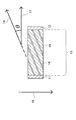
図1において、平行に配置された第1電極11と第2電極12によって積層体13を挟んだような構成で熱発電デバイス素子が形成されている。積層体13はPbTe層14と金属層15が交互に積層されて構成され、その層に平行な方向16は電極の対向方向17に対して角度θだけ傾斜している。
In FIG. 1, a thermoelectric device element is formed in such a configuration that a laminated
このように構成された熱発電デバイス素子を駆動する際に温度差を印加する、すなわち温度勾配が生じる方向18は電極の対向方向17に対して直交しており、発生した電力は第1電極11と第2電極12を介して取り出される。具体的には図2に示したように、熱発電デバイス素子21の電極を配置しない一方の面に高温部22を、他方の面に低温部23を密着させて熱発電デバイス素子に対して温度差を印加する。この構成において、温度勾配が生じる方向24は図2に示したように電極の対向方向に対して垂直となる。
A temperature difference is applied when driving the thermoelectric device element configured as described above, that is, the
π型構造を有する従来の熱発電デバイス素子では、温度差を印加する方向に対して平行方向だけに起電力が生じ、垂直方向に起電力が生じることは無い。詳細は後述する実施例で述べるが、本発明者等は様々な条件を検討し最適化することにより、積層体13の層に平行な方向16と電極の対向方向17とがなす角度、およびPbTe層14と金属層15の厚さおよびその比と熱発電性能の関係を詳細に調べて行く過程で、上記条件を適切に設定することにより本発明の熱発電デバイス素子において予想外に大きな熱発電性能が得られることを見出した。
In a conventional thermoelectric generator device element having a π-type structure, an electromotive force is generated only in the direction parallel to the direction in which the temperature difference is applied, and no electromotive force is generated in the vertical direction. Although details will be described in the examples described later, the present inventors have examined and optimized various conditions, and thereby, the angle formed between the
本発明の熱発電デバイス素子におけるPbTe層14は作製条件により組成ずれを生じることがあるが、Pb1Texと表記した場合にxが0.75<x<1.25の範囲にあれば良い。
The
本発明の熱発電デバイス素子における第1電極11および第2電極12は電気伝導の良い材料であれば特に限定されない。具体的にはCu、Ag、Mo、W、Al、Ti、Cr、Au、Pt、In等の金属またはTiN、スズ添加酸化インジウム(ITO)、SnO2等の窒化物または酸化物が良い。また、はんだや導電性ペーストを用いることもできる。
The 1st electrode 11 and the
積層体13を構成する金属層15は熱伝導率κが高く、かつ電気抵抗率が小さいものが良い。具体的にはCu、Ag、Au、Alあるいはこれらの材料からなる合金であるが、この中でもCu、Ag、Auが好ましく、CuとAgが特に好ましい。
The
本発明の熱発電デバイス素子の作製方法を図3を参照しながら説明する。 A method for producing the thermoelectric device element of the present invention will be described with reference to FIG.
積層体13を構成する積層構造体は、例えば金属32の箔の両面にPbTe系材料31を蒸着法により堆積したものを複数重ねて圧力をかけ、またさらに熱も加えて圧着成形して作製することができる。また、PbTe31と金属32の薄膜を交互に堆積して本デバイスにおける積層構造を作製することもできる。
The laminated structure constituting the laminated
次に、以上のようにして作製した積層構造体を切り出し、板状の積層体13に加工する。この際、図3の破線に示したように積層の向きが板状の積層体13の表面に対して所望の傾斜角度となるよう、切り出し範囲33を設定する。必要があれば切り出した積層体13に研磨処理を行っても良い。その後、板状の積層体13の、傾斜方向の一対の端面の一部あるいは全面に第1電極11および第2電極12を設けることにより、本発明の熱発電デバイス素子を得ることができる。
Next, the laminated structure produced as described above is cut out and processed into a plate-like laminated
本デバイスを構成する積層体13における金属層15とPbTe層14の厚みの比は20:1から400:1の範囲にあることが好ましい。この理由は、後述する実施例2からも理解されるように、この範囲外であると、パワーファクター(S2/ρ)の値が十分大きくならないからである。
The thickness ratio of the
また、積層体13の層に平行な方向16と電極の対向方向17とがなす角度θは10°から55°の範囲にあるように作製することが好ましく、15°から45°であることがより好ましい。この理由は、後述する実施例1からも理解されるように、10°未満または55°を超えると、パワーファクター(S2/ρ)の値が十分大きくならないからである。
The angle θ formed by the
金属層15を基体としてPbTe層14の薄膜を作製する際の作製方法は特に限定されないので、スパッタ法、蒸着法、レーザーアブレーション法、化学的気相成長法などの気相成長によるもの、あるいは液相からの成長など種々の方法が適用可能である。
The method for producing the thin film of the
第1電極11および第2電極12の作製方法は、蒸着法、スパッタ法などの気相成長の他に、導電性ペーストの塗布、めっき、溶射、はんだによる接合など様々な方法を用いることができる。
As a method for manufacturing the first electrode 11 and the
本発明の熱発電デバイス素子の作製方法は、本デバイス構造を実現する手法であれば特に上記方法に限定されるものではない。例えば金属板の表面に周期的に開口部を有するエッチングマスクを設け、金属板の表面に対して斜め方向から直進性の高いエッチング粒子を照射することによって、断面が金属板表面に対して傾斜したようなスリットが等間隔に並んだ構造を作製し、そのスリットの中にPbTeを蒸着あるいはめっきすることによって本発明の熱発電デバイス素子を作製することも可能である。 The method for producing the thermoelectric power generation device element of the present invention is not particularly limited to the above method as long as it is a method for realizing the device structure. For example, by providing an etching mask having openings periodically on the surface of the metal plate and irradiating the surface of the metal plate with etching particles having high straightness from an oblique direction, the cross section is inclined with respect to the surface of the metal plate. It is also possible to produce the thermoelectric device element of the present invention by producing a structure in which such slits are arranged at equal intervals and depositing or plating PbTe in the slit.
(実施の形態2)
図4は本発明の実施の形態2における熱発電デバイスの構成を示した図である。
(Embodiment 2)
FIG. 4 is a diagram showing the configuration of the thermoelectric generator device according to Embodiment 2 of the present invention.
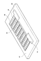
図4で示したのは、実施の形態1と同様の手順で作製される板状の積層体(熱発電デバイス素子)を、接続電極43を介して電気的に接続して平板状に構成したものである。このように構成される熱発電デバイスを用いて適用面積を大きくすることにより、全体としてより多くの発電量を得ることができる。
FIG. 4 shows that a plate-like laminate (thermoelectric device element) manufactured in the same procedure as in the first embodiment is electrically connected via the
本デバイスにおける接続電極43は電気伝導の良い材料であれば特に限定されない。具体的にはCu、Ag、Mo、W、Al、Ti、Cr、Au、Pt、In等の金属またはTiN、スズ添加酸化インジウム(ITO)、SnO2等の窒化物や酸化物が良い。また、はんだや導電性ペーストを用いることも可能である。作製方法は、蒸着法、スパッタ法などの気相成長の他にめっき、溶射など様々な方法を用いることができる。
The
このようにして作製される熱発電デバイスを駆動する際は、平板状のデバイスの一方の面に高温部、他方の面に低温部を密着して熱流を生じさせることによって温度差を印加する。熱流から本デバイスによって変換された電力は取り出し電極44を介して外部に取り出すことができる。
When driving the thermoelectric power generation device manufactured in this way, a temperature difference is applied by causing a high temperature part to adhere to one surface of the flat device and a low temperature part to the other surface to generate a heat flow. The electric power converted by the device from the heat flow can be extracted outside through the
本実施の形態における熱発電デバイスを構成するにあたり、積層体は接続電極43を介して電気的に直列に接続する他に、図5に示すように電気的に並列に接続しても良い。積層体を直列に接続する利点は、電力を取り出す際の電圧を大きくすることにある。積層体を並列に接続すると、熱発電デバイス全体の内部抵抗を小さくすることの他に、接続電極43による電気的な接続が一部断線してもデバイス全体としての電気的な接続を保つことにも利点がある。すなわち、これら直列および並列接続を適切に組み合わせる(例えば、図5を参照)ことによって、高い発電能力を有する熱発電デバイスを構成することができる。
In configuring the thermoelectric power generation device in the present embodiment, the laminates may be electrically connected in parallel as shown in FIG. 5 in addition to being electrically connected in series via the
(実施例)
以下、本発明のより具体的な実施例を説明する。
(Example)
Hereinafter, more specific examples of the present invention will be described.
(実施例1)
PbTe層と金属の積層体13として、幾つかの金属材料を用いて本発明の熱発電デバイス素子を作製した。金属とPbTeの積層体は、図3に示すように、金属箔の両面にPbTe薄膜を形成して得られたPbTe/金属箔/PbTeのシートを重ね合わせて加熱しながら圧着することにより作製した。第1電極11および第2電極12にはAuを用いた。金属箔としては、金、銀、銅、アルミの各種金属材料の素材の箔を用いた。
Example 1
As the PbTe layer and
まず100mm×100mm、厚さ99μmの金属箔の両面に真空蒸着法により膜厚0.5μmのPbTe薄膜を形成した後、5mm×50mmの大きさに切断して短冊状の小片を得た。 First, a PbTe thin film having a thickness of 0.5 μm was formed on both surfaces of a metal foil having a size of 100 mm × 100 mm and a thickness of 99 μm by a vacuum deposition method, and then cut into a size of 5 mm × 50 mm to obtain strip-shaped pieces.
真空蒸着法によるPbTe薄膜の作製条件は以下の通りである。まず原料のPbTeバルク結晶を、真空容器内に設置されているタングステンボートに配置した。タングステンボートに対向して、真空容器内に金属箔を配置した。真空容器内を10-3Pa以下まで排気した後、真空容器内に設置してあるハロゲンランプにより金属箔を300℃に加熱した状態で、タングステンボートに電流を印加してPbTe薄膜を蒸着した。この時、薄膜の膜厚は水晶振動子膜厚モニターによって随時計測し、目的の膜厚になるよう蒸着時間を制御した。金属箔の片面に0.5μmのPbTe薄膜の形成が完了した後、金属箔を裏返し、逆側にも同様の手順で0.5μmのPbTe薄膜を形成した。 The conditions for producing the PbTe thin film by the vacuum deposition method are as follows. First, a raw material PbTe bulk crystal was placed in a tungsten boat installed in a vacuum vessel. A metal foil was placed in the vacuum vessel facing the tungsten boat. After evacuating the inside of the vacuum vessel to 10 −3 Pa or less, a PbTe thin film was deposited by applying current to the tungsten boat while the metal foil was heated to 300 ° C. with a halogen lamp installed in the vacuum vessel. At this time, the thickness of the thin film was measured at any time with a crystal oscillator thickness monitor, and the deposition time was controlled so as to achieve the desired thickness. After the formation of the 0.5 μm PbTe thin film on one side of the metal foil was completed, the metal foil was turned over and a 0.5 μm PbTe thin film was formed on the opposite side in the same procedure.
このようにして作製したPbTe薄膜の組成をエネルギー分散型X線解析法により測定した。その結果、PbとTeの組成はほぼ1:1であることを確認した。またX線回折測定ではPbTeと同一の結晶構造を有していることを確認した。同様の工程を繰り返した後、この小片を200枚重ね合わせ、積層方向に100kg/cm2の荷重をかけながら10-4Paの減圧下において250℃で1時間、加熱しながら圧着を行った。圧着後、おおよそ5mm×50mm×20mmの積層構造体を得た。この積層構造体に対して、切削研磨を行い、3mm×48mm×20mmの積層構造体を得た。積層断面を走査電子顕微鏡にて観察したところ、金属層が約99μm、PbTeが約1μmの厚さで周期的に積層しているのを確認した。 The composition of the PbTe thin film thus produced was measured by an energy dispersive X-ray analysis method. As a result, it was confirmed that the composition of Pb and Te was approximately 1: 1. Further, it was confirmed by X-ray diffraction measurement that it had the same crystal structure as PbTe. After repeating the same process, 200 pieces of this small piece were overlapped and pressure-bonded while heating at 250 ° C. for 1 hour under a reduced pressure of 10 −4 Pa while applying a load of 100 kg / cm 2 in the stacking direction. After crimping, a laminated structure of approximately 5 mm × 50 mm × 20 mm was obtained. The laminated structure was cut and polished to obtain a laminated structure of 3 mm × 48 mm × 20 mm. When the cross section of the laminate was observed with a scanning electron microscope, it was confirmed that the metal layer was periodically laminated with a thickness of about 99 μm and PbTe of about 1 μm.
こうして得られた積層構造体に対して、ダイヤモンドカッターを用いた切削加工で積層周期に対して図3に示したように15°間隔の角度で傾斜をつけて平板状に切り出した。平板の厚みは1mmとし、幅3mmで長さ20mmの平板を0°から90°までの範囲の各傾斜角度(θ)に対して作製した。その後スパッタ法により長辺の両端にAuからなる電極を形成し、図1に示したような構造のデバイスを作製した。 The laminated structure thus obtained was cut into a flat plate with an inclination of 15 ° intervals with respect to the lamination period by cutting using a diamond cutter as shown in FIG. The thickness of the flat plate was 1 mm, and a flat plate having a width of 3 mm and a length of 20 mm was prepared for each inclination angle (θ) in the range from 0 ° to 90 °. Thereafter, electrodes made of Au were formed on both ends of the long side by sputtering, and a device having a structure as shown in FIG. 1 was produced.
作製した試料に対して発電性能の評価を行った。図2に示すように平板デバイスの片側をヒータで150℃に加熱し、もう片側を水冷で30℃に冷却して端子間の起電圧と電気抵抗を測定した。銀箔を用いて30°傾斜させたデバイスの場合、起電圧201mVで抵抗は0.77mΩであった。これよりパワーファクターは604μW/cmK2と見積もられた。同様の手順で、各金属材料を用いた傾斜角度の異なるデバイスの性能を測定したところ、表1の結果となった。 The power generation performance was evaluated for the prepared samples. As shown in FIG. 2, one side of the flat plate device was heated to 150 ° C. with a heater, the other side was cooled to 30 ° C. with water cooling, and the electromotive voltage and electrical resistance between the terminals were measured. In the case of a device tilted 30 ° using silver foil, the electromotive force was 201 mV and the resistance was 0.77 mΩ. From this, the power factor was estimated to be 604 μW / cmK 2 . When the performance of devices having different inclination angles using each metal material was measured in the same procedure, the results shown in Table 1 were obtained.

以上の結果から、各金属材料に関してほぼ共通に傾斜角度が15°〜45°の時に、現在実用化されているBi2Te3を用いたπ型素子の10倍程度以上の優れたデバイス特性が得られることが判った。特に金属材料として、銀あるいは銅を用いた場合、他の金属に比べて性能が高いことが確認された。 From the above results, when the inclination angle is 15 ° to 45 ° almost in common with each metal material, the device characteristics are about 10 times or more superior to the π-type element using Bi 2 Te 3 which is currently in practical use. It turns out that it is obtained. In particular, when silver or copper was used as the metal material, it was confirmed that the performance was higher than that of other metals.
(実施例2)
実施例1と同様の手法で、金属箔として20μmの銅箔を用い、積層デバイスを構成した。20μmのCu箔の両面にPbTe薄膜を膜厚変化させて形成、減圧下で加熱圧着して、Cu層の厚みが20μm、PbTe層の厚みが0.05μmから4μmまで変化したCu/PbTe積層構造を作製した。 25°の平板状に切り出して作製した厚み1mm、幅3mm、長さ20mmの熱発電デバイス素子のパワーファクターの測定結果は表2のようになった。
(Example 2)
In the same manner as in Example 1, a 20 μm copper foil was used as the metal foil to form a laminated device. A Cu / PbTe laminated structure in which a PbTe thin film is formed on both sides of a 20 μm Cu foil by changing the film thickness, heat-pressed under reduced pressure, the Cu layer thickness is changed to 20 μm, and the PbTe layer thickness is changed from 0.05 μm to 4 μm Was made. Table 2 shows the measurement results of the power factor of a thermoelectric device element having a thickness of 1 mm, a width of 3 mm, and a length of 20 mm produced by cutting into a 25 ° flat plate.
この結果、PbTe層厚に関して0.05μmから1μmの範囲で従来の10倍程度以上の優れたデバイス性能が得られたことが確認された。これは全体の積層周期におけるCu:PbTeの比が400:1から20:1の範囲にある時に好ましい結果となることを示したものであり、特に100:1から80:1の範囲(PbTe層の割合が約1%の近傍)の時に最も優れた性能が得られたことが確認された。 As a result, it was confirmed that an excellent device performance of about 10 times or more of the conventional device performance was obtained in the range of 0.05 μm to 1 μm with respect to the PbTe layer thickness. This indicates that favorable results are obtained when the ratio of Cu: PbTe in the entire stacking cycle is in the range of 400: 1 to 20: 1, particularly in the range of 100: 1 to 80: 1 (PbTe layer). It was confirmed that the most excellent performance was obtained when the ratio of (1) was about 1%.
(実施例3)
金属箔として20μmの銅箔を用い、実施例1と同様の手法で積層デバイスを構成した。20μmのCu箔の両面に、PbTe薄膜を0.1μm形成した後、加熱圧着し、PbTe層厚が0.2μmのCu/PbTe積層構造(膜厚比率100:1)を作製した。切り出し角度を10°から55°の範囲で5°ごとに設定してデバイスを作製し、パワーファクターを測定したところ、表3の結果が得られた。
(Example 3)
A laminated device was constructed in the same manner as in Example 1 using a 20 μm copper foil as the metal foil. A PbTe thin film having a thickness of 0.1 μm was formed on both sides of a 20 μm Cu foil, followed by thermocompression bonding to produce a Cu / PbTe laminated structure (film thickness ratio 100: 1) having a PbTe layer thickness of 0.2 μm. A device was prepared by setting the cut-out angle every 5 ° in the range of 10 ° to 55 °, and the power factor was measured. The results shown in Table 3 were obtained.
Cu/PbTe積層デバイスの傾斜角度に関して検討した結果、性能に優れる10°から55°の範囲の中でも特に15〜45°の際に500μW/cmK2を超えることが確認され、現在実用化されているBi2Te3用いたπ型構造素子の10倍程度以上の高性能熱発電デバイス素子が実現した。 As a result of examining the inclination angle of the Cu / PbTe laminated device, it was confirmed that it exceeded 500 μW / cmK 2 especially in the range of 15 to 45 ° in the range of 10 ° to 55 ° which is excellent in performance, and is currently in practical use. A high-performance thermoelectric power generation device element of about 10 times or more of the π-type structure element using Bi 2 Te 3 was realized.
(実施例4)
実装面積をより広くし、さらに多くの発電量を得るために、金属42、接続電極43、取り出し電極44としてCuを用いた、図4に示したような熱発電デバイスを作製した。
Example 4
In order to increase the mounting area and obtain a larger amount of power generation, a thermoelectric power generation device as shown in FIG. 4 using Cu as the
CuとPbTeからなる積層体は実施例1と同様の手順で作製した。Cuが20μm厚でPbTeが0.2μm厚、すなわちCuとPbTeの積層方向の厚さの比が100:1になるように積層体を構成し、かつ傾斜角は25°とした。積層体の寸法は長さ50mm×幅3mm×厚さ0.5mmとしたものを合計15個作製した。また、接続電極43および取り出し電極44のCuは厚さ0.5mmの板を使用した。
A laminate made of Cu and PbTe was produced in the same procedure as in Example 1. The laminate was configured such that Cu was 20 μm thick and PbTe was 0.2 μm thick, that is, the thickness ratio of Cu and PbTe in the stacking direction was 100: 1, and the tilt angle was 25 °. A total of 15 laminates with a length of 50 mm, a width of 3 mm, and a thickness of 0.5 mm were produced. In addition, a plate having a thickness of 0.5 mm was used as Cu for the
作製した15個の積層体をアルミナからなる支持体46上に1mm間隔で配列し、接続電極43および取り出し電極44を少量のIn片を用い加熱圧着することによって電気的に直列接続した。この際、熱流による起電力が相殺されないよう、図4に示したように隣り合う積層体の傾斜構造は互いに逆向きになるように配置し、約60mm×60mmの熱発電デバイスを作製した。取り出し電極44間の抵抗値を測定したところ、125mΩであった。
The 15 prepared laminates were arranged on a support 46 made of alumina at an interval of 1 mm, and the
以上の手順で作製した本実施例の熱発電デバイスの発電特性を評価した。支持体46を裏面から水冷し、低温部とした。本デバイスの他方の面に高温部となるセラミックヒーターを密着させた。このような構成で低温部を25℃、高温部を40℃に保持したところ、開放端起電力は1.94Vとなり、パワーファクターを見積もると594μW/cmK2という高い値が得られた。この結果、本デバイスから最大10Wの電力を取り出すことができた。 The power generation characteristics of the thermoelectric power generation device of this example produced by the above procedure were evaluated. The support 46 was cooled with water from the back surface to form a low temperature part. A ceramic heater serving as a high temperature part was adhered to the other surface of the device. When the low temperature part was kept at 25 ° C. and the high temperature part was kept at 40 ° C. with such a configuration, the open-ended electromotive force was 1.94 V, and a high value of 594 μW / cmK 2 was obtained when the power factor was estimated. As a result, a maximum of 10 W of power could be extracted from this device.
本発明にかかる熱発電デバイス素子は、優れた発電特性を有しており、自動車や工場から排出される排ガスなどの熱を用いた発電機として利用可能である。 The thermoelectric power generation device element according to the present invention has excellent power generation characteristics and can be used as a power generator using heat such as exhaust gas discharged from an automobile or a factory.
また、小型の携帯発電機などの用途にも応用できる。 It can also be applied to small portable generators.
11 第1電極
12 第2電極
13 積層体
14 PbTe層
15 金属層
16 層に平行な方向
17 電極の対向方向
18 温度勾配が生じる方向
21 熱発電デバイス素子
22 高温部
23 低温部
24 温度勾配が生じる方向
31 PbTe
32 金属
33 切り出し範囲
41 PbTe
42 金属
43 接続電極
44 取り出し電極
45 支持体
DESCRIPTION OF SYMBOLS 11
32
42
Claims (15)
前記第1電極に対向する第2電極と、
前記第1電極および前記第2電極との間に挟まれ、かつ前記第1電極および前記第2電極のいずれにも電気的に接続された積層体とを具備し、
前記積層体は、PbTe層と金属層とが交互に積層されてなり、
前記PbTe層および前記金属層が、前記第1電極と前記第2電極とが対向する方向に対して角度θで傾斜しており、
前記角度θが10°以上55°以下であり、
前記金属層が、Al、Cu、Ag、またはAuからなり、
前記金属層の厚み:前記PbTe層の厚みの比が400:1から20:1までの範囲内にあり、
前記対向する方向に対して垂直方向に温度差を印加することによって、前記第1電極および前記第2電極を介して電力を取り出す、熱発電デバイス素子。 A first electrode;
A second electrode facing the first electrode;
A laminated body sandwiched between the first electrode and the second electrode and electrically connected to both the first electrode and the second electrode;
The laminate is formed by alternately laminating PbTe layers and metal layers,
The PbTe layer and the metal layer are inclined at an angle θ with respect to a direction in which the first electrode and the second electrode face each other;
The angle θ is 10 ° to 55 °,
The metal layer is made of Al, Cu, Ag, or Au;
The ratio of the thickness of the metal layer to the thickness of the PbTe layer is in the range of 400: 1 to 20: 1,
Wherein by applying a temperature difference in a direction perpendicular to the opposing direction, takes out the power by through the first electrode and the second electrode, the heat generating device element.
請求項1に記載の熱発電デバイス素子。 The angle θ is 15 ° or more and 45 ° or less,
The thermoelectric power generation device element according to claim 1.
請求項1に記載の熱発電デバイス素子。 The metal layer is made of Cu, Ag, or Au;
The thermoelectric power generation device element according to claim 1.
請求項3に記載の熱発電デバイス素子。 The metal layer is made of Cu or Ag;
The thermoelectric power generation device element according to claim 3.
請求項1に記載の熱発電デバイス素子。 The ratio of the thickness of the metal layer to the thickness of the PbTe layer is in the range of 100: 1 to 80: 1.
The thermoelectric power generation device element according to claim 1.
前記金属層の厚み:前記PbTe層の厚みの比が100:1から80:1までの範囲内にある、
請求項2に記載の熱発電デバイス素子。 The metal layer is made of Cu or Ag;
The ratio of the thickness of the metal layer to the thickness of the PbTe layer is in the range of 100: 1 to 80: 1.
The thermoelectric power generation device element according to claim 2.
前記第1電極に対向する第2電極と、
前記第1電極および前記第2電極との間に挟まれ、かつ前記第1電極および前記第2電極のいずれにも電気的に接続された積層体とを具備し、
前記積層体は、PbTe層と金属層とが交互に積層されてなり、
前記PbTe層および前記金属層が、前記第1電極と前記第2電極とが対向する方向に対して角度θで傾斜しており、
前記角度θが10°以上55°以下であり、
前記金属層が、Al、Cu、Ag、またはAuからなり、
前記金属層の厚み:前記PbTe層の厚みの比が400:1から20:1までの範囲内にあり、
前記対向する方向に対して垂直方向に温度差を印加することによって、前記第1電極および前記第2電極を介して電力を取り出す、熱発電デバイス素子の製造方法であって、
前記製造方法は、以下の工程を有する:
PbTe層と金属層とを交互に積層してなる積層構造体を得る積層構造体形成工程、
前記積層構造体の積層方向に対して傾斜する面で前記積層構造体を切り出して前記積層体を得る積層体切り出し工程、
前記積層体に前記第1電極および前記第2電極を形成する電極形成工程。 A first electrode;
A second electrode facing the first electrode;
A laminated body sandwiched between the first electrode and the second electrode and electrically connected to both the first electrode and the second electrode;
The laminate is formed by alternately laminating PbTe layers and metal layers,
The PbTe layer and the metal layer are inclined at an angle θ with respect to a direction in which the first electrode and the second electrode face each other;
The angle θ is 10 ° to 55 °,
The metal layer is made of Al, Cu, Ag, or Au;
The ratio of the thickness of the metal layer to the thickness of the PbTe layer is in the range of 400: 1 to 20: 1,
Wherein by applying a temperature difference in a direction perpendicular to the opposing direction, takes out the power by through the first electrode and the second electrode, a manufacturing method of the thermoelectric device element,
The manufacturing method has the following steps:
A laminated structure forming step for obtaining a laminated structure in which PbTe layers and metal layers are alternately laminated;
A laminate cutout step of obtaining the laminate by cutting out the laminate structure on a surface inclined with respect to the lamination direction of the laminate structure;
An electrode forming step of forming the first electrode and the second electrode on the laminate;
前記第1電極に対向する第2電極と、
前記第1電極および前記第2電極との間に挟まれ、かつ前記第1電極および前記第2電極のいずれにも電気的に接続された積層体とを具備し、
前記積層体は、PbTe層と金属層とが交互に積層されてなり、
前記PbTe層および前記金属層が、前記第1電極と前記第2電極とが対向する方向に対して角度θで傾斜しており、前記角度θが15°以上45°以下であり、前記金属層が、Al、Cu、Ag、またはAuからなり、前記金属層の厚み:前記PbTe層の厚みの比が400:1から20:1までの範囲内にある熱発電デバイス素子から、前記第1電極および前記第2電極を介して電力を取り出す発電方法であって、
前記発電方法は以下の工程を包含する:
前記対向する方向に対して垂直方向に温度差を印加する、温度差印加工程。 A first electrode;
A second electrode facing the first electrode;
A laminated body sandwiched between the first electrode and the second electrode and electrically connected to both the first electrode and the second electrode;
The laminate is formed by alternately laminating PbTe layers and metal layers,
The PbTe layer and the metal layer are inclined at an angle θ with respect to a direction in which the first electrode and the second electrode face each other, and the angle θ is 15 ° or more and 45 ° or less, and the metal layer From the thermoelectric device element in which the ratio of the thickness of the metal layer to the thickness of the PbTe layer is in the range of 400: 1 to 20: 1, and is made of Al, Cu, Ag, or Au. and a power generation method draw power and through the second electrode,
The power generation method includes the following steps:
Applying a temperature difference in a direction perpendicular to the opposing direction;
請求項8に記載の発電方法。 The angle θ is 15 ° or more and 45 ° or less,
The power generation method according to claim 8.
請求項8に記載の発電方法。 The metal layer is made of Cu, Ag, or Au;
The power generation method according to claim 8.
請求項10に記載の発電方法。 The metal layer is made of Cu or Ag;
The power generation method according to claim 10.
請求項8に記載の発電方法。 The ratio of the thickness of the metal layer to the thickness of the PbTe layer is in the range of 100: 1 to 80: 1.
The power generation method according to claim 8.
前記金属層の厚み:前記PbTe層の厚みの比が100:1から80:1までの範囲内にある、
請求項9に記載の発電方法。 The metal layer is made of Cu or Ag;
The ratio of the thickness of the metal layer to the thickness of the PbTe layer is in the range of 100: 1 to 80: 1.
The power generation method according to claim 9.
前記支持板上に設けられた複数個の熱発電デバイス素子と、
を具備し、
ここで、前記各熱発電デバイス素子は、請求項1に係る熱発電デバイス素子であり、
隣接する2つの前記熱発電デバイス素子の一端を電気的に接続する各接続電極によって前記複数個の熱発電デバイス素子が電気的に直列に接続されており、
電気的に直列に接続されている前記複数個の熱発電デバイス素子の2つの終端には、それぞれ取り出し電極が接続されており、
前記支持板の法線方向に沿って温度差が印加されることによって、前記取り出し電極を介して電力が取り出される、熱発電デバイス。 A support plate;
A plurality of thermoelectric device elements provided on the support plate;
Comprising
Here, each of the thermoelectric generation device elements is a thermoelectric generation device element according to claim 1,
The plurality of thermoelectric generation device elements are electrically connected in series by each connection electrode that electrically connects one end of two adjacent thermoelectric generation device elements,
An extraction electrode is connected to each of the two ends of the plurality of thermoelectric device elements that are electrically connected in series,
A thermoelectric generation device in which electric power is extracted through the extraction electrode when a temperature difference is applied along a normal direction of the support plate.
前記支持板上に設けられた複数個の熱発電デバイス素子とを具備し、
ここで、前記各熱発電デバイス素子は、請求項1に係る熱発電デバイス素子であり、
各熱発電デバイス素子の両端をそれぞれ電気的に接続する2つの取り出し電極によって前記複数個の熱発電デバイス素子が電気的に並列に接続されており、
前記支持板の法線方向に沿って温度差が印加されることによって、前記取り出し電極を介して電力が取り出される、熱発電デバイス。
A support plate;
A plurality of thermoelectric device elements provided on the support plate;
Here, each of the thermoelectric generation device elements is a thermoelectric generation device element according to claim 1,
The plurality of thermoelectric device elements are electrically connected in parallel by two extraction electrodes that electrically connect both ends of each thermoelectric device element,
A thermoelectric generation device in which electric power is extracted through the extraction electrode when a temperature difference is applied along a normal direction of the support plate.
Priority Applications (1)
| Application Number | Priority Date | Filing Date | Title |
|---|---|---|---|
| JP2008052993A JP5176602B2 (en) | 2008-03-04 | 2008-03-04 | Thermoelectric device element |
Applications Claiming Priority (1)
| Application Number | Priority Date | Filing Date | Title |
|---|---|---|---|
| JP2008052993A JP5176602B2 (en) | 2008-03-04 | 2008-03-04 | Thermoelectric device element |
Publications (3)
| Publication Number | Publication Date |
|---|---|
| JP2009212267A JP2009212267A (en) | 2009-09-17 |
| JP2009212267A5 JP2009212267A5 (en) | 2010-09-30 |
| JP5176602B2 true JP5176602B2 (en) | 2013-04-03 |
Family
ID=41185138
Family Applications (1)
| Application Number | Title | Priority Date | Filing Date |
|---|---|---|---|
| JP2008052993A Active JP5176602B2 (en) | 2008-03-04 | 2008-03-04 | Thermoelectric device element |
Country Status (1)
| Country | Link |
|---|---|
| JP (1) | JP5176602B2 (en) |
Families Citing this family (1)
| Publication number | Priority date | Publication date | Assignee | Title |
|---|---|---|---|---|
| JP6904847B2 (en) * | 2017-08-10 | 2021-07-21 | 太陽誘電株式会社 | Laminated pyroelectric element |
Family Cites Families (2)
| Publication number | Priority date | Publication date | Assignee | Title |
|---|---|---|---|---|
| DE4434904A1 (en) * | 1994-09-29 | 1996-06-05 | Max Planck Gesellschaft | Highly sensitive thermo-electric radiation detector |
| JPH1074986A (en) * | 1996-06-27 | 1998-03-17 | Natl Aerospace Lab | Production of thermoelectric conversion element, pi-type thermoelectric conversion element pair and thermoelectric conversion module |
-
2008
- 2008-03-04 JP JP2008052993A patent/JP5176602B2/en active Active
Also Published As
| Publication number | Publication date |
|---|---|
| JP2009212267A (en) | 2009-09-17 |
Similar Documents
| Publication | Publication Date | Title |
|---|---|---|
| JP4078392B1 (en) | Power generation method using thermoelectric power generation element, thermoelectric power generation element and manufacturing method thereof, and thermoelectric power generation device | |
| JP4124807B1 (en) | Power generation method using thermoelectric power generation element, thermoelectric power generation element and manufacturing method thereof, and thermoelectric power generation device | |
| US7449628B2 (en) | Electric power generation method using thermoelectric power generation element, thermoelectric power generation element and method of producing the same, and thermoelectric power generation device | |
| WO2010058553A1 (en) | Thermoelectric element and thermoelectric device | |
| WO2010007729A1 (en) | Method of manufacturing a thermoelectric device | |
| JP5176610B2 (en) | Thermoelectric device element | |
| JP4584355B2 (en) | Thermoelectric power generation device and power generation method using the same | |
| JP5176602B2 (en) | Thermoelectric device element | |
| JP5176609B2 (en) | Thermoelectric device element | |
| JP5176607B2 (en) | Thermoelectric device element | |
| JP5176608B2 (en) | Thermoelectric device element | |
| JP5200884B2 (en) | Thermoelectric power generation device | |
| JP5176606B2 (en) | Thermoelectric device element | |
| WO2012120572A1 (en) | Electricity generation method using thermoelectric generation element, thermoelectric generation element and manufacturing method thereof, and thermoelectric generation device | |
| JP5200885B2 (en) | Thermoelectric power generation device | |
| JP5200883B2 (en) | Thermoelectric power generation device | |
| JP4130845B1 (en) | Power generation method using thermoelectric power generation element, thermoelectric power generation element and manufacturing method thereof, and thermoelectric power generation device |
Legal Events
| Date | Code | Title | Description |
|---|---|---|---|
| A621 | Written request for application examination |
Free format text: JAPANESE INTERMEDIATE CODE: A621 Effective date: 20100817 |
|
| A521 | Request for written amendment filed |
Free format text: JAPANESE INTERMEDIATE CODE: A523 Effective date: 20100818 |
|
| RD01 | Notification of change of attorney |
Free format text: JAPANESE INTERMEDIATE CODE: A7421 Effective date: 20100914 |
|
| A977 | Report on retrieval |
Free format text: JAPANESE INTERMEDIATE CODE: A971007 Effective date: 20120223 |
|
| A131 | Notification of reasons for refusal |
Free format text: JAPANESE INTERMEDIATE CODE: A131 Effective date: 20120327 |
|
| A601 | Written request for extension of time |
Free format text: JAPANESE INTERMEDIATE CODE: A601 Effective date: 20120523 |
|
| A602 | Written permission of extension of time |
Free format text: JAPANESE INTERMEDIATE CODE: A602 Effective date: 20120528 |
|
| A521 | Request for written amendment filed |
Free format text: JAPANESE INTERMEDIATE CODE: A523 Effective date: 20120622 |
|
| TRDD | Decision of grant or rejection written | ||
| A01 | Written decision to grant a patent or to grant a registration (utility model) |
Free format text: JAPANESE INTERMEDIATE CODE: A01 Effective date: 20121211 |
|
| A61 | First payment of annual fees (during grant procedure) |
Free format text: JAPANESE INTERMEDIATE CODE: A61 Effective date: 20121224 |
|
| R151 | Written notification of patent or utility model registration |
Ref document number: 5176602 Country of ref document: JP Free format text: JAPANESE INTERMEDIATE CODE: R151 |
|
| FPAY | Renewal fee payment (event date is renewal date of database) |
Free format text: PAYMENT UNTIL: 20160118 Year of fee payment: 3 |