JP5175285B2 - Method for controlling morphology during epitaxial layer formation - Google Patents
Method for controlling morphology during epitaxial layer formationInfo
- Publication number
- JP5175285B2 JP5175285B2 JP2009522826A JP2009522826A JP5175285B2 JP 5175285 B2 JP5175285 B2 JP 5175285B2 JP 2009522826 A JP2009522826 A JP 2009522826A JP 2009522826 A JP2009522826 A JP 2009522826A JP 5175285 B2 JP5175285 B2 JP 5175285B2
- Authority
- JP
- Japan
- Prior art keywords
- substrate
- deposition
- dichlorosilane
- etching
- silane
- Prior art date
- Legal status (The legal status is an assumption and is not a legal conclusion. Google has not performed a legal analysis and makes no representation as to the accuracy of the status listed.)
- Expired - Fee Related
Links
Images

Classifications
-
- H—ELECTRICITY
- H01—ELECTRIC ELEMENTS
- H01L—SEMICONDUCTOR DEVICES NOT COVERED BY CLASS H10
- H01L21/00—Processes or apparatus adapted for the manufacture or treatment of semiconductor or solid state devices or of parts thereof
- H01L21/02—Manufacture or treatment of semiconductor devices or of parts thereof
- H01L21/04—Manufacture or treatment of semiconductor devices or of parts thereof the devices having at least one potential-jump barrier or surface barrier, e.g. PN junction, depletion layer or carrier concentration layer
- H01L21/34—Manufacture or treatment of semiconductor devices or of parts thereof the devices having at least one potential-jump barrier or surface barrier, e.g. PN junction, depletion layer or carrier concentration layer the devices having semiconductor bodies not provided for in groups H01L21/0405, H01L21/0445, H01L21/06, H01L21/16 and H01L21/18 with or without impurities, e.g. doping materials
-
- H—ELECTRICITY
- H01—ELECTRIC ELEMENTS
- H01L—SEMICONDUCTOR DEVICES NOT COVERED BY CLASS H10
- H01L21/00—Processes or apparatus adapted for the manufacture or treatment of semiconductor or solid state devices or of parts thereof
- H01L21/02—Manufacture or treatment of semiconductor devices or of parts thereof
- H01L21/02104—Forming layers
- H01L21/02365—Forming inorganic semiconducting materials on a substrate
- H01L21/02367—Substrates
- H01L21/0237—Materials
- H01L21/02373—Group 14 semiconducting materials
- H01L21/02381—Silicon, silicon germanium, germanium
-
- C—CHEMISTRY; METALLURGY
- C30—CRYSTAL GROWTH
- C30B—SINGLE-CRYSTAL GROWTH; UNIDIRECTIONAL SOLIDIFICATION OF EUTECTIC MATERIAL OR UNIDIRECTIONAL DEMIXING OF EUTECTOID MATERIAL; REFINING BY ZONE-MELTING OF MATERIAL; PRODUCTION OF A HOMOGENEOUS POLYCRYSTALLINE MATERIAL WITH DEFINED STRUCTURE; SINGLE CRYSTALS OR HOMOGENEOUS POLYCRYSTALLINE MATERIAL WITH DEFINED STRUCTURE; AFTER-TREATMENT OF SINGLE CRYSTALS OR A HOMOGENEOUS POLYCRYSTALLINE MATERIAL WITH DEFINED STRUCTURE; APPARATUS THEREFOR
- C30B25/00—Single-crystal growth by chemical reaction of reactive gases, e.g. chemical vapour-deposition growth
- C30B25/02—Epitaxial-layer growth
-
- C—CHEMISTRY; METALLURGY
- C30—CRYSTAL GROWTH
- C30B—SINGLE-CRYSTAL GROWTH; UNIDIRECTIONAL SOLIDIFICATION OF EUTECTIC MATERIAL OR UNIDIRECTIONAL DEMIXING OF EUTECTOID MATERIAL; REFINING BY ZONE-MELTING OF MATERIAL; PRODUCTION OF A HOMOGENEOUS POLYCRYSTALLINE MATERIAL WITH DEFINED STRUCTURE; SINGLE CRYSTALS OR HOMOGENEOUS POLYCRYSTALLINE MATERIAL WITH DEFINED STRUCTURE; AFTER-TREATMENT OF SINGLE CRYSTALS OR A HOMOGENEOUS POLYCRYSTALLINE MATERIAL WITH DEFINED STRUCTURE; APPARATUS THEREFOR
- C30B29/00—Single crystals or homogeneous polycrystalline material with defined structure characterised by the material or by their shape
- C30B29/02—Elements
- C30B29/06—Silicon
-
- H—ELECTRICITY
- H01—ELECTRIC ELEMENTS
- H01L—SEMICONDUCTOR DEVICES NOT COVERED BY CLASS H10
- H01L21/00—Processes or apparatus adapted for the manufacture or treatment of semiconductor or solid state devices or of parts thereof
- H01L21/02—Manufacture or treatment of semiconductor devices or of parts thereof
- H01L21/02104—Forming layers
- H01L21/02365—Forming inorganic semiconducting materials on a substrate
- H01L21/02518—Deposited layers
- H01L21/02521—Materials
- H01L21/02524—Group 14 semiconducting materials
- H01L21/02532—Silicon, silicon germanium, germanium
-
- H—ELECTRICITY
- H01—ELECTRIC ELEMENTS
- H01L—SEMICONDUCTOR DEVICES NOT COVERED BY CLASS H10
- H01L21/00—Processes or apparatus adapted for the manufacture or treatment of semiconductor or solid state devices or of parts thereof
- H01L21/02—Manufacture or treatment of semiconductor devices or of parts thereof
- H01L21/02104—Forming layers
- H01L21/02365—Forming inorganic semiconducting materials on a substrate
- H01L21/02612—Formation types
- H01L21/02617—Deposition types
- H01L21/0262—Reduction or decomposition of gaseous compounds, e.g. CVD
-
- H—ELECTRICITY
- H01—ELECTRIC ELEMENTS
- H01L—SEMICONDUCTOR DEVICES NOT COVERED BY CLASS H10
- H01L21/00—Processes or apparatus adapted for the manufacture or treatment of semiconductor or solid state devices or of parts thereof
- H01L21/02—Manufacture or treatment of semiconductor devices or of parts thereof
- H01L21/02104—Forming layers
- H01L21/02365—Forming inorganic semiconducting materials on a substrate
- H01L21/02612—Formation types
- H01L21/02617—Deposition types
- H01L21/02636—Selective deposition, e.g. simultaneous growth of mono- and non-monocrystalline semiconductor materials
- H01L21/02639—Preparation of substrate for selective deposition
-
- H—ELECTRICITY
- H01—ELECTRIC ELEMENTS
- H01L—SEMICONDUCTOR DEVICES NOT COVERED BY CLASS H10
- H01L21/00—Processes or apparatus adapted for the manufacture or treatment of semiconductor or solid state devices or of parts thereof
- H01L21/02—Manufacture or treatment of semiconductor devices or of parts thereof
- H01L21/02104—Forming layers
- H01L21/02365—Forming inorganic semiconducting materials on a substrate
- H01L21/02656—Special treatments
- H01L21/02658—Pretreatments
- H01L21/02661—In-situ cleaning
-
- H—ELECTRICITY
- H01—ELECTRIC ELEMENTS
- H01L—SEMICONDUCTOR DEVICES NOT COVERED BY CLASS H10
- H01L21/00—Processes or apparatus adapted for the manufacture or treatment of semiconductor or solid state devices or of parts thereof
- H01L21/02—Manufacture or treatment of semiconductor devices or of parts thereof
- H01L21/04—Manufacture or treatment of semiconductor devices or of parts thereof the devices having at least one potential-jump barrier or surface barrier, e.g. PN junction, depletion layer or carrier concentration layer
- H01L21/18—Manufacture or treatment of semiconductor devices or of parts thereof the devices having at least one potential-jump barrier or surface barrier, e.g. PN junction, depletion layer or carrier concentration layer the devices having semiconductor bodies comprising elements of Group IV of the Periodic System or AIIIBV compounds with or without impurities, e.g. doping materials
- H01L21/20—Deposition of semiconductor materials on a substrate, e.g. epitaxial growth solid phase epitaxy
Description
本願は、2006年7月31日に出願された米国特許仮出願第60/820,956号からの優先権を主張し、その全てが参考として本願に組み込まれる。 This application claims priority from US Provisional Application No. 60 / 820,956, filed July 31, 2006, all of which are incorporated herein by reference.
本願は、以下の共同出願に関連しており、各出願は、その全てが参考として本願に組み込まれる。
・2004年12月1日に出願された米国特許出願第11/001,774号(ドケット番号第9618号)
・2005年9月14日に出願された米国特許出願第11/227,974号(ドケット番号第9618号/P01)
The present application is related to the following joint applications, each of which is incorporated herein by reference in its entirety:
・ US patent application No. 11 / 001,774 filed Dec. 1, 2004 (Docket No. 9618)
-U.S. Patent Application No. 11 / 227,974 (Docket No. 9618 / P01) filed on September 14, 2005
本発明は、半導体装置の製造に関連しており、より具体的には、エピタキシャル層形成中の形態(morphology)制御方法に関する。 The present invention relates to the manufacture of semiconductor devices, and more specifically to a method for controlling the morphology during epitaxial layer formation.
より小型のトランジスタが製造されるにつれて、超浅型ソース/ドレイン接合の生成がより手腕を問われるものになりつつある。概して、サブ100nm CMOS(相補型金属酸化膜半導体)デバイスは接合深さが30nm未満である必要がある。選択エピタキシャル堆積はしばしば、シリコン含有材料(例えば、Si、SiGeおよびSiC)のエピ層を接合に形成するために利用される。概して、選択エピタキシャル堆積は、誘電エリアでの成長なくシリコン堀(moats)におけるエピ層の成長を可能にする。選択エピタキシは、エレベーテッドソース/ドレイン、ソース/ドレイン延長部、コンタクトプラグ、あるいはバイポーラデバイスのベース層堆積などの半導体デバイス内で使用可能である。 As smaller transistors are manufactured, the creation of ultra-shallow source / drain junctions is becoming more challenging. In general, sub-100 nm CMOS (complementary metal oxide semiconductor) devices should have a junction depth of less than 30 nm. Selective epitaxial deposition is often utilized to form epilayers of silicon-containing materials (eg, Si, SiGe and SiC) at the junction. In general, selective epitaxial deposition allows the growth of epilayers in silicon moats without growth in the dielectric area. Selective epitaxy can be used in semiconductor devices such as elevated source / drain, source / drain extensions, contact plugs, or base layer deposition of bipolar devices.
概して、選択エピタキシプロセスは堆積反応およびエッチング反応を伴う。堆積およびエッチング反応は、エピタキシャル層および多結晶層に対して相対的に異なる反応レートで同時に生じる。堆積プロセス中、エピタキシャル層は単結晶表面に形成されるのに対して、多結晶層は、既存の多結晶層および/またはアモルファス層などの少なくとも第2の層に堆積される。しかしながら、堆積された多結晶層は概して、エピタキシャル層よりも速いレートでエッチングされる。従って、エッチングガスの濃度を変更することによって、正味の選択プロセスはエピタキシ材料の堆積および多結晶材料の制限的な堆積をもたらすか、あるいは多結晶材料の堆積を全くもたらさない。例えば、選択エピタキシプロセスは単結晶シリコン表面にシリコン含有材料のエピ層の形成をもたらすことがあるのに対して、堆積はスペーサに残らない。 In general, selective epitaxy processes involve deposition and etching reactions. Deposition and etching reactions occur simultaneously at different reaction rates relative to the epitaxial layer and the polycrystalline layer. During the deposition process, the epitaxial layer is formed on a single crystal surface, while the polycrystalline layer is deposited on at least a second layer, such as an existing polycrystalline layer and / or an amorphous layer. However, the deposited polycrystalline layer is generally etched at a faster rate than the epitaxial layer. Thus, by changing the concentration of the etching gas, the net selection process results in deposition of epitaxial material and limited deposition of polycrystalline material, or no deposition of polycrystalline material. For example, the selective epitaxy process may result in the formation of an epilayer of silicon-containing material on the single crystal silicon surface, while the deposition does not remain on the spacer.
シリコン含有材料の選択エピタキシ堆積は、エレベーテッドソース/ドレインおよびソース/ドレイン延長部部材の形成時、例えばシリコン含有MOSFET(金属酸化膜半導体電界効果トランジスタ)デバイスの形成時に有用な技術になった。ソース/ドレイン延長部部材は、シリコン表面をエッチングして凹型ソース/ドレイン部材を形成してから、引き続きエッチングされた表面を、シリコンゲルマニウム(SiGe)材料などの選択成長エピ層で充填することによって製造される。選択エピタキシはイン・シトゥドーピングによるほぼ完全なドーパント活性を可能にするため、事後アニーリングプロセスが省略される。従って、接合深さは、シリコンエッチングおよび選択エピタキシによって正確に定義可能である。他方、超浅型ソース/ドレイン接合は必然的に直列抵抗の増加をもたらす。また、シリサイド形成時の接合消費はこの直列抵抗をさらに増加させる。接合消費を補償するために、エレベーテッドソース/ドレインは接合上にエピタキシャルかつ選択的に成長される。通常、エレベーテッドソース/ドレイン層は非ドープシリコンである。 Selective epitaxy deposition of silicon-containing materials has become a useful technique when forming elevated source / drain and source / drain extension members, such as when forming silicon-containing MOSFET (metal oxide semiconductor field effect transistor) devices. The source / drain extension member is fabricated by etching the silicon surface to form a concave source / drain member, and then filling the etched surface with a selective growth epilayer such as a silicon germanium (SiGe) material. Is done. Selective epitaxy allows near complete dopant activity by in situ doping, thus eliminating the post-annealing process. Therefore, the junction depth can be accurately defined by silicon etching and selective epitaxy. On the other hand, ultra shallow source / drain junctions inevitably result in increased series resistance. Also, junction consumption during silicide formation further increases this series resistance. In order to compensate for junction consumption, the elevated source / drain is grown epitaxially and selectively on the junction. Usually, the elevated source / drain layer is undoped silicon.
しかしながら、現在の選択エピタキシプロセスはいくつかの欠点を有している。現在のエピタキシプロセス時の選択率を維持するために、前駆体の化学的濃度ならびに反応温度が堆積プロセスを通して調節および調整されなければならない。十分でないシリコン前駆体が施される場合、エッチング反応が支配的になる場合があり、プロセス全体がスローダウンする。また、基板部材のエッチングに対して有害な事柄が生じる場合がある。十分でないエッチャント前駆体が施されると、堆積反応が支配的になり、選択率を低下させて、基板表面にわたって単結晶および多結晶材料を形成することもある。また、現在の選択エピタキシプロセスは普通、約800℃、1,000℃またはこれ以上の高い反応温度を必要とする。このような高温は、基板表面へのサーマルバジェット関連事項および生じ得る非制御窒化反応ゆえに製作プロセス時には望ましくない。 However, current selective epitaxy processes have several drawbacks. In order to maintain selectivity during the current epitaxy process, the chemical concentration of the precursor as well as the reaction temperature must be adjusted and adjusted throughout the deposition process. If insufficient silicon precursor is applied, the etching reaction may become dominant and the entire process slows down. In addition, there are cases where matters harmful to the etching of the substrate member occur. If insufficient etchant precursors are applied, the deposition reaction becomes dominant and the selectivity may be reduced to form single and polycrystalline materials across the substrate surface. Also, current selective epitaxy processes typically require high reaction temperatures of about 800 ° C., 1,000 ° C. or higher. Such high temperatures are undesirable during the fabrication process due to thermal budget considerations on the substrate surface and possible uncontrolled nitridation reactions.
従って、任意のドーパントによってシリコンおよびシリコン含有化合物を選択的かつエピタキシャルに堆積するためのプロセスを有する必要がある。さらに、このプロセスは、高速堆積速度、平滑な表面形態を有し、かつ約800℃以下、好ましくは約700℃以下のプロセス温度を維持する一方で、様々な元素濃度のシリコン含有化合物を形成するために多用途でなければならない。 Therefore, there is a need to have a process for selectively and epitaxially depositing silicon and silicon-containing compounds with any dopant. In addition, the process forms silicon-containing compounds of varying elemental concentrations while having a high deposition rate, a smooth surface morphology and maintaining a process temperature of about 800 ° C. or less, preferably about 700 ° C. or less. In order to be versatile.
本発明の第1態様は、基板上にエピタキシャル層を選択的に形成する方法を提供する。この方法は、約800℃未満の温度まで基板を加熱するステップと、選択的エピタキシャル膜形成中にシランとジクロロシランの両方を使用するステップと、を含む。 A first aspect of the present invention provides a method for selectively forming an epitaxial layer on a substrate. The method includes heating the substrate to a temperature of less than about 800 ° C. and using both silane and dichlorosilane during selective epitaxial film formation.
本発明の他の態様では、基板上にエピタキシャル層を選択的に形成する方法が提供されている。この方法は、交互に行われる少なくとも1つの堆積ステップと、少なくとも1つのエッチングステップと、を含む。この方法は、約800℃未満の温度まで基板を加熱するステップを含む。堆積ステップは、シランとジクロロシランの両方をシリコン源として使用する。シリコン源ガスの各々は、約10から100sccm、約5から50Torrのチャンバ圧力で流される。エッチングステップは、塩化水素と塩素のうち少なくとも1つを流す工程を含む。 In another aspect of the invention, a method for selectively forming an epitaxial layer on a substrate is provided. The method includes alternating at least one deposition step and at least one etching step. The method includes heating the substrate to a temperature less than about 800 ° C. The deposition step uses both silane and dichlorosilane as the silicon source. Each of the silicon source gases is flowed at a chamber pressure of about 10 to 100 sccm and about 5 to 50 Torr. The etching step includes a step of flowing at least one of hydrogen chloride and chlorine.
本発明の他の態様では、基板上にエピタキシャル層を形成する方法が提供されている。この方法は、(1)約800℃未満の温度まで基板を加熱するステップと、(2)選択的エピタキシャル膜形成処理を前記基板上で行い、前記選択的エピタキシャル膜形成処理中に、シリコン源としてシランおよびジクロロシランの両方を使用することにより、前記エピタキシャル層を形成するステップと、を含む。シランとジクロロシランとの比は、1より大きい。数多くの他の態様が提供されている。 In another aspect of the present invention, a method for forming an epitaxial layer on a substrate is provided. The method includes (1) heating the substrate to a temperature of less than about 800 ° C., and (2) performing a selective epitaxial film formation process on the substrate. During the selective epitaxial film formation process, Forming the epitaxial layer by using both silane and dichlorosilane. The ratio of silane to dichlorosilane is greater than 1. Numerous other aspects are provided.
本発明の他の特徴と態様は、以下の詳細な説明、添付された請求項および添付図面から、完全に明らかになるであろう。 Other features and aspects of the present invention will become more fully apparent from the following detailed description, the appended claims and the accompanying drawings.
誘電膜でパターン化されたシリコン基板上の選択的エピタキシャル成長処理中、(誘電面ではなく)露出されたシリコン面だけに単結晶半導体が形成される。選択厚みは、誘電面上の膜成長または核形成の開始前に、シリコン面上で得られる最大膜厚として定義されている。 During a selective epitaxial growth process on a silicon substrate patterned with a dielectric film, a single crystal semiconductor is formed only on the exposed silicon surface (not the dielectric surface). The selected thickness is defined as the maximum film thickness that can be obtained on the silicon surface before the start of film growth or nucleation on the dielectric surface.
選択的エピタキシャル成長処理は、同時のエッチング・堆積処理と交互のガス供給処理を含んでもよい。同時のエッチング・堆積処理は、エッチャント種と堆積種の両方が同時に流される。したがって、エピタキシャル層は、その形成中、堆積されるのと同時にエッチングされる。 The selective epitaxial growth process may include a simultaneous etching / deposition process and an alternate gas supply process. In the simultaneous etching / deposition process, both the etchant species and the deposited species are flowed simultaneously. Thus, the epitaxial layer is etched simultaneously with its deposition during its formation.
2004年12月1日に提出された米国特許出願第11/001,774号(ドケット番号第9618号)は、基板上にエピタキシャル層を形成する為に交互のガス供給(AGS)処理を記述する。AGS処理中、エピタキシャル堆積処理は基板上で行われ、その後、エッチング処理が基板上で行われる。エッチング処理が後に続くエピタキシャル堆積処理のサイクルは、所望の厚さのエピタキシャル層が形成されるまで繰り返される。 US patent application Ser. No. 11 / 001,774 filed Dec. 1, 2004 (Docket No. 9618) describes an alternate gas supply (AGS) process to form an epitaxial layer on a substrate. . During the AGS process, an epitaxial deposition process is performed on the substrate, and then an etching process is performed on the substrate. The epitaxial deposition process cycle followed by the etching process is repeated until an epitaxial layer of the desired thickness is formed.
800℃未満の堆積温度における選択的シリコンエピタキシの為の代替的前駆体は、シラン(SiH4)である。そのような低温において、SiH4はジクロロシラン(DCS)より高い成長速度を有する。しかしながら、本発明者は、SiH4に基づく処理が形態問題(例えば、表面粗さ又は点食)をもたらすことに気付いた。 An alternative precursor for selective silicon epitaxy at deposition temperatures below 800 ° C. is silane (SiH 4 ). At such low temperatures, SiH 4 has a higher growth rate than dichlorosilane (DCS). However, the inventor has realized that treatments based on SiH 4 result in morphological problems (eg surface roughness or pitting).
本発明の少なくとも1つの実施形態において、気付かれたSiH4を使用することに伴う形態問題は、SiH4とDCSの両方を使用すること(例えば、膜の成長中にSiH4とDCSを混合すること)により減少更に/又は除去することが可能である。この方法は、膜の表面で拡散のメカニズムを変え、より大きな形態制御を可能にすると考えられている。 In at least one embodiment of the present invention, the morphological problem associated with using noticed SiH 4 is to use both SiH 4 and DCS (eg, mixing SiH 4 and DCS during film growth). Can be reduced and / or eliminated. This method is thought to change the diffusion mechanism on the surface of the film and to allow greater morphological control.
一部の実施形態では、本発明は、2004年12月1日に提出された米国特許第11/001,774号(ドケット番号第9618号)で記述されたAGS処理を使用可能であるが、他の選択的エピタキシャル処理で使用されてもよい。 In some embodiments, the present invention can use the AGS process described in US Patent No. 11 / 001,774 (Docket No. 9618) filed on December 1, 2004, It may be used in other selective epitaxial processes.
シリコン源としてSiH4だけの選択的処理を用いて形成された(例えば、AGS処理中の)シリコンエピタキシャル膜は、粗くて点食のある表面を有することが分かった。シリコン源としてSiH4およびDCSの両方の選択的処理を用いて形成された(例えば、AGS処理中の)シリコンエピタキシャル膜は、改善された膜形態、改善された表面平滑性を有することが分かった。後堆積平滑ステップのような他の方法とは異なり、SiH4及びDCSの使用により、付加的処理ステップを有することなく、膜形態の現場(例えば、エピタキシャル膜の形成中)での制御か可能になる。 It has been found that a silicon epitaxial film (eg, during an AGS process) formed using a selective process with only SiH 4 as the silicon source has a rough and pitting surface. Silicon epitaxial films formed using selective processing of both SiH 4 and DCS as the silicon source (eg, during AGS processing) have been found to have improved film morphology, improved surface smoothness. . Unlike other methods such as post-deposition smoothing steps, the use of SiH 4 and DCS allows for on-site control of film morphology (eg, during the formation of epitaxial films) without having additional processing steps. Become.
一部の実施形態では、前述されたシリコン源を使用可能な処理の一実施例は、約10sccmから約100sccmのシランを含んでもよい。さらに、シリコン源は、約10sccmから約100sccmのジクロロシランを含んでもよい。この実施例では、AGS処理における堆積サイクル中、約5Torrから約50Torrの範囲のチャンバ圧力が、約2秒から250秒、より好ましくは約5秒から10秒の間、約700℃から約750℃の範囲の温度と共に使用されてもよい。一部の実施形態では、1より大きいSiH4とDCSの比(SiH4:DCS)、例えば、2:1,3:1,4:1,5:1,7:1,10:1が使用されてもよい。堆積サイクルの後、エッチャント処理が、例えば、エッチャントとして約50sccmから約500sccmの塩化水素(HCl)、約5Torrから約100Torrのチャンバ圧力、約2秒から約250秒、より好ましくは約5秒から約10秒の堆積時間、約700℃および約750℃の範囲の温度で、使用されてもよい。エッチングサイクルの後、パージサイクルが、約10秒間、約5Torrから約50Torrの圧力で、約700℃および約750℃の範囲の温度で行われてもよい。他の処理時間、温度および/または流量が、堆積、エッチングおよび/またはパージング中に用いられてもよい。たとえば、塩素(Cl2)又はCl2及びHClの混合は、2005年9月14日に出願された米国特許出願第11/227,974号に記述されたように各エッチングステップ中に使用されてもよい。 In some embodiments, an example of a process that can use the silicon source described above may include about 10 sccm to about 100 sccm of silane. Further, the silicon source may include about 10 sccm to about 100 sccm of dichlorosilane. In this example, during a deposition cycle in the AGS process, a chamber pressure in the range of about 5 Torr to about 50 Torr is about 700 to about 750 ° C. for about 2 to 250 seconds, more preferably about 5 to 10 seconds. May be used with a range of temperatures. In some embodiments, a SiH 4 to DCS ratio greater than 1 (SiH 4 : DCS), eg, 2: 1, 3: 1, 4: 1, 5: 1, 7: 1, 10: 1 is used. May be. After the deposition cycle, the etchant treatment may include, for example, about 50 sccm to about 500 sccm of hydrogen chloride (HCl) as an etchant, a chamber pressure of about 5 Torr to about 100 Torr, about 2 seconds to about 250 seconds, more preferably about 5 seconds to about A deposition time of 10 seconds may be used at temperatures in the range of about 700 ° C. and about 750 ° C. After the etch cycle, a purge cycle may be performed at a pressure in the range of about 700 ° C. and about 750 ° C. for about 10 seconds at a pressure of about 5 Torr to about 50 Torr. Other processing times, temperatures and / or flow rates may be used during deposition, etching and / or purging. For example, chlorine (Cl 2 ) or a mixture of Cl 2 and HCl is used during each etching step as described in US patent application Ser. No. 11 / 227,974, filed on Sep. 14, 2005. Also good.
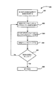
図1は、本発明に従うエピタキシャル膜を形成する第1の例示的な方法のフローチャートである。図1を参照すると、ステップ101において、基板は、処理チャンバ内にロードされ、約800℃未満の温度まで加熱される。一部の実施形態において、エピタキシャル膜形成中に用いられる低温範囲は、例えば、750℃未満、700℃未満、650℃未満である。
FIG. 1 is a flowchart of a first exemplary method of forming an epitaxial film according to the present invention. Referring to FIG. 1, in
ステップ102において、基板キャリアガス及び/又はドーパントと共にシランおよびジクロロシランが処理チャンバ内に流され、基板上にエピタキシャル膜を形成する。一部の実施形態において、例えばHCl、Cl2、HCl及びCl2の混合等のような1以上のエッチャントガスは、シリコン源ガスと同時に(例えば、同時の堆積・エッチング処理中に)流されてもよい。他の実施形態において、別個のエッチャントステップが、堆積処理に続いて(例えば、AGS処理中に)使用されてもよい。
In
所望のエピタキシャル膜厚が達成されるまで、堆積とエッチングが続けられる。一部の実施形態において、1より大きいSiH4とDCSの比(SiH4:DCS)、例えば、2:1,3:1,4:1,5:1,7:1,10:1等が使用されてもよい。他のシリコン源の比が用いられてもよい。 Deposition and etching are continued until the desired epitaxial film thickness is achieved. In some embodiments, a ratio of SiH 4 to DCS greater than 1 (SiH 4 : DCS), such as 2: 1, 3: 1, 4: 1, 5: 1, 7: 1, 10: 1, etc. May be used. Other silicon source ratios may be used.
図2は、本発明に従うエピタキシャル膜を形成する第2の例示的方法200のフローチャートである。図2を参照すると、ステップ201において、基板は、処理チャンバ内にロードされ、約800℃以下の温度まで加熱される。一部の実施形態では、低い温度範囲(750℃未満、700℃未満、650℃未満など)がエピタキシャル膜形成中に用いられてもよい。
FIG. 2 is a flowchart of a second
ステップ202では、シランとジクロロシランが、適したキャリアガス及び/又はドーパントと共に処理チャンバ内に流され、基板上にエピタキシャル膜を形成する。一部の実施形態では、約10sccmから約100sccmのシランが使用されるが、約10sccmから約100sccmのジクロロシランが使用されてもよい。約5Torrから約50Torrの範囲の圧力が使用されてもよい。堆積は、約2秒から250秒の間で実施されてもよいが、好ましくは、約5秒から10秒である。一部の実施形態では、1より大きいSiH4とDCSの比(SiH4:DCS)、例えば、2:1,3:1,4:1,5:1,7:1,10:1等が使用されてもよい。他の流量、圧力、温度、時間及び/又はSiH4:DCSの比が用いられてもよい。
In
ステップ203では、エッチャントガス(例えば、HCl及び/又はCl2)が、適したキャリアガスと共に処理チャンバ内に流され、ステップ202の間、堆積された材料をエッチングする。例えば、基板は、エッチャントとして約50sccmから約500sccmの塩化水素(HCl)、約5Torrから約100Torrのチャンバ圧力を用いて、約2秒から250秒、より好ましくは約5秒から10秒の間、エッチングされてもよい。他のエッチャント、流量、圧力および/または時間が用いられてもよい。
In
ステップ204では、エッチングサイクルの後、パージサイクルが約2秒から250秒、好ましくは約5秒から10秒の間、行われてもよい。他のパージ時間が用いられてもよい。
In
ステップ205では、所望のエピタキシャル膜厚が達成されたかが決定される。達成されたのであれば、処理はステップ206で終了する。そうでなければ、処理は、ステップ202に戻り、追加のエピタキシャル材料を基板に堆積する。
In
前述した説明は、本発明の単なる例示的な実施形態を開示するものである。本発明の範囲に該当する前述された装置および方法の変形例は、当該技術分野の当業者にとって明らかであろう。例えば、低い温度範囲(750℃未満、700℃未満、650℃未満など)は、エピタキシャル膜の形成中に用いられてもよい。 The foregoing description discloses merely exemplary embodiments of the invention. Variations of the above-described apparatus and methods falling within the scope of the invention will be apparent to those skilled in the art. For example, low temperature ranges (less than 750 ° C., less than 700 ° C., less than 650 ° C., etc.) may be used during the formation of the epitaxial film.
したがって、本発明は、その例示的な実施形態との関係で開示されているが、添付された請求項に規定されているように、他の実施形態が本発明の精神及び範囲に該当することは言うまでもない。 Accordingly, while the invention has been disclosed in connection with exemplary embodiments thereof, other embodiments fall within the spirit and scope of the invention as defined in the appended claims. Needless to say.
Claims (13)
シリコン基板を準備するステップと、
650℃以上800℃未満の温度まで前記基板を加熱し、選択的エピタキシャル膜形成処理を前記基板上で行い、前記選択的エピタキシャル膜形成処理中に、シリコン源としてシランおよびジクロロシランの両方を使用することにより、前記エピタキシャル層を形成するステップと、
を備え、
前記選択的エピタキシャル膜形成処理を行うステップは、その後にエッチングステップが続く堆積ステップを行う工程を備え、
前記堆積ステップを行う工程は、シラン流とジクロロシラン流を与えることを含み、
前記堆積ステップを行う工程は、10秒までの間、シランおよびジクロロシランを流すことを含む、前記方法。In a method of forming an epitaxial layer,
Preparing a silicon substrate;
The substrate is heated to a temperature of 650 ° C. or higher and lower than 800 ° C., and a selective epitaxial film forming process is performed on the substrate, and both silane and dichlorosilane are used as a silicon source during the selective epitaxial film forming process. Forming the epitaxial layer;
With
The step of performing the selective epitaxial film forming process includes a step of performing a deposition step followed by an etching step,
Performing the deposition step includes providing a silane stream and a dichlorosilane stream;
The method, wherein the step of performing the deposition step comprises flowing silane and dichlorosilane for up to 10 seconds.
シランおよびジクロロシランを流す工程、
塩化水素(HCl)および塩素(Cl2)のうち少なくとも1つを含むエッチングガスを流す工程、を備える、請求項1に記載の方法。Performing the selective epitaxial film forming process,
Flowing silane and dichlorosilane;
The method according to claim 1, further comprising flowing an etching gas containing at least one of hydrogen chloride (HCl) and chlorine (Cl 2 ).
シリコン基板を準備するステップと、
650℃以上800℃未満の温度まで前記基板を加熱し、少なくとも1つの堆積工程と、少なくとも1つのエッチング工程とを備える選択的エピタキシャル膜形成処理を行うステップであって、
少なくとも1つの前記堆積工程は、その後に少なくとも1つの前記エッチング工程が続き、
前記堆積工程と前記エッチング工程は交互で行われ、
前記堆積工程は、それぞれ10から100sccmの流量、5から50Torrの堆積圧力で、シランとジクロロシランを流すことを含み、
前記エッチング工程は、10秒までの間、塩化水素と塩素のうち少なくとも1つを流すことを含む、前記ステップと、
を備える、前記方法。In a method of forming an epitaxial layer,
Preparing a silicon substrate;
To a temperature below 650 ° C. or higher 800 ° C. by heating the substrate, at least one deposition step, a step of performing selective epitaxial film forming process and at least one etching process,
At least one of the deposition steps followed by at least one of the etching steps;
The deposition step and the etching step are performed alternately,
The deposition step includes flowing silane and dichlorosilane at a flow rate of 10 to 100 sccm, respectively, and a deposition pressure of 5 to 50 Torr;
The etching step includes flowing at least one of hydrogen chloride and chlorine for up to 10 seconds;
Said method.
シリコン基板を準備するステップと、
650℃以上800℃未満の温度まで前記基板を加熱し、選択的エピタキシャル膜形成処理を前記基板上で行い、前記選択的エピタキシャル膜形成処理中に、シリコン源としてシランおよびジクロロシランの両方を使用することにより、前記エピタキシャル層を形成するステップと、
を備え、
前記選択的エピタキシャル膜形成処理を行うステップは、その後にエッチングステップが続く堆積ステップを行う工程を備え、
前記堆積ステップを行う工程は、10秒までの間、シランおよびジクロロシランを流すことを含み、
ジクロロシランに対するシランの比が1より大きい、前記方法。In a method of forming an epitaxial layer,
Preparing a silicon substrate;
The substrate is heated to a temperature of 650 ° C. or higher and lower than 800 ° C., and a selective epitaxial film forming process is performed on the substrate, and both silane and dichlorosilane are used as a silicon source during the selective epitaxial film forming process. Forming the epitaxial layer;
With
The step of performing the selective epitaxial film forming process includes a step of performing a deposition step followed by an etching step,
Performing the deposition step comprises flowing silane and dichlorosilane for up to 10 seconds;
The method, wherein the ratio of silane to dichlorosilane is greater than 1.
Applications Claiming Priority (3)
| Application Number | Priority Date | Filing Date | Title |
|---|---|---|---|
| US82095606P | 2006-07-31 | 2006-07-31 | |
| US60/820,956 | 2006-07-31 | ||
| PCT/US2007/017053 WO2008033186A1 (en) | 2006-07-31 | 2007-07-30 | Methods of controlling morphology during epitaxial layer formation |
Publications (3)
| Publication Number | Publication Date |
|---|---|
| JP2009545884A JP2009545884A (en) | 2009-12-24 |
| JP2009545884A5 JP2009545884A5 (en) | 2010-09-02 |
| JP5175285B2 true JP5175285B2 (en) | 2013-04-03 |
Family
ID=39184089
Family Applications (1)
| Application Number | Title | Priority Date | Filing Date |
|---|---|---|---|
| JP2009522826A Expired - Fee Related JP5175285B2 (en) | 2006-07-31 | 2007-07-30 | Method for controlling morphology during epitaxial layer formation |
Country Status (7)
| Country | Link |
|---|---|
| US (1) | US7588980B2 (en) |
| JP (1) | JP5175285B2 (en) |
| KR (1) | KR101369355B1 (en) |
| CN (1) | CN101496150B (en) |
| DE (1) | DE112007001813T5 (en) |
| TW (1) | TWI390606B (en) |
| WO (1) | WO2008033186A1 (en) |
Families Citing this family (18)
| Publication number | Priority date | Publication date | Assignee | Title |
|---|---|---|---|---|
| US20100120235A1 (en) * | 2008-11-13 | 2010-05-13 | Applied Materials, Inc. | Methods for forming silicon germanium layers |
| US8501594B2 (en) * | 2003-10-10 | 2013-08-06 | Applied Materials, Inc. | Methods for forming silicon germanium layers |
| US7682940B2 (en) | 2004-12-01 | 2010-03-23 | Applied Materials, Inc. | Use of Cl2 and/or HCl during silicon epitaxial film formation |
| JP2009512196A (en) * | 2005-10-05 | 2009-03-19 | アプライド マテリアルズ インコーポレイテッド | Method and apparatus for epitaxial film formation |
| WO2007112058A2 (en) * | 2006-03-24 | 2007-10-04 | Applied Materials, Inc. | Carbon precursors for use during silicon epitaxial firm formation |
| WO2007117583A2 (en) * | 2006-04-07 | 2007-10-18 | Applied Materials Inc. | Cluster tool for epitaxial film formation |
| US7674337B2 (en) * | 2006-04-07 | 2010-03-09 | Applied Materials, Inc. | Gas manifolds for use during epitaxial film formation |
| US8029620B2 (en) | 2006-07-31 | 2011-10-04 | Applied Materials, Inc. | Methods of forming carbon-containing silicon epitaxial layers |
| US7897495B2 (en) * | 2006-12-12 | 2011-03-01 | Applied Materials, Inc. | Formation of epitaxial layer containing silicon and carbon |
| US9064960B2 (en) * | 2007-01-31 | 2015-06-23 | Applied Materials, Inc. | Selective epitaxy process control |
| JP4635062B2 (en) | 2008-03-11 | 2011-02-16 | 株式会社東芝 | Manufacturing method of semiconductor device |
| KR101776926B1 (en) | 2010-09-07 | 2017-09-08 | 삼성전자주식회사 | Semiconductor device and method for manufacturing the same |
| CN103779278A (en) * | 2012-10-22 | 2014-05-07 | 中芯国际集成电路制造(上海)有限公司 | CMOS (Complementary Metal Oxide Semiconductor) tube forming method |
| JP5931780B2 (en) * | 2013-03-06 | 2016-06-08 | 東京エレクトロン株式会社 | Selective epitaxial growth method and film forming apparatus |
| KR102422158B1 (en) | 2015-12-23 | 2022-07-20 | 에스케이하이닉스 주식회사 | Semiconductor device and method for manufacturing the same |
| JP6640596B2 (en) * | 2016-02-22 | 2020-02-05 | 東京エレクトロン株式会社 | Film formation method |
| US10446393B2 (en) * | 2017-05-08 | 2019-10-15 | Asm Ip Holding B.V. | Methods for forming silicon-containing epitaxial layers and related semiconductor device structures |
| JP6489198B1 (en) * | 2017-12-25 | 2019-03-27 | 株式会社Sumco | Method for evaluating contamination of epitaxial wafer and method for manufacturing epitaxial wafer using the method |
Family Cites Families (127)
| Publication number | Priority date | Publication date | Assignee | Title |
|---|---|---|---|---|
| US3675619A (en) | 1969-02-25 | 1972-07-11 | Monsanto Co | Apparatus for production of epitaxial films |
| NL187942C (en) | 1980-08-18 | 1992-02-17 | Philips Nv | ZENERDIODE AND METHOD OF MANUFACTURE THEREOF |
| US5294286A (en) | 1984-07-26 | 1994-03-15 | Research Development Corporation Of Japan | Process for forming a thin film of silicon |
| US5693139A (en) | 1984-07-26 | 1997-12-02 | Research Development Corporation Of Japan | Growth of doped semiconductor monolayers |
| JPH0639357B2 (en) | 1986-09-08 | 1994-05-25 | 新技術開発事業団 | Method for growing element semiconductor single crystal thin film |
| US5607511A (en) | 1992-02-21 | 1997-03-04 | International Business Machines Corporation | Method and apparatus for low temperature, low pressure chemical vapor deposition of epitaxial silicon layers |
| US5112439A (en) | 1988-11-30 | 1992-05-12 | Mcnc | Method for selectively depositing material on substrates |
| JPH0824191B2 (en) | 1989-03-17 | 1996-03-06 | 富士通株式会社 | Thin film transistor |
| EP0413982B1 (en) | 1989-07-27 | 1997-05-14 | Junichi Nishizawa | Impurity doping method with adsorbed diffusion source |
| JP2880322B2 (en) | 1991-05-24 | 1999-04-05 | キヤノン株式会社 | Method of forming deposited film |
| US5227330A (en) * | 1991-10-31 | 1993-07-13 | International Business Machines Corporation | Comprehensive process for low temperature SI epit axial growth |
| US5480818A (en) | 1992-02-10 | 1996-01-02 | Fujitsu Limited | Method for forming a film and method for manufacturing a thin film transistor |
| JP2917694B2 (en) | 1992-04-02 | 1999-07-12 | 日本電気株式会社 | Compound semiconductor vapor deposition method and apparatus therefor |
| JPH0750690B2 (en) | 1992-08-21 | 1995-05-31 | 日本電気株式会社 | Method and apparatus for epitaxial growth of semiconductor crystal using halide |
| US5273930A (en) | 1992-09-03 | 1993-12-28 | Motorola, Inc. | Method of forming a non-selective silicon-germanium epitaxial film |
| US5236545A (en) | 1992-10-05 | 1993-08-17 | The Board Of Governors Of Wayne State University | Method for heteroepitaxial diamond film development |
| JP3255469B2 (en) | 1992-11-30 | 2002-02-12 | 三菱電機株式会社 | Laser thin film forming equipment |
| JP3265042B2 (en) | 1993-03-18 | 2002-03-11 | 東京エレクトロン株式会社 | Film formation method |
| JPH0729897A (en) | 1993-06-25 | 1995-01-31 | Nec Corp | Manufacture of semiconductor device |
| US5372860A (en) | 1993-07-06 | 1994-12-13 | Corning Incorporated | Silicon device production |
| JPH07109573A (en) | 1993-10-12 | 1995-04-25 | Semiconductor Energy Lab Co Ltd | Glass substrate and heat treatment |
| US5796116A (en) | 1994-07-27 | 1998-08-18 | Sharp Kabushiki Kaisha | Thin-film semiconductor device including a semiconductor film with high field-effect mobility |
| US6342277B1 (en) | 1996-08-16 | 2002-01-29 | Licensee For Microelectronics: Asm America, Inc. | Sequential chemical vapor deposition |
| US5916365A (en) | 1996-08-16 | 1999-06-29 | Sherman; Arthur | Sequential chemical vapor deposition |
| US5807792A (en) | 1996-12-18 | 1998-09-15 | Siemens Aktiengesellschaft | Uniform distribution of reactants in a device layer |
| US6335280B1 (en) | 1997-01-13 | 2002-01-01 | Asm America, Inc. | Tungsten silicide deposition process |
| US6055927A (en) | 1997-01-14 | 2000-05-02 | Applied Komatsu Technology, Inc. | Apparatus and method for white powder reduction in silicon nitride deposition using remote plasma source cleaning technology |
| US5849092A (en) | 1997-02-25 | 1998-12-15 | Applied Materials, Inc. | Process for chlorine trifluoride chamber cleaning |
| TW417249B (en) | 1997-05-14 | 2001-01-01 | Applied Materials Inc | Reliability barrier integration for cu application |
| US6118216A (en) | 1997-06-02 | 2000-09-12 | Osram Sylvania Inc. | Lead and arsenic free borosilicate glass and lamp containing same |
| KR100385946B1 (en) | 1999-12-08 | 2003-06-02 | 삼성전자주식회사 | Method for forming a metal layer by an atomic layer deposition and a semiconductor device with the metal layer as a barrier metal layer, an upper electrode, or a lower electrode of capacitor |
| US6287965B1 (en) | 1997-07-28 | 2001-09-11 | Samsung Electronics Co, Ltd. | Method of forming metal layer using atomic layer deposition and semiconductor device having the metal layer as barrier metal layer or upper or lower electrode of capacitor |
| KR100269306B1 (en) | 1997-07-31 | 2000-10-16 | 윤종용 | Integrate circuit device having buffer layer containing metal oxide stabilized by low temperature treatment and fabricating method thereof |
| KR100261017B1 (en) | 1997-08-19 | 2000-08-01 | 윤종용 | Method for forming metal wiring of semiconductor device |
| US6042654A (en) | 1998-01-13 | 2000-03-28 | Applied Materials, Inc. | Method of cleaning CVD cold-wall chamber and exhaust lines |
| US6383955B1 (en) | 1998-02-05 | 2002-05-07 | Asm Japan K.K. | Silicone polymer insulation film on semiconductor substrate and method for forming the film |
| TW437017B (en) | 1998-02-05 | 2001-05-28 | Asm Japan Kk | Silicone polymer insulation film on semiconductor substrate and method for formation thereof |
| US6514880B2 (en) | 1998-02-05 | 2003-02-04 | Asm Japan K.K. | Siloxan polymer film on semiconductor substrate and method for forming same |
| US6159852A (en) | 1998-02-13 | 2000-12-12 | Micron Technology, Inc. | Method of depositing polysilicon, method of fabricating a field effect transistor, method of forming a contact to a substrate, method of forming a capacitor |
| US6797558B2 (en) | 2001-04-24 | 2004-09-28 | Micron Technology, Inc. | Methods of forming a capacitor with substantially selective deposite of polysilicon on a substantially crystalline capacitor dielectric layer |
| WO1999045167A1 (en) | 1998-03-06 | 1999-09-10 | Asm America, Inc. | Method of depositing silicon with high step coverage |
| US6019839A (en) * | 1998-04-17 | 2000-02-01 | Applied Materials, Inc. | Method and apparatus for forming an epitaxial titanium silicide film by low pressure chemical vapor deposition |
| JP4214585B2 (en) | 1998-04-24 | 2009-01-28 | 富士ゼロックス株式会社 | Semiconductor device, semiconductor device manufacturing method and manufacturing apparatus |
| US6025627A (en) | 1998-05-29 | 2000-02-15 | Micron Technology, Inc. | Alternate method and structure for improved floating gate tunneling devices |
| FR2779572B1 (en) | 1998-06-05 | 2003-10-17 | St Microelectronics Sa | LOW NOISE VERTICAL BIPOLAR TRANSISTOR AND MANUFACTURING METHOD THEREOF |
| KR100275738B1 (en) | 1998-08-07 | 2000-12-15 | 윤종용 | Method for producing thin film using atomatic layer deposition |
| JP4204671B2 (en) | 1998-09-11 | 2009-01-07 | 三菱電機株式会社 | Manufacturing method of semiconductor device |
| KR100287180B1 (en) | 1998-09-17 | 2001-04-16 | 윤종용 | Method for manufacturing semiconductor device including metal interconnection formed using interface control layer |
| KR100327328B1 (en) | 1998-10-13 | 2002-05-09 | 윤종용 | Method for forming dielectric layer of capacitor having partially different thickness in the layer |
| US6200893B1 (en) | 1999-03-11 | 2001-03-13 | Genus, Inc | Radical-assisted sequential CVD |
| US6305314B1 (en) | 1999-03-11 | 2001-10-23 | Genvs, Inc. | Apparatus and concept for minimizing parasitic chemical vapor deposition during atomic layer deposition |
| US6653212B1 (en) | 1999-04-20 | 2003-11-25 | Sony Corporation | Method and apparatus for thin-film deposition, and method of manufacturing thin-film semiconductor device |
| US6124158A (en) | 1999-06-08 | 2000-09-26 | Lucent Technologies Inc. | Method of reducing carbon contamination of a thin dielectric film by using gaseous organic precursors, inert gas, and ozone to react with carbon contaminants |
| US6391785B1 (en) | 1999-08-24 | 2002-05-21 | Interuniversitair Microelektronica Centrum (Imec) | Method for bottomless deposition of barrier layers in integrated circuit metallization schemes |
| US6511539B1 (en) * | 1999-09-08 | 2003-01-28 | Asm America, Inc. | Apparatus and method for growth of a thin film |
| US6489241B1 (en) | 1999-09-17 | 2002-12-03 | Applied Materials, Inc. | Apparatus and method for surface finishing a silicon film |
| FI117942B (en) | 1999-10-14 | 2007-04-30 | Asm Int | Process for making oxide thin films |
| FR2801420B1 (en) | 1999-11-23 | 2002-04-12 | St Microelectronics Sa | LOW FREQUENCY LOW NOISE VERTICAL BIPOLAR TRANSISTOR AND HIGH CURRENT GAIN, AND MANUFACTURING METHOD THEREOF |
| US6780704B1 (en) | 1999-12-03 | 2004-08-24 | Asm International Nv | Conformal thin films over textured capacitor electrodes |
| US6291319B1 (en) | 1999-12-17 | 2001-09-18 | Motorola, Inc. | Method for fabricating a semiconductor structure having a stable crystalline interface with silicon |
| US6348420B1 (en) | 1999-12-23 | 2002-02-19 | Asm America, Inc. | Situ dielectric stacks |
| EP1123991A3 (en) | 2000-02-08 | 2002-11-13 | Asm Japan K.K. | Low dielectric constant materials and processes |
| US6492283B2 (en) | 2000-02-22 | 2002-12-10 | Asm Microchemistry Oy | Method of forming ultrathin oxide layer |
| KR100803770B1 (en) * | 2000-03-07 | 2008-02-15 | 에이에스엠 인터내셔널 엔.브이. | Graded thin films |
| KR100363088B1 (en) | 2000-04-20 | 2002-12-02 | 삼성전자 주식회사 | Method of manufacturing barrier metal layer using atomic layer deposition method |
| US6458718B1 (en) | 2000-04-28 | 2002-10-01 | Asm Japan K.K. | Fluorine-containing materials and processes |
| US6630413B2 (en) | 2000-04-28 | 2003-10-07 | Asm Japan K.K. | CVD syntheses of silicon nitride materials |
| EP2293322A1 (en) * | 2000-06-08 | 2011-03-09 | Genitech, Inc. | Method for forming a metal nitride layer |
| JP3650727B2 (en) * | 2000-08-10 | 2005-05-25 | Hoya株式会社 | Silicon carbide manufacturing method |
| KR100373853B1 (en) | 2000-08-11 | 2003-02-26 | 삼성전자주식회사 | Selective epitaxial growth method in semiconductor device |
| US6461909B1 (en) | 2000-08-30 | 2002-10-08 | Micron Technology, Inc. | Process for fabricating RuSixOy-containing adhesion layers |
| JP5290488B2 (en) * | 2000-09-28 | 2013-09-18 | プレジデント アンド フェロウズ オブ ハーバード カレッジ | Vapor growth of oxides, silicates and phosphates |
| KR100378186B1 (en) | 2000-10-19 | 2003-03-29 | 삼성전자주식회사 | Semiconductor device adopting thin film formed by atomic layer deposition and fabrication method thereof |
| US6613695B2 (en) * | 2000-11-24 | 2003-09-02 | Asm America, Inc. | Surface preparation prior to deposition |
| JP4333900B2 (en) | 2000-11-30 | 2009-09-16 | エーエスエム インターナショナル エヌ.ヴェー. | Magnetic memory cell, method for manufacturing magnetic structure and magnetic element, and method for growing metal layer for magnetic structure |
| KR100385947B1 (en) | 2000-12-06 | 2003-06-02 | 삼성전자주식회사 | Method of forming thin film by atomic layer deposition |
| KR20020049875A (en) | 2000-12-20 | 2002-06-26 | 윤종용 | Ferroelectric capacitor in semiconductor memory device and method for manufacturing the same |
| KR100393208B1 (en) | 2001-01-15 | 2003-07-31 | 삼성전자주식회사 | Semiconductor device using doped polycrystalline silicon-germanium layer and method for manufacturing the same |
| US6426265B1 (en) * | 2001-01-30 | 2002-07-30 | International Business Machines Corporation | Incorporation of carbon in silicon/silicon germanium epitaxial layer to enhance yield for Si-Ge bipolar technology |
| KR101027485B1 (en) * | 2001-02-12 | 2011-04-06 | 에이에스엠 아메리카, 인코포레이티드 | Improved process for deposition of semiconductor films |
| US20020117399A1 (en) * | 2001-02-23 | 2002-08-29 | Applied Materials, Inc. | Atomically thin highly resistive barrier layer in a copper via |
| US6576535B2 (en) | 2001-04-11 | 2003-06-10 | Texas Instruments Incorporated | Carbon doped epitaxial layer for high speed CB-CMOS |
| US7108748B2 (en) * | 2001-05-30 | 2006-09-19 | Asm America, Inc. | Low temperature load and bake |
| US6828218B2 (en) * | 2001-05-31 | 2004-12-07 | Samsung Electronics Co., Ltd. | Method of forming a thin film using atomic layer deposition |
| US6391803B1 (en) | 2001-06-20 | 2002-05-21 | Samsung Electronics Co., Ltd. | Method of forming silicon containing thin films by atomic layer deposition utilizing trisdimethylaminosilane |
| US6861334B2 (en) * | 2001-06-21 | 2005-03-01 | Asm International, N.V. | Method of fabricating trench isolation structures for integrated circuits using atomic layer deposition |
| US6806145B2 (en) * | 2001-08-31 | 2004-10-19 | Asm International, N.V. | Low temperature method of forming a gate stack with a high k layer deposited over an interfacial oxide layer |
| US6960537B2 (en) * | 2001-10-02 | 2005-11-01 | Asm America, Inc. | Incorporation of nitrogen into high k dielectric film |
| US20030072884A1 (en) * | 2001-10-15 | 2003-04-17 | Applied Materials, Inc. | Method of titanium and titanium nitride layer deposition |
| US6916398B2 (en) * | 2001-10-26 | 2005-07-12 | Applied Materials, Inc. | Gas delivery apparatus and method for atomic layer deposition |
| KR20030035152A (en) | 2001-10-30 | 2003-05-09 | 주식회사 하이닉스반도체 | Method for fabricating semiconductor wafer |
| US6743681B2 (en) * | 2001-11-09 | 2004-06-01 | Micron Technology, Inc. | Methods of Fabricating Gate and Storage Dielectric Stacks having Silicon-Rich-Nitride |
| US6590344B2 (en) | 2001-11-20 | 2003-07-08 | Taiwan Semiconductor Manufacturing Co., Ltd. | Selectively controllable gas feed zones for a plasma reactor |
| US6773507B2 (en) * | 2001-12-06 | 2004-08-10 | Applied Materials, Inc. | Apparatus and method for fast-cycle atomic layer deposition |
| US7081271B2 (en) * | 2001-12-07 | 2006-07-25 | Applied Materials, Inc. | Cyclical deposition of refractory metal silicon nitride |
| US6696332B2 (en) * | 2001-12-26 | 2004-02-24 | Texas Instruments Incorporated | Bilayer deposition to avoid unwanted interfacial reactions during high K gate dielectric processing |
| US6620670B2 (en) | 2002-01-18 | 2003-09-16 | Applied Materials, Inc. | Process conditions and precursors for atomic layer deposition (ALD) of AL2O3 |
| US6911391B2 (en) * | 2002-01-26 | 2005-06-28 | Applied Materials, Inc. | Integration of titanium and titanium nitride layers |
| JP3914064B2 (en) * | 2002-02-28 | 2007-05-16 | 富士通株式会社 | Method and apparatus for growing mixed crystal film |
| US7105891B2 (en) * | 2002-07-15 | 2006-09-12 | Texas Instruments Incorporated | Gate structure and method |
| US6723658B2 (en) * | 2002-07-15 | 2004-04-20 | Texas Instruments Incorporated | Gate structure and method |
| US7449385B2 (en) * | 2002-07-26 | 2008-11-11 | Texas Instruments Incorporated | Gate dielectric and method |
| US6919251B2 (en) * | 2002-07-31 | 2005-07-19 | Texas Instruments Incorporated | Gate dielectric and method |
| US7186630B2 (en) * | 2002-08-14 | 2007-03-06 | Asm America, Inc. | Deposition of amorphous silicon-containing films |
| KR100542736B1 (en) * | 2002-08-17 | 2006-01-11 | 삼성전자주식회사 | Method of forming oxide layer using atomic layer deposition method and method of forming capacitor of semiconductor device using the same |
| US7199023B2 (en) * | 2002-08-28 | 2007-04-03 | Micron Technology, Inc. | Atomic layer deposited HfSiON dielectric films wherein each precursor is independendently pulsed |
| US6759286B2 (en) * | 2002-09-16 | 2004-07-06 | Ajay Kumar | Method of fabricating a gate structure of a field effect transistor using a hard mask |
| US6998305B2 (en) | 2003-01-24 | 2006-02-14 | Asm America, Inc. | Enhanced selectivity for epitaxial deposition |
| JP3872027B2 (en) | 2003-03-07 | 2007-01-24 | 株式会社東芝 | Cleaning method and semiconductor manufacturing apparatus |
| KR20050119662A (en) * | 2003-03-28 | 2005-12-21 | 코닌클리즈케 필립스 일렉트로닉스 엔.브이. | Method of epitaxial deposition of an n-doped silicon layer |
| JP4224492B2 (en) | 2003-06-09 | 2009-02-12 | シーケーディ株式会社 | Pressure control system and flow rate control system |
| JP2005167064A (en) | 2003-12-04 | 2005-06-23 | Sharp Corp | Nonvolatile semiconductor storage device |
| US7045432B2 (en) * | 2004-02-04 | 2006-05-16 | Freescale Semiconductor, Inc. | Method for forming a semiconductor device with local semiconductor-on-insulator (SOI) |
| US7071117B2 (en) * | 2004-02-27 | 2006-07-04 | Micron Technology, Inc. | Semiconductor devices and methods for depositing a dielectric film |
| US7230274B2 (en) | 2004-03-01 | 2007-06-12 | Cree, Inc | Reduction of carrot defects in silicon carbide epitaxy |
| KR100532509B1 (en) | 2004-03-26 | 2005-11-30 | 삼성전자주식회사 | Trench capacitor using SiGe layer and method of fabricating the same |
| US7396743B2 (en) * | 2004-06-10 | 2008-07-08 | Singh Kaushal K | Low temperature epitaxial growth of silicon-containing films using UV radiation |
| US7361563B2 (en) | 2004-06-17 | 2008-04-22 | Samsung Electronics Co., Ltd. | Methods of fabricating a semiconductor device using a selective epitaxial growth technique |
| KR100607409B1 (en) * | 2004-08-23 | 2006-08-02 | 삼성전자주식회사 | Method for etching substrate and method for menufacturing semiconductor device using the same |
| US7312128B2 (en) | 2004-12-01 | 2007-12-25 | Applied Materials, Inc. | Selective epitaxy process with alternating gas supply |
| US7682940B2 (en) * | 2004-12-01 | 2010-03-23 | Applied Materials, Inc. | Use of Cl2 and/or HCl during silicon epitaxial film formation |
| US7560352B2 (en) * | 2004-12-01 | 2009-07-14 | Applied Materials, Inc. | Selective deposition |
| US7235492B2 (en) * | 2005-01-31 | 2007-06-26 | Applied Materials, Inc. | Low temperature etchant for treatment of silicon-containing surfaces |
| US7687383B2 (en) * | 2005-02-04 | 2010-03-30 | Asm America, Inc. | Methods of depositing electrically active doped crystalline Si-containing films |
| JP2009512196A (en) * | 2005-10-05 | 2009-03-19 | アプライド マテリアルズ インコーポレイテッド | Method and apparatus for epitaxial film formation |
| WO2007112058A2 (en) * | 2006-03-24 | 2007-10-04 | Applied Materials, Inc. | Carbon precursors for use during silicon epitaxial firm formation |
| US8029620B2 (en) * | 2006-07-31 | 2011-10-04 | Applied Materials, Inc. | Methods of forming carbon-containing silicon epitaxial layers |
-
2007
- 2007-07-30 KR KR1020097003879A patent/KR101369355B1/en active IP Right Grant
- 2007-07-30 WO PCT/US2007/017053 patent/WO2008033186A1/en active Application Filing
- 2007-07-30 CN CN2007800284868A patent/CN101496150B/en active Active
- 2007-07-30 DE DE112007001813T patent/DE112007001813T5/en not_active Withdrawn
- 2007-07-30 JP JP2009522826A patent/JP5175285B2/en not_active Expired - Fee Related
- 2007-07-30 US US11/830,830 patent/US7588980B2/en active Active
- 2007-07-31 TW TW096128088A patent/TWI390606B/en not_active IP Right Cessation
Also Published As
| Publication number | Publication date |
|---|---|
| WO2008033186A1 (en) | 2008-03-20 |
| DE112007001813T5 (en) | 2009-07-09 |
| US20080026549A1 (en) | 2008-01-31 |
| US7588980B2 (en) | 2009-09-15 |
| CN101496150A (en) | 2009-07-29 |
| CN101496150B (en) | 2012-07-18 |
| KR101369355B1 (en) | 2014-03-04 |
| JP2009545884A (en) | 2009-12-24 |
| TWI390606B (en) | 2013-03-21 |
| TW200816280A (en) | 2008-04-01 |
| KR20090037481A (en) | 2009-04-15 |
Similar Documents
| Publication | Publication Date | Title |
|---|---|---|
| JP5175285B2 (en) | Method for controlling morphology during epitaxial layer formation | |
| JP5090451B2 (en) | Method for forming carbon-containing silicon epitaxial layer | |
| TWI613705B (en) | Method to grow thin epitaxial films at low temperature | |
| TWI419204B (en) | Selective deposition | |
| CN101069264B (en) | Selective epitaxy technique with alternating gas supply | |
| KR101074186B1 (en) | Cluster tool for epitaxial film formation | |
| TWI741121B (en) | Method and apparatus for selective epitaxy | |
| TWI512792B (en) | Selective epitaxy process control | |
| JP2005536054A (en) | Deposition of amorphous silicon-containing films | |
| JP2007535147A (en) | In situ doped epitaxial film | |
| KR100434698B1 (en) | Method for growing epitaxial layer in semiconductor device | |
| US7253085B2 (en) | Deposition methods | |
| TWI738207B (en) | Methods and apparatus for metal silicide deposition | |
| TWI774716B (en) | Method for manufacturing a semiconductor device | |
| US20180166288A1 (en) | Methods for silicide formation | |
| US9012328B2 (en) | Carbon addition for low resistivity in situ doped silicon epitaxy | |
| US8551871B2 (en) | Method of fabricating semiconductor device | |
| CN117711926A (en) | Method for selectively forming Si-containing epitaxial layer on substrate |
Legal Events
| Date | Code | Title | Description |
|---|---|---|---|
| A521 | Written amendment |
Free format text: JAPANESE INTERMEDIATE CODE: A523 Effective date: 20100716 |
|
| A621 | Written request for application examination |
Free format text: JAPANESE INTERMEDIATE CODE: A621 Effective date: 20100716 |
|
| RD03 | Notification of appointment of power of attorney |
Free format text: JAPANESE INTERMEDIATE CODE: A7423 Effective date: 20101130 |
|
| RD04 | Notification of resignation of power of attorney |
Free format text: JAPANESE INTERMEDIATE CODE: A7424 Effective date: 20101210 |
|
| A977 | Report on retrieval |
Free format text: JAPANESE INTERMEDIATE CODE: A971007 Effective date: 20120302 |
|
| A131 | Notification of reasons for refusal |
Free format text: JAPANESE INTERMEDIATE CODE: A131 Effective date: 20120327 |
|
| A521 | Written amendment |
Free format text: JAPANESE INTERMEDIATE CODE: A523 Effective date: 20120626 |
|
| A131 | Notification of reasons for refusal |
Free format text: JAPANESE INTERMEDIATE CODE: A131 Effective date: 20120731 |
|
| RD04 | Notification of resignation of power of attorney |
Free format text: JAPANESE INTERMEDIATE CODE: A7424 Effective date: 20120925 |
|
| A601 | Written request for extension of time |
Free format text: JAPANESE INTERMEDIATE CODE: A601 Effective date: 20121030 |
|
| A602 | Written permission of extension of time |
Free format text: JAPANESE INTERMEDIATE CODE: A602 Effective date: 20121106 |
|
| A521 | Written amendment |
Free format text: JAPANESE INTERMEDIATE CODE: A523 Effective date: 20121107 |
|
| A01 | Written decision to grant a patent or to grant a registration (utility model) |
Free format text: JAPANESE INTERMEDIATE CODE: A01 Effective date: 20121204 |
|
| A61 | First payment of annual fees (during grant procedure) |
Free format text: JAPANESE INTERMEDIATE CODE: A61 Effective date: 20130104 |
|
| LAPS | Cancellation because of no payment of annual fees |