JP5174246B2 - Adder - Google Patents
Adder Download PDFInfo
- Publication number
- JP5174246B2 JP5174246B2 JP2011531714A JP2011531714A JP5174246B2 JP 5174246 B2 JP5174246 B2 JP 5174246B2 JP 2011531714 A JP2011531714 A JP 2011531714A JP 2011531714 A JP2011531714 A JP 2011531714A JP 5174246 B2 JP5174246 B2 JP 5174246B2
- Authority
- JP
- Japan
- Prior art keywords
- wave
- input
- calculator
- unit
- output
- Prior art date
- Legal status (The legal status is an assumption and is not a legal conclusion. Google has not performed a legal analysis and makes no representation as to the accuracy of the status listed.)
- Expired - Fee Related
Links
Images


Classifications
-
- G—PHYSICS
- G06—COMPUTING; CALCULATING OR COUNTING
- G06F—ELECTRIC DIGITAL DATA PROCESSING
- G06F7/00—Methods or arrangements for processing data by operating upon the order or content of the data handled
- G06F7/38—Methods or arrangements for performing computations using exclusively denominational number representation, e.g. using binary, ternary, decimal representation
- G06F7/388—Methods or arrangements for performing computations using exclusively denominational number representation, e.g. using binary, ternary, decimal representation using other various devices such as electro-chemical, microwave, surface acoustic wave, neuristor, electron beam switching, resonant, e.g. parametric, ferro-resonant
Landscapes
- Engineering & Computer Science (AREA)
- Physics & Mathematics (AREA)
- General Physics & Mathematics (AREA)
- Theoretical Computer Science (AREA)
- Computational Mathematics (AREA)
- Computing Systems (AREA)
- Mathematical Analysis (AREA)
- Mathematical Optimization (AREA)
- Pure & Applied Mathematics (AREA)
- General Engineering & Computer Science (AREA)
- Hall/Mr Elements (AREA)
Description
本発明は、加算器に関し、例えば、固体中の波動現象を論理演算に用いる加算器に関する。 The present invention relates to an adder, for example, an adder that uses a wave phenomenon in a solid for a logical operation.
加算器は、計算機に用いられる算術論理演算器の一つであり、整数値、固定または浮動小数値などの多ビット加算演算を実行する。また、加算器は、減算器、乗算器など他の算術演算器の要素にもなるため、汎用性を有し、高速であることが求められている。 The adder is one of arithmetic and logic units used in computers, and executes multi-bit addition operations such as integer values, fixed or floating point values. In addition, the adder is also an element of other arithmetic operation units such as a subtractor and a multiplier, so that it is required to have versatility and high speed.
多ビット加算器では、下位桁から上位桁への桁上げ信号の伝播時間が加算器全体の処理速度を制限するため、上位桁の桁上げ処理を先行して行う桁上げ先見方式などの回路技術を採用して高速化を図っている。一方、論理素子そのものの動作速度を向上させる観点から、CMOSデバイスを微細化して高速動作させる方法が採られてきた。 In multi-bit adders, circuit technology such as a carry look-ahead method in which carry processing of the upper digits is performed in advance because the propagation time of the carry signal from the lower digits to the upper digits limits the processing speed of the entire adder. To increase speed. On the other hand, from the viewpoint of improving the operation speed of the logic element itself, a method of miniaturizing a CMOS device to operate at high speed has been adopted.
しかしながら、桁上げ先見方式を組み込んだCMOS回路では回路規模が増大し、微細化技術における物理的限界も、回避できない現実として視野に入りつつある。また、回路規模の増大と微細化に伴い、寄生容量に起因する動的消費電力の増加や、リーク電流による静的消費電力の増加が、大きな課題として顕在化している。そこで、消費電力を所望の範囲に収めて、演算処理の高速化を実現する技術が強く求められている。 However, in the CMOS circuit incorporating the carry look-ahead method, the circuit scale increases, and the physical limitations in the miniaturization technology are entering the field of view as an unavoidable reality. Further, with the increase in circuit scale and miniaturization, an increase in dynamic power consumption due to parasitic capacitance and an increase in static power consumption due to leakage current have become obvious as major issues. Therefore, there is a strong demand for a technique that achieves high-speed arithmetic processing while keeping power consumption in a desired range.
既存技術の壁を突破する一つの有力な方策として、所謂Beyond CMOSと呼ばれるブール代数やCMOSアーキテクチャに拘らないアプローチが追求されている。そこには、光や磁気スピン、バイオテクノロジーなど、電荷の移動を伴わない情報処理の手法が含まれている。特に、磁性体中の磁気モーメントの時空間的な揺らぎであるスピン波は、原理的に小さなエネルギーで発生させることが可能であり、且つ、GHz以上の高速振動現象であることから、スピン波を用いた論理素子は、省電力情報処理デバイスとして、将来の実用化が期待されている。スピン波を用いた論理素子の例として、特許文献1または非特許文献1に記載されているものがあるが、回路規模の増大を抑制した加算器を構成する方法は、知られていない。
As one effective measure to break through the barriers of existing technology, an approach that is not related to the so-called Boolean algebra or Beyond CMOS or CMOS architecture is being pursued. This includes information processing methods that do not involve charge transfer, such as light, magnetic spin, and biotechnology. In particular, a spin wave, which is a spatio-temporal fluctuation of a magnetic moment in a magnetic material, can be generated with a small energy in principle, and since it is a high-speed vibration phenomenon of GHz or higher, a spin wave is generated. The logic element used is expected to be put to practical use in the future as a power-saving information processing device. Examples of logic elements using spin waves are described in
本発明の目的は、回路規模を小さすることができ、また、消費電力が少なく汎用性の高い加算器を提供することである。 An object of the present invention is to provide an adder that can reduce the circuit scale and consumes less power and has high versatility.
本発明の一態様によれば、第1の波動演算器であって、2進数値AおよびBの第i桁ないし(i+m−1)桁のビット値(i、mは整数)のうちの、前記2進数値Aの(i+k−1)桁のビット値A[i+k−1]と、前記2進数値Bの(i+k−1)桁のビット値B[i+k−1]と、前記Aと前記2進数値Bとの加算により生じる(i+k−2)桁から第(i+k−1)桁への桁上げビット値C[i+k−2]と、から選択された2つのビット値(kは整数、1≦k≦m)に対応した信号を入力する第1の入力部と、前記第1の入力部に接続された磁性体を含む連続膜を有する第1の波動伝達媒体と、前記2つのビット値に対応した信号によって前記第1の波動伝達媒体に誘起されたスピン波による演算の結果であるX(k−1)を出力する第1の波動検出部と、を有する第1の波動演算器と、
第2の波動演算器であって、前記A[i+k−1]およびB[i+k−1]、C[i+k−2]のうちの、選択されなかったビット値に対応した信号と、前記第1の波動演算器の出力X(k−1)と、を入力する第2の入力部と、前記第2の入力部に接続された磁性体を含む連続膜を有する第2の波動伝達媒体と、前記第1の入力部への入力として前記選択されなかったビット値に対応した信号と、前記第1の波動演算器の出力X(k−1)と、によって前記第2の波動伝達媒体に誘起されたスピン波による演算の結果であるS(k−1)を出力する第2の波動検出部と、を有する第2の波動演算器と、
閾値波動演算器であって、前記A[i]ないしA[i+k−1]と、前記B[i]ないしB[i+k−1]と、前記桁上げビット値C[i−1]と、に対応する信号を入力する第3の入力部と、前記第3の入力部に接続された磁性体を含む連続膜を有する第3の波動伝達媒体と、前記A[i]ないしA[i+k−1]、およびB[i]ないしB[i+k−1]、C[i−1]に対応する信号によって、前記第3の波動伝達媒体に誘起されたスピン波による演算の結果であるC(k−1)を出力する第3の波動検出部と、を有する閾値波動演算器と、を備えたことを特徴とする加算器が提供される。According to one aspect of the present invention, there is provided a first wave computing unit, wherein the binary values A and B are the i-th to (i + m-1) -digit bit values (i and m are integers), (I + k−1) -digit bit value A [i + k−1] of the binary value A, (i + k−1) -digit bit value B [i + k−1] of the binary value B, the A and the A carry bit value C [i + k−2] from the (i + k−2) digit to the (i + k−1) digit generated by addition with the binary value B, and two bit values selected from k (k is an integer, 1 ≦ k ≦ m), a first wave transmission medium having a continuous film including a magnetic body connected to the first input unit, and the two bits. A first output X (k−1) that is a result of a calculation by a spin wave induced in the first wave transmission medium by a signal corresponding to the value. A wave detector, a first wave computing unit having,
A second wave computing unit, a signal corresponding to an unselected bit value of A [i + k−1], B [i + k−1], and C [i + k−2]; A second input part for inputting the output X (k-1) of the wave calculator, and a second wave transmission medium having a continuous film including a magnetic body connected to the second input part, Induced in the second wave transmission medium by a signal corresponding to the unselected bit value as an input to the first input unit and an output X (k−1) of the first wave computing unit A second wave detector having a second wave detector that outputs S (k-1), which is a result of the calculation by the spin wave,
A threshold wave calculator comprising: A [i] to A [i + k−1], B [i] to B [i + k−1], and the carry bit value C [i−1]. A third input unit for inputting a corresponding signal; a third wave transmission medium having a continuous film including a magnetic material connected to the third input unit; and A [i] to A [i + k−1]. ] And B [i] to B [i + k-1], C [i-1], and C (k−, which is the result of the calculation by the spin wave induced in the third wave transmission medium. An adder comprising: a third wave detector that outputs 1), and a threshold wave calculator having the third wave detector.
また、本発明の別の一態様によれば、第1の波動演算器であって、2進数値AおよびBの第i桁ないし(i+m−1)桁のビット値(i、mは整数)のうちの、前記2進数値Aの(i+k−1)桁のビット値A[i+k−1]と、前記2進数値Bの(i+k−1)桁のビット値B[i+k−1]と、前記Aと前記2進数値Bとの加算により生じる(i+k−2)桁から(i+k−1)桁への桁上げビット値C[i+k−2]と、から選択された2つのビット値(kは整数、1≦k≦m)に対応した信号を入力する第1の入力部と、前記第1の入力部に接続された圧電体を含む連続膜を有する第1の波動伝達媒体と、前記2つのビット値に対応した信号によって前記第1の波動伝達媒体に誘起された弾性波による演算の結果であるX(k−1)を出力する第1の波動検出部と、を有する第1の波動演算器と、
第2の波動演算器であって、前記A[i+k−1]およびB[i+k−1]、C[i+k−2]のうちの、前記第1の入力部への入力として選択されなかったビット値に対応した信号と、前記第1の波動演算器の出力X(k−1)と、を入力する第2の入力部と、前記第2の入力部に接続された圧電体を含む連続膜を有する第2の波動伝達媒体と、前記選択されなかったビット値に対応した信号と、前記第1の波動演算器の出力X(k−1)と、によって前記第2の波動伝達媒体に誘起された弾性波による演算の結果であるS(k−1)を出力する第2の波動検出部と、を有する第2の波動演算器と、
閾値波動演算器であって、前記A[i]ないしA[i+k−1]と、前記B[i]ないしB[i+k−1]と、前記桁上げビット値C[i−1]と、に対応する信号を入力する第3の入力部と、前記第3の入力部に接続された圧電体を含む連続膜を有する第3の波動伝達媒体と、前記A[i]ないしA[i+k−1]、およびB[i]ないしB[i+k−1]、C[i−1]に対応する信号によって、前記第3の波動伝達媒体に誘起された弾性波による演算の結果であるC(k−1)を出力する第3の波動検出部と、を有する閾値波動演算器と、を備えたことを特徴とする加算器が提供される。According to another aspect of the present invention, there is provided a first wave computing unit, i-th to (i + m−1) -digit bit values of binary values A and B (i and m are integers). , (I + k−1) digit bit value A [i + k−1] of the binary value A, and (i + k−1) digit bit value B [i + k−1] of the binary value B, Carrying bit value C [i + k−2] from (i + k−2) digit to (i + k−1) digit generated by the addition of A and binary value B, and two bit values (k Is an integer, 1 ≦ k ≦ m), a first input unit for inputting a signal corresponding to 1 ≦ k ≦ m), a first wave transmission medium having a continuous film including a piezoelectric body connected to the first input unit, Output X (k−1), which is the result of the calculation by the elastic wave induced in the first wave transmission medium by a signal corresponding to two bit values. A first wave detector, a first wave computing unit having,
A second wave computing unit that is not selected as an input to the first input unit of A [i + k-1], B [i + k-1], and C [i + k-2] A continuous film including a second input unit for inputting a signal corresponding to the value and an output X (k−1) of the first wave computing unit, and a piezoelectric body connected to the second input unit Induced in the second wave transmission medium by a signal corresponding to the unselected bit value and the output X (k−1) of the first wave calculator. A second wave detector having a second wave detector that outputs S (k-1) that is a result of the calculation by the elastic wave,
A threshold wave calculator comprising: A [i] to A [i + k−1], B [i] to B [i + k−1], and the carry bit value C [i−1]. A third input unit for inputting a corresponding signal; a third wave transmission medium having a continuous film including a piezoelectric body connected to the third input unit; and A [i] to A [i + k−1]. ] And B [i] to B [i + k-1], C [i-1], and C (k−, which is the result of calculation by the elastic wave induced in the third wave transmission medium. An adder comprising: a third wave detector that outputs 1), and a threshold wave calculator having the third wave detector.
本発明によれば、回路規模を小さすることができ、また、消費電力が少なく汎用性の高い加算器を実現することができる。 According to the present invention, a circuit scale can be reduced, and an adder with low power consumption and high versatility can be realized.
以下、本発明の実施の形態について図面を参照しながら説明する。なお、以下の実施形態では、図面中の同一部分には同一番号を付してその詳しい説明は適宜省略し、異なる部分について適宜説明する。 Hereinafter, embodiments of the present invention will be described with reference to the drawings. In the following embodiments, the same parts in the drawings are denoted by the same reference numerals, detailed description thereof will be omitted as appropriate, and different parts will be described as appropriate.
本発明の一実施形態に係る加算器は、第1の波動演算器と、第2の波動演算器と、閾値波動演算器を備えている。
第1の波動演算器は、第1の入力部と、第1の入力部に接続された第1の波動伝達媒体と、第1の波動検出部と、を有している。第1の入力部には、2進数値AおよびBの第i桁ないし(i+m−1)桁のビット値(i、mは整数)の内、A[i+k−1]と、B[i+k−1]と、2進数値AおよびBの加算により生じる(i+k−2)桁から(i+k−1)桁への桁上げビット値C[i+k−2]と、から選択された2つのビット値に対応した信号が入力される。ここで、最下位の桁を第0桁として、第i桁とは、下位から数えてi+1番目の桁を言う。また、kは、1からmまでの整数である。An adder according to an embodiment of the present invention includes a first wave calculator, a second wave calculator, and a threshold wave calculator.
The first wave computing unit includes a first input unit, a first wave transmission medium connected to the first input unit, and a first wave detection unit. The first input unit includes A [i + k−1] and B [i + k−] of i-th to (i + m−1) -digit bit values (i and m are integers) of the binary values A and B. 1] and a carry bit value C [i + k−2] from (i + k−2) digit to (i + k−1) digit generated by addition of binary values A and B to two bit values selected from A corresponding signal is input. Here, the lowest digit is the 0th digit, and the i-th digit is the i + 1th digit counted from the lower order. K is an integer from 1 to m.
一方、第1の波動検出部は、第1の入力部に入力された2つのビット値に対応した信号によって、第1の波動伝達媒体に誘起された波動による演算の結果であるX(k−1)を出力する。 On the other hand, the first wave detection unit X (k−), which is a result of a calculation based on a wave induced in the first wave transmission medium by a signal corresponding to two bit values input to the first input unit. 1) is output.
また、第2の波動演算器は、第2の入力部と、第2の入力部に接続された第2の波動伝達媒体と、第2の波動検出部を有している。第2の入力部には、A[i+k−1]およびB[i+k−1]、C[i+k−2]の内、第1の入力部への入力として選択されなかったビット値に対応した信号と、第1の波動演算器の出力X(k−1)と、が入力される。一方、第2の波動検出部は、第1の入力部に入力された、選択されなかったビット値に対応した信号と、第1の波動演算器の出力X(k−1)と、によって、第2の波動伝達媒体に誘起された波動による演算の結果であるS(k−1)を出力する。 The second wave computing unit includes a second input unit, a second wave transmission medium connected to the second input unit, and a second wave detection unit. A signal corresponding to a bit value not selected as an input to the first input unit among A [i + k−1], B [i + k−1], and C [i + k−2] is input to the second input unit. And the output X (k−1) of the first wave calculator. On the other hand, the second wave detection unit receives the signal corresponding to the unselected bit value input to the first input unit and the output X (k−1) of the first wave calculator. S (k-1), which is the result of the calculation based on the wave induced in the second wave transmission medium, is output.
さらに、閾値波動演算器は、第3の入力部と、第3の入力部に接続された第3の波動伝達媒体と、第3の波動検出部を有する。第3の入力部には、2進数値AおよびBの第i桁ないし(i+k−1)桁のビット値A[i]ないしA[i+k−1]と、ビット値B[i]ないしB[i+k−1]と、前記桁上げビット値C[i−1]と、に対応する信号が入力される。一方、第3の波動検出部は、A[i]ないしA[i+k−1]、およびB[i]ないしB[i+k−1]、C[i−1]に対応する信号によって、第3の波動伝達媒体に誘起された波動による演算の結果であるC(k−1)を出力する。 Further, the threshold wave calculator has a third input unit, a third wave transmission medium connected to the third input unit, and a third wave detection unit. The third input section includes the bit values A [i] to A [i + k-1] of the i th to (i + k−1) digits of the binary values A and B, and the bit values B [i] to B [ Signals corresponding to i + k−1] and the carry bit value C [i−1] are input. On the other hand, the third wave detector detects the third wave by the signals corresponding to A [i] to A [i + k−1], B [i] to B [i + k−1], and C [i−1]. C (k−1), which is the result of the calculation by the wave induced in the wave transmission medium, is output.
(第1の実施形態)
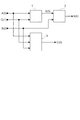
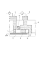
第1図は、第1の実施形態に係る1ビット加算器の構成を模式的に示すブロック図である。特にm=1、k=1とした場合に対応する。A(0),B(0)は、n桁(nは1以上の整数)の2進数値AおよびBの第i桁のビット値A[i]と、ビット値B[i]と、に対応する信号であり、C(−1)は、第i−1桁から第i桁への桁上げビット値C[i−1]に対応する下位桁からの桁上がり信号である。いずれも、ビット値0に対応する「0」またはビット値1に対応する「1」で表わされる入力のうちのいずれかに応じた電気信号で与えられる。ここで、iは、0からn−1の整数のうちのいずれかであり、iが0のとき、C(−1)は、「0」に対応した電気信号である。(First embodiment)
FIG. 1 is a block diagram schematically showing a configuration of a 1-bit adder according to the first embodiment. In particular, this corresponds to the case where m = 1 and k = 1. A (0) and B (0) are binary values A [i] of n digits (n is an integer of 1 or more) and the bit value A [i] of the i-th digit of B and the bit value B [i]. C (-1) is a carry signal from the lower digit corresponding to the carry bit value C [i-1] from the (i-1) th digit to the ith digit. Both are given by an electrical signal corresponding to one of the inputs represented by “0” corresponding to the
図1中に示す演算器1および2、3は、多入力論理演算器である。演算器1は、第1の波動演算器であり、A(0)とB(0)との入力に対し、中間出力X(0)を出力する。また、演算器2は、第2の波動演算器であり、演算器1の出力X(0)とC(−1)とを入力とし、S(0)を出力する。さらに、演算器3は、閾値波動演算器であり、A(0)とB(0)とC(−1)とを入力とし、C(0)を出力する。
The
表1は、演算器1の真理値表であり、表2は、演算器2の真理値の表である。すなわち、演算器1、2は、排他的論理和演算を行う。また、表3は、演算器3の真理値表を示しており、演算器3が閾値論理演算、すなわち3つの数の和が2以上なら1を出力し、1以下なら0を出力する演算を実行する。これらの真理値表には、2進数値AおよびBのビット値A[i]、B[i]および桁上げビット値C[i−1]、演算結果に対応するビット値S[i]、X[i]、C[i]が示されているが、各演算器に入力される信号A(0)およびB(0)、C(−1)と、演算結果S(0)およびX(0)、C(0)と、の関係に対応している。以下、表4ないし表7についても同様である。

表4は、本実施形態に係る演算器1および2、3の入力と出力の関係をまとめた真理値表である。表4から、A(0)およびB(0)、C(−1)を相互に入れ替えても出力は変わらない。例えば、B(0)とC(−1)を入れ替えても、出力S(0)およびC(0)は同じである。
図2は、第1の実施形態に係る1ビット加算器の変形例を模式的に示すブロック図である。図1に示す加算器の入力B(0)とC(−1)とを入れ替えた構成となっている。すなわち、A(0)とC(−1)とが、演算器1に入力され、演算器1の出力X(0)とB(0)が、演算器2に入力される構成となっている。
FIG. 2 is a block diagram schematically showing a modification of the 1-bit adder according to the first embodiment. The input B (0) and C (-1) of the adder shown in FIG. That is, A (0) and C (−1) are input to the
次に、本実施形態に係る演算器1ないし3の構成について説明する。
これらの演算器は、構成要素として、第1ないし3の波動伝達媒体である膜状の媒体(以下では連続膜と称す)と、連続膜の面上に設けられ、演算器の入力ビット値に応じた電気信号を与えることが可能な第1ないし第3の入力部と、同じ連続膜の面上に設けられ、波動の局所的な振幅の大きさに応じた大きさの電気信号を取り出すことのできる第1ないし第3の波動検出部と、を有している。Next, the configuration of the
These arithmetic units are provided as constituent elements on a film-like medium (hereinafter referred to as a continuous film) as the first to third wave transmission media, and on the surface of the continuous film, and the input bit value of the arithmetic unit is The first to third input units capable of providing corresponding electrical signals and the same continuous film are provided on the surface of the continuous film, and an electrical signal having a magnitude corresponding to the local amplitude of the wave is taken out. And first to third wave detectors capable of performing the above.
(波動演算器の実施例)
図3は、本実施形態に係る演算器1または2を示す模式図である。図3(a)は、正面図、また、図3(b)は、平面図を示している。(Example of wave computing unit)
FIG. 3 is a schematic diagram showing the
図3に示す演算器1または2は、波動演算器であり、連続膜11が図示しない基板の上に設けられ、連続膜11の上には、2つの入力部5と、スピン波を検出する波動検出部8と、が設けられている。また、連続膜11は、室温において強磁性を示す磁性層を、少なくとも1層含んでいる。
The
入力部5は、連続膜11との間に所定の接触面を有するように設けられ、連続膜11の表面に略垂直な方向に電圧を印加するか、または、連続膜11の表面に略垂直な方向に電流を流す。これにより、入力部5の直下の領域において、スピントルクが発生し、連続膜11を構成する磁性層にスピン波を励起することができる。
The
入力部5と連続膜11とが電気的に接続する接触面は、直径200nm面の円より小さいことが望ましい。接触面が直径200nmの円より大きい場合には、ボルテックス状あるいは多磁区の磁化構造が励起され、スピン波が複数の成分を含む複雑な構造となるため、制御が難しくなる。また、入力部5のサイズを小さくすることにより、演算器全体のサイズを小さくすることができる。
The contact surface where the
これらの理由により、入力部5の接触面は、長辺長さが200nm以下の楕円、もしくは、円形、多角形であることが望ましい。また、その範囲内であれば、励起されるスピン波による演算の制御が容易となる。
For these reasons, the contact surface of the
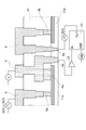
図4に示す各図は、入力部5と連続膜11の部分断面を示す模式図である。図4(a)に示す断面構造では、連続膜11は、表面から磁性層13/スペーサ層14/磁性層15の層構造となるように構成されている。また、非磁性導電材料からなる入力部5は、連続膜11の表面に設けられている。
Each figure shown in FIG. 4 is a schematic diagram showing a partial cross section of the
磁性層13は、スピン波の伝達媒体としての役割を担い、また、磁性層15は、入力部5から磁性層13を介して流れる電流により、磁性層13にスピントルクを付与し、スピン波を励起する。すなわち、磁性層13に与えられるスピントルクは、磁性層13の磁化方向M2と、磁性層15の磁化方向M1との間の角度に依存し、この角度が0°あるいは180°のとき、スピントルクの大きさはほぼ0となる。一方、スピントルクは、M1とM2との角度が0°から180°に変化する間で連続的に変化し、この間に極大となるM1とM2との角度が存在する。The
また、入力部5に印加する電圧の極性、または、入力部5と磁性層15の間を流れる電流の方向は、磁性層13および15の磁化方向との関係において、スピントルクが大きくなる電圧極性、または電流方向を選択することが望ましい。
The polarity of the voltage applied to the
通常、磁性層13の磁化方向M2に対して磁性層15の磁化方向M1が60°から120°となる範囲で、スピントルクが極大となる角度が含まれる。したがって、M1とM2との間の角度を、この範囲に設定することにより、少ない電流で大きなスピントルクを与える構成とすることができる。Usually, the magnetization direction M 1 of the
例えば、図4(a)に示す構造では、磁性層13の磁化方向M2は、連続膜11の表面に平行な方向とし、磁性層15の磁化方向M1は、連続膜の表面に垂直な方向としている。また、図4(b)では、磁性層13の磁化方向M2と磁性層15の磁化方向M1とを、共に連続膜11の表面に平行な方向とし、連続膜11の面内で略直交するように構成している。さらに、図4(c)では、磁性層13の磁化方向M2を連続膜11の表面に対して垂直とし、磁性層15の磁化方向を連続膜11の表面に平行としている。For example, in the structure shown in FIG. 4 (a), the magnetization direction M 2 of the
図4の各図に示した構造の内、図4(c)に示すように、磁性層13の磁化方向M2を連続膜11の表面に対して略垂直とすると、連続膜11の面内においてスピン波の伝播特性が等方的となり、伝播方向に依存しないというメリットを得ることができる。また、磁性層13は、スピン波伝達媒体であることから、スピントルクを効率的に受けることができ、また伝達損失が小さい材料を用いることが望ましい。Of the structures shown in each of FIGS. 4, as shown in FIG. 4 (c), when substantially perpendicular to the magnetization direction M 2 of the
連続膜11の表面に対して垂直に磁化する磁性材料として、例えば、FeVPd、また、FeCrPd、CoFePt等の合金を用いることができる。また、イットリウム鉄ガーネット(YIG)やマンガンフェライト等のフェライト系酸化物を用いると、スピン波の伝達損失を少なくすることができる。
As a magnetic material that is magnetized perpendicularly to the surface of the
これに対し、磁性層15は、一定のスピントルクを磁性層13に与えるために、磁化が固着されていることが望ましい。このため、磁性層15の層厚を10nm以上とすることが望ましい。あるいは、図4(b)および図4(c)に示すように、磁性層15に隣接して反強磁性層16を設けることにより、磁性層15の磁化方向M1を固着することができる。On the other hand, it is desirable that the
連続膜11の表面に略平行な磁化方向となる磁性層の材料としては、例えば、鉄(Fe)、コバルト(Co)、ニッケル(Ni)、マンガン(Mn)、クロム(Cr)よりなる群から選択された少なくとも一つの元素を含む磁性合金を用いることができる。また、反強磁性層16には、例えば、IrMn合金を使用することができる。
Examples of the material of the magnetic layer that has a magnetization direction substantially parallel to the surface of the
また、スペーサ層14は、磁性層13と磁性層15との間を移動する電子のスピン偏極が失われる長さ(スピン拡散長)よりも薄く設ける。さらに、連続膜11には、最上層として、磁性層13の上に保護膜を形成しても良い。保護膜は、スピン波を効率的に励起するために、導電性を有し、且つ、厚さが100nm以下であることが望ましい。
Further, the
スペーサ層14としては、トンネルバリア材料、または非磁性金属材料を用いることができる。トンネルバリア材料を用いると、読み出し時に大きな再生信号出力を得ることが可能となる。例えば、アルミニウム(Al)、チタン(Ti)、亜鉛(Zn)、ジルコニウム(Zr)、タンタル(Ta)、コバルト(Co)、ニッケル(Ni)、シリコン(Si)、マグネシウム(Mg)、鉄(Fe)よりなる群から選択された少なくとも一つの元素を含む酸化物、窒化物、フッ化物、酸窒化物を用いることができる。あるいは、GaAlAsなどの大きなエネルギーギャップを有する半導体を用いても良い。
As the
一方、スペーサ層14に非磁性金属材料を用いると、スピントルクを発生させるための電流注入を容易にすることができる。例えば、銅(Cu)、金(Au)、銀(Ag)、アルミニウム(Al)、また、これらよりなる群から選択された少なくとも一つの元素を含む合金を使用することができる。この場合、スペーサ層を1.5nm以上、20nm以下の厚さとすると、磁性層13と磁性層15とが層間結合せず、且つ、電子のスピン偏極を保持することができる。
On the other hand, when a nonmagnetic metal material is used for the
さらに、連続膜11の最上層に設ける保護膜としては、Ta、Ru、銅(Cu)、金(Au)、銀(Ag)、アルミニウム(Al)、また、これらよりなる群から選択された少なくとも一つの元素を含む合金、グラフェンなどの材料を用いることができる。
Furthermore, the protective film provided on the uppermost layer of the
また、入力部5に使用される非磁性導電材料は、例えば、銅(Cu)、金(Au)、銀(Ag)、アルミニウム(Al)、また、これらよりなる群から選択された少なくとも一つの元素を含む合金とすることができる。さらに、非磁性導電材料として、カーボンナノチューブやカーボンナノワイヤ、グラフェン等の材料を用いることもできる。
The nonmagnetic conductive material used for the
図5は、波動検出部8と連続膜11との部分断面を示す模式図である。波動検出部8は、連続膜11の上に接触面を介して設けられている。入力部5の直下で発生し連続膜11を伝播したスピン波は、波動検出部8において、合成信号として検出される。また、図5の各図における磁化方向の構成は、図4に示す、連続膜11の部分断面の各構造に対応する。すなわち、入力部5側と、波動検出部8側とにおいて、連続膜11に含まれる磁性層13および15の磁化方向は同じである。
FIG. 5 is a schematic diagram showing a partial cross section of the
図5(a)に示す構成では、磁性層15の磁化方向M1は、連続膜11の表面に垂直な方向であり、磁性層13の磁化方向M2は、連続膜11の表面に平行な方向となっている。また、図5(b)では、磁性層15の磁化方向M1および磁性層13の磁化方向M2が、共に連続膜11の表面に平行となっている。さらに、M1とM2とは、連続膜11の面内で直交している。また、図5(c)に示す構成では、磁性層15の磁化方向M1は、連続膜11の表面に平行であり、磁性層13の磁化方向M2は、連続膜11の表面に垂直な方向となっている。In the configuration shown in FIG. 5A, the magnetization direction M 1 of the
図5に示す連続膜11は、磁性層13および15でスペーサ層14を挟んだ構造となっており、波動検出部8から連続膜11に電圧を印加するか、または電流を流すことにより、TMR効果(Tunnel Magnetoresistance effect)もしくはGMR効果(Giant Magnetoresistance effect)により磁化の変化、すなわち、スピン波を検出することができる。通常、スピン波による信号変化は小さいので、2つの磁性層13および15の磁化方向は、略直交するように配置した、図5に示すいずれかの構造とし、検出感度を上げることが望ましい。特に、図5(b)に示した磁化配置は、磁性層13の磁化がともに面内方向であり、磁性層13の磁化方向の面内方向の変化を検出するのに適した構成となっているため、望ましい。
The
図6は、本実施形態に係る演算器1および2の部分断面を示す模式図である。
図示しない基板上に、絶縁膜を介して連続膜11aおよび11bが設けられている。連続膜11aの表面には、入力部5aと動検出部8aが接続されている。連続膜11a、および入力部5a、波動検出部8aは、例えば、演算器1を構成する。さらに、連続膜11bには、入力部5bと、図示しない波動検出部と、が接続され、演算器2を構成する。FIG. 6 is a schematic diagram showing a partial cross section of the
入力部5aには、入力電極6が接続されており、例えば、入力A(0)またはB(0)に対応する電気信号が印加される。その結果、入力部5aの直下でスピン波が励起され、連続膜11aに沿って波動検出部8aに向かって伝播する。一方、波動検出部8aには、出力電極9が接続されており、例えば、TMR効果を生じさせるためのバイアス電圧が印加されている。これにより、入力部5から伝播したスピン波は、TMR効果によって生じる電圧の変化として検出され、出力電極9の基板側の端子9aから電圧信号として出力される。
An
さらに、端子9aから出力された電圧信号は、増幅器22で増幅されてコンパレータ23に入力される。コンパレータ23では、入力された電圧信号と、閾値電圧Vthが比較され、例えば、電圧信号が閾値電圧Vthより大きい場合に、対応する電圧信号が出力される。
Further, the voltage signal output from the terminal 9 a is amplified by the
コンパレータ23の出力は、連続膜11b上に設けられた入力部5bに接続された入力電極6の端子6aに入力される。すなわち、コンパレータ23の出力は、例えば、演算器1から出力されるX(0)に該当し、演算器2の入力端子6aに入力される。
The output of the
増幅器22やコンパレータ23は、連続膜11aおよび11bと同一の面に配置すること、また、図6中に示す絶縁膜21の上下のいずれかに配置することも可能である。例えば、図6中に示すように、連続膜11の下層に配置することにより、演算器の集積度を高めることが可能である。具体的には、シリコン基板の表面に、増幅器22およびコンパレータ23を含む集積回路を形成した後、さらに連続膜11および入力部5、波動検出部8等を形成し、図6中に示すように、電気的な接続を取ることにより実施することができる。
The
図7は、図6に示す出力電極9の端子9aから出力される電圧信号の例を示す模式図である。図7(a)は、波動検出部8で検出されたスピン波の振幅が相対的に大きい場合の電圧波形であり、図7(b)は、スピン波の振幅が相対的に小さい場合の電圧波形を示している。一般に、TMR効果あるいはGMR効果において、2層以上の磁性層を含む積層膜の電気抵抗は、各磁性層の磁化方向の相対角度に依存して変化する。スピン波の振幅は磁化方向の時間的変化であるから、磁性層13を伝播するスピン波の振幅の大きさに応じて、磁性層13の磁化方向と、磁性層15の磁化方向と、の間の相対角度が変化し、連続膜11の抵抗を変化させる(図5参照)。したがって、入力部5aで励起されたスピン波の振幅が大きいほど、波動検出部8の直下における連続膜11の抵抗変化が大きくなり、端子9aに出力される電圧の変化が大きくなる。
FIG. 7 is a schematic diagram illustrating an example of a voltage signal output from the terminal 9a of the
例えば、図6中に示すコンパレータ23の入力端子(IN)に、図7に示す電圧信号を入力し、基準電圧の入力端子(REF)に、閾値電圧として図7中に示すVthを入力する。入力端子(IN)に入力される信号の大きさがVthを超えた場合、コンパレータ23の出力は、1に対応する電圧を出力し、入力端子(IN)に入力される信号の大きさがVth超えない場合、コンパレータ23の出力は、0に対応する電圧を出力するように、設定することができる。これにより、コンパレータ23は、図7(a)に示す、信号電圧がVthを超える時間においてのみ、1に対応する信号電圧を出力する。
For example, the voltage signal shown in FIG. 7 is input to the input terminal (IN) of the
なお、図6では、出力電極9の端子9aから出力される電圧信号を、増幅器22で増幅する構成としているが、波動検出部8で検出される抵抗変化が十分に大きい場合には、直接コンパレータ23の入力端子(IN)に電圧信号を入力することも可能である。また、コンパレータ23や増幅器22は、標準的な集積回路技術を用いて構成することができる。
In FIG. 6, the voltage signal output from the terminal 9a of the
次に、演算器1、2における、入力部5および波動検出部8の配置について説明する。連続膜11に含まれる磁性層13の磁化方向を、連続膜11の表面に垂直となるように形成すると、スピン波の伝播特性が等方的となる(図4(c)参照)。また、磁性層13としてスピン波の伝達損失の少ない材料を用いれば、入力部5および波動検出部8の配置に関する制約が小さくなり、さまざまな配置が可能となる。
Next, the arrangement of the
図8は、演算器1および2における、2つの入力部5と、波動検出部8と、の配置例を示す模式図である。図8(a)および(b)、(c)は、波動検出部8と入力部5との間隔dが等しくなるように配置した例である。図8(b)に示すように、波動検出部8と入力部5とが、直線上にあっても良いし、図8(a)、(c)に示すように、波動検出部8から等間隔な位置に、入力部5を任意に配置しても良い。このような配置とすることにより、2つの入力部5で発生したスピン波が、それぞれ連続膜11を伝播して波動検出部8に到達するまでの時間が等しくなる。これにより、2つの入力部5に入力される信号の同期をとる上で有利となる。
FIG. 8 is a schematic diagram illustrating an arrangement example of the two
また、図8(d)に示すように、入力部5の径rが、入力部5と波動検出部8との間隔dの2倍以上となるようにすれば、入力部5で励起されるスピン波の波長を、間隔dに比べて長くすることができる。これにより、入力部5と波動検出部8との間隔dが、2つの入力部5の間で異なっていても、波動検出部8に到達するスピン波の位相差を小さくすることができる。
Further, as shown in FIG. 8 (d), if the diameter r of the
前述したように、入力部5と連続膜11とが電気的に接続する接触面は、直径200nm面の円より小さいことが望ましい。したがって、例えば、入力部5が全面で連続膜に接触する場合、入力部の径rは、200nm以下とすることが望ましい。一方、波動検出部8の大きさは、入力部5の大きさに関係なく設定することができるが、検出するスピン波の位相を均一に保持して出力信号の減衰を防ぐために、連続膜11との接触面を小さくすることが望ましい。しかし、波動検出部8を小さくしすぎると、連続膜11との接触面の電流密度が高くなり、検出動作時に大きなスピントルクが働いて、意図しないスピン波を励起してしまう場合がある。したがって、意図しないスピン波を励起しない範囲で、波動検出部8の接触面を小さくすることが望ましい。少なくとも、波動検出部8のサイズは、検出するスピン波の波長より小さいことが望ましい。
As described above, the contact surface where the
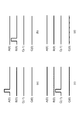
図9は、演算器1または2に入力される信号A(0)、B(0)と、出力信号X(0)と、の関係を示すタイミングチャートである。横軸に時間を取り、各信号の波形を模式的に示している。例えば、「1」が入力される場合には、入力のタイミングに合わせて、パルス形状の波形が表示されている。「0」の場合は、信号波形は平坦であり、パルス形状の波形は表示されない。(以下、タイミングチャートについては、同様に表示)
入力信号A(0)、B(0)の波形に対応して、信号値が「1」に該当する期間、入力部5に電圧V1を印加する。あるいは、入力部5から連続膜11へ電流I1を流す。一方、信号値が「0」のときは、電圧V0を印加する。あるいは、電流I0を流す。例えば、信号値が「0」の場合に、V0=0、あるいはI0=0とすれば、信号値「1」の場合との区別が容易となるので好ましい。FIG. 9 is a timing chart showing the relationship between the signals A (0) and B (0) input to the
Corresponding to the waveforms of the input signals A (0) and B (0), the voltage V 1 is applied to the
図9(a)では、入力信号A(0)、B(0)が、それぞれ「1」であるから、所定のタイミングで入力部5に電圧V1を一定時間印加する。例えば、図8(a)または(b)、(c)に示すように、入力部5と波動検出部8との間の間隔dが、2つの入力部5の間で等しい演算器の場合、信号A(0)が入力される入力部5と、信号B(0)が入力される入力部5と、に電圧V1を印加するタイミングは、励起されるスピン波の位相が半波長ずれるように設定することが望ましい。例えば、図9(a)中に示すように、信号B(0)が入力される入力部5に、電圧V1を印加するタイミングは、式(3)で算出される時間だけ遅らせるように設定する。In FIG. 9A, since the input signals A (0) and B (0) are “1”, the voltage V 1 is applied to the
tr=(2f)−1 ・・・(式3)
ここで、fはスピン波の周波数である。 tr = (2f) -1 (Formula 3)
Here, f is the frequency of the spin wave.
これにより、2つの入力部5で発生したスピン波が、波動検出部8に到達した時に、位相が半波長ずれることになる。その結果、2つのスピン波の合成波の振幅が減衰し、波動検出部8で検出される抵抗変化が小さくなる。したがって、例えば、図6に示す端子9aから出力される電圧信号が小さくなり、演算器からの出力信号X0は、「0」となる。
Accordingly, when the spin waves generated at the two
図9(b)では、信号A(0)は、「0」であり、信号B(0)は、「1」である。したがって、信号A(0)が入力される入力部5には、電圧が印加されず、信号B(0)が入力される入力部5に、電圧V1が印加される。この場合、信号A(0)が入力された入力部5ではスピン波が励起されず、信号B(0)が入力された入力部5のみでスピン波が励起される。したがって、スピン波の干渉は生じないので、波動検出部8は、信号B(0)の入力により励起されたスピン波を検出し、出力信号X(0)は、「1」となる。In FIG. 9B, the signal A (0) is “0”, and the signal B (0) is “1”. Therefore, the signal A (0) is the
図9(c)では、信号A(0)が、「1」であり、信号B(0)は、「0」である。この場合も、スピン波は、信号A(0)が入力される入力部5のみで励起され、出力信号X(0)は、「1」となる。また、図9(d)では、信号A(0)、B(0)が、共に「0」であり、スピン波は励起されず、出力信号X(0)も「0」となる。
In FIG. 9C, the signal A (0) is “1”, and the signal B (0) is “0”. Also in this case, the spin wave is excited only by the
図10は、演算器1または2に入力される信号A(0)、B(0)と、出力X(0)と、の関係を示す、別のタイミングチャートである。
FIG. 10 is another timing chart showing the relationship between the signals A (0) and B (0) input to the
スピン波による演算を行う場合、入力部5に、電圧V1を印加する時間、あるいは電流I1を流す時間は、ある程度、任意に設定することができる。例えば、図10に示すように、信号A(0)、B(0)のそれぞれの波形に対応して、電圧V1を印加(オン)してからオフするまでの時間を長くすることができる。In the case of performing the calculation using the spin wave, the time for applying the voltage V 1 or the time for flowing the current I 1 to the
図10(a)では、信号A(0)、B(0)は、ともに「1」であり、信号A(0)が入力される入力部5に電圧V1が印加されるタイミングと、信号B(0)が入力される入力部5に電圧V1が印加されるタイミングと、は、trだけずらしている。さらに、電圧V1が印加されている時間tA、tBを等しくしておけば、スピン波が干渉して減衰し、出力信号X(0)は、「0」となる。In FIG. 10 (a), the signal A (0), B (0) are both "1", the timing at which the voltage V 1 is applied to the
図10(b)では、信号A(0)は、「0」であり、信号B(0)は、「1」である。信号B(0)が入力される入力部5に電圧V1が印加される時間は、tBである。この際、図10(b)中に示すように、波動検出部8側で出力信号X(0)が検出され始めた後で、電圧V1がオフされても良い。In FIG. 10B, the signal A (0) is “0”, and the signal B (0) is “1”. Signal B (0) time voltage V 1 is applied to the
図10(c)では、信号A(0)が、「1」であり、信号B(0)は、「0」である。この場合も、信号A(0)が入力される入力部5に電圧V1が印加される時間は、tAであり、波動検出部8側で出力信号X(0)が検出され始めた後で、電圧V1がオフされても良い。また、図10(d)では、信号A(0)、B(0)が、共に「0」であり、スピン波は励起されず、出力信号X(0)も「0」となる。In FIG. 10C, the signal A (0) is “1”, and the signal B (0) is “0”. Again, the signal A (0) time voltage V 1 is applied to the
図9に示すように、短い時間幅のパルス電圧でV1を印加すると、消費電力を抑えることができる。また、図10に示すように、長い時間幅の電圧V1を印加すると、波動の持続時間が長くなるため、検出の安定性を向上させることができる。また、信号A(0)、B(0)に対応して、入力部5に電流I1を流す場合も同様である。As shown in FIG. 9, by applying a V 1 with a pulse voltage of a short duration, power consumption can be suppressed. Further, as shown in FIG. 10, when a voltage V 1 having a long time width is applied, the duration of the wave becomes long, so that the detection stability can be improved. The same applies to the case where the current I 1 is supplied to the
図11は、演算器1および2における、2つの入力部5と、波動検出部8と、の別の配置例を模式的に示す平面図である。
図11に示す演算器では、2つの入力部5と、波動検出部8と、の間隔の内、一方の間隔を他方に比べてスピン波の波長λの半奇数倍だけ広くしている。図11中に示すnは、整数である。FIG. 11 is a plan view schematically showing another arrangement example of the two
In the computing unit shown in FIG. 11, one of the intervals between the two
図12は、図11に示す演算器に入力される信号A(0)、B(0)と、出力X(0)と、の関係を示すタイミングチャートである。 FIG. 12 is a timing chart showing the relationship between signals A (0) and B (0) input to the computing unit shown in FIG. 11 and output X (0).
図12(a)では、入力信号A(0)、B(0)が、それぞれ「1」であるから、信号A(0)が入力される入力部5と、信号B(0)が入力される入力部5と、に、同時に電圧V1を印加する。2つの入力部5と波動検出部8との間隔の内、一方の間隔が他方に比べてスピン波の波長λの半奇数倍だけ長いので、それぞれの入力部5で励起された2つのスピン波は、波動検出部8に到達する時点で位相が半波長分ずれている。これにより、2つのスピン波の合成波の振幅が減衰し、出力される電圧信号が小さくなる。したがって、図12(a)中に示すように、出力信号X(0)は、「0」となる。In FIG. 12A, since the input signals A (0) and B (0) are “1”, the
図12(b)、(c)では、信号A(0)、B(0)の一方は、「0」であり、他方は、「1」である。したがって、2つの入力部5の片方のみでスピン波が励起され、干渉は生じない。波動検出部8は、いずれかの入力部5で励起されたスピン波を検出し、出力信号X(0)は、「1」となる。また、図9(d)では、信号A(0)、B(0)が、共に「0」であり、スピン波は励起されず、出力信号X(0)も「0」となる。
In FIGS. 12B and 12C, one of the signals A (0) and B (0) is “0” and the other is “1”. Accordingly, the spin wave is excited by only one of the two
(閾値波動演算器の実施例)
図13は、演算器3における、3つの入力部5と、波動検出部8と、の配置例を模式的に示す平面図である。演算器3は閾値波動演算器であり、入力部5および波動検出部8、連続膜11の断面構造は、波動演算器である演算器1または2と同じにすることができる。(Example of threshold wave calculator)
FIG. 13 is a plan view schematically showing an arrangement example of the three
図13(a)に示す例では、3つの入力部5と、波動検出部8と、の間隔dが、それぞれ等しい。したがって、3つの入力部5に同時に入力された電圧、もしくは電流により、それぞれ励起された3つのスピン波は、波動検出部8に位相差なく同時に到達する。その結果、波動検出部8では、それぞれスピン波の振幅の和に等しい振幅を有する合成波が検出される。
In the example shown in FIG. 13A, the distances d between the three
これにより、例えば、波動検出部8に接続された端子9a(図6参照)からは、波動検出部8に到達したスピン波の数に対応する大きさの電圧信号が出力される。この電圧信号と、所定の閾値電圧と、を比較することにより、例えば、スピン波、すなわち信号「1」の数が、所定数より多い場合に、「1」を出力し、所定数を下回る場合に、「0」を出力する閾値演算器として機能させることができる。具体的には、図6のコンパレータ23のREF端子に閾値電圧を入力し、信号電圧との比較結果を出力させる。
Thereby, for example, a voltage signal having a magnitude corresponding to the number of spin waves reaching the
図13(b)に示す例では、励起されるスピン波の波長が、入力部5と波動検出部8との間隔dより長くなるように、3つの入力部5の直径rを、相対的に大きく形成する。これにより、3つの入力部5で同時に励起されたスピン波が、波動検出部8に到達する時の位相差を小さくすることができる。その結果、波動検出部8で検出される合成波の振幅の大きさが、3つの入力部5で励起されたスピン波の数に対応し、閾値演算器として機能することができる。
In the example shown in FIG. 13B, the diameters r of the three
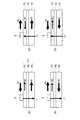
図14および図15は、演算器3に入力される信号A(0)、B(0)、C(−1)と、出力C(0)と、の関係を示すタイミングチャートである。演算器3は閾値演算器であり、信号「1」が2つ以上入力されると、出力C(0)に「1」を出力し、信号「1」が1つ以下であると、出力C(0)に「0」を出力する。
14 and 15 are timing charts showing the relationship between the signals A (0), B (0), C (-1) input to the
図14(a)では、入力信号A(0)、B(0)、C(−1)が、それぞれ「1」であるから、信号A(0)が入力される入力部5と、信号B(0)が入力される入力部5と、信号C(−1)が入力される入力部5と、に、同時に電圧V1を印加される。例えば、図13(a)の配置例に従う演算器であれば、それぞれの入力部5で励起された3つのスピン波は、波動検出部8に到達して合成され、入力部5で励起されたスピン波の3倍の振幅を有する合成波が、波動検出部8で検出される。これにより、出力C(0)に「1」が出力される。In FIG. 14A, since the input signals A (0), B (0), and C (−1) are “1”, the
図14(b)、(c)、(d)では、信号A(0)、B(0)、C(−1)の内、2つの入力は、「1」であり、残る1つは、「0」である。したがって、3つの入力部5の内、2つでスピン波が励起される。波動検出部8では、2つのスピン波が合成された合成波が検出され、出力C(0)に、「1」が出力される。
In FIGS. 14B, 14C, and 14D, two inputs of the signals A (0), B (0), and C (−1) are “1”, and the remaining one is “0”. Accordingly, spin waves are excited by two of the three
また、図15(a)、(b)、(c)では、信号A(0)、B(0)、C(−1)の内、1つの入力は、「1」であり、残る2つは、「0」である。したがって、3つの入力部5の内、いずれか1つでスピン波が励起され、波動検出部8では、励起されたスピン波を検出する。しかしながら、出力される電圧信号は、閾値電圧より低いので、出力C(0)には、「0」が出力される。図9(d)では、信号A(0)、B(0)、C(−1)は、全て「0」であり、スピン波は励起されず、出力C(0)も「0」を出力する。
Further, in FIGS. 15A, 15B, and 15C, one of the signals A (0), B (0), and C (-1) is “1”, and the remaining two Is “0”. Therefore, a spin wave is excited by any one of the three
(変形例1)
図16は、第1の実施形態の変形例に係る演算器の入力部5および連続膜を模式的に示す部分断面図である。本変形例に係る演算器では、連続膜11の周辺に、永久磁石あるいは配線磁界等の外部磁界の付与部を設け、磁性層13の磁化に作用させる構成とする。(Modification 1)
FIG. 16 is a partial cross-sectional view schematically showing the
外部磁界が磁性層13の磁化に作用を及ぼす構成とした場合、入力部5に印加される電圧または電流の信号により生じるスピントルクによる磁化方向M2と、外部磁界による磁化方向H0と、が競合するように構成すれば、スピン波の安定した発振状態が得られ、スピン波を効率よく発生させることができる。例えば、図16(a)および(b)に示す構成では、連続膜11の表面に平行に磁化した磁性層15の磁化方向M1と、外部磁界の方向H0と、が逆向きで、双方の間の角度が180度に近い状態となっている。この場合、入力部5から、磁性層13を介して磁性層15に向けて電流J1を流すと、磁性層13を磁性層15と同じ方向M1に磁化させようとするスピントルクが作用する。一方、外部磁界からは、磁性層15と逆向きの方向H0に磁化させようとする作用が働いている。この結果、両方の作用が競合し、スピン波を容易に励起することができる。When the external magnetic field acts on the magnetization of the
一方、図16(c)および(d)に示す構成では、外部磁界の方向H0と、磁性層15の磁化方向M1は一致している。この場合、磁性層15から磁性層13を介して入力部5に向けて電流J2を流すと、磁性層15の磁化方向M1に対して逆向きの方向M2に磁性層13を磁化させようとするスピントルクが作用する。この結果、外部磁界の作用と、スピントルクの作用と、が競合するようになり、スピン波の励起を容易にすることができる。On the other hand, in the configuration shown in FIGS. 16C and 16D, the direction H 0 of the external magnetic field and the magnetization direction M 1 of the
図17は、外部磁界付与部18を設けた本変形例に係る演算器の断面を示す模式図である。
FIG. 17 is a schematic diagram showing a cross section of a computing unit according to this modification in which the external magnetic
図示しない基板上に、絶縁膜21を介して連続膜11が設けられ、連続膜11の表面には、入力部5および波動検出部8が接続されている。また、入力部5は、入力電極6に接続し、波動検出部8は、出力電極9に接続されている。さらに、連続膜11の上方に絶縁膜21を介して外部磁界付与部18が設けられている。外部磁界付与部18には、永久磁石を使用しても良いし、また、図の奥行き方向に伸びる金属配線として形成し、その金属配線に電流を流して発生する磁界を連続膜11に作用させる構成としても良い。
A
(変形例2)
図18は、第1の実施形態の第2の変形例に係る演算器の入力部5および連続膜11を模式的に示す部分断面図である。本変形例では、連続膜11に含まれる磁性層は1層である。(Modification 2)
FIG. 18 is a partial cross-sectional view schematically showing the
図18(a)では、図示しない基板上に形成された磁性層25に、非磁性の導電性材料を用いて形成された入力部5が接続されている。連続膜11は、磁性層25そのものであり、また、磁性層25の磁化方向M3は、磁性層25の表面に垂直となるように形成されている。In FIG. 18A, an
このように、磁性層が一層であっても、入力部5を形成することにより局所的に磁気異方性が異なる部分が生じ、入力部5へ電圧を印加するか、もしくは、入力部5を介して磁性層25に電流を流すことにより、スピントルクが発生しスピン波が励起される。また、磁化方向M3が磁性層25の表面に垂直であることから、磁性層25内を伝播するスピン波の伝播特性が等方的となる。As described above, even if the magnetic layer is a single layer, the formation of the
また、図18(b)に示すように、磁性層25の磁化方向M3を磁性層25の表面に平行に形成することもできる。この場合、入力部5が設けられた面の反対側に反強磁性層16を設け、磁性層25中の磁化方向M3を固着することが望ましい。このようにすることで、入力信号以外の要因で連続膜25中にスピン波が発生することを防ぐことができる。このように、磁化方向が表面に平行な磁性層は、容易に製造できるという利点がある。Further, as shown in FIG. 18 (b), may be formed parallel to the magnetization direction M 3 of the
さらに、磁性層25の表面には、キャップ層として図示しない導電性保護膜を形成しても良いし、図18(c)に示すように、磁性層25と入力部5との間に絶縁層26を設けてもよい。
Further, a conductive protective film (not shown) may be formed on the surface of the
図19は、第2の変形例に係る演算器の断面(a)および平面(b)を示す模式図である。本変形例に係る演算器は、図19(a)に示すように、連続膜11に接続して設けられた入力部5と、入力電極6と、さらに、絶縁膜21を介して設けられた波動検出部28を有している。
FIG. 19 is a schematic diagram showing a cross section (a) and a plane (b) of a computing unit according to the second modification. As shown in FIG. 19A, the computing unit according to this modification is provided via the
波動検出部28は、図19(b)に示すように、平行に形成されたコプレーナ線路28aおよび28bであり、連続膜11中を伝播するスピン波による磁界の変化を電磁誘導作用により検出する。すなわち、入力電極6から入力された信号により入力部5で励起されたスピン波が、連続膜11中を伝播し、そのスピン波による磁界の変化を、波動検出部28で高周波の誘導電流として検出し、さらに出力することができる。また、コプレーナ線路の代わりにマイクロストリップライン等の各種導波路を用いることができる。
As shown in FIG. 19B, the wave detection unit 28 includes
(変形例3)
図20は、第3の変形例に係る入力部7の部分断面(a)、および、波動検出部8の部分断面(b)を示す模式図である。(Modification 3)
FIG. 20 is a schematic diagram illustrating a partial cross section (a) of the
本変形例では、図20(a)に示すように、入力部7も導電性の磁性体で形成される。さらに、入力部7と磁性層25との間にはスペーサ層14が設けられる。このような構造でも、入力部7に電圧を印加するか、または、入力部7からスペーサ層14を介して磁性層25に電流を流すことにより、スピン波を励起することができる。この際、スピン波の励起をより低エネルギーで行うために、入力部7の磁化方向M5と磁性層25の磁化方向M4とは、直交することが望ましい。In this modification, as shown in FIG. 20A, the
一方、磁性層25中を伝播するスピン波を検出する波動検出部は、図19(b)に示すコプレーナ線路28aおよび28bとすることができる。また、図20(b)に示すように、磁性層25と、スペーサ層14と、磁性層27と、が積層された層構造の表面に波動検出部8が設けられた構成とすることができる。図20(b)に示す構成とすることにより、TMR効果やGMR効果を用いてスピン波を検出することができる。
On the other hand, the wave detector for detecting the spin wave propagating in the
(変形例4)
図21は、第4の変形例に係る演算器1および2の部分断面を示す模式図である。(Modification 4)
FIG. 21 is a schematic diagram showing a partial cross section of the
本変形例では、演算器1の端子9aから出力される電圧信号が、ローパスフィルタ32を介して、演算器2の入力端子6aに入力される構成となっている。また、端子9aとローパスフィルタ32との間には、整流用のダイオード31が配置されている。これにより、演算器1から出力される電圧信号を、単一極性の信号に変換して演算器2に入力することができる。なお、演算器1から出力される電気信号の波形に応じて、ローパスフィルタ32のない実施形態とすることが可能である。
In this modification, the voltage signal output from the terminal 9a of the
(変形例5)
図22は、第5の変形例に係る演算器を模式的に示す斜視図である。本変形例に係る演算器においても、連続膜11の上に、非磁性導電材料からなる2つの入力部5と波動検出部8とが設けられている。連続膜11は、表面から磁性層13/スペーサ層14/磁性層15の層構造となるように構成されている。また、本変形例における波動検出部8は、図22中に示すように、非磁性導電材料からなる配線として設けられている。(Modification 5)
FIG. 22 is a perspective view schematically showing a computing unit according to the fifth modification. Also in the arithmetic unit according to this modification, two
すなわち、磁性層13においてスピン波が励起されると、その振幅の大きさに応じたスピン流が、波動検出部8として設けられた配線に流入する。そうすると、非磁性体である配線において、スピン−軌道相互作用の効果のために、スピン流の大きさに応じた電流が配線中を流れる。このような現象は、逆スピンホール効果と呼ばれる。結果として、スピン波の振幅の大きさを、配線を流れる電流の大きさに変換して検出することができる。
That is, when a spin wave is excited in the
この際、検出感度を大きくするために、配線に用いる非磁性導電材料として、スピン−軌道相互作用が大きい物質を含む材料を用いることが望ましい。具体的には、原子番号が37以上の物質は、スピン−軌道相互作用が大きいので好適である。例えば、白金Ptや金Au、あるいは、これらを含む合金を用いることができる。 At this time, in order to increase detection sensitivity, it is desirable to use a material containing a substance having a large spin-orbit interaction as the nonmagnetic conductive material used for the wiring. Specifically, a substance having an atomic number of 37 or more is preferable because the spin-orbit interaction is large. For example, platinum Pt, gold Au, or an alloy containing these can be used.
また、図22に示した演算器は、演算器1または2の構成を有する波動演算器であるが、演算器3の構成を有する閾値波動演算器においても、本実施例に係る波動検出器8を用いることができる。
The computing unit shown in FIG. 22 is a wave computing unit having the configuration of
(変形例6)
図23は、第6の変形例に係る演算器3を示す模式図である。図23(a)は、正面図を示し、図23(b)は、平面図を示している。本変形例では、図示しない基板上に連続膜34が設けられ、連続膜34上に3つの入力部35と波動検出部38とが設けられている。連続膜34は、圧電体からなる表面層を有している。(Modification 6)
FIG. 23 is a schematic diagram showing a
入力部35は、第1電極35aと第2電極35bとからなる電極対を有する。この第1電極35aと第2電極35bとの間に、入力信号に対応したパルス電圧あるいは交流電圧を印加することにより圧電体の表面が歪み、表面弾性波が発生する。表面弾性波は、第1電極35aと第2電極35bとの間隔に対応した波長を有し、連続膜34の表面に沿って伝播する。
The
この際、表面弾性波の伝播特性は、圧電体の結晶性に依存し、結晶方位に応じた方向に伝播する。特に、単結晶の圧電体では、均一な表面弾性波が励起されるので、連続膜34の表面層、もしくは、連続膜34を、単結晶の圧電体で形成することが望ましい。
At this time, the propagation characteristic of the surface acoustic wave depends on the crystallinity of the piezoelectric body and propagates in a direction corresponding to the crystal orientation. In particular, since a uniform surface acoustic wave is excited in a single crystal piezoelectric body, it is desirable to form the surface layer of the
さらに、各入力部35で励起される表面弾性波の波長を同じにするために、例えば、各入力部35の間で、電極形状を同一とし、第1電極35aと第2電極35bとの間隔を等しくすることが望ましい。
Furthermore, in order to make the wavelength of the surface acoustic wave excited by each
一方、連続膜34上に設けられた波動検出部38は、図23(b)に示すように、櫛形に形成された2つの電極38aおよび38bが入れ子状に配置された構成となっている。各入力部35で励起され、連続膜34の表面を伝播した表面弾性波は、波動検出部38の位置で合成される。そして、波動検出部38では、合成波の振幅に応じた電気信号を、圧電効果により取り出すことができる。
On the other hand, the
この際、線形に形成された電極38aおよび38bの長辺は、入力部35の方向に垂直となるように配置されることが望ましい。すなわち、入力部35から波動検出部38に向かう表面弾性波の伝播方向に直交するように配置することで、表面弾性波の検出効率を向上させることができる。また、入力部35から波動検出部へ向かう方向(図23中の横方向)を、表面弾性波の伝播速度が最大となる結晶方向に合わせることが望ましい。
At this time, the long sides of the linearly formed
さらに、第1電極35aと第2電極35bとの間隔と、波動検出部38の櫛形電極38aと38bとの間隔と、を一致させることにより、入力部35で励起された弾性波のみを検出することができる。
Furthermore, by matching the distance between the
図23に示した演算器では、各入力部35から波動検出部38までの距離を一定としており、入力部35に電圧を印加するタイミングを合わせることにより、波動検出部38の位置で合成される各表面弾性波の位相を合わせることができる。これにより、閾値波動演算器として機能させることが可能となる。
In the arithmetic unit shown in FIG. 23, the distance from each
一方、連続膜34上に設けられる入力部35を2つとして、各入力部35から波動検出部38(合成位置)までの距離を、表面弾性波の半波長分ずらすことにより、合成される表面弾性波を逆位相とすることができる。これにより、排他的論理和演算を実行する波動演算器として機能させることも可能である。
On the other hand, two
また、波動検出部38の位置で合成される表面弾性波の位相を逆転させる方法として、入力部35に電圧を印加するタイミングを、半波長の伝播時間分だけずらす方法、または、いずれかの入力部35において、第1電極35aおよび第2電極35bに印加する電圧の極性を逆にする方法を用いることもできる。
Further, as a method of reversing the phase of the surface acoustic wave synthesized at the position of the
(第2の実施形態)
図24は、第2の実施形態に係る加算器を示すブロック図である。本実施形態に係る加算器は、m+1ビット加算器40であり、2進数値Aの第i桁ないし第(i+m)桁のビット値に対応する信号であるA(0)ないしA(m)と、2進数値Bの第i桁ないし第(i+m)桁のビット値に対応する信号であるB(0)ないしB(m)と、2進数値Aと2進数値Bとの和の第(i−1)桁から第i桁への桁上げビット値に対応する信号であるC(−1)と、に対応する信号の入力に対し、演算結果S(0)ないしS(m)、およびC(m)を出力する加算器である。ここでmは、0以上の整数である。(Second Embodiment)
FIG. 24 is a block diagram showing an adder according to the second embodiment. The adder according to this embodiment is an m + 1
A(0)ないしA(m)、およびB(0)ないしB(m)、C(−1)は、「0」または「1」で表わされる2つの入力のうちのいずれかであり、加算器の入力端子には、「0」または「1」のそれぞれに応じた電気信号が入力される。一方、出力端子には、同じく「0」または「1」のいずれかであるS(0)ないしS(m)、およびC(m)に対応する信号が出力される。 A (0) to A (m) and B (0) to B (m), C (−1) are either one of two inputs represented by “0” or “1”, and are added An electrical signal corresponding to each of “0” or “1” is input to the input terminal of the device. On the other hand, signals corresponding to S (0) to S (m) and C (m), which are either “0” or “1”, are output to the output terminal.
また、図24中に示すように、m+1ビット加算器40は、mビット加算器41、演算器3m+1、演算器3m+2、演算器3m+3を有する加算器と考えることができる。
Further, as shown in FIG. 24, the m + 1
さらに、mビット加算器41は、m−1ビット加算器と、演算器3m−2、演算器3m−1、演算器3mを有し、A(0)ないしA(m−1)と、B(0)ないしB(m−1)と、C(−1)と、の入力に対し、S(0)ないしS(m−1)と、C(m−1)を出力する。
Further, the m-
またさらに、m−1ビット加算器は、m−2ビット加算器と、演算器3m−5と、演算器3m−4、演算器3m−3を有する加算器と考えられ、A(0)ないしA(m−2)と、B(0)ないしB(m−2)と、C(−1)と、の入力に対し、S(0)ないしS(m−2)と、C(m−2)と、を出力する。
Further, the m-1 bit adder is considered as an adder having an m-2 bit adder, an
一方、m=0の場合、加算器40は、図1に示す1ビット加算器であり、演算器1および演算器2、演算器3を有し、A(0)、B(0)、C(−1)を入力として、S(0)およびC(0)を出力する。
On the other hand, when m = 0, the
結局、m+1ビット加算器40は、演算器1ないし3m+3を有している。その内、演算器3k+1は、第1の波動演算器であり、A(k)とB(k)とを入力とし、中間出力X(k)を出力する。ここで、kは、0からmの整数である。演算器3k+1の真理値を、表5に示す。また、演算器3k+2は、第2の波動演算器であり、X(k)とC(k−1)とを入力とし、演算結果S(k)を出力する。演算器3k+2の真理値を、表6に示す。
表7に示す真理値表は、表5と表6とを結合し、入力A(k)とB(k)とC(k−1)とに対する演算結果S(k)を示している。表7から明らかなように、入力A(k)およびB(k)、C(k−1)のいずれかを入れ替えても、演算結果S(k)は変化しない。例えば、第1の波動演算器にA(k)、C(k−1)を入力し、第2の波動演算器にX(k)とB(k)を入力するように構成しても、演算結果S(k)は、上記の場合と変わらないことを示している。
さらに、演算器3k+3は、閾値波動演算器であり、A(0)ないしA(k)と、B(0)ないしB(k)と、C(−1)と、を入力とし、C(k)を出力する。また、演算器3k+3は、数式1にしたがって、2k+1に対応する閾値を基準として「0」または「1」に対応する信号を出力する。Further, the computing unit 3k + 3 is a threshold wave computing unit, and inputs A (0) to A (k), B (0) to B (k), and C (−1), and C (k ) Is output. Further, the arithmetic unit 3k + 3 outputs a signal corresponding to “0” or “1” based on the threshold value corresponding to 2 k + 1 according to
このとき、各入力信号に対して、重み付けを行う。すなわち、入力信号A(0)の重みを1とするとき、入力信号A(i)(iは0からkまでの整数)の重みが2i倍となるように重み付けを行う。具体的には、例えば、信号a(i)を与える入力電極を2i個設けることによって行うことができる。At this time, each input signal is weighted. That is, when the weight of the input signal A (0) is 1, weighting is performed so that the weight of the input signal A (i) (i is an integer from 0 to k) is 2 i times. Specifically, for example, it can be performed by providing 2 i input electrodes for providing the signal a (i).
あるいは、入力信号A(i)の大きさが入力信号A(0)の大きさの2i倍になるように電圧または電流を入力部に与えることによっても実施することができる。これにより、励起される波動の振幅の大きさに対して重み付けが行われ、その結果、数式1に示す閾値論理演算が実行される。
第1の波動演算器、および、第2の波動演算器、閾値波動演算器は、それぞれ、第1の実施形態において説明した波動演算器および閾値波動演算器と同様な構成とすることができる。 The first wave computing unit, the second wave computing unit, and the threshold wave computing unit can be configured similarly to the wave computing unit and the threshold wave computing unit described in the first embodiment, respectively.
図25は、m=1とした場合の2ビット加算器42を示すブロック図である。2ビット加算器42は、演算器51ないし56を有しており、A(0)、B(0)、A(1)、B(1)、C(−1)の入力に対し、S(0)、S(1)、C(1)を出力する。演算器51および演算器54は、第1の波動演算器であり、それぞれ中間出力X(0)およびX(1)を出力する。演算器52および演算器55は、第2の波動演算器であり、X(0)、C(−1)およびX(1)、C(0)の入力に対し、S(0)およびS(1)を出力する。さらに、閾値波動演算器である演算器53は、A(0)、B(0)、C(−1)の入力に対し、C(0)を出力し、演算器56は、A(0)、B(0)、A(1)、B(1)、C(−1)の入力に対し、C(1)を出力する。
FIG. 25 is a block diagram showing the 2-
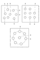
図26は、図25に示す2ビット加算器における演算器56の構成を模式的に示す平面図である。演算器56は、数式2に従って閾値論理演算を行う。すなわち、A(0)およびB(0)、C(−1)、さらに、それぞれ2つのA(1)およびB(1)を入力とし、C(1)を出力する。つまり、演算器56は、7入力1出力の演算器であり、図26(a)、(b)、(c)の各図に示すように、7つの入力部5と1つの波動検出部8とが設けられている。各入力部5で励起されたスピン波は、波動検出部8の位置で合成され、合成波に対応した信号が出力される。この際、波動検出部8で検出した信号強度が、閾値4に対応するレベルより高ければ、数式2にしたがって、「1」に対応する演算結果が出力され、閾値4を下回る信号レベルであれば、「0」に対応する演算結果が出力される。
また、前述したように、スピン波の波長に比べて、入力部5と波動検出部8との間隔が狭く、且つ、スピン波の伝播特性が等方的であり、また、伝播損失が小さければ、入力部7と波動検出部8は、図26(a)および(b)に示すように、任意に配置することができる。また、図26(c)に示すように、波動検出部8を中心として、入力部5を等距離に配置しても良い。
Further, as described above, if the distance between the
(第3の実施形態)
図27は、第3の実施形態に係るmビット加算器44を示すブロック図である。本実施形態に係る加算器44は、q個(qは1以上の整数)の部分加算器を備えている。例えば、図27中に示す例では、q=2であり、部分加算器45と、部分加算器46と、を備える。(Third embodiment)
FIG. 27 is a block diagram showing an m-
本実施形態に係る部分加算器は、2進数値AおよびBの第j桁ないし第(j+n−1)桁のビット値A[j]ないしA[j+n−1]、およびB[j]ないしB[j+n−1]と、桁上げビット値C[j−1]と、に対応する信号の入力に対し、演算結果S(j)ないしS(j+n−1)を出力する第1ないし第nの加算演算器と、桁上げビット値C[j+n−1]に対応する演算結果C(j+n−1)を出力する桁上げ演算器と、を有している。ここで、j、nは整数、また、i≦j、j+n≦i+mである。 In the partial adder according to the present embodiment, the bit values A [j] to A [j + n-1] and B [j] to B of the jth to (j + n-1) th digits of the binary values A and B are used. First to nth outputs of operation results S (j) to S (j + n-1) in response to inputs of signals corresponding to [j + n-1] and carry bit value C [j-1]. An adder arithmetic unit, and a carry arithmetic unit that outputs an arithmetic result C (j + n-1) corresponding to the carry bit value C [j + n-1]. Here, j and n are integers, and i ≦ j and j + n ≦ i + m.
第1の加算演算器は、A[j]およびB[j]、C[j−1]の内、2つに対応する信号を、第1の波動演算器に入力してX(j)を出力させる。さらに、A[j]およびB[j]、C[j−1]の内、第1の波動演算器に入力されなかった残りの一つに対応する信号と、X(j)と、を第2の波動演算器に入力して前記S(j)を出力させる。 The first addition computing unit inputs signals corresponding to two of A [j], B [j], and C [j−1] to the first wave computing unit and inputs X (j). Output. Further, a signal corresponding to the remaining one of A [j], B [j], and C [j−1] that has not been input to the first wave calculator and X (j) 2 to output the S (j).
また、第p(pは1からnまでの整数)の加算器は、A(j)ないしA(j+p−2)と、B(j)ないしB(j+p−2)と、C(j−1)と、を閾値波動演算器に入力してC(j+p−2)を出力させる。さらに、A(j+p−1)と、B(j+p−1)と、を、第1の波動演算器に入力してX(j+p−1)を出力させ、C(j+p−2)と、X(j+p−1)と、を第2の波動演算器に入力してS(j+p−1)を出力させる。 The p-th adder (p is an integer from 1 to n) includes A (j) to A (j + p−2), B (j) to B (j + p−2), and C (j−1). ) To the threshold wave calculator, and C (j + p−2) is output. Further, A (j + p−1) and B (j + p−1) are input to the first wave calculator to output X (j + p−1), and C (j + p−2) and X ( j + p−1) is input to the second wave calculator, and S (j + p−1) is output.
さらに、桁上げ演算器は、A(j)ないしA(j+n−1)、およびB(j)ないしB(j+n−1)と、C(j−1)と、を閾値波動演算器に入力してC(i+n−1)を出力させる。 Further, the carry calculator inputs A (j) to A (j + n-1), B (j) to B (j + n-1), and C (j-1) to the threshold wave calculator. To output C (i + n-1).
図27中に示す部分加算器45は、A(j)ないしA(j+n−1)、および、B(j)ないしB(j+n−1)、C(j−1)を入力として、S(j)ないしS(j+n−1)、およびC(j+n−1)を出力するnビットの部分加算器である。また、部分加算器46は、A(j+n)ないしA(j+n+w−1)、および、B(j+n)ないしB(j+n+w−1)、C(j+n−1)を入力として、S(j+n)ないしS(j+n+w−1)、およびC(j+n+w−1)を出力するwビットの部分加算器である。ここで、wは1以上の整数であり、n+w=mである。
The
例えば、n=4、w=4とすれば、部分加算器45および46は、4ビットの部分加算器であり、加算器44は、A(0)ないしA(7)、および、B(0)ないしB(7)、C(−1)を入力として、S(0)ないしS(7)、およびC(7)を出力する8ビット加算器と考えることができる。
For example, if n = 4 and w = 4, the
図28は、4ビット部分加算器45aの構成を示すブロック図である。4ビット部分演算器45aは、演算器51ないし62を有し、A(0)ないしA(3)、および、B(0)ないしB(3)、C(−1)を入力として、S(0)ないしS(3)、およびC(3)を出力する。演算器51および演算器54、演算器57、演算器60は、第1の波動演算器であり、演算器52および演算器55、演算器58、演算器61は、第2の波動演算器である。また、演算器53および演算器56、演算器59、演算器62は、閾値波動演算器である。
FIG. 28 is a block diagram showing a configuration of the 4-bit partial adder 45a. The 4-bit partial arithmetic unit 45a includes
第1の加算演算器は、A(0)およびB(0)を入力としてX(0)を出力する演算器51、および、C(−1)とX(0)を入力としてS(0)を出力とする演算器52で構成される。また、図2に示すように、B(0)とC(−1)との入力を入れ替えても、出力S(0)は変化しない。
The first addition arithmetic unit includes an
第2の加算演算器は、A(0)、B(0)、C(−1)を入力としてC(0)を出力する演算器53と、A(1)、B(1)を入力としてX(1)を出力する演算器54と、C(0)、X(1)を入力としてS(1)を出力する演算器55と、で構成されている。さらに、第3の加算演算器は、演算器56および演算器57、演算器58で構成され、第4の加算演算器は、演算器59および演算器60、演算器61で構成されている。
The second addition computing unit has computing
一方、桁上げ演算器である演算器62は、A(0)ないしA(3)、および、B(0)ないしB(3)、C(−1)を入力として、C(3)を出力する。
On the other hand, the
さらに、加算器44は、例えば、4ビット部分加算器を4つ備える16ビット加算器とすることも可能であり、また、8ビット部分加算器を2つ備える16ビット加算器とすることもできる。この際、部分加算器45および46のビット数を増やすには、4ビット部分加算器45aと同じ規則性を持って加算演算器を付加すれば良い。また、部分加算器を加算器44と見なし、さらに部分加算器を備える構成としても良い。
Further, the
以上、第1ないし第3の実施形態を参照して本発明を説明したが、本発明は、これらの実施形態に限定されるものではない。 Although the present invention has been described with reference to the first to third embodiments, the present invention is not limited to these embodiments.
例えば、連続膜を構成する各要素の具体的な寸法や材料、その他、電極、保護膜、絶縁膜などの形状や材質に関しては、当業者が、出願時の技術水準に基づいて適宜選択することにより本発明を実施し、同様の効果を得ることができる限り、本発明の範囲に含まれる。 For example, the specific dimensions and materials of each element constituting the continuous film, as well as the shape and material of the electrode, protective film, insulating film, etc., should be appropriately selected by those skilled in the art based on the technical level at the time of filing. As long as the present invention can be implemented and the same effect can be obtained, it is included in the scope of the present invention.
また、第1ないし第3の実施形態において、例えば、図に示された構成を上下反転させた構造とすることができる。また、連続膜における反強磁性層、中間層、絶縁層などの構成要素は、それぞれ、単層としても良く、あるいは、2以上の層を積層した構造としても良い。 In the first to third embodiments, for example, the structure shown in the drawing can be inverted vertically. In addition, the constituent elements such as the antiferromagnetic layer, the intermediate layer, and the insulating layer in the continuous film may each be a single layer or a structure in which two or more layers are stacked.
本発明によれば、回路規模を小さすることができ、また、消費電力が少なく汎用性の高い加算器が提供される。 According to the present invention, a circuit scale can be reduced, and an adder with low power consumption and high versatility is provided.
1 演算器
2 演算器
3 演算器
5、7 入力部
8 波動検出部
11 連続膜
13 磁性層
14 スペーサ層
15 磁性層
16 反強磁性層
22 増幅器
23 コンパレータ
31 ダイオード
35a、35b電極
40、44 加算器
45、46 部分加算器DESCRIPTION OF
Claims (10)
2進数値AおよびBの第i桁ないし(i+m−1)桁のビット値(i、mは整数)のうちの、前記2進数値Aの(i+k−1)桁のビット値A[i+k−1]と、前記2進数値Bの(i+k−1)桁のビット値B[i+k−1]と、前記Aと前記2進数値Bとの加算により生じる(i+k−2)桁から(i+k−1)桁への桁上げビット値C[i+k−2]と、から選択された2つのビット値(kは整数、1≦k≦m)に対応した信号を入力する第1の入力部と、
前記第1の入力部に接続された磁性体を含む連続膜を有する第1の波動伝達媒体と、
前記2つのビット値に対応した信号によって前記第1の波動伝達媒体に誘起されたスピン波による演算の結果であるX(k−1)を出力する第1の波動検出部と、
を有する第1の波動演算器と、
第2の波動演算器であって、
前記A[i+k−1]およびB[i+k−1]、C[i+k−2]のうちの、第1の入力部への入力として選択されなかったビット値に対応した信号と、前記第1の波動演算器の出力X(k−1)と、を入力する第2の入力部と、
前記第2の入力部に接続された磁性体を含む連続膜を有する第2の波動伝達媒体と、
前記選択されなかったビット値に対応した信号と、前記第1の波動演算器の出力X(k−1)と、によって前記第2の波動伝達媒体に誘起されたスピン波による演算の結果であるS(k−1)を出力する第2の波動検出部と、
を有する第2の波動演算器と、
閾値波動演算器であって、
前記A[i]ないしA[i+k−1]と、前記B[i]ないしB[i+k−1]と、前記桁上げビット値C[i−1]と、に対応する信号を入力する第3の入力部と、
前記第3の入力部に接続された磁性体を含む連続膜を有する第3の波動伝達媒体と、
前記A[i]ないしA[i+k−1]、およびB[i]ないしB[i+k−1]、C[i−1]に対応する信号によって、前記第3の波動伝達媒体に誘起されたスピン波による演算の結果であるC(k−1)を出力する第3の波動検出部と、
を有する閾値波動演算器と、
を備えたことを特徴とする加算器。A first wave calculator,
Of the bit values (i and m are integers) of the i th to (i + m−1) digits of the binary values A and B, the bit value A [i + k−) of the (i + k−1) digits of the binary value A. 1], (i + k−1) -digit bit value B [i + k−1] of the binary value B, and (i + k−2) digits (i + k−−) generated by addition of A and the binary value B 1) a first input unit for inputting a signal corresponding to a carry bit value C [i + k−2] to a digit and two bit values selected from k (k is an integer, 1 ≦ k ≦ m);
A first wave transmission medium having a continuous film including a magnetic body connected to the first input unit;
A first wave detection unit that outputs X (k−1) that is a result of a calculation by a spin wave induced in the first wave transmission medium by a signal corresponding to the two bit values;
A first wave computing unit having
A second wave calculator,
Of the A [i + k−1], B [i + k−1], and C [i + k−2], a signal corresponding to a bit value not selected as an input to the first input unit, and the first A second input unit for inputting the output X (k−1) of the wave calculator;
A second wave transmission medium having a continuous film including a magnetic body connected to the second input unit;
FIG. 6 is a result of calculation by a spin wave induced in the second wave transmission medium by a signal corresponding to the bit value not selected and an output X (k−1) of the first wave calculator. FIG. A second wave detector that outputs S (k−1);
A second wave calculator having
A threshold wave calculator,
A third signal for inputting signals corresponding to the A [i] to A [i + k-1], the B [i] to B [i + k-1], and the carry bit value C [i-1]. The input section of
A third wave transmission medium having a continuous film including a magnetic body connected to the third input unit;
Spins induced in the third wave transmission medium by signals corresponding to A [i] to A [i + k-1] and B [i] to B [i + k-1], C [i-1] A third wave detection unit that outputs C (k−1) that is a result of the calculation by the wave;
A threshold wave calculator having
An adder characterized by comprising:
2進数値AおよびBの第i桁ないし(i+m−1)桁のビット値(i、mは整数)のうちの、前記2進数値Aの(i+k−1)桁のビット値A[i+k−1]と、前記2進数値Bの(i+k−1)桁のビット値B[i+k−1]と、前記Aと前記2進数値Bとの加算により生じる(i+k−2)桁から(i+k−1)桁への桁上げビット値C[i+k−2]と、から選択された2つのビット値(kは整数、1≦k≦m)に対応した信号を入力する第1の入力部と、
前記第1の入力部に接続された圧電体を含む連続膜を有する第1の波動伝達媒体と、
前記2つのビット値に対応した信号によって前記第1の波動伝達媒体に誘起された弾性波による演算の結果であるX(k−1)を出力する第1の波動検出部と、
を有する第1の波動演算器と、
第2の波動演算器であって、
前記A[i+k−1]およびB[i+k−1]、C[i+k−2]のうちの、第1の入力部への入力として選択されなかったビット値に対応した信号と、前記第1の波動演算器の出力X(k−1)と、を入力する第2の入力部と、
前記第2の入力部に接続された圧電体を含む連続膜を有する第2の波動伝達媒体と、
前記選択されなかったビット値に対応した信号と、前記第1の波動演算器の出力X(k−1)と、によって前記第2の波動伝達媒体に誘起された弾性波による演算の結果であるS(k−1)を出力する第2の波動検出部と、
を有する第2の波動演算器と、
閾値波動演算器であって、
前記A[i]ないしA[i+k−1]と、前記B[i]ないしB[i+k−1]と、前記桁上げビット値C[i−1]と、に対応する信号を入力する第3の入力部と、
前記第3の入力部に接続された圧電体を含む連続膜を有する第3の波動伝達媒体と、
前記A[i]ないしA[i+k−1]、およびB[i]ないしB[i+k−1]、C[i−1]に対応する信号によって、前記第3の波動伝達媒体に誘起された弾性波による演算の結果であるC(k−1)を出力する第3の波動検出部と、
を有する閾値波動演算器と、
を備えたことを特徴とする加算器。A first wave calculator,
Of the bit values (i and m are integers) of the i th to (i + m−1) digits of the binary values A and B, the bit value A [i + k−) of the (i + k−1) digits of the binary value A. 1], (i + k−1) -digit bit value B [i + k−1] of the binary value B, and (i + k−2) digits (i + k−−) generated by addition of A and the binary value B 1) a first input unit for inputting a signal corresponding to a carry bit value C [i + k−2] to a digit and two bit values selected from k (k is an integer, 1 ≦ k ≦ m);
A first wave transmission medium having a continuous film including a piezoelectric body connected to the first input unit;
A first wave detection unit that outputs X (k−1) that is a result of an operation by an elastic wave induced in the first wave transmission medium by a signal corresponding to the two bit values;
A first wave computing unit having
A second wave calculator,
Of the A [i + k−1], B [i + k−1], and C [i + k−2], a signal corresponding to a bit value not selected as an input to the first input unit, and the first A second input unit for inputting the output X (k−1) of the wave calculator;
A second wave transmission medium having a continuous film including a piezoelectric body connected to the second input unit;
It is the result of the calculation by the elastic wave induced in the second wave transmission medium by the signal corresponding to the unselected bit value and the output X (k−1) of the first wave calculator. A second wave detector that outputs S (k−1);
A second wave calculator having
A threshold wave calculator,
A third signal for inputting signals corresponding to the A [i] to A [i + k-1], the B [i] to B [i + k-1], and the carry bit value C [i-1]. The input section of
A third wave transmission medium having a continuous film including a piezoelectric body connected to the third input unit;
Elasticity induced in the third wave transmission medium by signals corresponding to A [i] to A [i + k-1] and B [i] to B [i + k-1], C [i-1]. A third wave detection unit that outputs C (k−1) that is a result of the calculation by the wave;
A threshold wave calculator having
An adder characterized by comprising:
前記桁上げビット値C[j+n−1]に対応する演算結果C(j+n−1)を出力する桁上げ演算器と、
を有する部分加算器をさらに備え、
前記第1の加算演算器は、
前記A[j]、B[j]、およびC[j−1]のうちの、2つに対応する信号を前記第1の波動演算器に入力して前記X(j)を出力させ、
さらに、前記A[j]、B[j]、およびC[j−1]のうちの、前記第1の波動演算器に入力されなかった残りの一つに対応する信号と、前記X(j)と、を前記第2の波動演算器に入力して前記S(j)を出力させ、
前記第pの加算演算器(pは整数、1<p≦n)は、
前記A[j]ないしA[j+p−2]と、前記B[j]ないしB[j+p−2]と、前記C[j−1]と、に対応する信号を前記閾値波動演算器に入力して前記C(j+p−2)を出力させ、
前記A[j+p−1]と、前記B[j+p−1]と、に対応する信号を前記第1の波動演算器に入力して前記X(j+p−1)を出力させ、
さらに、前記C(j+p−2)と、前記X(j+p−1)と、を前記第2の波動演算器に入力して前記S(j+p−1)を出力させ、
前記桁上げ演算器は、
前記A[j]ないしA[j+p−1]、およびB[j]ないしB[j+p−1]と、前記C[j−1]と、に対応する信号を前記閾値波動演算器に入力して前記C(j+p−1)を出力させることを特徴とする請求項1記載の加算器。Bit values A [j] to A [j + n-1] of j-th to (j + n-1) digits (j, n are integers, i ≦ j, j + n ≦ i + m) of the binary value A, and the binary For input of signals corresponding to bit values B [j] to B [j + n-1] of the jth to (j + n-1) digits of the numerical value B and the carry bit value C [j-1]. First to n-th addition computing units for outputting the computation results S (j) to S (j + n-1),
A carry calculator for outputting a calculation result C (j + n-1) corresponding to the carry bit value C [j + n-1];
Further comprising a partial adder having
The first addition computing unit is:
Signals corresponding to two of the A [j], B [j], and C [j−1] are input to the first wave calculator to output the X (j),
Further, a signal corresponding to the remaining one of the A [j], B [j], and C [j−1] that has not been input to the first wave computing unit, and the X (j ) To the second wave computing unit to output the S (j),
The p-th addition computing unit (p is an integer, 1 <p ≦ n)
Signals corresponding to A [j] to A [j + p-2], B [j] to B [j + p-2], and C [j-1] are input to the threshold wave calculator. To output C (j + p-2),
A signal corresponding to the A [j + p−1] and the B [j + p−1] is input to the first wave calculator, and the X (j + p−1) is output.
Further, the C (j + p−2) and the X (j + p−1) are input to the second wave calculator to output the S (j + p−1).
The carry calculator is
Signals corresponding to A [j] to A [j + p-1], B [j] to B [j + p-1], and C [j-1] are input to the threshold wave calculator. 2. The adder according to claim 1, wherein C (j + p-1) is output.
これら複数の入力部のそれぞれと、前記いずれかが有する前記波動検出部と、の間隔は、等しいことを特徴とする請求項1記載の加算器。At least one of the first wave calculator, the second wave calculator, and the threshold wave calculator has a plurality of the input units,
The adder according to claim 1, wherein an interval between each of the plurality of input units and the wave detection unit included in any one of the plurality of input units is equal.
これら複数の入力部のそれぞれと、前記いずれかが有する前記波動検出部と、の間隔の差は、前記いずれかが有する前記波動伝達媒体に誘起される波動の半波長の奇数倍に等しいことを特徴とする請求項1記載の加算器。At least one of the first wave calculator and the second wave calculator has a plurality of the input units,
The difference in spacing between each of the plurality of input units and the wave detection unit included in any of the plurality of input units is equal to an odd multiple of a half wavelength of the wave induced in the wave transmission medium included in any of the above. The adder according to claim 1.
前記波動伝達媒体に作用させる外部磁界を付与する外部磁界付与部をさらに有することを特徴とする請求項1記載の加算器。Each of the first wave calculator, the second wave calculator, and the threshold wave calculator is
The adder according to claim 1, further comprising an external magnetic field applying unit that applies an external magnetic field to be applied to the wave transmission medium.
Applications Claiming Priority (1)
| Application Number | Priority Date | Filing Date | Title |
|---|---|---|---|
| PCT/JP2009/066291 WO2011033640A1 (en) | 2009-09-17 | 2009-09-17 | Adder |
Publications (2)
| Publication Number | Publication Date |
|---|---|
| JPWO2011033640A1 JPWO2011033640A1 (en) | 2013-02-07 |
| JP5174246B2 true JP5174246B2 (en) | 2013-04-03 |
Family
ID=43758266
Family Applications (1)
| Application Number | Title | Priority Date | Filing Date |
|---|---|---|---|
| JP2011531714A Expired - Fee Related JP5174246B2 (en) | 2009-09-17 | 2009-09-17 | Adder |
Country Status (3)
| Country | Link |
|---|---|
| US (1) | US8745120B2 (en) |
| JP (1) | JP5174246B2 (en) |
| WO (1) | WO2011033640A1 (en) |
Families Citing this family (3)
| Publication number | Priority date | Publication date | Assignee | Title |
|---|---|---|---|---|
| JP5746595B2 (en) * | 2011-09-30 | 2015-07-08 | 株式会社東芝 | Magnetic memory and manufacturing method thereof |
| WO2015129036A1 (en) * | 2014-02-28 | 2015-09-03 | 株式会社日立製作所 | Full adder using spin waves |
| JP6444920B2 (en) | 2016-03-15 | 2018-12-26 | 株式会社東芝 | Calculation apparatus and calculation method |
Citations (3)
| Publication number | Priority date | Publication date | Assignee | Title |
|---|---|---|---|---|
| WO2007037625A1 (en) * | 2005-09-29 | 2007-04-05 | Seoul National University Industry Foundation | Method of generating strong spin waves and spin devices for ultra-high speed information processing using spin waves |
| JP2009021352A (en) * | 2007-07-11 | 2009-01-29 | Toshiba Corp | Magnetic recording element and magnetic recording device |
| JP2009176948A (en) * | 2008-01-24 | 2009-08-06 | Tdk Corp | Magnetic device and magnetic memory |
Family Cites Families (5)
| Publication number | Priority date | Publication date | Assignee | Title |
|---|---|---|---|---|
| FR2406911A1 (en) * | 1977-10-24 | 1979-05-18 | Rebourg Jean Claude | SURFACE ELASTIC WAVE HADAMARD TRANSFORMERS |
| JPS56147236A (en) * | 1980-04-17 | 1981-11-16 | Toshiba Corp | Adding circuit |
| FR2481489A1 (en) * | 1980-04-25 | 1981-10-30 | Thomson Csf | BIDIMENSIONAL CORRELATOR DEVICE |
| US5343418A (en) * | 1992-08-25 | 1994-08-30 | Intel Corporation | Three-to-two carry save adder cell |
| US7535070B2 (en) * | 2006-01-30 | 2009-05-19 | The Regents Of The University Of California | Spin-wave architectures |
-
2009
- 2009-09-17 WO PCT/JP2009/066291 patent/WO2011033640A1/en active Application Filing
- 2009-09-17 JP JP2011531714A patent/JP5174246B2/en not_active Expired - Fee Related
-
2012
- 2012-01-13 US US13/349,871 patent/US8745120B2/en not_active Expired - Fee Related
Patent Citations (3)
| Publication number | Priority date | Publication date | Assignee | Title |
|---|---|---|---|---|
| WO2007037625A1 (en) * | 2005-09-29 | 2007-04-05 | Seoul National University Industry Foundation | Method of generating strong spin waves and spin devices for ultra-high speed information processing using spin waves |
| JP2009021352A (en) * | 2007-07-11 | 2009-01-29 | Toshiba Corp | Magnetic recording element and magnetic recording device |
| JP2009176948A (en) * | 2008-01-24 | 2009-08-06 | Tdk Corp | Magnetic device and magnetic memory |
Non-Patent Citations (1)
| Title |
|---|
| JPN6012063610; H. Meng, et al.: '"A Spintronics Full Adder for Magnetic CPU"' IEEE Electron Device Letters Vol.26, No.6, 200506, P.360-362 * |
Also Published As
| Publication number | Publication date |
|---|---|
| US8745120B2 (en) | 2014-06-03 |
| JPWO2011033640A1 (en) | 2013-02-07 |
| US20120124120A1 (en) | 2012-05-17 |
| WO2011033640A1 (en) | 2011-03-24 |
Similar Documents
| Publication | Publication Date | Title |
|---|---|---|
| JP5673951B2 (en) | Field ferromagnetic resonance excitation method and magnetic functional element using the same | |
| Mahmoud et al. | Introduction to spin wave computing | |
| JP5155907B2 (en) | Signal processing device using magnetic film and signal processing method | |
| US11996129B2 (en) | Semiconductor circuits and devices based on low-energy consumption semiconductor structures exhibiting multi-valued magnetoelectric spin hall effect | |
| US9000546B2 (en) | Spin-wave waveguide and spin wave operation circuit | |
| US10574215B2 (en) | Random number generator, random number generation device, neuromorphic computer, and quantum computer | |
| JP5080811B2 (en) | Method and apparatus for ultra-high speed control of a magnetic cell | |
| US20090278533A1 (en) | Thin film 3 axis fluxgate and the implementation method thereof | |
| JP5509208B2 (en) | Three-dimensional magnetic recording / reproducing device | |
| JP6078643B2 (en) | Spin wave device | |
| US20140069200A1 (en) | Pressure sensor device | |
| JP5403056B2 (en) | Non-contact current sensor | |
| KR20090072970A (en) | Magnetic memory cell and random access memory | |
| JP5174246B2 (en) | Adder | |
| JP7352293B2 (en) | Spintronics devices, magnetic memory and electronic equipment | |
| JP2019144812A (en) | Random number generator and integrated device | |
| KR101114281B1 (en) | a device for generating high frequency microwave and high frequency magnetic field using spin transfer torque | |
| JP6954089B2 (en) | Random number generator, random number generator, neuromorphic computer and quantum computer | |
| WO2020176154A1 (en) | System for generating random noise with a magnetic device | |
| Jeong et al. | Enhanced gyration-signal propagation speed in one-dimensional vortex-antivortex lattices and its control by perpendicular bias field | |
| KR101368298B1 (en) | a device for generating high frequency microwave and high frequency magnetic field using spin transfer torque | |
| Ueno et al. | Sensitive asymmetrical MI effect in crossed anisotropy sputtered films | |
| Sayedsalehi et al. | Characterisation of a perpendicular nanomagnetic cell and design of reversible XOR gates based on perpendicular nanomagnetic cells | |
| JP5486048B2 (en) | Magnetic memory cell and random access memory | |
| JP2006073974A (en) | Magnetic sensor |
Legal Events
| Date | Code | Title | Description |
|---|---|---|---|
| TRDD | Decision of grant or rejection written | ||
| A01 | Written decision to grant a patent or to grant a registration (utility model) |
Free format text: JAPANESE INTERMEDIATE CODE: A01 Effective date: 20121206 |
|
| A61 | First payment of annual fees (during grant procedure) |
Free format text: JAPANESE INTERMEDIATE CODE: A61 Effective date: 20121227 |
|
| FPAY | Renewal fee payment (event date is renewal date of database) |
Free format text: PAYMENT UNTIL: 20160111 Year of fee payment: 3 |
|
| LAPS | Cancellation because of no payment of annual fees |