JP5169844B2 - Directional coupler - Google Patents
Directional coupler Download PDFInfo
- Publication number
- JP5169844B2 JP5169844B2 JP2009000874A JP2009000874A JP5169844B2 JP 5169844 B2 JP5169844 B2 JP 5169844B2 JP 2009000874 A JP2009000874 A JP 2009000874A JP 2009000874 A JP2009000874 A JP 2009000874A JP 5169844 B2 JP5169844 B2 JP 5169844B2
- Authority
- JP
- Japan
- Prior art keywords
- coupling
- directional coupler
- switching element
- port
- band
- Prior art date
- Legal status (The legal status is an assumption and is not a legal conclusion. Google has not performed a legal analysis and makes no representation as to the accuracy of the status listed.)
- Expired - Fee Related
Links
Images


Classifications
-
- H—ELECTRICITY
- H01—ELECTRIC ELEMENTS
- H01P—WAVEGUIDES; RESONATORS, LINES, OR OTHER DEVICES OF THE WAVEGUIDE TYPE
- H01P5/00—Coupling devices of the waveguide type
- H01P5/12—Coupling devices having more than two ports
- H01P5/16—Conjugate devices, i.e. devices having at least one port decoupled from one other port
- H01P5/18—Conjugate devices, i.e. devices having at least one port decoupled from one other port consisting of two coupled guides, e.g. directional couplers
Description
本発明は、主線路と結合線路を備える方向性結合器に関する。 The present invention relates to a directional coupler including a main line and a coupling line.
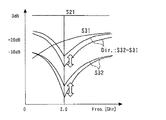
無線端末では送信電力レベルなどのモニターに方向性結合器が用いられることが一般的である。方向性結合器の典型的な構成を図36に示す。図36に示されるように主線路500は送信電力を伝送する線路であり入力ポート(#1)と出力ポート(#2)とに接続される。一方、結合線路502は主線路500の送信電力の一部を取り出すために設けられる線路であり、結合ポート(#3)とアイソレーションポート(#4)とに接続される。なお、方向性結合器は、小型化のためにスパイラル形状で形成される場合もある(図37参照)。方向性結合器の性能は結合量/アイソレーションで定義される方向性と呼ばれる値で表現される。方向性の値が大きいほど、出力ポートからの反射波の影響を抑制して、入力ポートから出力ポートへの送信電力を取り出せることを意味する。前述の結合量およびアイソレーションは周波数依存性を有することが多く、その一例として図38を示す。Dirとは方向性のことである。
In a wireless terminal, a directional coupler is generally used for monitoring the transmission power level and the like. A typical configuration of the directional coupler is shown in FIG. As shown in FIG. 36, the
方向性結合器は例えば送信電力増幅器とアンテナの間に挿入される。前述の方向性結合器は例えば図39に記載の携帯電話端末として用いられる。図39でBB-LSIとは音声やデータを外部とやり取りし、携帯電話端末の信号処理を担う心臓部分である。また、図39でRF/IF-ICとはBB-LSIからの送信用信号を高周波へ周波数変換し増幅器(PA)へ送り、アンテナ(ANT)で受けた信号を中間周波数に変換しBB-LSIへ送るICである。送信用信号の伝送経路上に方向性結合器(Directional coupler)が配置され、その方向性結合器の結合ポートに取り出された信号がキャパシタ(Cc)を介して接続されたディテクタ(DET)へ送られる。結合ポートで取り出された信号はディテクタからBB-LSIへ伝送され、増幅器の出力レベルの監視および制御の指標とされる。 The directional coupler is inserted, for example, between the transmission power amplifier and the antenna. The above-described directional coupler is used as, for example, a mobile phone terminal shown in FIG. In FIG. 39, BB-LSI is a heart that exchanges voice and data with the outside and performs signal processing of the mobile phone terminal. Further, in FIG. 39, RF / IF-IC is a signal for transmission from BB-LSI converted to a high frequency and sent to an amplifier (PA), and a signal received by an antenna (ANT) is converted to an intermediate frequency to convert to BB-LSI. IC to send to. A directional coupler is arranged on the transmission path of the transmission signal, and a signal taken out to the coupling port of the directional coupler is sent to a detector (DET) connected via a capacitor (Cc). It is done. The signal taken out at the coupling port is transmitted from the detector to the BB-LSI and used as an index for monitoring and controlling the output level of the amplifier.
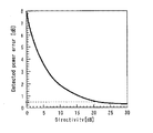
このように、方向性結合器は増幅器の出力レベル(出力電力)のモニターを目的とするため、結合ポートから取り出される信号は増幅器の出力レベルを正確に反映でき、誤差無く高精度であることが望ましい。図40にはディテクタで検出する電力の誤差と方向性結合器の方向性の関係を表すグラフを示す。一般に方向性結合器は0.5dB以下の検出誤差とするために、20dB程度の方向性を有することが求められる。 Since the directional coupler is intended to monitor the output level (output power) of the amplifier, the signal taken out from the coupling port can accurately reflect the output level of the amplifier and must be highly accurate without error. desirable. FIG. 40 is a graph showing the relationship between the power error detected by the detector and the directionality of the directional coupler. In general, the directional coupler is required to have a directivity of about 20 dB in order to obtain a detection error of 0.5 dB or less.
例えば、特許文献1には方向性を高めた方向性結合器が開示されている。すなわち、合成器と呼ばれる装置において送信波の中に含まれる反射波の多重反射分を移相器により位相調整した反射波で打ち消すことで方向性を高める構成が開示されている。
For example,
特許文献1の構成では方向性結合器の小型化(回路寸法の縮小)の要求を満たすことができないという問題があった。また、主線路と結合線路の結合長を使用周波数のλ/4波長とすることによって方向性の改善を図ることも考えられる。しかしながら、例えば携帯端末で使用するような低い周波数帯(0.8〜5GHz帯)では前述のλ/4の値が大きくなり主線路と結合線路の結合長をλ/4の長さとしようとすると、小型化の要求を満たせない問題があった。また、前述の周波数帯(0.8〜5GHz帯)以外の使用周波数であっても諸特性改善のためにGaAs基板などの比較的高価な基板を用いた場合などには、製造コスト低減の観点から方向性結合器の小型化の要求が高い。その結果、前述のλ/4の結合長を満たすことができず十分な方向性を得られない問題があった。
The configuration of
本発明は、上述のような課題を解決するためになされたもので、主線路と結合線路の結合長が使用周波数のλ/4未満である小型化された方向性結合器について、良好な方向性を実現できる方向性結合器を提供することを目的とする。 The present invention has been made in order to solve the above-described problems, and has a good direction for a miniaturized directional coupler in which the coupling length of the main line and the coupling line is less than λ / 4 of the operating frequency. An object of the present invention is to provide a directional coupler capable of realizing the characteristics.
本願の発明にかかる方向性結合器は、基板上に形成され、一端が入力ポートと接続され他端が出力ポートと接続された主線路と、該基板上に該主線路に沿って形成され、該入力ポートと同一方向の一端が結合ポートと接続され、該出力ポートと同一方向の他端がアイソレーションポートと接続された結合線路と、一端が該アイソレーションポートと接続され、他端が該結合ポートと接続された移相器とを備える。そして、該主線路と該結合線路との結合長は、該入力ポートから該出力ポートへの送信電力の使用周波数の1/4波長未満の長さであり、該移相器は、該出力ポートから該結合線路を経由して該結合ポートへ達する反射波成分である第1反射波成分に対して、該出力ポートから該アイソレーションポートおよび該移相器を経由して該結合ポートへ達する反射波成分である第2反射波成分が逆相となるように該第2反射波成分を移相することを特徴とする。 The directional coupler according to the invention of the present application is formed on a substrate, formed on the substrate along the main line, one main line connected to the input port and the other end connected to the output port, One end in the same direction as the input port is connected to a coupling port, the other end in the same direction as the output port is connected to an isolation port, one end is connected to the isolation port, and the other end is connected to the isolation port. A phase shifter connected to the coupling port. The coupling length between the main line and the coupling line is less than ¼ wavelength of the use frequency of the transmission power from the input port to the output port, and the phase shifter includes the output port Reflection from the output port to the coupling port via the isolation port and the phase shifter with respect to the first reflected wave component that is a reflected wave component reaching the coupling port from the output line The second reflected wave component is phase-shifted so that the second reflected wave component, which is a wave component, is in reverse phase.
本発明により小型化され、しかも良好な方向性を有する方向性結合器を製造できる。 According to the present invention, it is possible to manufacture a directional coupler that is miniaturized and has good directivity.
実施の形態1
本実施形態は図1〜図10を参照して説明する。なお、同一材料または同一、対応する構成要素には同一の符号を付して複数回の説明を省略する場合がある。他の実施形態についても同様である。
This embodiment will be described with reference to FIGS. In some cases, the same material or the same and corresponding components are denoted by the same reference numerals, and description thereof is omitted a plurality of times. The same applies to other embodiments.
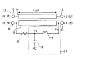
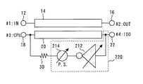
図1は本実施形態の方向性結合器を説明する図である。本実施形態および他の実施形態の方向性結合器は疎結合/側結合型の方向性結合器である。本実施形態の方向性結合器10は基板上に形成された主線路14を備える。主線路14は一端が入力ポート12と接続され他端が出力ポート16と接続される。主線路14は入力ポート12から出力ポート16への送信電力(前進波)を伝送する線路である。基板上には前述の主線路14と沿って結合線路20が形成される。結合線路20は一端が結合ポート18と接続され他端がアイソレーションポート22と接続される。結合線路20は主線路14の送信電力の一部を結合ポートから取り出すための線路である。
FIG. 1 is a diagram illustrating a directional coupler according to this embodiment. The directional couplers of this embodiment and other embodiments are loosely coupled / side coupled directional couplers. The
図1から把握されるように入力ポート12と結合ポート18とは同一方向に配置される。また、出力ポート16とアイソレーションポート22とは同一方向に配置される。ここで、図1においてLcplで表される長さは主線路14と結合線路20の結合長である。本実施形態の方向性結合器10の主線路を伝送する送信電力の使用周波数から求まる波長をλとすると、前述のLcplはλ/4の1/10〜1/20程度まで短いものである。
As can be seen from FIG. 1, the
さらに本実施形態の方向性結合器10は一端がアイソレーションポート22と接続され、他端が抵抗30を介して結合ポート18と接続された移相器24を備える。後述するとおり、移相器24は出力ポート16からの反射波の位相を概ね反転させて結合ポート18へ伝送する部分である。移相器24はインダクタ26とキャパシタ28を備える。インダクタ26は一端がアイソレーションポート22と接続され、他端が抵抗30を介して結合ポート18と接続される。キャパシタ28は一端がインダクタ26の他端と接続され他端が接地される。本実施形態の方向性結合器10は上述の構成を備える。
Furthermore, the
移相器24は出力ポート16から結合線路20を経由して結合ポート18へ達する反射波成分である第1反射波成分に対して、出力ポート16からアイソレーションポート22および移相器24を経由して結合ポート18へ達する反射波成分である第2反射波成分が逆相となるように当該第2反射波成分を移相する。移相は移相器24の共振を利用して行われる。
The
図2は、図1において示されるVa(インダクタの一端における電位)およびVb(キャパシタの一端における電位)の周波数特性を説明する図である。図2におけるfoとは主線路を伝送する送信電力の使用周波数である。また、図2におけるΔfoとは、移相器24の共振点を、第2反射波が第1反射波に対して逆相にできるように調整するためにfoから差し引く値である。すなわち、本実施形態のように結合長(Lcpl)が短い場合はアイソレーションポート22と結合ポート18との間には5から10°程度の位相差が生じる。そこで、前述の逆相合成を行おうと考えた場合にはこの位相差を考慮して移相器24の共振周波数を定める必要がある。Δfoとはこのように定められるものであり、ここでは5から10°である。
FIG. 2 is a diagram for explaining the frequency characteristics of Va (potential at one end of the inductor) and Vb (potential at one end of the capacitor) shown in FIG. Fo in FIG. 2 is a use frequency of transmission power transmitted through the main line. In addition, Δfo in FIG. 2 is a value that is subtracted from fo in order to adjust the resonance point of the
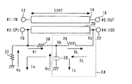
図3〜7を参照して第2反射波を第1反射波に対して略逆相とすることについて説明する。図3は本実施形態の方向性結合器の各部分における電流値及び電圧値に名称を付する図である。図3の構成要素は図1に記載の方向性結合器10とほぼ一致するが、図3においては結合ポート18に設けられる終端抵抗31(50Ω程度)が表されている点において異なる。
With reference to FIGS. 3 to 7, description will be given of making the second reflected wave substantially out of phase with the first reflected wave. FIG. 3 is a diagram in which names are assigned to current values and voltage values in respective portions of the directional coupler of the present embodiment. 3 substantially coincides with the
図4〜図7は図3で名称が付与された電流値及び電圧値のベクトル図である。図4、図5はアイソレーションポート22における電圧Vaと移相器24を介した出力電圧Voは略逆相であることを表す図である。Voは前述した第2反射波成分に対応する。
4 to 7 are vector diagrams of current values and voltage values to which names are given in FIG. 4 and 5 are diagrams showing that the voltage Va at the
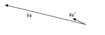
図6は移相器24がない場合のVaと、移相器を介さずに結合ポート18へ達する電圧成分Vo′の関係を表す図である。Vo′は前述した第1反射波成分に対応する。既に述べたとおり、VaとVo′とは5から10°程度の位相差がある。
FIG. 6 is a diagram showing the relationship between Va when there is no
図7は図5、6を合成した図である。図7からVoとVo′は略逆相であることが分かる。このように、移相器24の回路定数を調整することでVo′(第2反射波成分)をVoに対して略逆相合成できる。さらに、方向性結合器の方向性を高めるためにはVoとVo′が等振幅であることが好ましい。本実施形態の抵抗30は前述のVoとVo′が等振幅となるようにVbを減衰させる。すなわち、図7のベクトル図から明らかなように、Vo′はキャパシタ28の一端における電圧Vbから抵抗30の電圧Vrを差し引いた値である。これにより、図7に示されるように、VoとVo′が相殺されるように両者を等振幅とすることができる。
FIG. 7 is a combination of FIGS. It can be seen from FIG. 7 that Vo and Vo ′ are substantially in reverse phase. In this way, by adjusting the circuit constant of the
一般に方向性結合器の性能は結合量、アイソレーション特性、方向性で定義される。結合量とは入力ポート12と結合ポート18との結合の度合いを表す。結合量は結合ポート18における信号電力を入力ポート12における信号電力で除算した値であり、−10〜−20dB程度であることが多い。アイソレーション特性は出力ポート16からの反射波と結合ポート18との結合の強さを表す。アイソレーション特性は出力ポート16からの反射波で結合ポート18に表れる信号電力を前述の反射波の電力で除算したものである。アイソレーション特性は通常−15〜−30dB程度であることが多い。方向性は結合量をアイソレーション特性で除算した値である。
In general, the performance of a directional coupler is defined by the amount of coupling, isolation characteristics, and directionality. The coupling amount represents the degree of coupling between the
方向性の値が大きいほど、出力ポート16からの反射波の影響を低減して送信電力の検出ができるため、方向性結合器の検出誤差が小さくなる。すなわち、負荷変動時においても検波回路で送信電力(前進波電力)を正確にモニタできる。その結果、検波電圧に含まれる反射波による誤差が抑制され、負荷変動時に増幅器(PA)からの過大電力送信に伴う歪み成分を抑制できる。
As the directional value is larger, the influence of the reflected wave from the
しかしながら、方向性結合器の小型化の要請に応じて前述の主線路と結合線路の結合長をλ/4より短くした場合には方向性が悪化する問題があった。 However, when the coupling length between the main line and the coupling line is made shorter than λ / 4 in response to a request for downsizing of the directional coupler, there is a problem that the directivity deteriorates.
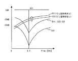
本実施形態の構成によれば結合長がλ/4より短い場合であっても方向性を高めることができる。図8は本実施形態の方向性結合器の諸特性についての周波数特性を説明するグラフである。図8においてS31は結合量の周波数特性を、S32はアイソレーション特性の周波数特性を、S32‐S31は方向性の周波数特性を表す。前述の通り移相器24が第2反射波を第1反射波に対して略逆相となるように移相するため、S32が良好(デシベル値が高い)な領域を得ることができる。従って、この実施形態ではアイソレーション(S32)が良好な領域である2GHz周辺においては30dB程度の高い方向性を有する方向性結合器を得ることができる。
According to the configuration of the present embodiment, the directionality can be improved even when the coupling length is shorter than λ / 4. FIG. 8 is a graph for explaining frequency characteristics of various characteristics of the directional coupler of this embodiment. In FIG. 8, S31 represents the frequency characteristic of the coupling amount, S32 represents the frequency characteristic of the isolation characteristic, and S32-S31 represent the directional frequency characteristic. As described above, since the
本実施形態の方向性結合器は、2GHz周辺で高い方向性を有するので無線通信などの狭帯域通信を目的とする機器への応用に適している。本実施形態の方向性結合器は様々な変形が可能である。図9、10を参照して本実施形態の方向性結合器の変形例について説明する。 Since the directional coupler of this embodiment has high directivity around 2 GHz, it is suitable for application to equipment for narrowband communication such as wireless communication. Various modifications can be made to the directional coupler of this embodiment. A modification of the directional coupler of this embodiment will be described with reference to FIGS.
図9は、2つの方向の異なる移相器を備える方向性結合器である。図9の方向性結合器は入力ポート、出力ポートを逆転させて双方向に使用できることが特徴である。第1移相器40の一端には第1トランジスタ51を介してアイソレーションポート54が接続され、他端には抵抗44および第2トランジスタ48を介して結合ポート50が接続される。第2移相器42の一端には第3トランジスタ52を介して結合ポート50が接続され、他端には抵抗46および第4トランジスタ55を介してアイソレーションポート54が接続される。入力ポート12から出力ポート16へ送信電力が伝送されている場合には第1トランジスタ51、第2トランジスタ48をオンとして第3トランジスタ52、第4トランジスタ55をオフとする。一方出力ポート16から入力ポート12へ送信電力が伝送されている場合には第1トランジスタ51、第2トランジスタ48をオフとして第3トランジスタ52、第4トランジスタ55をオンとする。このように制御することで、双方向の送信電力の伝送に対応した方向性結合器であっても、移相器を備えることによる本実施形態の効果を得ることができる。なお、第1移相器40、第2移相器42の構成については本実施形態で説明した移相器24と同様であるから詳細な説明を省略する。
FIG. 9 is a directional coupler including phase shifters having two different directions. The directional coupler of FIG. 9 is characterized in that the input port and the output port can be reversed and used in both directions. An
図10は設計の容易性を高めた方向性結合器である。図10に示す方向性結合器が備える移相器60は機能としては上述した図1における移相器24と同等である。しかしながら移相器60は第1インダクタ62および第1キャパシタ64からなる第1移相部と第2インダクタ66および第2キャパシタ68からなる第2移相部とからなる。通常、LC回路は90°の移相に用いることが多く、この場合設計も容易である。さらに、良好な方向性を有する帯域を広くすることもできる。
FIG. 10 shows a directional coupler with improved design ease. The
その他、本実施形態の方向性結合器は様々な変形が可能である。例えば、本実施形態では30dB程度の高い方向性を有する周波数を20GHz近傍としたが、この値は図2で説明した移相器24の回路定数(共振周波数)の設定によって任意に変えることができる。また、抵抗30は図7で説明したVoとVo′を等振幅とするために設けられる。よって、抵抗30なしにVoとVo′がほぼ等振幅あるいは振幅差が微小であれば、抵抗30を設けなくても良い。また、結合長は使用周波数λの場合にλ/4未満であれば、方向性の低下の問題が生じ本実施形態の効果による方向性の改善が図れるため、結合長はλ/4未満であれば限定されない。
In addition, the directional coupler of this embodiment can be variously modified. For example, in this embodiment, the frequency having a high directivity of about 30 dB is set to around 20 GHz, but this value can be arbitrarily changed by setting the circuit constant (resonance frequency) of the
実施の形態2
本実施形態は移相器の備えるキャパシタを可変容量キャパシタとした方向性結合器に関するものである。本実施形態は図11〜図13を参照して説明する。本実施形態の方向性結合器は実施形態1の構成とほぼ同等であるが、移相器の構成が異なる。以後図11に示す移相器80を説明する。
The present embodiment relates to a directional coupler in which a capacitor provided in a phase shifter is a variable capacitor. This embodiment will be described with reference to FIGS. The directional coupler of the present embodiment is almost the same as the configuration of the first embodiment, but the configuration of the phase shifter is different. Hereinafter, the
移相器80は、一端においてインダクタ26の他端と接続され、他端は接地されたキャパシタ82を備える。さらに、一端においてキャパシタ82の一端と接続され、他端は後述のダイオード86と接続されたキャパシタ84を備える。さらに、アノードが接地され、カソードがキャパシタ84の他端と接続されたダイオード86を備える。ダイオード86のカソードには抵抗88を介して制御電圧Vcの供給源が接続されている。
The
方向性結合器の部品としてのダイオード86は、抵抗と可変容量キャパシタとみなすことができる。本実施形態では制御電圧Vcを変化させることでダイオード86を可変容量キャパシタとして利用する。そして、容量を変化させることで移相器80の共振周波数を変化させることができる。すなわち、制御電圧Vcを変化させることによって高い方向性を有する周波数帯域をシフトさせることができる。
The
図12は図11で説明した方向性結合器の諸特性の周波数特性を説明するグラフである。制御電圧Vcの印加により容量を変化させることで移相器の共振周波数を変化させることができるから、図12に矢印で示されるように良好な方向性を有する周波数帯を変化させることができる。このような方向性結合器はマルチバンド(複数の異なる使用周波数)で用いる方向性結合器などに特に有効である。制御電圧Vcをダイオード86のカソードに印加する制御電圧印加手段は方向性結合器の外部であって主線路の送信電力の周波数を定める部分と接続され、送信電力の周波数に応じて方向性を最適化するようにVcを定めることとしても良い。図11では制御電圧印加手段を単にVcで表されるポートで表現する。
FIG. 12 is a graph illustrating frequency characteristics of various characteristics of the directional coupler described in FIG. Since the resonance frequency of the phase shifter can be changed by changing the capacitance by applying the control voltage Vc, it is possible to change the frequency band having good directivity as shown by the arrows in FIG. Such a directional coupler is particularly effective for a directional coupler used in a multiband (a plurality of different used frequencies). The control voltage applying means for applying the control voltage Vc to the cathode of the
この実施形態の可変容量キャパシタは図11の構成に限定されない。すなわち、本実施形態は使用周波数に応じて高い方向性を得られるように移相器の容量を可変とすることが特徴である。よって、回路図としては図13に示すように可変容量キャパシタ90が存する限りにおいて本実施形態の効果を失わない。
The variable capacitor of this embodiment is not limited to the configuration of FIG. That is, this embodiment is characterized in that the capacity of the phase shifter is variable so that high directionality can be obtained according to the operating frequency. Therefore, as long as the
実施の形態3
本実施形態は移相器の備えるインダクタを可変インダクタとした方向性結合器に関するものである。本実施形態は図14〜図16を参照して説明する。本実施形態の方向性結合器は実施形態1の構成とほぼ同等であるが、移相器の構成が異なる。以後図14に示す移相器106を説明する。
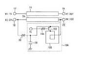
The present embodiment relates to a directional coupler in which an inductor included in a phase shifter is a variable inductor. This embodiment will be described with reference to FIGS. The directional coupler of the present embodiment is almost the same as the configuration of the first embodiment, but the configuration of the phase shifter is different. Hereinafter, the
実施形態3のインダクタ100はスパイラル形状の線路を備える。さらに、インダクタ100の線路における2点をソースドレインで接続するトランジスタ102を備える。トランジスタ102はFETであるがこれに限定されない。トランジスタ102のゲートは制御電圧Vcにより制御される。このような構成とすると制御電圧Vcを制御することでインダクタ100のインダクタンスを変化させることができる。よって実施形態2と同様に良好な方向性を得られる周波数帯を変動させることができる。制御電圧印加手段を用いてマルチバンドに対応することなどは実施形態2と同様なので説明を省略する。なお、トランジスタ102と異なるトランジスタをインダクタと接続してさらに複数の周波数帯での使用を可能にすることが可能である。本実施形態の最も一般化された回路図を図15に示す。このようにインダクタンスの値を可変とすることが本実施形態の特徴である。よって、インダクタは反転位相が取り出せるトランス110で構成しても良い(図16)。
The
実施の形態4
本実施形態は移相器の他端と接続された抵抗を可変抵抗とした方向性結合器に関するものである。本実施形態は図17〜図19を参照して説明する。本実施形態の方向性結合器は実施形態1の構成とほぼ同等であるが、抵抗の構成が異なる。以後図17に示す抵抗120を説明する。
This embodiment relates to a directional coupler in which a resistance connected to the other end of the phase shifter is a variable resistance. This embodiment will be described with reference to FIGS. The directional coupler of the present embodiment is almost the same as the configuration of the first embodiment, but the resistance configuration is different. Hereinafter, the
抵抗120は移相器24の他端と結合ポート18とを接続するトランジスタ126を備える。トランジスタ126のチャネル抵抗は、FETであるトランジスタ126のゲートに印加される制御電圧Vcにより制御される。制御電圧Vcを変化させることで方向性等の周波数特性を表す図18において矢印で示されるように方向性を変化させることができる。図17から明らかであるがトランジスタ126と並列に接続された抵抗122はトランジスタ126がオフのときに第2反射波成分を結合ポート18へ伝送するために配置される。なお、本実施形態の方向性結合器を一般化した図は図19に示す。
The
このように抵抗値を可変とすることにより、方向性結合器の製造後に第1反射波と第2反射波を等振幅となるように抵抗値を最適化したり、製造ばらつきにより第1反射波と第2反射波とが等振幅とならなかった場合にそれを是正するように抵抗値を最適化したりできる。 By making the resistance value variable in this way, the resistance value is optimized so that the first reflected wave and the second reflected wave have the same amplitude after the directional coupler is manufactured, If the second reflected wave does not have the same amplitude, the resistance value can be optimized so as to correct it.
実施の形態5
本実施形態は複数の異なる使用周波数を用いる方向性結合器の結合量を可変化した方向性結合器に関するものである。本実施形態は図20、21を参照して説明する。本実施形態の方向性結合器は実施形態1の構成とほぼ同等であるが、主線路14と結合線路20とが第1電界効果トランジスタ130のソースドレインおよび第2電界効果トランジスタ132のソースドレインで接続されている点が異なる。また、移相器134が可変容量キャパシタ90を備える点も異なる。
This embodiment relates to a directional coupler in which the coupling amount of a directional coupler using a plurality of different use frequencies is made variable. This embodiment will be described with reference to FIGS. The directional coupler of the present embodiment is almost the same as the configuration of the first embodiment, but the
第1電界効果トランジスタ130と第2電界効果トランジスタ132のゲートをそれぞれ制御するために制御電圧Vc1、 Vc2を印加する手段が設けられている。本実施形態の方向性結合器はVc1、Vc2を制御し第1電界効果トランジスタ130と第2電界効果トランジスタ132の可変容量特性を利用して結合量を変化させることができる。具体的には複数の異なる使用周波数間でも結合量が一定となるようにVc1とVc2が制御される。
Means for applying control voltages Vc1 and Vc2 are provided to control the gates of the first
本実施形態の方向性結合器の制御例を図21に示す。図21ではBand1とBand2の両方の周波数を用いる場合を想定している。第1電界効果トランジスタ130(図21ではF1)と第2電界効果トランジスタ132(図21ではF2)は次のように制御される。つまり、Band1を用いる場合にはF1をオン、F2をオフとし、Band2を用いる場合にはその逆の制御を行う。このような制御によりBand1-Band2間で結合量を一定とし得る。 An example of control of the directional coupler of this embodiment is shown in FIG. FIG. 21 assumes a case where both Band1 and Band2 frequencies are used. The first field effect transistor 130 (F1 in FIG. 21) and the second field effect transistor 132 (F2 in FIG. 21) are controlled as follows. That is, when using Band1, F1 is turned on and F2 is turned off, and when Band2 is used, the opposite control is performed. By such control, the amount of coupling between Band1 and Band2 can be made constant.
一般に、本実施形態のように複数の異なる使用周波数を用いる場合は、異なる周波数間で結合量を一定とすることが好ましい。例えば、ある周波数で結合量が高くなると結合ポートへの出力が増え、アンテナへの出力が減るため好ましくない。よって結合量が高いことは方向性を改善することに寄与するものの、損失が増大する問題もあるため一定水準以下とすることが好ましい。また、結合ポートからの出力を検出するディテクタもほぼ一定の電圧に対応するものであるため、使用周波数によって結合量が大きく変化することは好ましくない。本実施形態のように結合量を可変とし、使用周波数に応じて結合量を一定とする制御を行うことで上述の問題を解決できる。 In general, when a plurality of different use frequencies are used as in the present embodiment, it is preferable to make the coupling amount constant between different frequencies. For example, an increase in the amount of coupling at a certain frequency is not preferable because the output to the coupling port increases and the output to the antenna decreases. Therefore, although a high amount of coupling contributes to improving the directionality, there is a problem that the loss increases, so it is preferable to set the level below a certain level. Further, since the detector for detecting the output from the coupling port also corresponds to a substantially constant voltage, it is not preferable that the coupling amount varies greatly depending on the operating frequency. The above-described problem can be solved by controlling the amount of coupling to be variable and the amount of coupling to be constant according to the operating frequency as in this embodiment.
また、例えば第1または第2電界効果トランジスタのドレイン−ソース間容量を増大させて結合量を20dBから15dBへ増大させた場合は、アイソレーション特性が悪化するため方向性の著しい劣化を伴うものである。しかしながら本実施形態では移相器134が可変容量キャパシタ90を備えているため、複数の帯域に渡って前述の劣化を補うように方向性を改善できる。
Further, for example, when the drain-source capacitance of the first or second field effect transistor is increased to increase the coupling amount from 20 dB to 15 dB, the isolation characteristic is deteriorated and the directivity is significantly deteriorated. is there. However, in this embodiment, since the
本実施形態では電界効果トランジスタを2つ用いる構成としたが、電界効果トランジスタの数が1つの場合であっても3以上の場合であってもこの実施形態の効果を得ることができる。 In this embodiment, two field effect transistors are used, but the effect of this embodiment can be obtained regardless of whether the number of field effect transistors is one or three or more.
実施の形態6
本実施形態は少なくとも低域バンドと低域バンドよりも周波数の高い高域バンドで使用する方向性結合器の結合長を可変化した方向性結合器に関するものである。本実施形態は図22を参照して説明する。本実施形態の方向性結合器は実施形態1の構成とほぼ同等である。しかしながら、結合線路が第1スイッチング素子140のソースドレインを介して接続された第1結合線路142と第2結合線路144とに分割されている点が異なる。また、移相器134のキャパシタは可変容量キャパシタ90である。
The present embodiment relates to a directional coupler in which the coupling length of a directional coupler used at least in a low frequency band and a high frequency band having a frequency higher than that of the low frequency band is made variable. This embodiment will be described with reference to FIG. The directional coupler of the present embodiment is almost the same as the configuration of the first embodiment. However, the difference is that the coupled line is divided into a first coupled
第1結合線路142の一端はアイソレーションポート22と接続され他端は第1スイッチング素子140の一端と接続される。第2結合線路144第1の一端は第1スイッチング素子140の他端と接続され、他端は結合ポート18と接続される。そして移相器134の一端と第2結合線路144の一端とは第2スイッチング素子146を介して接続される。
One end of the
本実施形態の構成は上述の通りである。実施形態5で述べたとおり、方向性結合器の結合量は複数帯域間で同等であることが好ましい。本実施形態のように少なくとも低域バンドと高域バンドでの使用を前提とした場合には結合長そのものを切り替えることにより低域バンド高域バンド間で結合量を一定とすることができる。本実施形態では低域バンドで方向性結合器を用いる場合には第1スイッチング素子140をオン、第2スイッチング素子146をオフとする。高域バンドで用いる場合には第1スイッチング素子140をオフ、第2スイッチング素子146をオンとする。第1結合線路142と第2結合線路144の線路長は前述した使用状況において低域バンド、高域バンド間で結合量を一定にできるように定められるため実施形態5と同様に結合量を一定とする効果を得ることができる。
The configuration of this embodiment is as described above. As described in the fifth embodiment, it is preferable that the coupling amount of the directional coupler is equal between a plurality of bands. Assuming the use in at least a low band and a high band as in the present embodiment, the coupling amount can be made constant between the low band and the high band by switching the coupling length itself. In the present embodiment, when the directional coupler is used in the low band, the
上述のように複数の使用周波数間で結合量を一定とする制御は、第1スイッチング素子140と第2スイッチング素子143のゲートにそれぞれVcとVcの反転を入力する。図22ではVcおよびVcの反転の制御手段として第1スイッチング素子140のゲートと第2スイッチング素子146のゲートに接続されたポートを示す。
As described above, in order to make the amount of coupling constant among a plurality of operating frequencies, inversion of Vc and Vc is input to the gates of the
実施の形態7
本実施形態は移相器にアクティブ素子である位相反転増幅器を用いた方向性結合器に関する。本実施形態は図23〜28を参照して説明する。本実施形態の方向性結合器は実施形態1の構成とほぼ同等である。しかしながら、移相器が位相反転増幅器を備える点が異なる。図23は本実施形態の方向性結合器を説明する図である。本実施形態の移相器は実施形態1〜6と異なり、アクティブ素子である位相反転増幅器202を用いることが特徴である。本実施形態の位相反転増幅器202は入力信号を増幅させるのではなく減衰させて結合ポートへ伝送するものである。
Embodiment 7
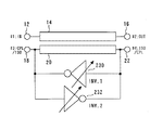
The present embodiment relates to a directional coupler using a phase inverting amplifier as an active element for a phase shifter. This embodiment will be described with reference to FIGS. The directional coupler of the present embodiment is almost the same as the configuration of the first embodiment. However, the difference is that the phase shifter comprises a phase inverting amplifier. FIG. 23 is a diagram illustrating the directional coupler according to the present embodiment. Unlike the first to sixth embodiments, the phase shifter of the present embodiment is characterized by using a
一般に位相反転増幅器は広帯域に渡って位相反転を得ることができる。そのため、本実施形態の移相器200もここまでの実施形態の移相器と同様に第2反射波成分を第1反射波成分に対して逆相となるように第2反射波成分を移相できる。移相器として増幅器を用いる場合には、過入力となったときに信号が歪みやすい点に留意して、信号歪の起こらないように設計する必要がある。しかしながら、方向性結合器を送信モジュールに組み込む場合、位相反転増幅器202は方向性結合器の前段に配置される増幅器(PA)と比較して遥かに小さい電流で動作するものである。従って位相反転増幅器の電流消費そのものがモジュール特性を損なう可能性は低い。
In general, a phase inverting amplifier can obtain phase inversion over a wide band. Therefore, the
本実施形態のように移相器として位相反転増幅器202を用いることは移相器の回路寸法の小型化に有利である。すなわち位相反転増幅器202は一般にトランジスタと抵抗により構成されるため、インダクタとキャパシタを用いる実施形態1〜6の構成と比較して小型化できる。
Using the
図24は本実施形態の変形例について説明する図である。図24に示す方向性結合器は利得が可変である位相反転増幅器212を備える。利得を可変とすることで、第1反射波成分と第2反射波成分とが等振幅となるように第2反射波成分を減衰させることができるため、実施の形態4の構成と同様の効果を簡素な構成で得ることができる。
FIG. 24 is a diagram for explaining a modification of the present embodiment. The directional coupler shown in FIG. 24 includes a
図25は本実施形態の別の変形例について説明する図であり、特に複数の異なる使用周波数を用いる方向性結合器に関する。図25に示す方向性結合器の移相器220は利得が可変である位相反転増幅器212と可変移相器214を備える。すなわち、移相器220は一端がアイソレーションポート22と接続され他端が可変移相器214の一端と接続された位相反転増幅器212を備える。そして可変移相器214の他端は抵抗30を介して結合ポート18と接続される。可変移相器214は実施形態2で記載したように使用周波数に応じて高い方向性が得られる帯域をシフトさせるように制御されることで実施形態2と同等の効果を得ることができる。
FIG. 25 is a diagram for explaining another modified example of the present embodiment, and particularly relates to a directional coupler using a plurality of different use frequencies.
図26は位相反転増幅器212の構成を説明する回路図である。図26においてTr1とTrREFはHBT(ヘテロ接合バイポーラトランジスタ)である。F1はFET(電界効果トランジスタ)である。またRc1は負荷抵抗である。RFB1、RFB2、CFB1はTr1のベースコレクタ間に設けたフィードバック回路である。前述の通り位相反転増幅器212は減衰特性を有する可変利得回路であるので、フィードバック回路を設けることで帯域を広げると共に利得を低減することができる。フィードバック回路のFETであるF1のゲート電圧VGC1を制御することで、F1のON抵抗を制御できるので、フィードバック量を制御できため利得を制御できる。なお、RIN1、RO1は位相反転増幅器212の利得減衰用の抵抗である。これらの抵抗値を適当な値とすることで方向性を高めるように減衰特性を設定できる。
FIG. 26 is a circuit diagram illustrating the configuration of the
ここで、Tr1とTrREFはカレントミラー回路を構成する。Tr1のバイアス電流はVREFで調整できる。Tr1のコンダクタンス(gm) はこのバイアス電流に比例するため、バイアス電流を制御することで利得量(減衰量)を調整できる。 Here, Tr1 and TrREF constitute a current mirror circuit. The bias current of Tr1 can be adjusted by VREF . Since the conductance (gm) of Tr 1 is proportional to this bias current, the amount of gain (attenuation) can be adjusted by controlling the bias current.
図27は図25における可変移相器214の構成を説明する図である。図27の構成は実施形態1において図10を参照して説明した構成と比較してキャパシタが可変容量キャパシタである点が相違している。このように可変移相器214の備えるキャパシタを可変容量化することおよびその効果は実施形態2で記載したものと同様である。
FIG. 27 is a diagram for explaining the configuration of the
図28は本実施形態の別の変形例を説明する図である。図28には双方向の送信電力の伝送に対応した方向性結合器であっても、高い方向性を得ることができる方向性結合器が記載されている。図28に記載の方向性結合器は移相器として、利得が可変である位相反転増幅器230と利得が可変である位相反転増幅器232とを備えることが特徴である。この構成は、実施形態1において図9を参照して説明済みである方向性結合器の移相器をアクティブ素子に置き換えた構成である。従ってアクティブ素子を用いた簡素な構成で図9の構成と同等の効果を得ることができる。
FIG. 28 is a diagram for explaining another modification of the present embodiment. FIG. 28 shows a directional coupler that can obtain high directionality even if it is a directional coupler that supports transmission of bidirectional transmission power. The directional coupler shown in FIG. 28 is characterized by including a
実施の形態8
本実施形態は少なくとも低域バンドと低域バンドよりも周波数の高い高域バンドで使用する方向性結合器であって使用周波数が異なっても結合量を一定にできる方向性結合器に関する。本実施形態は図29、30を用いて説明する。
Embodiment 8
The present embodiment relates to a directional coupler that is used in at least a low-frequency band and a high-frequency band having a frequency higher than that of the low-frequency band, and that can keep the amount of coupling constant even when the used frequency is different. This embodiment will be described with reference to FIGS.
図29は本実施形態の方向性結合器を説明する図である。本実施形態の方向性結合器は使用周波数に応じて結合線路を使い分ける構成である。図29から把握されるように入力ポート12と出力ポート16に接続された主線路14は、主線路14に沿った高域バンド用結合線路300と低域バンド用結合線路302に挟まれるように配置される。
FIG. 29 is a diagram illustrating the directional coupler according to the present embodiment. The directional coupler of the present embodiment has a configuration in which the coupling line is properly used according to the operating frequency. As can be understood from FIG. 29, the
低域バンド用結合線路302の一端は第1スイッチング素子312を介して結合ポート18と接続される。低域バンド用結合線路302の他端は第3スイッチング素子314を介して第1アイソレーションポート317と接続される。一方、高域バンド用結合線路300の一端は第2スイッチング素子308を介して結合ポート18と接続される。高域バンド用結合線路300の他端は第4スイッチング素子310を介して第2アイソレーションポート315と接続される。
One end of the low
さらに、低域バンド用結合線路302の両端には第1移相器306および抵抗318が低域バンド用結合線路302と並列に接続される。高域バンド用結合線路300の両端には第2移相器304および抵抗316が高域バンド用結合線路300と並列に接続される。第1移相器306、第2移相器304は共に可変容量キャパシタを備える移相器でありこの構成については実施形態2で説明済みである。
Further, a
本実施形態の方向性結合器は、低域バンドを用いる場合には第1スイッチング素子312、第3スイッチング素子314をオン、第2スイッチング素子308、第4スイッチング素子310をオフとする。また、高域バンドを用いる場合には第1スイッチング素子312、第3スイッチング素子314をオフとし、第2スイッチング素子308、第4スイッチング素子310をオンとする。このようなオンオフの制御は方向性結合器の内部又は外部に設けられた電圧印加手段が前述したスイッチング素子のスイッチングを行うことにより実施される。本実施形態の方向性結合器では前述のスイッチングを行うための制御手段として各スイッチング素子に対して少なくとも電圧印加用のポート(図29においてVc1、Vc2で示す)を有する。
The directional coupler according to the present embodiment turns on the
主線路14と低域バンド用結合線路302との間の距離は、主線路14と高域バンド用結合線路300の距離より短い。すなわち、低域バンド使用時には十分な結合量を得るために主線路14と低域バンド用結合線路302との距離を短くするのに対し、高域バンド使用時には結合量が高くなりすぎることを抑制するために主線路14と高域バンド用結合線路300との距離を大きくする。本実施形態ではこのようにしてどちらの周波数帯を用いた場合であっても方向性結合器の結合量がほぼ一定となるように線路間の距離を調整している。一般に、結合ポートの後段に配置されたディテクタでの検出電力は使用周波数に係らず一定範囲内であることが検出精度の観点から好ましい。本実施形態の構成によれば、複数の周波数を用いる方向性結合器の結合量を一定とできるため、前述の効果を得る。
The distance between the
さらに、低域バンドで用いられる移相器306と高域バンドで用いられる移相器304はそれぞれが高い方向性を有するように共振周波数(回路定数)が定められている。よって図30に記載されるように複数の使用周波数を用いる方向性結合器の方向性を、使用周波数依存なく高めることができる。
Further, the resonance frequency (circuit constant) is determined so that each of the
実施の形態9
本実施形態は少なくとも低域バンドと低域バンドよりも周波数の高い高域バンドで使用する方向性結合器であって使用周波数が異なっても結合量を一定にできる方向性結合器に関する。本実施形態は図31、32を用いて説明する。
Embodiment 9
The present embodiment relates to a directional coupler that is used in at least a low-frequency band and a high-frequency band having a frequency higher than that of the low-frequency band, and that can keep the amount of coupling constant even when the used frequency is different. This embodiment will be described with reference to FIGS.
図31は本実施形態の方向性結合器を説明する図である。本実施形態の方向性結合器は使用周波数に応じて主線路を使い分ける構成である。図31から把握されるように結合ポート18とアイソレーションポート22に接続された結合線路20は、結合線路20に沿った高域バンド用主線路400と低域バンド用主線路402に挟まれるように配置される。
FIG. 31 is a diagram for explaining the directional coupler of this embodiment. The directional coupler of this embodiment is configured to use the main line properly according to the operating frequency. As can be seen from FIG. 31, the coupled
高域バンド用主線路400は一端が高域バンド用入力ポート404と接続され、他端が高域バンド用出力ポート406と接続される。一方低域バンド用主線路402は一端が低域バンド用入力ポート408と接続され、他端が低域バンド用出力ポート410と接続される。
The high band
本実施形態も実施形態1と同様に一端が結合ポート18と他端がアイソレーションポート22と接続された移相器を備える構成であるが、本実施形態の移相器は高域バンド用移相器450と低域バンド用移相器452からなる。高域バンド用移相器450は一端が第3スイッチング素子430を介してアイソレーションポート22と接続され、他端では抵抗30および第1スイッチング素子428を介して結合ポート18と接続される。一方、低域バンド用移相器452は一端が第4スイッチング素子434を介してアイソレーションポート22と接続され、他端では抵抗30および第2スイッチング素子432を介して結合ポート18と接続される。
Similarly to the first embodiment, the present embodiment also includes a phase shifter having one end connected to the
本実施形態の方向性結合器は、低域バンドを用いる場合には第2スイッチング素子432、第4スイッチング素子434をオン、第1スイッチング素子428、第3スイッチング素子430をオフとする。また、高域バンドを用いる場合には第1スイッチング素子428、第3スイッチング素子430をオン、第2スイッチング素子432、第4スイッチング素子434をオフとする。このようなオンオフの制御は方向性結合器の内部又は外部に設けられた電圧印加手段が前述したスイッチング素子のスイッチングを行うことにより実施される。本実施形態の方向性結合器では前述のスイッチングを行うための制御手段として各スイッチング素子に対して少なくとも電圧印加用のポート(図31においてVc1、Vc2で示す)を有する。
The directional coupler according to the present embodiment turns on the
結合線路20と低域バンド用主線路402との間の距離は、結合線路20と高域バンド用主線路400の距離より短い。これは方向性結合器が低域バンド使用時と高域バンド使用時において結合量を一定とするように線路間の距離を調整するものである。さらに、低域バンド用移相器452と高域バンド用移相器450を備えこれらを使用周波数によって使い分けることで、使用周波数によらず高い方向性を得ることができる(図32参照)。よって本実施形態の効果は実施形態8と同様である。本実施形態のように主線路を2本設けることは、方向系結合器の前段にPA(増幅器)が2つ設けられ、出力線路も2本であるGSM(Global-System-for-Mobile-communications)方式の端末(GSM用送信モジュール)などへの応用に適している。
The distance between the coupled
実施の形態10
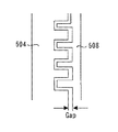
本実施形態は移相器を付加することによる結合量の低下を補うことができる方向性結合器に関する。本実施形態は図33〜35を参照して説明する。図33は本実施形態の方向性結合器を説明する図である。図33に記載の通り、本実施形態の主線路504はスパイラル形状で形成されている。主線路504の一端には入力ポート500、他端には出力ポート502が接続される。スパイラル形状の主線路504に沿って同じくスパイラル形状の結合線路508が形成される。実施形態1と同様に結合線路508の一端には結合ポート506、他端にはアイソレーションポート507が接続される。
The present embodiment relates to a directional coupler that can compensate for a decrease in coupling amount due to the addition of a phase shifter. This embodiment will be described with reference to FIGS. FIG. 33 is a diagram for explaining the directional coupler of the present embodiment. As shown in FIG. 33, the
主線路504と結合線路508はその一部においてくし型に形成される。くし型に形成された部分は図33における破線に示されている。図34は図33における破線部分の拡大図である。図34に示されるように主線路504と結合線路508は相互に嵌りあうようくし型の形状である。また、主線路504と結合線路508とは一定の間隔だけ離間している。
The
さらに本実施形態の方向性結合器は移相器を備える。移相器24は実施形態1と同様の構成であり、一端がアイソレーションポート507と接続され他端が抵抗30を介して結合ポート506と接続される。
Furthermore, the directional coupler of this embodiment includes a phase shifter. The
方向性結合器に移相器24を付加することで結合量が低下し方向性に悪影響を与えることがある。発明者らが行った実験では移相器を付加しない場合の結合量は-20dB程度であった方向性結合器において、移相器を付加すると結合量は-23dB程度まで低下することが見出されている。本実施形態では、主線路504および結合線路508にくし型の部分を設けて電界分布を集中させることで方向性結合器を大型化することなく結合量を高めることができる。また、スパイラル形状の主線路504および結合線路508を形成しているため、方向性結合器を大型化することなしに結合長の延長を図ることができる。よって移相器を付加することによる結合量の低下を抑制し、方向性を良好な値に保つことができる。図35にはくし型の形状の有無による結合量(S31)の差を示す。
By adding the
本実施形態では主線路504と結合線路508とが相対する部分の一部がくし型に形成される構成としたが、主線路504と結合線路508が相対する部分全体において両者をくし型に形成して結合量を高めても良い。他方結合量が十分であるときはくし型に形成される部分をより小さい領域にとどめてもよい。
In the present embodiment, a part of the portion where the
12 入力ポート、 14 主線路、 16 出力ポート、 18 結合ポート、 20 結合線路、 22 アイソレーションポート、 24 移相器、 30 抵抗 12 input ports, 14 main lines, 16 output ports, 18 coupled ports, 20 coupled lines, 22 isolation ports, 24 phase shifters, 30 resistors
Claims (16)
前記基板上に前記主線路に沿って形成され、前記入力ポートと同一方向の一端が結合ポートと接続され、前記出力ポートと同一方向の他端がアイソレーションポートと接続された結合線路と、
一端が前記アイソレーションポートと接続され、他端が前記結合ポートと接続された移相器とを備え、
前記主線路と前記結合線路との結合長は、前記入力ポートから前記出力ポートへの送信電力の使用周波数の1/4波長未満の長さであり、
前記移相器は、前記出力ポートから前記結合線路を経由して前記結合ポートへ達する反射波成分である第1反射波成分に対して、前記出力ポートから前記アイソレーションポートおよび前記移相器を経由して前記結合ポートへ達する反射波成分である第2反射波成分が逆相となるように前記第2反射波成分を移相することを特徴とする方向性結合器。 A main line formed on a substrate, having one end connected to an input port and the other end connected to an output port;
A coupling line formed on the substrate along the main line, one end in the same direction as the input port is connected to a coupling port, and the other end in the same direction as the output port is connected to an isolation port;
A phase shifter having one end connected to the isolation port and the other end connected to the coupling port;
The coupling length between the main line and the coupling line is a length less than a quarter wavelength of the use frequency of transmission power from the input port to the output port,
The phase shifter is configured to change the isolation port and the phase shifter from the output port to a first reflected wave component that is a reflected wave component reaching the coupling port from the output port via the coupling line. A directional coupler in which the second reflected wave component is phase-shifted so that the second reflected wave component, which is a reflected wave component that reaches the coupling port via a reverse phase, is in reverse phase.
一端が前記アイソレーションポートと接続され、他端が前記結合ポートと接続されたインダクタと、
一端が前記インダクタの他端と接続され他端が接地されたキャパシタとを備え、
前記移相器の共振周波数は前記第1反射波成分と前記第2反射波成分とが逆相になるように定められることを特徴とする請求項1に記載の方向性結合器。 The phase shifter is
An inductor having one end connected to the isolation port and the other end connected to the coupling port;
A capacitor having one end connected to the other end of the inductor and the other end grounded;
2. The directional coupler according to claim 1, wherein a resonance frequency of the phase shifter is determined so that the first reflected wave component and the second reflected wave component are in opposite phases.
前記キャパシタは、前記複数の異なる使用周波数に応じて方向性結合器の方向性を高めるように前記移相器の共振周波数を変化させる可変容量キャパシタであることを特徴とする請求項2に記載の方向性結合器。 A directional coupler using a plurality of different operating frequencies,
The said capacitor is a variable capacitor which changes the resonant frequency of the said phase shifter so that the directionality of a directional coupler may be improved according to these different use frequency, The capacitor | condenser of Claim 2 characterized by the above-mentioned. Directional coupler.
アノードが接地され、カソードが前記インダクタの他端と接続されたダイオードと、
前記カソードと接続され前記カソードに対し前記共振周波数を変化させるように電圧を印加する電圧印加手段とを備えたことを特徴とする請求項3に記載の方向性結合器。 The variable capacitor is:
A diode whose anode is grounded and whose cathode is connected to the other end of the inductor;
The directional coupler according to claim 3, further comprising a voltage applying unit that is connected to the cathode and applies a voltage to the cathode so as to change the resonance frequency.
前記インダクタは、前記複数の異なる使用周波数に応じて方向性結合器の方向性を高めるように前記移相器の共振周波数を変化させる可変インダクタであることを特徴とする請求項2に記載の方向性結合器。 A directional coupler using a plurality of different operating frequencies,
3. The direction according to claim 2, wherein the inductor is a variable inductor that changes a resonance frequency of the phase shifter so as to increase a directionality of the directional coupler according to the plurality of different use frequencies. Sex coupler.
前記第1反射波成分と前記第2反射波成分が等振幅となるように製造後に抵抗値が定められることを特徴とする請求項7に記載の方向性結合器。 The resistor is a variable resistor;
8. The directional coupler according to claim 7, wherein a resistance value is determined after manufacture so that the first reflected wave component and the second reflected wave component have equal amplitude.
前記主線路と前記結合線路とは、電界効果トランジスタのソース、ドレインにより接続されており、
前記電界効果トランジスタのゲートに、前記複数の異なる使用周波数に対して方向性結合器の結合量を一定とするように電圧を印加するゲート電圧印加手段を備えることを特徴とする請求項1に記載の方向性結合器。 A directional coupler using a plurality of different operating frequencies,
The main line and the coupling line are connected by the source and drain of a field effect transistor,
2. The gate voltage applying means for applying a voltage to the gate of the field effect transistor so that a coupling amount of the directional coupler is constant with respect to the plurality of different use frequencies. Directional coupler.
前記結合線路は、第1スイッチング素子を介して接続された第1結合線路と第2結合線路からなり、
前記第1結合線路の一端は前記アイソレーションポートと接続され、
前記第1結合線路の他端は前記第1スイッチング素子の一端と接続され、
前記第2結合線路の一端は前記第1スイッチング素子の他端と接続され、
前記第2結合線路の他端は前記結合ポートと接続され、
前記移相器の一端と前記第2結合線路の一端とは第2スイッチング素子を介して接続され、
前記低域バンドを用いる場合には前記第1スイッチング素子をオン、前記第2スイッチング素子をオフとし、前記高域バンドを用いる場合には前記第1スイッチング素子をオフ、前記第2スイッチング素子をオンとなるように制御し、前記低域バンド使用時と前記高域バンド使用時の結合量を一致させる制御手段を更に備えることを特徴とする請求項1に記載の方向性結合器。 A directional coupler used in at least a low-frequency band and a high-frequency band having a higher frequency than the low-frequency band,
The coupling line is composed of a first coupling line and a second coupling line connected via a first switching element,
One end of the first coupled line is connected to the isolation port,
The other end of the first coupling line is connected to one end of the first switching element,
One end of the second coupled line is connected to the other end of the first switching element;
The other end of the second coupled line is connected to the coupled port;
One end of the phase shifter and one end of the second coupled line are connected via a second switching element,
When the low band is used, the first switching element is turned on and the second switching element is turned off. When the high band is used, the first switching element is turned off and the second switching element is turned on. 2. The directional coupler according to claim 1, further comprising a control unit configured to control the amount of coupling when the low-frequency band is used and the high-frequency band when the low-frequency band is used.
前記位相反転増幅器の利得は前記第1反射波成分と前記第2反射波成分が等振幅となるように設定されることを特徴とする請求項1に記載の方向性結合器。 The phase shifter is a phase inverting amplifier having a variable gain, an input connected to the isolation port, and an output connected to the coupling port;
The directional coupler according to claim 1, wherein the gain of the phase inverting amplifier is set so that the first reflected wave component and the second reflected wave component have equal amplitude.
前記位相反転増幅器の出力と前記結合ポートは可変移相器を介して接続され、
前記可変移相器は、
一端が前記位相反転増幅器の出力と接続され、他端が前記結合ポートと接続されたインダクタと、
前記複数の異なる使用周波数に応じて方向性結合器の方向性を高めるように前記可変移相器の共振周波数を変化させる一端が前記インダクタの他端と接続され他端が接地された可変容量キャパシタ一とを備え、
前記可変移相器の共振周波数は前記第1反射波成分と前記第2反射波成分とが逆相になるように定められることを特徴とする請求項11に記載の方向性結合器。 A directional coupler using a plurality of different operating frequencies,
The output of the phase inverting amplifier and the coupling port are connected via a variable phase shifter,
Said variable phase shifter,
An inductor having one end connected to the output of the phase inverting amplifier and the other end connected to the coupling port;
A variable capacitor having one end connected to the other end of the inductor and the other end grounded to change the resonance frequency of the variable phase shifter so as to enhance the directionality of the directional coupler according to the plurality of different use frequencies With
The directional coupler according to claim 11, wherein a resonance frequency of the variable phase shifter is determined so that the first reflected wave component and the second reflected wave component are in opposite phases.
前記結合線路は、前記主線路に沿って形成された低域バンド用結合線路と、前記主線路に沿って前記低域バンド用結合線路と共に前記主線路を挟むように形成される高域バンド用結合線路とを有し、
前記結合ポートは、前記低域バンド用結合線路の一端と第1スイッチング素子を介し、前記高域バンド用結合線路の一端とは第2スイッチング素子を介して接続され、
前記方向性結合器は、前記低域バンド用結合線路の他端と第3スイッチング素子を介して接続される第1アイソレーションポートと、
前記高域バンド用結合線路の他端と第4スイッチング素子を介して接続される第2アイソレーションポートと、
前記低域バンドを用いる場合には前記第1スイッチング素子、前記第3スイッチング素子をオン、前記第2スイッチング素子、前記第4スイッチング素子をオフとし、前記高域バンドを用いる場合には前記第1スイッチング素子、前記第3スイッチング素子をオフとし、前記第2スイッチング素子、前記第4スイッチング素子をオンとするように制御を行う制御手段と、を更に備え、
前記移相器は、一端が前記第1アイソレーションポートと接続され他端が前記結合ポートと接続された第1移相器と、一端が前記第2アイソレーションポートと接続され他端が前記結合ポートと接続された第2移相器を有し、
前記主線路と前記低域バンド用結合線路間の距離は、前記主線路と前記高域バンド用結合線路の距離より短くすることにより前記主線路と前記低域バンド用結合線路の結合量と前記主線路と前記高域バンド用結合線路との結合量が等しくなるように定められることを特徴とする請求項1に記載の方向性結合器。 A directional coupler used in at least a low-frequency band and a high-frequency band having a higher frequency than the low-frequency band,
The coupling line is for a low band coupling line formed along the main line, and for the high band formed so as to sandwich the main line along with the low band coupling line along the main line. A coupled line,
The coupling port is connected to one end of the low-band band coupling line via a first switching element, and to one end of the high-band band coupling line via a second switching element,
The directional coupler includes a first isolation port connected to the other end of the low band coupling line via a third switching element;
A second isolation port connected to the other end of the high-band coupling line via a fourth switching element;
When the low band is used, the first switching element and the third switching element are turned on, the second switching element and the fourth switching element are turned off, and when the high band is used, the first switching element and the third switching element are turned off. Control means for performing control so that the switching element, the third switching element is turned off, and the second switching element, the fourth switching element are turned on ,
The phase shifter has a first phase shifter having one end connected to the first isolation port and the other end connected to the coupling port, and one end connected to the second isolation port and the other end connected to the coupling port. A second phase shifter connected to the port;
The distance between the main line and the low-band band coupling line is shorter than the distance between the main line and the high-band band coupling line, and the amount of coupling between the main line and the low-band band coupling line and the 2. The directional coupler according to claim 1, wherein a coupling amount between a main line and the high band coupling line is determined to be equal.
前記主線路は前記結合線路を挟むように形成された、一端が低域バンド用入力ポートと接続され他端が低域バンド用出力ポートと接続された低域バンド用主線路と、一端が高域バンド用入力ポートと接続され他端が高域バンド用出力ポートと接続された高域バンド用主線路とを有し、
前記移相器は、一端が第1スイッチング素子を介して前記結合ポートと接続され、他端が第2スイッチング素子を介して前記アイソレーションポートと接続された低域バンド用移相器と、一端が第3スイッチング素子を介して前記結合ポートと接続され、他端が第4スイッチング素子を介して前記アイソレーションポートと接続された高域バンド用移相器とを有し、
前記低域バンドを用いる場合には前記第1スイッチング素子および前記第2スイッチング素子をオン、前記第3スイッチング素子および前記第4スイッチング素子をオフとし、前記高域バンドを用いる場合には前記第1スイッチング素子および前記第2スイッチング素子をオフ、前記第3スイッチング素子および前記第4スイッチング素子をオンとする制御手段とを備えたことを特徴とする請求項1に記載の方向性結合器。 A directional coupler used in at least a low-frequency band and a high-frequency band having a higher frequency than the low-frequency band,
The main line is formed so as to sandwich the coupled line, and one end is connected to the low band input port and the other end is connected to the low band output port, and one end is high. A high band main line connected to the high band output port and connected to the high band output port.
The phase shifter has one end connected to the coupling port via a first switching element and the other end connected to the isolation port via a second switching element; Is connected to the coupling port via a third switching element, and has a high frequency band phase shifter whose other end is connected to the isolation port via a fourth switching element,
When the low band is used, the first switching element and the second switching element are turned on, the third switching element and the fourth switching element are turned off, and when the high band is used, the first switching element and the second switching element are turned off. 2. The directional coupler according to claim 1, further comprising a control unit that turns off a switching element and the second switching element and turns on the third switching element and the fourth switching element. 3.
前記主線路の前記結合線路と対向する部分はくし型に形成され、
前記結合線路の前記主線路と対向する部分はくし型に形成されることを特徴とする請求項1に記載の方向性結合器。 The main line and the coupling line are formed in a spiral shape,
The portion of the main line facing the coupling line is formed in a comb shape,
2. The directional coupler according to claim 1, wherein a portion of the coupling line facing the main line is formed in a comb shape.
Priority Applications (3)
| Application Number | Priority Date | Filing Date | Title |
|---|---|---|---|
| JP2009000874A JP5169844B2 (en) | 2009-01-06 | 2009-01-06 | Directional coupler |
| US12/464,919 US7907032B2 (en) | 2009-01-06 | 2009-05-13 | Directional coupler |
| KR1020090079624A KR101084591B1 (en) | 2009-01-06 | 2009-08-27 | Directional coupler |
Applications Claiming Priority (1)
| Application Number | Priority Date | Filing Date | Title |
|---|---|---|---|
| JP2009000874A JP5169844B2 (en) | 2009-01-06 | 2009-01-06 | Directional coupler |
Publications (3)
| Publication Number | Publication Date |
|---|---|
| JP2010161466A JP2010161466A (en) | 2010-07-22 |
| JP2010161466A5 JP2010161466A5 (en) | 2012-01-05 |
| JP5169844B2 true JP5169844B2 (en) | 2013-03-27 |
Family
ID=42311300
Family Applications (1)
| Application Number | Title | Priority Date | Filing Date |
|---|---|---|---|
| JP2009000874A Expired - Fee Related JP5169844B2 (en) | 2009-01-06 | 2009-01-06 | Directional coupler |
Country Status (3)
| Country | Link |
|---|---|
| US (1) | US7907032B2 (en) |
| JP (1) | JP5169844B2 (en) |
| KR (1) | KR101084591B1 (en) |
Families Citing this family (43)
| Publication number | Priority date | Publication date | Assignee | Title |
|---|---|---|---|---|
| JP4599286B2 (en) * | 2005-12-19 | 2010-12-15 | 株式会社東芝 | High frequency output monitor circuit device |
| US7863998B2 (en) * | 2008-02-25 | 2011-01-04 | Broadcom Corporation | Method and system for processing signals via directional couplers embedded in an integrated circuit package |
| JP5381528B2 (en) * | 2009-09-09 | 2014-01-08 | 三菱電機株式会社 | Directional coupler |
| US8618983B2 (en) * | 2009-09-13 | 2013-12-31 | International Business Machines Corporation | Phased-array transceiver for millimeter-wave frequencies |
| JP5461261B2 (en) * | 2010-03-23 | 2014-04-02 | 株式会社ダイヘン | Method for evaluating reliability of power measuring device |
| WO2012017713A1 (en) * | 2010-08-03 | 2012-02-09 | 株式会社村田製作所 | Directional coupler |
| US8373516B2 (en) * | 2010-10-13 | 2013-02-12 | Harris Corporation | Waveguide matching unit having gyrator |
| WO2012063887A1 (en) | 2010-11-12 | 2012-05-18 | 株式会社村田製作所 | Directional coupler |
| DE102010055671B4 (en) * | 2010-12-22 | 2015-05-21 | Epcos Ag | directional coupler |
| US20130207741A1 (en) * | 2012-02-13 | 2013-08-15 | Qualcomm Incorporated | Programmable directional coupler |
| US8947107B2 (en) * | 2012-09-17 | 2015-02-03 | Semtech Corporation | Capacitance measurement of high voltage device |
| JP2014160982A (en) | 2013-02-20 | 2014-09-04 | Sony Corp | Image processor, photography control method, and program |
| WO2014132252A1 (en) | 2013-02-27 | 2014-09-04 | Corning Optical Communications Wireless,Ltd. | Directional couplers having variable power ratios and related devices, systems, and methods |
| JP6230248B2 (en) * | 2013-03-29 | 2017-11-15 | 三菱電機株式会社 | Directional coupler |
| CN103346377A (en) * | 2013-06-14 | 2013-10-09 | 深圳市共进电子股份有限公司 | Dual band adjustable directional coupler |
| US9276552B2 (en) * | 2013-09-26 | 2016-03-01 | Rf Micro Devices, Inc. | Output match directional coupler |
| US9319006B2 (en) | 2013-10-01 | 2016-04-19 | Infineon Technologies Ag | System and method for a radio frequency coupler |
| CN103682545B (en) * | 2013-11-28 | 2016-03-30 | 华为技术有限公司 | Directional coupler and method for designing thereof |
| US9322858B2 (en) | 2014-02-04 | 2016-04-26 | Infineon Technologies Austria Ag | System and method for a phase detector |
| JP5946024B2 (en) * | 2014-02-18 | 2016-07-05 | Tdk株式会社 | Directional coupler |
| JP5946026B2 (en) * | 2014-03-12 | 2016-07-05 | Tdk株式会社 | Directional coupler |
| US9799444B2 (en) | 2014-08-29 | 2017-10-24 | Qorvo Us, Inc. | Reconfigurable directional coupler |
| JP6098842B2 (en) * | 2015-03-11 | 2017-03-22 | Tdk株式会社 | Directional coupler and wireless communication device |
| US9503044B2 (en) * | 2015-03-13 | 2016-11-22 | Qorvo Us, Inc. | Reconfigurable directional coupler with a variable coupling factor |
| CN107710503A (en) | 2015-04-28 | 2018-02-16 | 伯德技术集团股份有限公司 | Direct circuit directive overrurrent relay sensor with microstrip coupler |
| US9806394B2 (en) * | 2015-05-20 | 2017-10-31 | Mediatek Inc. | 0/90 degree coupler with complex termination |
| JP6363798B2 (en) * | 2015-07-22 | 2018-07-25 | 京セラ株式会社 | Directional coupler and communication module |
| CN105846037A (en) * | 2015-11-23 | 2016-08-10 | 中国工程物理研究院电子工程研究所 | Terahertz power divider design method based on machining |
| TWI628844B (en) * | 2016-08-31 | 2018-07-01 | 璟德電子工業股份有限公司 | Miniature directional coupler |
| US10142025B2 (en) | 2017-04-18 | 2018-11-27 | Corning Optical Communications Wireless Ltd | High-directivity directional coupler, and related methods and systems |
| WO2019103899A1 (en) * | 2017-11-27 | 2019-05-31 | Skyworks Solutions, Inc. | Wideband power combiner and splitter |
| TWI660573B (en) * | 2017-12-26 | 2019-05-21 | 國家中山科學研究院 | Reflection modulator |
| TWI641212B (en) * | 2017-12-26 | 2018-11-11 | 國家中山科學研究院 | Reflective modulator and its application |
| WO2019155869A1 (en) | 2018-02-07 | 2019-08-15 | 株式会社村田製作所 | Directional coupler and module |
| KR102142520B1 (en) * | 2018-05-11 | 2020-08-07 | 삼성전기주식회사 | Coupler circuit with phase compensation function |
| KR102139769B1 (en) | 2018-10-16 | 2020-08-11 | 삼성전기주식회사 | Directional coupler circuit and power apmplifier with phase compensation function |
| JP7120177B2 (en) * | 2019-08-01 | 2022-08-17 | 株式会社村田製作所 | Directional coupler |
| CN113193325A (en) * | 2021-04-20 | 2021-07-30 | 中国科学院近代物理研究所 | Method and device for improving directivity of directional coupler |
| CN113156199B (en) * | 2021-04-20 | 2024-02-06 | 中国科学院近代物理研究所 | Radio frequency power measuring device and method |
| CN113203892B (en) * | 2021-04-20 | 2024-02-06 | 中国科学院近代物理研究所 | Microwave power measuring device and method |
| CN113541641B (en) * | 2021-07-15 | 2023-05-26 | 大连海事大学 | Small broadband full 360-degree reflection type phase shifter |
| TWI816497B (en) * | 2022-08-02 | 2023-09-21 | 立積電子股份有限公司 | Amplification device |
| CN115865030B (en) * | 2022-12-19 | 2023-07-28 | 华南理工大学 | Miniaturized phase shifter of millimeter wave broadband |
Family Cites Families (26)
| Publication number | Priority date | Publication date | Assignee | Title |
|---|---|---|---|---|
| JPS63102303U (en) | 1986-12-22 | 1988-07-04 | ||
| JPH0298534U (en) * | 1989-01-23 | 1990-08-06 | ||
| JPH0541206U (en) * | 1991-10-28 | 1993-06-01 | 日立電子株式会社 | Directional coupler |
| JP3450443B2 (en) * | 1994-06-29 | 2003-09-22 | 新潟精密株式会社 | Sine wave oscillation circuit |
| JPH08162812A (en) * | 1994-12-07 | 1996-06-21 | Fujitsu Ltd | High frequency coupler |
| JPH0964601A (en) | 1995-08-22 | 1997-03-07 | Fujitsu Ltd | High frequency circuit |
| JP3190236B2 (en) * | 1995-10-09 | 2001-07-23 | 日本電信電話株式会社 | High frequency 90 degree distribution / synthesis circuit |
| JPH10270904A (en) * | 1997-03-24 | 1998-10-09 | Mitsubishi Electric Corp | Phase shifter |
| JP3343223B2 (en) * | 1999-04-26 | 2002-11-11 | 沖電気工業株式会社 | Image suppression mixer |
| JP2001094315A (en) | 1999-09-20 | 2001-04-06 | Hitachi Metals Ltd | Directional coupler |
| DE60034130D1 (en) * | 2000-11-22 | 2007-05-10 | Ericsson Telefon Ab L M | RF antenna switch |
| US6664740B2 (en) * | 2001-02-01 | 2003-12-16 | The Regents Of The University Of California | Formation of a field reversed configuration for magnetic and electrostatic confinement of plasma |
| JP2002280811A (en) | 2001-03-19 | 2002-09-27 | Toshiba Corp | Microwave circuit |
| US7394333B2 (en) * | 2002-12-06 | 2008-07-01 | Stmicroelectronics S.A. | Directional coupler |
| JP3832447B2 (en) | 2003-04-16 | 2006-10-11 | 松下電器産業株式会社 | Distributor and high-frequency signal transmitter / receiver using the same |
| US7218186B2 (en) * | 2004-01-02 | 2007-05-15 | Scientific Components Corporation | Directional coupler |
| JP2005203824A (en) | 2004-01-13 | 2005-07-28 | Ngk Spark Plug Co Ltd | High-frequency coupler |
| US7912777B2 (en) * | 2004-03-12 | 2011-03-22 | American Express Travel Related Services Company, Inc. | System and method for using cash rebates |
| KR100593901B1 (en) * | 2004-04-22 | 2006-06-28 | 삼성전기주식회사 | Directional coupler and dual band transmitter using same |
| JP4500671B2 (en) | 2004-12-28 | 2010-07-14 | 東京計器株式会社 | Distortion generator and low distortion amplifier |
| JP2007123972A (en) * | 2005-10-25 | 2007-05-17 | Nagano Japan Radio Co | Directional coupler |
| JP4782562B2 (en) | 2005-12-28 | 2011-09-28 | 東京計器株式会社 | Directional coupler, antenna matcher and transmitter |
| JP4599302B2 (en) | 2006-01-18 | 2010-12-15 | 株式会社ケンウッド | Directional coupler |
| JP2008227006A (en) * | 2007-03-09 | 2008-09-25 | Toshiba Corp | Balun transformer, amplifier, and method for manufacturing the transformer |
| JP4874390B2 (en) * | 2007-04-16 | 2012-02-15 | 三菱電機株式会社 | Directional coupler |
| US7821352B1 (en) * | 2007-06-22 | 2010-10-26 | Smiths Interconnect Microwave Components, Inc. | Ultra-wideband, directional coupler and method of implementation |
-
2009
- 2009-01-06 JP JP2009000874A patent/JP5169844B2/en not_active Expired - Fee Related
- 2009-05-13 US US12/464,919 patent/US7907032B2/en not_active Expired - Fee Related
- 2009-08-27 KR KR1020090079624A patent/KR101084591B1/en active IP Right Grant
Also Published As
| Publication number | Publication date |
|---|---|
| KR101084591B1 (en) | 2011-11-17 |
| KR20100081912A (en) | 2010-07-15 |
| US20100171564A1 (en) | 2010-07-08 |
| US7907032B2 (en) | 2011-03-15 |
| JP2010161466A (en) | 2010-07-22 |
Similar Documents
| Publication | Publication Date | Title |
|---|---|---|
| JP5169844B2 (en) | Directional coupler | |
| JP5381528B2 (en) | Directional coupler | |
| EP2572449B1 (en) | Multi-band high-efficiency doherty amplifier | |
| US8487713B2 (en) | Multiband matching circuit and multiband power amplifier | |
| US7656249B2 (en) | Matching circuit | |
| JP5108410B2 (en) | Switch circuit | |
| US7710217B2 (en) | Matching circuit and dual-band power amplifier | |
| JP4838572B2 (en) | Stabilization circuit, multiband amplifier circuit | |
| JP4793807B2 (en) | amplifier | |
| JP5532983B2 (en) | Detection circuit and semiconductor device using the same | |
| US20220006429A1 (en) | Power Amplifier Arrangement | |
| JP5435309B2 (en) | Directional coupler and wireless communication device | |
| JP2009027617A (en) | Directional coupler and high frequency circuit employing the same | |
| US20170126197A1 (en) | Broadband matching circuit for capacitive device | |
| US8970445B2 (en) | Radio device | |
| US10756727B2 (en) | Switching circuit and high-frequency module | |
| JP2011155357A (en) | Multi-band power amplifier | |
| TW201517379A (en) | Antenna tuner | |
| WO2023027146A1 (en) | Power amplification circuit | |
| JP2013030904A (en) | Directional coupler and wireless communication device | |
| JP2007281714A (en) | Impedance conversion circuit and power amplifier employing the same | |
| KR20150073712A (en) | T-type dual band impedance matching circuit and the design method thereof | |
| WO2011092910A1 (en) | Power amplifier |
Legal Events
| Date | Code | Title | Description |
|---|---|---|---|
| A521 | Request for written amendment filed |
Free format text: JAPANESE INTERMEDIATE CODE: A523 Effective date: 20111109 |
|
| A621 | Written request for application examination |
Free format text: JAPANESE INTERMEDIATE CODE: A621 Effective date: 20111109 |
|
| A977 | Report on retrieval |
Free format text: JAPANESE INTERMEDIATE CODE: A971007 Effective date: 20121003 |
|
| A131 | Notification of reasons for refusal |
Free format text: JAPANESE INTERMEDIATE CODE: A131 Effective date: 20121016 |
|
| TRDD | Decision of grant or rejection written | ||
| A01 | Written decision to grant a patent or to grant a registration (utility model) |
Free format text: JAPANESE INTERMEDIATE CODE: A01 Effective date: 20121204 |
|
| A61 | First payment of annual fees (during grant procedure) |
Free format text: JAPANESE INTERMEDIATE CODE: A61 Effective date: 20121217 |
|
| R150 | Certificate of patent or registration of utility model |
Ref document number: 5169844 Country of ref document: JP Free format text: JAPANESE INTERMEDIATE CODE: R150 |
|
| R250 | Receipt of annual fees |
Free format text: JAPANESE INTERMEDIATE CODE: R250 |
|
| R250 | Receipt of annual fees |
Free format text: JAPANESE INTERMEDIATE CODE: R250 |
|
| R250 | Receipt of annual fees |
Free format text: JAPANESE INTERMEDIATE CODE: R250 |
|
| R250 | Receipt of annual fees |
Free format text: JAPANESE INTERMEDIATE CODE: R250 |
|
| S111 | Request for change of ownership or part of ownership |
Free format text: JAPANESE INTERMEDIATE CODE: R313113 |
|
| R350 | Written notification of registration of transfer |
Free format text: JAPANESE INTERMEDIATE CODE: R350 |
|
| LAPS | Cancellation because of no payment of annual fees |