JP5167478B2 - Semiconductor device and manufacturing method thereof - Google Patents
Semiconductor device and manufacturing method thereof Download PDFInfo
- Publication number
- JP5167478B2 JP5167478B2 JP2006044370A JP2006044370A JP5167478B2 JP 5167478 B2 JP5167478 B2 JP 5167478B2 JP 2006044370 A JP2006044370 A JP 2006044370A JP 2006044370 A JP2006044370 A JP 2006044370A JP 5167478 B2 JP5167478 B2 JP 5167478B2
- Authority
- JP
- Japan
- Prior art keywords
- semiconductor region
- type
- region
- semiconductor
- diode
- Prior art date
- Legal status (The legal status is an assumption and is not a legal conclusion. Google has not performed a legal analysis and makes no representation as to the accuracy of the status listed.)
- Active
Links
Images


Landscapes
- Bipolar Transistors (AREA)
Description
本発明は、ダイオード等に好適な半導体装置及びその製造方法に関する。 The present invention relates to a semiconductor device suitable for a diode or the like and a manufacturing method thereof.
トランジスタを構成するP型半導体、N型半導体は、主に夫々IV族元素にIII価イオン、V価イオンをドープすることにより生成されている。そして、このようなトランジスタが集積回路(IC)等に使用されている。 The P-type semiconductor and N-type semiconductor constituting the transistor are mainly generated by doping group IV elements with III-valent ions and V-valent ions, respectively. Such a transistor is used in an integrated circuit (IC) or the like.
しかしながら、ICではインプラントイオンの数が少なく、また、シリコンウェハ上に機能素子がローカルノードとして点在するため、インプラントイオンが容易に拡散しやすい。このため、十分な耐熱性及び高集積性を得ることが困難である。 However, in an IC, the number of implant ions is small, and functional elements are scattered as local nodes on a silicon wafer, so that implant ions are easily diffused. For this reason, it is difficult to obtain sufficient heat resistance and high integration.
本発明は、高い耐熱性を得ることができる半導体装置及びその製造方法を提供することを目的とする。 An object of this invention is to provide the semiconductor device which can obtain high heat resistance, and its manufacturing method.
本願発明者は、前記課題を解決すべく鋭意検討を重ねた結果、以下に示す発明の諸態様に想到した。 As a result of intensive studies to solve the above problems, the present inventor has come up with various aspects of the invention described below.
本発明に係る半導体装置は、p型の第1の半導体領域と、前記第1の半導体領域と隣接し、ダングリングボンドを電子の供給源とするn型の第2の半導体領域と、を有し、前記第1の半導体領域及び前記第2の半導体領域はシリコン又は炭化珪素からなることを特徴とする。 A semiconductor device according to the present invention includes a p-type first semiconductor region and an n-type second semiconductor region adjacent to the first semiconductor region and using a dangling bond as an electron supply source. and said first semiconductor region and said second semiconductor region and said Rukoto a silicon or silicon carbide.
本発明に係る半導体装置の製造方法は、p型の第1の半導体領域内にダングリングボンドを発生させて、前記ダングリングボンドを電子の供給源とするn型の第2の半導体領域を形成する工程を有し、前記第1の半導体領域及び前記第2の半導体領域はシリコン又は炭化珪素からなることを特徴とする。 In the method for manufacturing a semiconductor device according to the present invention, a dangling bond is generated in the p-type first semiconductor region to form an n-type second semiconductor region using the dangling bond as an electron supply source. And the first semiconductor region and the second semiconductor region are made of silicon or silicon carbide.
本発明によれば、n型半導体領域が、ダングリングボンドを電子の供給源として構成されているため、n型不純物を電子の供給源とする従来の半導体装置と比較して、高い耐熱性を得ることができる。 According to the present invention, since the n-type semiconductor region is configured with dangling bonds as an electron supply source, it has higher heat resistance than conventional semiconductor devices using n-type impurities as an electron supply source. Can be obtained.
以下、本発明の実施形態について、添付の図面を参照しながら詳細に説明する。但し、ここでは、便宜上、半導体装置の断面構造については、その製造方法と共に説明する。図1A乃至図1Bは、本発明の実施形態に係る半導体装置の製造方法を工程順に示す模式図である。 Hereinafter, embodiments of the present invention will be described in detail with reference to the accompanying drawings. However, here, for convenience, the cross-sectional structure of the semiconductor device will be described together with its manufacturing method. 1A to 1B are schematic views showing a method of manufacturing a semiconductor device according to an embodiment of the present invention in the order of steps.
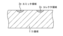
本実施形態では、図1Aに示すように、B(ホウ素)イオンがドーピングされたp型のSi基板1の表面の2箇所にn型のエミッタ領域2e及びコレクタ領域2cを形成する。例えば、Si基板1の厚さは625±15μm程度であり、その比抵抗は10〜20(Ω・cm)であり、その表面は(1−1−1)面となっている。エミッタ領域2e及びコレクタ領域2cの形成に当たっては、二次イオン質量分析器(IMA(Ion Micro Analyzer))により加速電圧を20kV、イオン電流を10μAとして、希ガス元素のイオンであるAr+及びHe+を2時間程度、Si基板1の2箇所にイオン照射する。この結果、Si基板1の格子原子が蹴り出され、空格子が生じ、Si基板1の表面から比較的深い位置までダングリングボンドが生成される。これらのダングリングボンドが生成された領域がn型のエミッタ領域2e及びコレクタ領域2cとなる。なお、エミッタ領域2e及びコレクタ領域2cの間隔は、例えば1.5mm程度とし、エミッタ領域2e及びコレクタ領域2cの直径は、例えば0.5mm程度とする。
In this embodiment, as shown in FIG. 1A, an n-
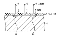
次に、図1Bに示すように、Si基板1上に厚さが20μm〜30μm程度のマイカ箔3を形成する。次いで、マイカ箔3のエミッタ領域2e及びコレクタ領域2cに整合する2箇所の領域並びにこれらの中心近傍の領域にコンタクトホールを形成する。その後、これらのコンタクトホール内に炭素電極塗料を用いて電極4を埋め込む。なお、各コンタクトホールの直径は、例えば0.3mmとする。続いて、電極4毎にCu配線5を形成する。
Next, as shown in FIG. 1B, a mica foil 3 having a thickness of about 20 μm to 30 μm is formed on the
このようにして形成された半導体装置においては、図1に示すように、エミッタ領域2eとコレクタ領域2cとの間にp型の領域が存在し、このp型の領域がベースとして作用する。つまり、バイポーラトランジスタが形成されている。そして、このバイポーラトランジスタは、ダングリングボンドを用いて構成されているため、従来のn型不純物及びp型不純物を用いて構成されたバイポーラトランジスタと比較して、熱的安定性に優れている。即ち、従来のバイポーラトランジスタでは、高温になるとドーピングされているイオンの拡散に伴って動作が不安定となるが、本実施形態に係るバイポーラトランジスタでは、そのような拡散が生じない。また、イオンの拡散が生じないため、集積性を向上させることも可能である。
In the semiconductor device formed in this way, as shown in FIG. 1, a p-type region exists between the
なお、上述のような効果はバイポーラトランジスタだけでなくダイオードにおいても同様に得られる。 The effect as described above can be obtained not only in the bipolar transistor but also in the diode.
次に、本願発明者が実際に行った実験の結果について説明する。 Next, the results of experiments actually performed by the present inventors will be described.
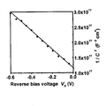
先ず、上述の実施形態と同様にして、n型の領域を1箇所のみに形成することにより、ダイオードを作製し、基板のドナー濃度及び拡散電位を求めた。ここでは、先ず、逆バイアス電圧VR(V)と空乏層容量C(F/cm2)との関係を求めた。一般に、逆バイアス電圧VRと空乏層容量Cとの関係は、下記数1で表される。ここで、qは電子1個当たりの電荷(C)、εsは半導体の誘電率(F/cm)、NBはドナー濃度(cm-3)、Vbiは拡散電位(V)である。
First, in the same manner as in the above-described embodiment, an n-type region was formed in only one place to produce a diode, and the donor concentration and diffusion potential of the substrate were obtained. Here, first, the relationship between the reverse bias voltage V R (V) and the depletion layer capacitance C (F / cm 2 ) was obtained. In general, the relationship between the reverse bias voltage V R and the depletion layer capacitance C is expressed by the following
数1から明らかなように、1/C2はVRの1次関数で表され、その傾きからドナー濃度NBが求められ、1/C2が0となるときの切片(VRの値)から拡散電位Vbiを求めることができる。実際に測定して得られた結果を図2に示す。図2より、ドナー濃度NBは3.9×1013(cm-3)であり、拡散電位Vbiは0.35(V)であった。このドナー濃度NBの値は、一般に多用されているn型不純物領域とp型不純物領域とからなるダイオードのドナー濃度の10-3〜10-4程度と低い。
As is evident from the
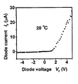
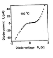
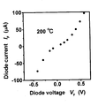
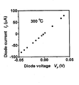
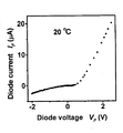
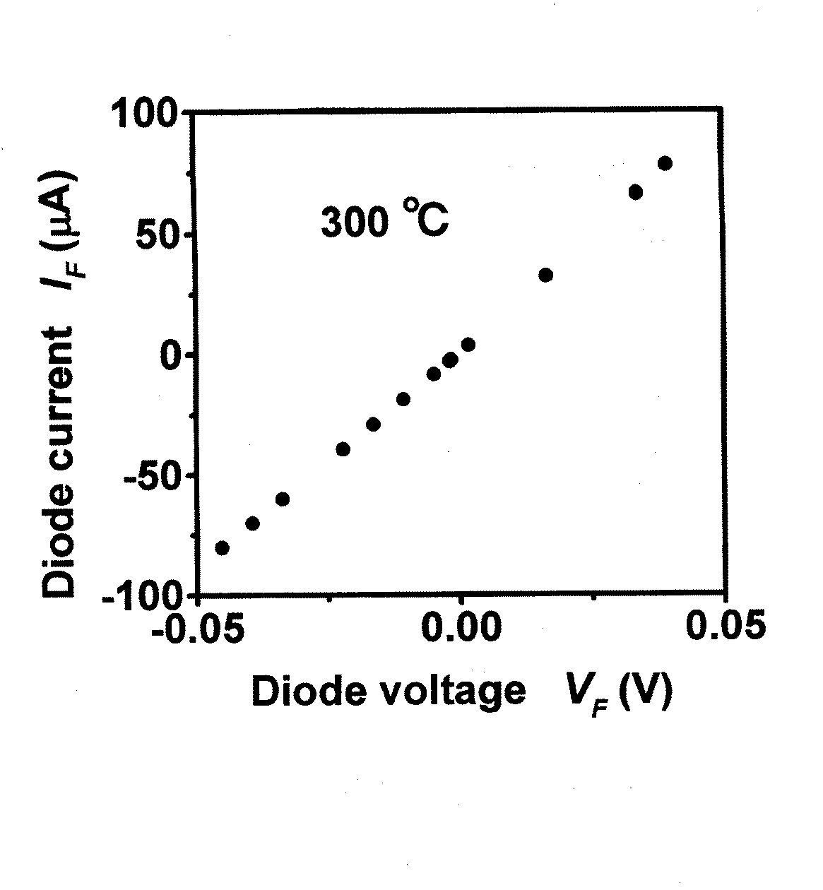
本願発明者は、ダイオードの耐熱性を評価するために、20℃〜300℃の間でダイオード特性の測定を行った。20℃、100℃、200℃、300℃で測定した結果を、夫々図3、図4、図5、図6に示す。図3〜図5から、温度が上昇するに連れてダイオード特性が消失していく過程を読み取ることができる。このような傾向は、熱励起によるキャリアの影響による。また、図6では、ほとんどダイオード特性が残っていない。更に、本願発明者が300℃まで加熱した後に20℃まで温度を下げたダイオードについてその特性を測定したところ、図7に示すような結果が得られた。つまり、300℃まで昇温すると、一旦ダイオード特性が消失するが、その後に降温することにより、再度ダイオード特性が発現するようになる。 The inventor of the present application measured diode characteristics between 20 ° C. and 300 ° C. in order to evaluate the heat resistance of the diode. The results measured at 20 ° C., 100 ° C., 200 ° C., and 300 ° C. are shown in FIGS. 3, 4, 5, and 6, respectively. From FIG. 3 to FIG. 5, it is possible to read the process in which the diode characteristics disappear as the temperature rises. Such a tendency is due to the influence of carriers due to thermal excitation. In FIG. 6, almost no diode characteristics remain. Furthermore, when the inventors measured the characteristics of the diode heated to 300 ° C. and then lowered to 20 ° C., the results shown in FIG. 7 were obtained. That is, once the temperature is raised to 300 ° C., the diode characteristics once disappear, but when the temperature is lowered after that, the diode characteristics again appear.
次に、上述の実施形態と同様にして作製したダイオードの温度特性を測定した結果を図8に示す。温度により、3つの段階(StageI、StageII、StageIII)が出現した。StageI(約100℃以上)では、活性化エネルギーが1.1eVであった。この値は、Siのギャップエネルギー(1.17eV)とほぼ一致しており、StageIは真性領域となっていることを示唆している。このような比較的低い温度から真性領域の出現は、ホウ素(B)によるアクセプタをダングリングボンドの電子が局所的に補償しているため、結晶の純度が上がったように見える。なお、高温下では、電気伝導度に大きな影響を与える主なキャリアは、熱励起でギャップエネルギーを超えるようになった電子となり、ダイオード特性が消失し始める。 Next, FIG. 8 shows the results of measuring the temperature characteristics of a diode manufactured in the same manner as in the above embodiment. Depending on the temperature, three stages (Stage I, Stage II, Stage III) appeared. In Stage I (about 100 ° C. or higher), the activation energy was 1.1 eV. This value almost coincides with the gap energy of Si (1.17 eV), suggesting that Stage I is an intrinsic region. The appearance of the intrinsic region from such a relatively low temperature seems to increase the purity of the crystal because the dangling bond electrons locally compensate the boron (B) acceptor. Note that at high temperatures, the main carriers that have a large effect on electrical conductivity are electrons that have exceeded the gap energy by thermal excitation, and diode characteristics begin to disappear.
なお、ダングリングボンドにより生じたキャリアと同数のキャリアが生成される温度がダイオード特性の熱限界となる。そして、上述のドナー濃度NBが3.9×10¹³(cm-3)のダイオードでは、図4に示すように、100℃でも十分なダイオード特性が得られている。このとき、図8より、導電率σの自然対数は−10程度である。従って、このダイオードのドナー濃度を104倍程度とすると、導電率σの自然対数は−6程度となり、このときの温度は、図8より300℃程度となる。なお、上述のダイオードのドナー濃度を104倍程度とした場合には、一般に多用されているn型不純物領域とp型不純物領域とからなるダイオードのドナー濃度と同程度となる。また、SiCのギャップエネルギーはSiのそれの約2.6倍であるため、半導体基板をSiCから構成した場合には、耐熱温度が900℃程度のトランジスタが得られると考えられる。 Note that the temperature at which the same number of carriers as those generated by dangling bonds is generated is the thermal limit of the diode characteristics. Then, in the diode of the above donor concentration N B is 3.9 × 10 13 (cm -3) , as shown in FIG. 4, a sufficient diode characteristic even 100 ° C. are obtained. At this time, from FIG. 8, the natural logarithm of the conductivity σ is about −10. Therefore, when the donor concentration of this diode is about 10 4 times, the natural logarithm of the conductivity σ is about −6, and the temperature at this time is about 300 ° C. from FIG. When the donor concentration of the above-mentioned diode is about 10 4 times, the donor concentration of the diode composed of the n-type impurity region and the p-type impurity region, which are commonly used, is almost the same. Since the gap energy of SiC is about 2.6 times that of Si, it is considered that a transistor having a heat resistant temperature of about 900 ° C. can be obtained when the semiconductor substrate is made of SiC.
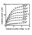
また、本願発明者は、上述の実施形態のようにして作製したバイポーラトランジスタについて、ベース電流IBを変化させながら、コレクタ−エミッタ間電圧VCEとコレクタ電流ICとの関係を求めた。この結果を図9に示す。また、図10には、コレクタ−エミッタ間電圧が5Vのときのベース電流IBとコレクタ電流ICとの関係を示す。図10より、電流増幅率hfe(=IC/IE)は1.1であった。 Further, the inventor of the present application obtained the relationship between the collector-emitter voltage V CE and the collector current I C while changing the base current I B for the bipolar transistor manufactured as in the above-described embodiment. The result is shown in FIG. FIG. 10 shows the relationship between the base current I B and the collector current I C when the collector-emitter voltage is 5V. From FIG. 10, the current amplification factor h fe (= I C / I E ) was 1.1.
更に、本願発明者は、p型炭化珪素基板にヘリウムイオンを加速電圧20kVで打ち込むことにより、この打ち込み場所にダングリングボンドを発生させ、この場所の導電型をn型とした。このようにして作成したpnダイオードの耐熱特性を図11に示す。図11に示すように、400℃以下においてダイオード特性が発現した。 Furthermore, the inventor of the present application implants helium ions into a p-type silicon carbide substrate at an acceleration voltage of 20 kV, thereby generating a dangling bond at this implantation location, and setting the conductivity type at this location to n-type. FIG. 11 shows the heat resistance characteristics of the pn diode thus prepared. As shown in FIG. 11, diode characteristics were developed at 400 ° C. or lower.
なお、ダングリングボンドの発生に当たっては、Ar及びHe等の希ガス元素のイオンの他、D(重水素)イオン又はHイオンをp型の半導体領域に打ち込んでもよい。但し、打ち込んだイオンとダングリングボンドとの結合を防止するためには、希ガス元素のイオンを打ち込むことが好ましい。 In generating a dangling bond, in addition to ions of rare gas elements such as Ar and He, D (deuterium) ions or H ions may be implanted into the p-type semiconductor region. However, it is preferable to implant ions of a rare gas element in order to prevent bonding between the implanted ions and dangling bonds.
1:Si基板
2e:エミッタ領域
2c:コレクタ領域
3:マイカ箔
4:電極
5:Cu配線
1:
Claims (7)
前記第1の半導体領域と隣接し、ダングリングボンドを電子の供給源とするn型の第2の半導体領域と、
を有し、
前記第1の半導体領域及び前記第2の半導体領域はシリコン又は炭化珪素からなることを特徴とする半導体装置。 a p-type first semiconductor region;
An n-type second semiconductor region adjacent to the first semiconductor region and having a dangling bond as an electron source;
Have
The semiconductor device, wherein the first semiconductor region and the second semiconductor region are made of silicon or silicon carbide.
前記第1の半導体領域及び前記第2の半導体領域はシリコン又は炭化珪素からなることを特徴とする半導体装置の製造方法。 forming a dangling bond in the p-type first semiconductor region to form an n-type second semiconductor region using the dangling bond as an electron supply source ;
The method for manufacturing a semiconductor device, wherein the first semiconductor region and the second semiconductor region are made of silicon or silicon carbide.
Priority Applications (1)
| Application Number | Priority Date | Filing Date | Title |
|---|---|---|---|
| JP2006044370A JP5167478B2 (en) | 2005-02-22 | 2006-02-21 | Semiconductor device and manufacturing method thereof |
Applications Claiming Priority (3)
| Application Number | Priority Date | Filing Date | Title |
|---|---|---|---|
| JP2005046087 | 2005-02-22 | ||
| JP2005046087 | 2005-02-22 | ||
| JP2006044370A JP5167478B2 (en) | 2005-02-22 | 2006-02-21 | Semiconductor device and manufacturing method thereof |
Publications (2)
| Publication Number | Publication Date |
|---|---|
| JP2006270074A JP2006270074A (en) | 2006-10-05 |
| JP5167478B2 true JP5167478B2 (en) | 2013-03-21 |
Family
ID=37205632
Family Applications (1)
| Application Number | Title | Priority Date | Filing Date |
|---|---|---|---|
| JP2006044370A Active JP5167478B2 (en) | 2005-02-22 | 2006-02-21 | Semiconductor device and manufacturing method thereof |
Country Status (1)
| Country | Link |
|---|---|
| JP (1) | JP5167478B2 (en) |
Family Cites Families (3)
| Publication number | Priority date | Publication date | Assignee | Title |
|---|---|---|---|---|
| JPH02217397A (en) * | 1989-02-15 | 1990-08-30 | Kobe Steel Ltd | Vapor-phase synthesis of thin film of n-type semiconductor diamond |
| JPH09129902A (en) * | 1995-11-01 | 1997-05-16 | Fujitsu Ltd | Semiconductor device and manufacturing method thereof |
| JPH09320972A (en) * | 1996-05-28 | 1997-12-12 | Kobe Steel Ltd | Method for introducing impurities into semiconductor substrate and method for manufacturing semiconductor device |
-
2006
- 2006-02-21 JP JP2006044370A patent/JP5167478B2/en active Active
Also Published As
| Publication number | Publication date |
|---|---|
| JP2006270074A (en) | 2006-10-05 |
Similar Documents
| Publication | Publication Date | Title |
|---|---|---|
| Graul et al. | High-performance transistors with arsenic-implanted polysil emitters | |
| JPH0845869A (en) | Treatment for localized shortening of charge carrier lifetime, especially in integrated electronic device, and integrated electronic device with localized shortening of charge carrier lifetime | |
| JP3727827B2 (en) | Semiconductor device | |
| WO2021075330A1 (en) | Semiconductor device and method for manufacturing semiconductor device | |
| Tang et al. | An implanted-emitter 4H-SiC bipolar transistor with high current gain | |
| US5756387A (en) | Method for forming zener diode with high time stability and low noise | |
| JPS6112388B2 (en) | ||
| CN108155225A (en) | Constant current device and its manufacturing method | |
| TWI474481B (en) | High gain constant β bipolar junction transistor and manufacturing method thereof | |
| CN101536177B (en) | Semiconductor wafer suitable for forming semiconductor junction diode device and method for forming same | |
| US6770912B2 (en) | Semiconductor device and method for producing the same | |
| JP5167478B2 (en) | Semiconductor device and manufacturing method thereof | |
| CN107534059B (en) | Semiconductor device and manufacturing method of semiconductor device | |
| JP2009004763A (en) | Semiconductor device | |
| JP2022124784A (en) | Semiconductor device and method of manufacturing the same | |
| CN110164814B (en) | SOI substrate and method for producing the same | |
| JP2008535214A (en) | Diode structure | |
| JP4857590B2 (en) | Semiconductor element | |
| CN114051653A (en) | Semiconductor device and method for manufacturing semiconductor device | |
| EP0109888A2 (en) | Subsurface Zener diode | |
| CN114695513B (en) | Semiconductor devices and manufacturing methods thereof | |
| JP2817247B2 (en) | Semiconductor device | |
| JP2841419B2 (en) | Polycrystalline diode and method of manufacturing the same | |
| JPH0233976A (en) | zener diode | |
| JP7415913B2 (en) | Semiconductor device and its manufacturing method |
Legal Events
| Date | Code | Title | Description |
|---|---|---|---|
| A621 | Written request for application examination |
Free format text: JAPANESE INTERMEDIATE CODE: A621 Effective date: 20080709 |
|
| A977 | Report on retrieval |
Free format text: JAPANESE INTERMEDIATE CODE: A971007 Effective date: 20120316 |
|
| A131 | Notification of reasons for refusal |
Free format text: JAPANESE INTERMEDIATE CODE: A131 Effective date: 20120327 |
|
| A521 | Request for written amendment filed |
Free format text: JAPANESE INTERMEDIATE CODE: A523 Effective date: 20120522 |
|
| A131 | Notification of reasons for refusal |
Free format text: JAPANESE INTERMEDIATE CODE: A131 Effective date: 20120731 |
|
| A521 | Request for written amendment filed |
Free format text: JAPANESE INTERMEDIATE CODE: A523 Effective date: 20120924 |
|
| A01 | Written decision to grant a patent or to grant a registration (utility model) |
Free format text: JAPANESE INTERMEDIATE CODE: A01 Effective date: 20121127 |