JP5164635B2 - Signal processing apparatus, droplet discharge apparatus, and signal processing method - Google Patents
Signal processing apparatus, droplet discharge apparatus, and signal processing method Download PDFInfo
- Publication number
- JP5164635B2 JP5164635B2 JP2008086939A JP2008086939A JP5164635B2 JP 5164635 B2 JP5164635 B2 JP 5164635B2 JP 2008086939 A JP2008086939 A JP 2008086939A JP 2008086939 A JP2008086939 A JP 2008086939A JP 5164635 B2 JP5164635 B2 JP 5164635B2
- Authority
- JP
- Japan
- Prior art keywords
- substrate
- analog
- digital
- signal
- analog signal
- Prior art date
- Legal status (The legal status is an assumption and is not a legal conclusion. Google has not performed a legal analysis and makes no representation as to the accuracy of the status listed.)
- Expired - Fee Related
Links
Images


Classifications
-
- B—PERFORMING OPERATIONS; TRANSPORTING
- B41—PRINTING; LINING MACHINES; TYPEWRITERS; STAMPS
- B41J—TYPEWRITERS; SELECTIVE PRINTING MECHANISMS, i.e. MECHANISMS PRINTING OTHERWISE THAN FROM A FORME; CORRECTION OF TYPOGRAPHICAL ERRORS
- B41J2/00—Typewriters or selective printing mechanisms characterised by the printing or marking process for which they are designed
- B41J2/005—Typewriters or selective printing mechanisms characterised by the printing or marking process for which they are designed characterised by bringing liquid or particles selectively into contact with a printing material
- B41J2/01—Ink jet
- B41J2/015—Ink jet characterised by the jet generation process
- B41J2/04—Ink jet characterised by the jet generation process generating single droplets or particles on demand
- B41J2/045—Ink jet characterised by the jet generation process generating single droplets or particles on demand by pressure, e.g. electromechanical transducers
- B41J2/04501—Control methods or devices therefor, e.g. driver circuits, control circuits
- B41J2/04581—Control methods or devices therefor, e.g. driver circuits, control circuits controlling heads based on piezoelectric elements
-
- B—PERFORMING OPERATIONS; TRANSPORTING
- B41—PRINTING; LINING MACHINES; TYPEWRITERS; STAMPS
- B41J—TYPEWRITERS; SELECTIVE PRINTING MECHANISMS, i.e. MECHANISMS PRINTING OTHERWISE THAN FROM A FORME; CORRECTION OF TYPOGRAPHICAL ERRORS
- B41J2/00—Typewriters or selective printing mechanisms characterised by the printing or marking process for which they are designed
- B41J2/005—Typewriters or selective printing mechanisms characterised by the printing or marking process for which they are designed characterised by bringing liquid or particles selectively into contact with a printing material
- B41J2/01—Ink jet
- B41J2/015—Ink jet characterised by the jet generation process
- B41J2/04—Ink jet characterised by the jet generation process generating single droplets or particles on demand
- B41J2/045—Ink jet characterised by the jet generation process generating single droplets or particles on demand by pressure, e.g. electromechanical transducers
- B41J2/04501—Control methods or devices therefor, e.g. driver circuits, control circuits
- B41J2/04541—Specific driving circuit
Landscapes
- Particle Formation And Scattering Control In Inkjet Printers (AREA)
- Ink Jet (AREA)
Description
本発明は、信号処理装置、液滴吐出装置及び信号処理方法に関する。 The present invention relates to a signal processing device, a droplet discharge device, and a signal processing method.
圧電素子に電圧を印加し、当該圧電素子を変形させることにより液滴を吐出する液滴吐出装置が知られている(例えば、特許文献1参照。)。 There is known a droplet discharge device that discharges droplets by applying a voltage to a piezoelectric element and deforming the piezoelectric element (see, for example, Patent Document 1).
図12は、液滴吐出装置における圧電素子に電圧を印加する従来の駆動回路の構成例を示す回路図である。 FIG. 12 is a circuit diagram showing a configuration example of a conventional drive circuit that applies a voltage to a piezoelectric element in a droplet discharge device.
同図に示されるように、この駆動回路300は、デジタル・アナログ・コンバータ302、オペアンプ304及び電流増幅回路306を含んで構成されている。デジタル・アナログ・コンバータ302、オペアンプ304及び電流増幅回路306は直列に接続されている。また、電流増幅回路306には、スイッチング素子308を介して圧電素子310が接続されている。
As shown in the figure, the
ここで、デジタル・アナログ・コンバータ302に対して圧電素子310に印加する電圧の基準となる電圧を示すデジタル信号が入力されると、デジタル・アナログ・コンバータ302では、当該デジタル信号がアナログ信号に変換される。そして、当該アナログ信号はオペアンプ304で電圧増幅され、電流増幅回路306で電流増幅されてスイッチング素子308に出力される。
Here, when a digital signal indicating a voltage that is a reference voltage applied to the
スイッチング素子308は、図示しないコントロール信号によって導通状態と切断状態との2つの状態の間で切り替えられ、スイッチング素子308が導通状態のときに圧電素子310に電流増幅回路306から出力されたアナログ信号の電圧が印加される。
The
ところで、以上のような駆動回路は一般に1枚の基板上に構成されているため、当該駆動回路を構成している部品の一部が故障した場合でも、駆動回路全体を交換することになる。この場合、故障していない部品も交換することになってしまうため、コスト的な無駄が生じる。 By the way, since the drive circuit as described above is generally formed on a single substrate, even if a part of the components constituting the drive circuit fails, the entire drive circuit is replaced. In this case, parts that have not failed are also replaced, resulting in cost waste.
そこで、このような事態を回避する方法として、駆動回路を分割して複数の基板を構成し、故障している部品が含まれる基板のみ交換する方法が考えられる。この場合、駆動回路を分割する位置としては、オペアンプと電流増幅回路との間と、デジタル・アナログ・コンバータとオペアンプとの間とが考えられるが、前者の位置は、後者の位置と比較して、NPN,PNPトランジスタに電流を流すために接続する線を太く且つ短くする必要があり、且つ、負帰還ループもノイズ混入を避ける意味で短くする必要があることを考慮すると後者の位置の方が好ましい。 Therefore, as a method for avoiding such a situation, a method is conceivable in which a drive circuit is divided to form a plurality of boards, and only a board including a failed component is replaced. In this case, the drive circuit can be divided between the operational amplifier and the current amplifier circuit, and between the digital-analog converter and the operational amplifier. The former position is compared with the latter position. In consideration of the fact that it is necessary to make the connecting line thick and short in order to pass the current to the NPN and PNP transistors, and that the negative feedback loop needs to be shortened in order to avoid noise contamination, the latter position is more suitable. preferable.
ところで、上述したような駆動回路が構成された基板をデジタル・アナログ・コンバータとオペアンプとの間で分割して得られた各基板をコネクタを介して接続した場合、基板間の接続状態が良好であれば、スイッチング素子のドレイン−ソース間を導通状態にすることにより当該スイッチング素子を介して圧電素子に駆動用の電圧が印加される。なお、従来の駆動回路では、スイッチング素子のドレイン−ソース間に電位差が生じないように制御が行われる。
しかしながら、コネクタの接続不良が生じた場合、スイッチング素子に圧電素子を駆動させるための電圧が印加されると、コネクタ接続の前後でスイッチング素子の両端において過大な電位差が生じてスイッチング素子が破損してしまう虞がある、という問題点があった。なお、この問題点は圧電素子に限らず、他の容量性負荷においても生じ得る問題点である。 However, when a connector connection failure occurs, if a voltage for driving the piezoelectric element is applied to the switching element, an excessive potential difference occurs at both ends of the switching element before and after the connector connection, and the switching element is damaged. There was a problem that there was a risk of it. This problem is not limited to the piezoelectric element, and may occur even in other capacitive loads.
本発明は上記問題点を解決するために成されたものであり、コネクタの接続不良に起因するスイッチング素子の破損を防止することができる信号処理装置、液滴吐出装置及び信号処理方法を提供することを目的とする。 The present invention has been made to solve the above problems, and provides a signal processing device, a droplet discharge device, and a signal processing method capable of preventing the switching element from being damaged due to poor connection of a connector. For the purpose.
上記目的を達成するために、請求項1に記載の信号処理装置は、容量性負荷に印加する電圧の基準となるデジタル信号をアナログ信号に変換して該アナログ信号を差動出力するデジタル・アナログ・コンバータを有する第1の基板と、スイッチング素子を介して前記容量性負荷に接続された出力端を有するオペアンプであって、前記デジタル・アナログ・コンバータから差動出力された前記アナログ信号が入力され、入力された前記アナログ信号の電圧を増幅して出力するオペアンプを有する第2の基板と、前記デジタル・アナログ・コンバータから出力された前記アナログ信号が前記オペアンプの入力端に入力されるように前記第1の基板と前記第2の基板とを機械的に接続するコネクタと、前記第1の基板に設けられ、所定信号を前記第2の基板に前記コネクタを介して送信する送信手段と、電力供給源から駆動用電力が供給されることによって駆動する差動増幅回路であって、前記第2の基板において前記オペアンプの前段に設けられると共に、前記デジタル・アナログ・コンバータから差動出力された前記アナログ信号が入力され、当該アナログ信号を差動増幅する差動増幅回路と、前記第2の基板に設けられた制御手段であって、前記第2の基板において前記所定信号が受信されていない場合、前記差動増幅回路に前記駆動用電力が供給されないように前記差動増幅回路を制御する制御手段と、を備えている。 In order to achieve the above object, the signal processing apparatus according to claim 1 is a digital / analog which converts a digital signal which is a reference of a voltage applied to a capacitive load into an analog signal and differentially outputs the analog signal. An operational amplifier having a first substrate having a converter and an output terminal connected to the capacitive load via a switching element, to which the analog signal differentially output from the digital-analog converter is input; A second substrate having an operational amplifier that amplifies and outputs the voltage of the input analog signal, and the analog signal output from the digital-analog converter is input to an input terminal of the operational amplifier. A connector that mechanically connects the first substrate and the second substrate; and a first signal provided on the first substrate, the predetermined signal being transmitted to the first substrate. Transmitting means for transmitting to the substrate via the connector, and a differential amplifier circuit driven by driving power supplied from a power supply source, provided on the second substrate in front of the operational amplifier And a differential amplifier circuit for differentially amplifying the analog signal to which the analog signal differentially output from the digital-analog converter is input, and a control means provided on the second substrate, Control means for controlling the differential amplifier circuit so that the driving power is not supplied to the differential amplifier circuit when the predetermined signal is not received by the second substrate.
このように、本発明によれば、コネクタを介して受信されるべき所定信号が受信されていない場合、当該コネクタに接続不良が生じているものとみなして、スイッチング素子を介して容量性負荷にアナログ信号の電圧が印加されないように制御を行うので、コネクタの接続不良に起因するスイッチング素子の破損を防止することができる。 Thus, according to the present invention, when a predetermined signal to be received via a connector is not received, it is assumed that a connection failure has occurred in the connector, and a capacitive load is applied via the switching element. Since control is performed so that the voltage of the analog signal is not applied, it is possible to prevent the switching element from being damaged due to poor connection of the connector.
また、第2の基板において、コネクタの部分でアナログ信号に重畳されたノイズを小さくすることができる。 Further, in the second board, noise superimposed on the analog signal at the connector portion can be reduced.
また、低コストで、かつ確実にコネクタの接続不良に起因するスイッチング素子の破損を防止することができる。 Further , it is possible to reliably prevent the switching element from being damaged due to poor connection of the connector at low cost.
上記目的を達成するために、請求項2に記載の信号処理装置は、容量性負荷に印加する電圧の基準となるデジタル信号をアナログ信号に変換して該アナログ信号を差動出力するデジタル・アナログ・コンバータを有する第1の基板と、スイッチング素子を介して前記容量性負荷に接続された出力端を有するオペアンプであって、前記デジタル・アナログ・コンバータから差動出力された前記アナログ信号が入力され、入力された前記アナログ信号の電圧を増幅して出力するオペアンプを有する第2の基板と、前記デジタル・アナログ・コンバータから出力された前記アナログ信号が前記オペアンプの入力端に入力されるように前記第1の基板と前記第2の基板とを機械的に接続するコネクタと、前記第1の基板に設けられ、所定信号を前記第2の基板に前記コネクタを介して送信する送信手段と、前記第2の基板において前記オペアンプの前段に設けられると共に、前記デジタル・アナログ・コンバータから差動出力された前記アナログ信号が入力され、当該アナログ信号を差動増幅する差動増幅回路と、前記差動増幅回路と前記オペアンプとを電気的に接続可能なスイッチと、前記第2の基板に設けられた制御手段であって、前記第2の基板において前記所定信号が受信されていない場合、前記差動増幅回路と前記オペアンプとを電気的に切断するように前記スイッチをスイッチング制御する制御手段と、を備えている。
上記目的を達成するために、請求項3に記載の信号処理装置は、容量性負荷に印加する電圧の基準となるデジタル信号をアナログ信号に変換して該アナログ信号を差動出力するデジタル・アナログ・コンバータを有する第1の基板と、スイッチング素子を介して前記容量性負荷に接続された出力端を有するオペアンプであって、前記デジタル・アナログ・コンバータから差動出力された前記アナログ信号が入力され、入力された前記アナログ信号の電圧を増幅して出力するオペアンプを有する第2の基板と、前記デジタル・アナログ・コンバータから出力された前記アナログ信号が前記オペアンプの入力端に入力されるように前記第1の基板と前記第2の基板とを機械的に接続するコネクタと、前記第1の基板に設けられ、所定信号を前記第2の基板に前記コネクタを介して送信する送信手段と、前記スイッチング素子と前記出力端との間に挿入されると共に前記オペアンプと前記スイッチング素子とを電気的に接続可能なスイッチと、前記第2の基板に設けられた制御手段であって、前記第2の基板において前記所定信号が受信されていない場合、前記オペアンプと前記スイッチング素子とを電気的に切断するように前記スイッチをスイッチング制御する制御手段と、を備えている。
上記目的を達成するために、請求項4に記載の信号処理装置は、複数の容量性負荷の各々に各々対応するように設けられると共に、各々対応する前記容量性負荷に印加する電圧の基準となるデジタル信号をアナログ信号に変換して該アナログ信号を差動出力する複数のデジタル・アナログ・コンバータを有する第1の基板と、前記複数のデジタル・アナログ・コンバータの各々に各々対応するように設けられると共に、各々スイッチング素子を介して対応する前記容量性負荷に接続された出力端を有する複数のオペアンプであって、対応する前記デジタル・アナログ・コンバータから差動出力された前記アナログ信号が入力され、入力された前記アナログ信号の電圧を増幅して出力する複数のオペアンプを有する第2の基板と、前記複数のデジタル・アナログ・コンバータの各々から出力された前記アナログ信号が対応する前記オペアンプの入力端に入力されるように前記第1の基板と前記第2の基板とを機械的に接続する複数のコネクタと、前記第1の基板に設けられ、所定信号を前記第2の基板に前記複数のコネクタを介して送信する送信手段と、電力供給源から駆動用電力が供給されることによって駆動する複数の差動増幅回路であって、前記第2の基板において各々対応する前記オペアンプの前段に設けられると共に、各々対応する前記デジタル・アナログ・コンバータから差動出力された前記アナログ信号が入力され、当該アナログ信号を差動増幅する複数の差動増幅回路と、前記第2の基板に設けられた制御手段であって、前記第2の基板において、前記送信手段により前記複数のコネクタの各々を介して送信された前記所定信号の少なくとも1つが受信されていない場合、該所定信号が介されるべき前記コネクタに対応する前記差動増幅回路に前記駆動用電力が供給されないように前記差動増幅回路を制御する制御手段と、を備えている。これにより、複数の容量性負荷に対応した駆動回路におけるコネクタの接続不良に起因するスイッチング素子の破損を防止することができる。
In order to achieve the above object, the signal processing apparatus according to claim 2 converts a digital signal serving as a reference of a voltage applied to the capacitive load into an analog signal and differentially outputs the analog signal. An operational amplifier having a first substrate having a converter and an output terminal connected to the capacitive load via a switching element, to which the analog signal differentially output from the digital-analog converter is input; A second substrate having an operational amplifier that amplifies and outputs the voltage of the input analog signal, and the analog signal output from the digital-analog converter is input to an input terminal of the operational amplifier. A connector that mechanically connects the first substrate and the second substrate; and a first signal provided on the first substrate, the predetermined signal being transmitted Transmitting means for transmitting to the circuit board via the connector, and the analog signal output differentially from the digital-analog converter is input to the second circuit board in front of the operational amplifier. A differential amplifying circuit for differentially amplifying a signal; a switch capable of electrically connecting the differential amplifying circuit and the operational amplifier; and control means provided on the second substrate, And a control means for switching the switch so as to electrically disconnect the differential amplifier circuit and the operational amplifier when the predetermined signal is not received on the substrate.
In order to achieve the above object, the signal processing apparatus according to
In order to achieve the above object, the signal processing device according to claim 4 is provided so as to correspond to each of the plurality of capacitive loads, and a reference voltage applied to each of the corresponding capacitive loads, A first substrate having a plurality of digital-to-analog converters for converting the digital signal to an analog signal and differentially outputting the analog signal, and corresponding to each of the plurality of digital-to-analog converters A plurality of operational amplifiers each having an output terminal connected to the corresponding capacitive load via a switching element, wherein the analog signal differentially output from the corresponding digital-to-analog converter is input. A second substrate having a plurality of operational amplifiers for amplifying and outputting the voltage of the input analog signal; and A plurality of connectors that mechanically connect the first board and the second board so that the analog signal output from each of the tall analog converters is input to an input terminal of the corresponding operational amplifier; A transmission means provided on the first board for transmitting a predetermined signal to the second board via the plurality of connectors; and a plurality of differences driven by driving power supplied from a power supply source. A dynamic amplification circuit, which is provided in front of each of the corresponding operational amplifiers on the second substrate, and the analog signals differentially output from the corresponding digital-analog converters are input, A plurality of differential amplifying circuits for differentially amplifying the signal and control means provided on the second substrate, wherein the transmitting means is provided on the second substrate. When at least one of the predetermined signals transmitted through each of the plurality of connectors is not received, the driving power is not supplied to the differential amplifier circuit corresponding to the connector through which the predetermined signal is to be transmitted. Control means for controlling the differential amplifier circuit. As a result, it is possible to prevent the switching element from being damaged due to poor connector connection in the drive circuit corresponding to a plurality of capacitive loads.
また、第2の基板において、コネクタの部分でアナログ信号に重畳されたノイズを小さくすることができる。 Further , in the second board, noise superimposed on the analog signal at the connector portion can be reduced.
また、低コストで、かつ確実に、複数の容量性負荷に対応した駆動回路におけるコネクタの接続不良に起因するスイッチング素子の破損を防止することができる。 In addition , the switching element can be prevented from being damaged due to poor connection of the connector in the drive circuit corresponding to a plurality of capacitive loads at a low cost.
上記目的を達成するために、請求項5に記載の信号処理装置は、複数の容量性負荷の各々に各々対応するように設けられると共に、各々対応する前記容量性負荷に印加する電圧の基準となるデジタル信号をアナログ信号に変換して該アナログ信号を差動出力する複数のデジタル・アナログ・コンバータを有する第1の基板と、前記複数のデジタル・アナログ・コンバータの各々に各々対応するように設けられると共に、各々スイッチング素子を介して対応する前記容量性負荷に接続された出力端を有する複数のオペアンプであって、対応する前記デジタル・アナログ・コンバータから差動出力された前記アナログ信号が入力され、入力された前記アナログ信号の電圧を増幅して出力する複数のオペアンプを有する第2の基板と、前記複数のデジタル・アナログ・コンバータの各々から出力された前記アナログ信号が対応する前記オペアンプの入力端に入力されるように前記第1の基板と前記第2の基板とを機械的に接続する複数のコネクタと、前記第1の基板に設けられ、所定信号を前記第2の基板に前記複数のコネクタを介して送信する送信手段と、前記第2の基板において各々対応する前記オペアンプの前段に設けられると共に、各々対応する前記デジタル・アナログ・コンバータから差動出力された前記アナログ信号が入力され、当該アナログ信号を差動増幅する複数の差動増幅回路と、前記複数の差動増幅回路の各々と各々対応する前記オペアンプとを電気的に接続可能な複数のスイッチと、前記第2の基板に設けられた制御手段であって、前記第2の基板において、前記送信手段により前記複数のコネクタの各々を介して送信された前記所定信号の少なくとも1つが受信されていない場合、該所定信号が介されるべき前記コネクタに対応する前記差動増幅回路と該差動増幅回路に対応する前記オペアンプとを電気的に切断するように、対応する前記スイッチをスイッチング制御する制御手段と、を備えている。
上記目的を達成するために、請求項6に記載の信号処理装置は、複数の容量性負荷の各々に各々対応するように設けられると共に、各々対応する前記容量性負荷に印加する電圧の基準となるデジタル信号をアナログ信号に変換して該アナログ信号を差動出力する複数のデジタル・アナログ・コンバータを有する第1の基板と、前記複数のデジタル・アナログ・コンバータの各々に各々対応するように設けられると共に、各々スイッチング素子を介して対応する前記容量性負荷に接続された出力端を有する複数のオペアンプであって、対応する前記デジタル・アナログ・コンバータから差動出力された前記アナログ信号が入力され、入力された前記アナログ信号の電圧を増幅して出力する複数のオペアンプを有する第2の基板と、前記複数のデジタル・アナログ・コンバータの各々から出力された前記アナログ信号が対応する前記オペアンプの入力端に入力されるように前記第1の基板と前記第2の基板とを機械的に接続する複数のコネクタと、前記第1の基板に設けられ、所定信号を前記第2の基板に前記複数のコネクタを介して送信する送信手段と、前記複数のオペアンプの各々について、前記スイッチング素子と前記出力端との間に挿入されると共に前記オペアンプの各々と対応する前記スイッチング素子とを電気的に接続可能な複数のスイッチと、前記第2の基板に設けられた制御手段であって、前記第2の基板において、前記送信手段により前記複数のコネクタの各々を介して送信された前記所定信号の少なくとも1つが受信されていない場合、該所定信号が介されるべき前記コネクタに対応する前記オペアンプと該オペアンプに対応する前記スイッチング素子とを電気的に切断するように、対応する前記スイッチをスイッチング制御する制御手段と、を備えている。
一方、上記目的を達成するために、請求項7に記載の液滴吐出装置は、請求項1〜請求項6の何れか1項に記載の信号処理装置を備え、前記容量性負荷は圧電素子であり、前記圧電素子が駆動されることにより液滴を吐出するノズルを有する液滴吐出ヘッドと、画像情報に基づいて前記ノズルから液滴を記録媒体に吐出させるように前記液滴吐出ヘッドを制御するヘッド制御手段と、を備えている。
In order to achieve the above object, the signal processing device according to claim 5 is provided so as to correspond to each of a plurality of capacitive loads, and a reference of a voltage applied to each of the corresponding capacitive loads, A first substrate having a plurality of digital-to-analog converters for converting the digital signal to an analog signal and differentially outputting the analog signal, and corresponding to each of the plurality of digital-to-analog converters A plurality of operational amplifiers each having an output terminal connected to the corresponding capacitive load via a switching element, wherein the analog signal differentially output from the corresponding digital-to-analog converter is input. A second substrate having a plurality of operational amplifiers for amplifying and outputting the voltage of the input analog signal; and A plurality of connectors that mechanically connect the first board and the second board so that the analog signal output from each of the tall analog converters is input to an input terminal of the corresponding operational amplifier; A transmission means provided on the first substrate, for transmitting a predetermined signal to the second substrate via the plurality of connectors, and provided in front of the corresponding operational amplifier on the second substrate, The analog signals differentially output from the corresponding digital-to-analog converters are input, respectively, and a plurality of differential amplifier circuits for differentially amplifying the analog signals, respectively corresponding to the plurality of differential amplifier circuits A plurality of switches electrically connectable to the operational amplifier, and control means provided on the second substrate, wherein the second substrate includes the switch When at least one of the predetermined signals transmitted via each of the plurality of connectors is not received by a transmission means, the differential amplifier circuit corresponding to the connector through which the predetermined signal is to be transmitted and the differential amplification Control means for switching-controlling the corresponding switch so as to electrically disconnect the operational amplifier corresponding to the circuit.
In order to achieve the above object, the signal processing device according to claim 6 is provided so as to correspond to each of a plurality of capacitive loads, and a reference of a voltage applied to each of the corresponding capacitive loads, A first substrate having a plurality of digital-to-analog converters for converting the digital signal to an analog signal and differentially outputting the analog signal, and corresponding to each of the plurality of digital-to-analog converters A plurality of operational amplifiers each having an output terminal connected to the corresponding capacitive load via a switching element, wherein the analog signal differentially output from the corresponding digital-to-analog converter is input. A second substrate having a plurality of operational amplifiers for amplifying and outputting the voltage of the input analog signal; and A plurality of connectors that mechanically connect the first board and the second board so that the analog signal output from each of the tall analog converters is input to an input terminal of the corresponding operational amplifier; A transmission means provided on the first board for transmitting a predetermined signal to the second board via the plurality of connectors, and between each of the plurality of operational amplifiers, between the switching element and the output terminal. And a plurality of switches electrically connected to the switching elements corresponding to each of the operational amplifiers, and control means provided on the second substrate, wherein the second substrate includes: If at least one of the predetermined signals transmitted via each of the plurality of connectors is not received by the transmitting means, the predetermined signal should be passed And said switching element corresponding to the operational amplifier and the operational amplifier corresponding to the serial connector to electrically disconnect includes a control means for controlling switching of said switch corresponding, the.
On the other hand, in order to achieve the above object, a droplet discharge device according to a seventh aspect includes the signal processing device according to any one of the first to sixth aspects, wherein the capacitive load is a piezoelectric element. A droplet discharge head having a nozzle for discharging a droplet when the piezoelectric element is driven, and the droplet discharge head to discharge a droplet from the nozzle to a recording medium based on image information. Head control means for controlling.
請求項7に記載の液滴吐出装置によれば、圧電素子が駆動されることにより液滴吐出ヘッドのノズルから液滴が吐出される。また、ヘッド制御手段により、画像情報に基づいてノズルから液滴を記録媒体に吐出させるように液滴吐出ヘッドが制御される。 According to the droplet discharge device of the seventh aspect, the droplet is discharged from the nozzle of the droplet discharge head by driving the piezoelectric element. Further, the liquid droplet ejection head is controlled by the head control means so that the liquid droplets are ejected from the nozzles onto the recording medium based on the image information.
従って、本発明の液滴吐出装置によれば、本発明の信号処理装置を有しているので、当該信号処理装置と同様に、コネクタの接続不良に起因するスイッチング素子の破損を防止することができる。 Therefore, according to the droplet discharge device of the present invention, since the signal processing device of the present invention is provided, the switching element can be prevented from being damaged due to poor connection of the connector as in the case of the signal processing device. it can.
一方、上記目的を達成するために、請求項8に記載の信号処理方法は、容量性負荷に印加する電圧の基準となるデジタル信号をアナログ信号に変換して該アナログ信号を差動出力するデジタル・アナログ・コンバータを有する第1の基板とスイッチング素子を介して前記容量性負荷に接続された出力端を有するオペアンプであって、前記デジタル・アナログ・コンバータから差動出力された前記アナログ信号が入力され、入力された前記アナログ信号の電圧を増幅して出力するオペアンプを有する第2の基板とを、前記デジタル・アナログ・コンバータから出力された前記アナログ信号が前記オペアンプの入力端に入力されるように機械的に接続するコネクタを介して、前記第1の基板から所定信号を前記第2の基板にコネクタを介して送信し、電力供給源から駆動用電力が供給されることによって駆動する差動増幅回路であって、前記第2の基板において前記オペアンプの前段に設けられると共に、前記デジタル・アナログ・コンバータから差動出力された前記アナログ信号が入力され、当該アナログ信号を差動増幅する差動増幅回路に対して、前記第2の基板において前記所定信号が受信されていない場合、前記駆動用電力が供給されないように、前記第2の基板に設けられた制御手段により前記差動増幅回路を制御するものとしている。 On the other hand, in order to achieve the above object, the signal processing method according to claim 8 is a digital signal that converts a digital signal that is a reference of a voltage applied to a capacitive load into an analog signal and differentially outputs the analog signal. An operational amplifier having a first substrate having an analog converter and an output terminal connected to the capacitive load via a switching element, wherein the analog signal differentially output from the digital analog converter is input And the second substrate having an operational amplifier that amplifies and outputs the voltage of the input analog signal so that the analog signal output from the digital-analog converter is input to an input terminal of the operational amplifier. A predetermined signal is transmitted from the first board to the second board through the connector mechanically connected to the second board through the connector. A differential amplifier circuit that is driven by power supplied from a power supply source, and is provided in front of the operational amplifier on the second substrate, and is differentially output from the digital-analog converter. When the predetermined signal is not received in the second substrate with respect to the differential amplification circuit that differentially amplifies the analog signal when the analog signal is input, the driving power is not supplied. The differential amplifier circuit is controlled by control means provided on the second substrate.
従って、本発明の信号処理方法によれば、請求項1記載の発明と同様に作用するので、請求項1記載の発明と同様に、コネクタの接続不良に起因するスイッチング素子の破損を防止することができる。 Therefore, according to the signal processing method of the present invention, the operation is the same as that of the first aspect of the invention, so that the switching element is prevented from being damaged due to the poor connection of the connector as in the first aspect of the invention. Can do.
本発明によれば、コネクタの接続不良に起因するスイッチング素子の破損を防止することができる、という効果が得られる。 According to the present invention, it is possible to prevent the switching element from being damaged due to poor connection of the connector.
以下、図面を参照して本発明を実施するための最良の形態について詳細に説明する。なお、以下の実施形態では、本発明に係る液滴吐出装置をインクジェット記録装置に適用した場合について説明する。 The best mode for carrying out the present invention will be described below in detail with reference to the drawings. In the following embodiments, a case where the liquid droplet ejection apparatus according to the present invention is applied to an ink jet recording apparatus will be described.
〔第1の実施形態〕 [First Embodiment]
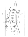
図1は、本第1の実施形態に係るインクジェット記録装置の全体構成を示す構成図である。 FIG. 1 is a configuration diagram showing the overall configuration of the ink jet recording apparatus according to the first embodiment.
同図に示すように、インクジェット記録装置110は、ブラック(K)、シアン(C)、マゼンタ(M)、イエロー(Y)の各インクに対応して設けられた複数のインクジェット記録ヘッド(以下、ヘッドという。)112K,112C,112M,112Yを有する印字部112と、各ヘッド112K,112C,112M,112Yに供給するインクを貯蔵しておくインク貯蔵部114と、記録媒体たる記録紙116を供給する給紙部118と、記録紙116のカールを除去するデカール処理部120と、印字部112のノズル面(インク吐出面)に対向して配置され、記録紙116の平面性を保持しながら記録紙116を搬送するベルト搬送部122と、記録済みの記録紙(プリント物)を外部に排紙する排紙部126と、を備えている。なお、本明細書でいう「印字」とは、文字の印刷の他に画像の印刷も含む。
As shown in the figure, the ink
インク貯蔵部114は、各ヘッド112K,112C,112M,112Yに対応する色のインクを貯蔵するインクタンクを有し、各タンクは所要の管路を介してヘッド112K,112C,112M,112Yと連通されている。また、インク貯蔵部114は、インク残量が少なくなるとその旨を報知する報知手段を備えるとともに、色間の誤装填を防止するための機構を有している。
The
図1では、給紙部118の一例としてロール紙(連続用紙)のマガジンが示されているが、紙幅や紙質等が異なる複数のマガジンを併設しても良い。また、ロール紙のマガジンに代えて、又はこれと併用して、カット紙が積層装填されたカセットによって用紙を供給しても良い。
In FIG. 1, a magazine for rolled paper (continuous paper) is shown as an example of the
複数種類の記録媒体(メディア)を利用可能な構成にした場合、メディアの種類情報を記録したバーコード或いは無線タグなどの情報記録体をマガジンに取り付け、その情報記録体の情報を所定の読取装置によって読み取ることで、使用される記録媒体の種類(メディア種)を自動的に判別し、メディア種に応じて適切なインク吐出を実現するようにインク吐出制御を行うことが好ましい。 When a plurality of types of recording media (media) can be used, an information recording body such as a barcode or a wireless tag that records media type information is attached to a magazine, and information on the information recording body is read by a predetermined reader. It is preferable to automatically determine the type of recording medium to be used (media type) and to perform ink ejection control so as to realize appropriate ink ejection according to the media type.
給紙部118から送り出される記録紙116はマガジンに装填されていたことによる巻きクセが残り、カールする。このカールを除去するために、デカール処理部120においてマガジンの巻きクセ方向と逆方向に加熱ドラム130で記録紙116に圧力を加えながら熱を与える。このとき、多少印字面が外側に弱いカールとなるように加熱温度を制御するとより好ましい。
The
ロール紙を使用する装置構成の場合、図1のように、裁断用のカッター128が設けられており、該カッター128によってロール紙は所望のサイズにカットされる。なお、カット紙を使用する場合には、カッター128は不要である。
In the case of an apparatus configuration using roll paper, a
デカール処理後、カットされた記録紙116は、ベルト搬送部122へと送られる。ベルト搬送部122は、ローラ131,132間に無端状のベルト133が巻き掛けられた構造を有するように構成されている。
After the decurling process, the
ベルト133は、記録紙116の幅よりも広い幅寸法を有しており、ベルト面には多数の吸引穴(不図示)が形成されている。同図に示されるように、ローラ131,132間に掛け渡されたベルト133の内側において印字部112のノズル面には吸着チャンバ134が設けられており、この吸着チャンバ134をファン135で吸引して負圧にすることによって記録紙116がベルト133上に吸着保持される。なお、吸引吸着方式に代えて、静電吸着方式を採用してもよい。
The
ベルト133が巻かれているローラ131,132の少なくとも一方に図示しないモータの動力が伝達されることにより、ベルト133は図1上の時計回り方向に駆動され、ベルト133上に保持された記録紙116は図1の左から右へと搬送される。
The power of a motor (not shown) is transmitted to at least one of the
縁無しプリント等を印字するとベルト133上にもインクが付着するので、ベルト133の外側の所定位置(印字領域以外の適当な位置)にベルト清掃部136が設けられている。ベルト清掃部136の構成について詳細は図示しないが、例えば、ブラシ・ロール、吸水ロール等をニップする方式、清浄エアーを吹き掛けるエアーブロー方式、或いはこれらの組合せなどがある。清掃用ロールをニップする方式の場合、ベルト線速度とローラ線速度を変えると清掃効果が大きい。
Since ink adheres to the
なお、ベルト搬送部122に代えて、ローラ・ニップ搬送機構を用いる態様も考えられるが、印字領域をローラ・ニップ搬送すると、印字直後に用紙の印字面をローラが接触するので画像が滲み易いという問題がある。したがって、本例のように、印字領域では画像面を接触させない吸着ベルト搬送が好ましい。
Although a mode using a roller / nip conveyance mechanism in place of the
ベルト搬送部122により形成される用紙搬送路上において印字部112の上流側には、加熱ファン140が設けられている。加熱ファン140は、印字前の記録紙116に加熱空気を吹き付け、記録紙116を加熱する。印字直前に記録紙116を加熱しておくことにより、インクが着弾後乾き易くなる。
A
印字部112の各ヘッド112K,112C,112M,112Yは、当該インクジェット記録装置110が対象とする記録紙116の最大紙幅に対応する長さを有し、そのノズル面には最大サイズの記録紙116の少なくとも一辺を超える長さ(描画可能範囲の全幅)にわたりインク吐出用のノズルが複数配列されたフルライン型のヘッドとなっている(図2参照)。
Each
ヘッド112K,112C,112M,112Yは、記録紙116の送り方向に沿って上流側からK,C,M,Yの色順に配置され、それぞれのヘッド112K,112C,112M,112Yが記録紙116の搬送方向と略直交する方向に沿って延在するように固定設置される。
The
ベルト搬送部122により記録紙116を搬送しつつ各ヘッド112K,112C,112M,112Yからそれぞれ異色のインクを吐出することにより記録紙116上にカラー画像を形成し得る。
A color image can be formed on the
このように、紙幅の全域をカバーするノズル列を有するフルライン型のヘッド112K,112C,112M,112Yを色別に設ける構成によれば、紙送り方向(副走査方向)について記録紙116と印字部112とを相対的に移動させる動作を1回行うだけで(すなわち1回の副走査で)、記録紙116の全面に画像を記録することができる。これにより、記録ヘッドが紙搬送方向と直交する方向に往復動作するシャトル型ヘッドに比べて高速印字が可能であり、生産性を向上させることができる。
As described above, according to the configuration in which the full-line heads 112K, 112C, 112M, and 112Y having nozzle rows that cover the entire width of the paper are provided for each color, the
なお、本第1の実施形態では、K,C,M,Yの標準色(4色)の構成を例示したが、インク色や色数の組合せについてはこれに限定する必要はなく、必要に応じて淡インク、濃インク、特別色インクを追加しても良い。例えば、ライトシアン、ライトマゼンタなどのライト系インクを吐出するインクジェットヘッドを追加する構成も可能である。また、各色ヘッドの配置順序も特に限定はない。 In the first embodiment, the configuration of the standard colors (4 colors) of K, C, M, and Y is exemplified. However, the combination of the ink color and the number of colors need not be limited to this, and is necessary. Accordingly, light ink, dark ink, and special color ink may be added. For example, it is possible to add an ink jet head that discharges light ink such as light cyan and light magenta. Also, the arrangement order of the color heads is not particularly limited.
ベルト搬送部122により形成される用紙搬送路上において印字部112の下流側には後乾燥部142が設けられている。後乾燥部142は、印字された画像面を乾燥させる手段であり、例えば、加熱ファンが用いられる。印字後のインクが乾燥するまでは印字面と接触することは避けたほうが好ましいので、熱風を吹き付ける方式が好ましい。
A
多孔質のペーパーに染料系インクで印字した場合などでは、加圧によりペーパーの孔を塞ぐことでオゾンなど、染料分子を壊す原因となるものと接触することを防ぐことで画像の耐候性がアップする効果がある。 When printing on porous paper with dye-based ink, the weather resistance of the image is improved by preventing contact with ozone or other things that cause dye molecules to break by pressurizing the paper holes with pressure. There is an effect to.
後乾燥部142の後段には、加熱・加圧部144が設けられている。加熱・加圧部144は、画像表面の光沢度を制御するための手段であり、画像面を加熱しながら所定の表面凹凸形状を有する加圧ローラ145で加圧し、画像面に凹凸形状を転写する。
A heating /
こうして生成されたプリント物は排紙部126から排出される。本来プリントすべき本画像(目的の画像を印刷したもの)とテスト印字とは分けて排出することが好ましい。
The printed matter generated in this manner is outputted from the
なお、本第1の実施形態に係るインクジェット記録装置110では、本画像のプリント物と、テスト印字のプリント物とを選別してそれぞれの排出部126A,126Bへと送るために排紙経路を切り換える不図示の選別手段が設けられている。
In the ink
なお、大きめの用紙に本画像とテスト印字とを同時に並列に形成する場合は、カッター148によってテスト印字の部分を切り離す。また、図には示さないが、本画像の排出部126Aには、オーダー別に画像を集積するソーターが設けられる。
When the main image and the test print are simultaneously formed in parallel on a large sheet, the test print portion is separated by the
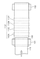
次に、ヘッドの構造について説明する。色別の各ヘッド112K,112C,112M,112Yの構造は共通しているので、以下、これらを代表して符号150によってヘッドを示すものとする。
Next, the structure of the head will be described. Since the structures of the
図3はヘッド150の構造例を示す平面透視図であり、図4はその一部の拡大図である。また、図5は1つの液滴吐出素子(1つのノズル151に対応したインク室ユニット)の立体的構成を示す断面図(図4中の33−33線に沿う断面図)である。
FIG. 3 is a perspective plan view showing a structural example of the
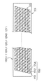
記録紙116上に印字されるドットピッチを高密度化するためには、ヘッド150におけるノズルピッチを高密度化する必要がある。本第1の実施形態に係るヘッド150は、図3及び図4に示されるように、インク吐出口であるノズル151と、各ノズル151に対応する圧力室152等からなる複数のインク室ユニット(液滴吐出素子)153を千鳥でマトリクス状に(2次元的に)配置させた構造を有し、これにより、ヘッド長手方向(紙送り方向と直交する方向)に沿って並ぶように投影される実質的なノズル間隔(投影ノズルピッチ)の高密度化を達成している。
In order to increase the dot pitch printed on the
なお、記録紙116の送り方向と略直交する方向に記録紙116の全幅に対応する長さにわたり1列以上のノズル列を構成する形態は本例に限定されない。
Note that the form in which one or more nozzle rows are formed over a length corresponding to the entire width of the
各ノズル151に対応して設けられている圧力室152は、その平面形状が概略正方形となっており(図3及び図4参照)、対角線上の両隅部の一方にノズル151への流出口が設けられ、他方に供給インクの流入口(供給口)154が設けられている。なお、圧力室152の形状は、本例に限定されず、平面形状が四角形(菱形、長方形など)、五角形、六角形その他の多角形、円形、楕円形など、多様な形態があり得る。
The
図5に示されるように、各圧力室152は供給口154を介して共通流路155と連通されている。共通流路155はインク供給源たるインクタンク(図示省略)と連通しており、インクタンクから供給されるインクは共通流路155を介して各圧力室152に分配供給される。
As shown in FIG. 5, each
圧力室152の一部の面(図5において天面)を構成している加圧板(共通電極と兼用される振動板)156には個別電極157を備えたアクチュエータ158が接合されている。
An
なお、本第1の実施形態に係るアクチュエータ158には、チタン酸ジルコン酸鉛やチタン酸バリウムなどの圧電体を用いた圧電素子が用いられている。
The
アクチュエータ158は、個別電極157と共通電極間に駆動電圧を印加することによって変形して圧力室152の容積が変化し、これに伴う圧力変化によりノズル151からインクが吐出される。本第1の実施形態に係るインク室ユニット153では、インク吐出後、アクチュエータ158の変位が元に戻る際に、共通流路155から供給口154を通って新しいインクが圧力室152に再充填される。
The
従って、本第1の実施形態に係るインクジェット記録装置110では、画像情報から生成されるドット配置データに応じて各ノズル151に対応したアクチュエータ158の駆動を制御することにより、ノズル151からインク滴(液滴)を吐出させることができる。また、本第1の実施形態に係るインクジェット記録装置110では、記録媒体たる記録紙116を一定の速度で副走査方向に搬送しながら、その搬送速度に合わせて各ノズル151のインク吐出タイミングを制御することによって、記録紙116上に所望の画像を記録することができる。
Therefore, in the
上述した構造を有するインク室ユニット153を図6に示す如く主走査方向に沿う行方向及び主走査方向に対して直交しない一定の角度θを有する斜めの列方向に沿って一定の配列パターンで格子状に多数配列させることにより、本第1の実施形態の高密度ノズルヘッドが実現されている。
As shown in FIG. 6, the
すなわち、主走査方向に対してある角度θの方向に沿ってインク室ユニット153を一定のピッチdで複数配列する構造により、主走査方向に並ぶように投影されたノズルのピッチPはd× cosθとなり、主走査方向については、各ノズル151が一定のピッチPで直線状に配列されたものと等価的に取り扱うことができる。このような構成により、主走査方向に並ぶように投影されるノズル列が1インチ当たり2400個(2400ノズル/インチ)におよぶ高密度のノズル構成を実現することが可能になる。
That is, with a structure in which a plurality of
なお、本実施形態では、上述したフルラインヘッドと用紙とを相対移動することによって、上述した主走査で形成された1ライン(1列のドットによるライン又は複数列のドットから成るライン)の印字を繰り返し行うことを副走査と定義する。 In the present embodiment, the above-described full line head and the paper are moved relative to each other to print one line (a line formed by one line of dots or a line composed of a plurality of lines) formed by the main scanning described above. Repeating this is defined as sub-scanning.
また、本実施形態では、上述の主走査によって記録される1ライン(或いは帯状領域の長手方向)の示す方向を主走査方向といい、上述の副走査を行う方向を副走査方向という。すなわち、本実施形態では、記録紙116の搬送方向が副走査方向であり、それに直交する方向が主走査方向ということになる。
In the present embodiment, the direction indicated by one line (or the longitudinal direction of the belt-like region) recorded by the main scanning is referred to as a main scanning direction, and the direction in which the sub scanning is performed is referred to as a sub scanning direction. In other words, in the present embodiment, the conveyance direction of the
図7は、インクジェット記録装置110の電気系の要部構成を示すブロック図である。
FIG. 7 is a block diagram showing the main configuration of the electrical system of the
同図に示されるように、インクジェット記録装置110は、ヘッド150、システム制御部198、プリント制御部180及びヘッドドライバ190を含んで構成される。
As shown in the figure, the ink
システム制御部198は、通信インタフェース170、システムコントローラ172、画像メモリ174、ROM175、モータドライバ176、ヒータドライバ178等を備えている。
The system control unit 198 includes a
通信インタフェース170は、ユーザが当該インクジェット記録装置110に対して印刷の指示等を行うため等に用いられるホスト装置10とのインタフェース部である。通信インタフェース170にはUSB(Universal Serial Bus)、IEEE1394、イーサネット(登録商標)、無線ネットワークなどのシリアルインタフェースやセントロニクスなどのパラレルインタフェースを適用することができる。この部分には、通信を高速化するためのバッファメモリ(図示省略)を搭載しても良い。
The
ホスト装置10から送出された記録紙116に形成すべき画像を示す画像情報は通信インタフェース170を介してインクジェット記録装置110に取り込まれ、一旦画像メモリ174に記憶される。画像メモリ174は、通信インタフェース170を介して入力された画像を記憶する記憶手段であり、システムコントローラ172を通じてデータの読み書きが行われる。画像メモリ174は、半導体素子からなるメモリに限らず、ハードディスクなど磁気媒体を用いてもよい。
Image information indicating an image to be formed on the
システムコントローラ172は、中央演算処理装置(CPU)及びその周辺回路等から構成され、所定のプログラムに従ってインクジェット記録装置110の全体を制御する制御装置として機能するとともに、各種演算を行う演算装置として機能する。すなわち、システムコントローラ172は、通信インタフェース170、画像メモリ174、モータドライバ176、ヒータドライバ178、プリント制御部180等の各部を制御し、ホスト装置10との間の通信制御、画像メモリ174及びROM175の読み書き制御等を行うと共に、搬送系のモータ188やヒータ189を制御する制御信号を生成する。なお、プリント制御部180に対しては、制御信号の他に、画像メモリ174に記憶された画像情報を送信する。
The
また、ROM175には、システムコントローラ172のCPUや後述するヘッドドライバ190のCPU206が実行するプログラム及び制御に必要な各種データなどが格納されている。ROM175は、書換不能な記憶手段であってもよいが、各種のデータを必要に応じて更新する場合は、EEPROMのような書換可能な記憶手段を用いることが好ましい。
The
画像メモリ174は、画像データの一時記憶領域として利用されるとともに、プログラムの展開領域及びCPUの演算作業領域としても利用される。
The
モータドライバ176は、システムコントローラ172からの指示に従って搬送系のモータ188を駆動するドライバ(駆動回路)である。ヒータドライバ178は、システムコントローラ172からの指示に従って後乾燥部142等のヒータ189を駆動するドライバである。
The
プリント制御部180は、システムコントローラ172の制御に従い、システム制御部198から送信された画像情報に基づいてヘッドドライバ190を介してヘッド150を制御する。
The
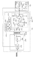
図8は、本第1の実施形態に係るインクジェット記録装置110のヘッド150及びヘッドドライバ190の構成を示す構成図である。
FIG. 8 is a configuration diagram showing the configuration of the
同図に示されるように、ヘッドドライバ190は、第1の基板200及び第2の基板202を含んで構成されている。第1の基板200及び第2の基板202はコネクタ204Aとコネクタ204Bとによりハーネスを介して機械的に接続されている。以下、コネクタ204Aとコネクタ204Bとを区別する必要がない場合には単に「コネクタ204」と称する。
As shown in the figure, the
第1の基板200は、CPU206及びデジタル・アナログ・コンバータ(以下、「D/A変換器」という。)208を含んで構成されている。
The
CPU206は、プリント制御部180に接続されており、プリント制御部180から入力される画像情報に基づいてヘッド150及びヘッドドライバ190の作動を制御する。なお、本第1の実施形態に係るインクジェット記録装置110では、CPU206がプリント制御部180から入力された画像情報に基づいてアクチュエータ158に印加する電圧の基準となる電圧を示すデジタル信号を生成し、当該デジタル信号をD/A変換器208に出力する。
The
D/A変換器208は、CPU206から入力されたデジタル信号をアナログ信号に変換して出力するものである。なお、本第1の実施形態に係るインクジェット記録装置110では、D/A変換器208によって上記アナログ信号が、一例として図9に示すように差動出力される。
The D /
一方、第2の基板202は、差動増幅回路210、アンプ212、CPU214、DC−DCコンバータ216、ROM228及びRAM230を含んで構成されている。
On the other hand, the
差動増幅回路210は、入力端がコネクタ204を介してD/A変換器208の出力端に接続されており、D/A変換器208から差動出力されたアナログ信号が入力され、当該アナログ信号を差動増幅して出力する。
The
アンプ212は、レベルシフト回路218、オペアンプ220及び電流増幅回路222を含んで構成されている。
The
レベルシフト回路218は、オペアンプ223及び直流電源224を含んで構成されている。オペアンプ223は、非反転入力端が差動増幅回路210の出力端に、反転入力端が、マイナス端子が接地された直流電源224のプラス端子に、出力端がオペアンプ220の非反転入力端に各々接続されており、差動増幅回路210から入力されたアナログ信号を電圧レベルを所定の電圧レベル(ヘッド150が良好な液滴吐出を行うことができるものとして予め定められた電圧レベル)だけ嵩上げしてオペアンプ220に出力する。
The
オペアンプ220は、反転入力端が抵抗R1を介して接地されており、出力端が電流増幅回路222の入力端に接続されており、レベルシフト回路218から入力されたアナログ信号を電圧を増幅して電流増幅回路222に出力する。
The
電流増幅回路222は、オペアンプ220から入力されたアナログ信号を電流を増幅してヘッド150に出力するものであり、NPNトランジスタ222aとPNPトランジスタ222bとを含んで構成されている。NPNトランジスタ222aは、ベースがオペアンプ220の出力端に、コレクタが直流電源VHに、エミッタがPNPトランジスタ222bのエミッタに、各々接続されており、PNPトランジスタ222bは、ベースがオペアンプ220の出力端に、コレクタがグランドに各々接続されている。また、NPNトランジスタ222a及びPNPトランジスタ222bの各エミッタは、抵抗R2を介してオペアンプ220の反転入力端に接続されている。
The
DC−DCコンバータ216は、差動増幅回路210に駆動用の電力を供給するものであり、差動増幅回路210は当該電力が供給されることにより作動する。
The DC-
CPU214は、第2の基板202の各部の作動を制御するものである。CPU214は、ROM228及びRAM230の各々に接続されている。また、CPU214は、コネクタ204を介してCPU206に接続されている。更に、CPU214は、DC−DCコンバータ216に接続されている。
The
なお、ROM228には、CPU214が実行するプログラム及び制御に必要な各種データなどが格納されている。また、RAM230は、各種データの一時記憶領域として利用されるとともに、プログラムの展開領域及びCPU214の演算作業領域としても利用される。
The
ヘッド150は、各アクチュエータ158に個別に対応する複数のスイッチ226を含んで構成されている。
The
スイッチ226は、単極単投型スイッチであり、電流増幅回路222の出力端とアクチュエータ158とを接続状態及び非接続状態の2つの状態の間で切り替えるものである。
The
ここで、各スイッチ226はCPU206に接続されている。CPU206は、各スイッチ226を制御するスイッチ制御信号をスイッチ226毎に生成して、対応するスイッチ226に出力する。
Here, each
なお、本第1の実施形態では、スイッチ制御信号がハイ・レベルのとき、対応するスイッチ226がオン状態となり、スイッチ制御信号がロー・レベルのとき、対応するスイッチ226がオフ状態となるが、これに限らず、スイッチ制御信号がロー・レベルのとき、対応するスイッチ226がオン状態となり、スイッチ制御信号がハイ・レベルのとき、対応するスイッチ226がオフ状態となるようにしても良いことは言うまでもない。
In the first embodiment, when the switch control signal is at a high level, the
次に、本第1の実施形態に係るインクジェット記録装置110の作用を説明する。
Next, the operation of the
本第1の実施形態に係るインクジェット記録装置110では、稼動時に、第1の基板200に設けられたCPU206により、所定信号がコネクタ204を介して第2の基板202に出力される。また、プリント制御部180からCPU206に画像情報が入力されると、CPU206により、当該画像情報に基づいてデジタル信号及びスイッチ制御信号が生成され、当該デジタル信号がD/A変換器208に、当該スイッチ制御信号が各スイッチ226に各々出力される。D/A変換器208では、CPU206から入力されたデジタル信号がアナログ信号に変換され、当該アナログ信号がコネクタ204を介して第2の基板202に出力される。
In the
これに対し、第2の基板202に設けられたCPU214では、電圧印加制御処理が実行される。
On the other hand, the voltage application control process is executed in the
以下、図10を参照して、この際の第2の基板202の作用を説明する。なお、図10は、この際にCPU214によって実行される電圧印加制御処理プログラムの処理の流れを示すフローチャートであり、当該プログラムはROM228の所定領域に予め記憶されている。
Hereinafter, the operation of the
同図のステップ300では、CPU206から出力された所定信号を受信したか否かを判定し、肯定判定となった場合にはステップ302へ移行して、スイッチ226を介してアクチュエータ158にアナログ信号の電圧が印加されるように制御(以下、「電圧印加制御」という。)を行い、その後にステップ304へ移行する。
In
本第1の実施形態に係るインクジェット記録装置110では、上記電圧印加制御として、差動増幅回路210を作動させる制御(一例として、DC−DCコンバータ216に対して差動増幅回路210に駆動用の電力を供給させる処理)を適用している。
In the ink
なお、上記電圧印加制御は、これに限らず、例えば、差動増幅回路210とレベルシフト回路218との接続配線を接続と切断の2つの状態間で切り替えるスイッチを設け、差動増幅回路210とレベルシフト回路218とが接続状態となるように当該スイッチを制御する処理を適用しても良い。また、レベルシフト回路218とオペアンプ220との接続配線を接続と切断の2つの状態間で切り替えるスイッチを設け、レベルシフト回路218とオペアンプ220とが接続状態となるように当該スイッチを制御する処理を適用しても良い。また、電流増幅回路222とスイッチ226との接続配線を接続と切断の2つの状態間で切り替えるスイッチを設け、電流増幅回路222とスイッチ226とが接続状態となるように当該スイッチを制御する処理を適用しても良い。
The voltage application control is not limited to this. For example, a switch for switching the connection wiring between the
このように、上記電圧印加制御は、スイッチ226を介してアクチュエータ158にアナログ信号の電圧が印加されるように制御を行う処理であれば如何なるものも適用できる。
As described above, any voltage application control can be applied as long as the control is performed so that the voltage of the analog signal is applied to the
ステップ304では、画像形成(印字)を停止する条件が満足されたか否かを判定し、否定判定となった場合にはステップ300へ戻る一方、肯定判定となった場合には本電圧印加制御処理プログラムを終了する。
In
なお、本第1の実施形態に係るインクジェット記録装置110では、上記画像形成を停止する条件として、インクジェット記録装置110の電源スイッチが切られた、との条件を適用しているが、これに限らず、給紙ユニット34の記録紙116が無くなった、との条件やインクジェット記録装置110において良好な画像形成を行うことができなくなるものとして予め定められた故障が発生した、との条件等を適用しても良い。
In the
一方、ステップ300において否定判定となった場合にはステップ306へ移行し、スイッチ226を介してアクチュエータ158にアナログ信号の電圧が印加されないように制御(以下、「電圧印加禁止制御」という。)を行い、本電圧印加制御処理プログラムを終了する。
On the other hand, if a negative determination is made in
本第1の実施形態に係るインクジェット記録装置110では、上記電圧印加禁止制御として、差動増幅回路210を作動させない制御(一例として、DC−DCコンバータ216に対して差動増幅回路210への駆動用の電力の供給を行わせない処理)を適用している。
In the ink
なお、上記電圧印加禁止制御は、これに限らず、例えば、差動増幅回路210とレベルシフト回路218との接続配線を接続と切断の2つの状態間で切り替えるスイッチを設け、差動増幅回路210とレベルシフト回路218とが非接続状態となるように当該スイッチを制御する処理を適用しても良い。また、レベルシフト回路218とオペアンプ220との接続配線を接続と切断の2つの状態間で切り替えるスイッチを設け、レベルシフト回路218とオペアンプ220とが非接続状態となるように当該スイッチを制御する処理を適用しても良い。更に、電流増幅回路222とスイッチ226との接続配線を接続と切断の2つの状態間で切り替えるスイッチを設け、電流増幅回路222とスイッチ226とが非接続状態となるように当該スイッチを制御する処理を適用しても良い。
The voltage application prohibition control is not limited to this. For example, a switch for switching the connection wiring between the
このように、上記電圧印加禁止制御は、スイッチ226を介してアクチュエータ158にアナログ信号の電圧が印加されないように制御を行う処理であれば如何なるものも適用できる。
As described above, any voltage application prohibition control can be applied as long as it is a process for performing control so that an analog signal voltage is not applied to the
以上詳細に説明したように、本第1の実施形態に係るインクジェット記録装置110によれば、容量性負荷(ここでは、アクチュエータ158)に印加する電圧の基準となるデジタル信号をアナログ信号に変換して出力するD/A変換器208を有する第1の基板200と、出力端がスイッチング素子(ここでは、スイッチ226)を介して容量性負荷に接続され、アナログ信号を電圧を増幅して出力するオペアンプ220を有する第2の基板202と、D/A変換器208から出力されたアナログ信号がオペアンプ220の入力端に入力されるように第1の基板200と第2の基板202とを機械的に接続するコネクタ204と、第1の基板200に設けられ、所定信号を第2の基板202にコネクタ204を介して送信する送信手段(ここでは、CPU206)と、第2の基板202において所定信号が受信されていない場合、スイッチング素子を介して容量性負荷にアナログ信号の電圧が印加されないように制御を行う制御手段(ここでは、CPU214)と、を備えることにより、コネクタ204を介して受信されるべき所定信号が受信されていない場合、当該コネクタ204に接続不良が生じているものとみなして、スイッチング素子を介して容量性負荷にアナログ信号の電圧が印加されないように制御を行うので、コネクタ204の接続不良に起因するスイッチング素子の破損を防止することができる。
As described above in detail, according to the ink
また、本第1の実施形態に係るインクジェット記録装置110によれば、D/A変換器208がアナログ信号を差動出力し、第2の基板202においてオペアンプ220の前段に設けられ、D/A変換器208から差動出力されたアナログ信号が入力され、当該アナログ信号を差動増幅する差動増幅回路210を更に備えたので、第2の基板202において、コネクタ204の部分でアナログ信号に重畳されたノイズを小さくすることができる。
Further, according to the ink
更に、本第1の実施形態に係るインクジェット記録装置110によれば、制御手段が差動増幅回路210を作動させないように制御を行うことにより、容量性負荷にアナログ信号の電圧が印加されないように制御を行うので、低コストで、かつ確実に、コネクタ204の接続不良に起因するスイッチング素子の破損を防止することができる。
Furthermore, according to the ink
〔第2の実施形態〕 [Second Embodiment]
次に、第2の実施形態について説明する。なお、本第2の実施形態において、第1の実施形態と同一の部分には同一の符号を付し、説明を省略する。 Next, a second embodiment will be described. Note that in the second embodiment, the same parts as those in the first embodiment are denoted by the same reference numerals, and description thereof is omitted.
図11は本第2の実施形態に係るインクジェット記録装置110Bのヘッド150B及びヘッドドライバ190Bの構成を示す構成図である。 FIG. 11 is a configuration diagram showing the configuration of the head 150B and the head driver 190B of the inkjet recording apparatus 110B according to the second embodiment.
同図に示されるように、インクジェット記録装置110Bは、ヘッド150に代えてヘッド150Bを備えている点、ヘッドドライバ190に代えてヘッドドライバ190Bを備えている点のみが上記第1の実施形態で説明したインクジェット記録装置110と異なっている。なお、以下、インクジェット記録装置110Bについて、インクジェット記録装置110と異なる部分のみを説明する。
As shown in the drawing, the ink jet recording apparatus 110B is provided with a head 150B instead of the
ヘッドドライバ190Bは、第1の基板200B及び第2の基板202Bを含んで構成されている。 The head driver 190B includes a first substrate 200B and a second substrate 202B.
第1の基板200Bは、CPU206及び複数のD/A変換器208を含んで構成されている。複数のD/A変換器208の各々はCPU206に接続されている。
The first substrate 200B includes a
第2の基板202Bは、複数のD/A変換器208の各々に対応して設けられた複数の差動増幅回路210、各差動増幅回路210に対応して設けられた複数のアンプ212、CPU214、DC−DCコンバータ216、ROM228、RAM230及びアンドゲート240を含んで構成されている。
The second substrate 202B includes a plurality of
ヘッドドライバ190Bは、複数のコネクタ204を備えている。複数のコネクタ204の各々は、対応するD/A変換器208から出力されたアナログ信号が対応する差動増幅回路210の入力端に入力されるように第1の基板200Bと第2の基板202Bとを機械的に接続している。
The head driver 190B includes a plurality of connectors 204. Each of the plurality of connectors 204 has a first substrate 200B and a second substrate 202B so that an analog signal output from the corresponding D /
CPU214は、アンドゲート240の出力端に接続されている。アンドゲート240は、複数のコネクタ204の各々に対応する複数の入力端を有しており、複数の入力端は、各々対応するコネクタ204を介してCPU206に接続されている。
The
なお、本第2の実施形態に係るインクジェット記録装置110Bでは、CPU206が複数のコネクタ204の各々に対して所定信号を生成し、生成した各所定信号を対応するコネクタ204を介してアンドゲート240に出力する。
In the inkjet recording apparatus 110B according to the second embodiment, the
ヘッド150Bは、複数のアクチュエータ158と、各アクチュエータ158に対応する複数のスイッチ226と、を含んで構成されている。複数のスイッチ226は、各々対応するアンプ212の出力端に接続されている。
The
このように構成されたインクジェット記録装置110Bにおいて、アンドゲート240は、全ての入力端に所定信号が入力された場合、CPU214に当該所定信号を出力し、全ての入力端のうちの1つにでも所定信号が入力されなかった場合、CPU214に当該所定信号を出力しない。
In the ink jet recording apparatus 110B configured as described above, when a predetermined signal is input to all the input terminals, the AND
以上詳細に説明したように、本第2の実施形態に係るインクジェット記録装置110Bによれば、複数の容量性負荷(ここでは、アクチュエータ158)に対応するように、D/A変換器208、コネクタ204及びオペアンプ220を複数有し、送信手段(ここでは、CPU206)が、所定信号を第2の基板202Bに複数のコネクタ204の各々を介して送信し、制御手段(ここでは、CPU214)が、第2の基板202Bにおいて、送信手段により複数のコネクタ204の各々を介して送信された所定信号の少なくとも1つが受信されていない場合、当該所定信号が介されるべきコネクタ204に対応する容量性負荷にアナログ信号の電圧が印加されないように制御を行うので、複数の容量性負荷に対応した駆動回路におけるコネクタ204の接続不良に起因するスイッチング素子(ここでは、スイッチ226)の破損を防止することができる。
As described above in detail, according to the ink jet recording apparatus 110B according to the second embodiment, the D /
また、本第2の実施形態に係るインクジェット記録装置110Bによれば、複数のD/A変換器208は、各々アナログ信号を差動出力し、複数のオペアンプ220に対応しており、各々第2の基板202Bにおいて対応するオペアンプ220の前段に設けられ、当該オペアンプ220に対応するD/A変換器208から差動出力されたアナログ信号が入力され、当該アナログ信号を差動増幅する複数の差動増幅回路210を更に備えているので、第2の基板202Bにおいて、コネクタ204でアナログ信号に重畳されたノイズを小さくすることができる。
Further, according to the ink jet recording apparatus 110B according to the second embodiment, the plurality of D /
更に、本第2の実施形態に係るインクジェット記録装置110Bによれば、制御手段が、第2の基板202Bにおいて、送信手段により複数のコネクタ204の各々を介して送信された所定信号の少なくとも1つが受信されていない場合、当該所定信号が介されるべきコネクタ204に対応するオペアンプ220の前段に設けられた差動増幅回路210を作動させないように制御を行うことにより、当該コネクタ204に対応する容量性負荷にアナログ信号の電圧が印加されないように制御を行うので、低コストで、かつ確実に、複数の容量性負荷に対応した駆動回路におけるコネクタ204の接続不良に起因するスイッチング素子の破損を防止することができる。
Further, according to the ink jet recording apparatus 110B according to the second embodiment, the control unit transmits at least one of the predetermined signals transmitted from the transmission unit via each of the plurality of connectors 204 on the second substrate 202B. When not received, the control corresponding to the connector 204 is performed by controlling the
以上、本発明を上記各実施形態を用いて説明したが、本発明の技術的範囲は上記各実施形態に記載の範囲には限定されない。発明の主旨を逸脱しない範囲で上記各実施形態に多様な変更または改良を加えることができ、当該変更または改良を加えた形態も本発明の技術的範囲に含まれる。 As mentioned above, although this invention was demonstrated using said each embodiment, the technical scope of this invention is not limited to the range as described in each said embodiment. Various modifications or improvements can be added to the above-described embodiments without departing from the spirit of the invention, and embodiments to which the modifications or improvements are added are also included in the technical scope of the present invention.
また、上記各実施形態は、特許請求の範囲に記載された発明を限定するものではなく、また、上記各実施形態の中で説明されている特徴の組み合わせの全てが発明の解決手段に必須であるとは限らない。上記各実施形態には種々の段階の発明が含まれており、開示される複数の構成要件における状況に応じた組み合わせにより種々の発明を抽出できる。上記各実施形態に示される全構成要件から幾つかの構成要件が削除されても、効果が得られる限りにおいて、この幾つかの構成要件が削除された構成が発明として抽出され得る。 In addition, each of the above embodiments does not limit the invention described in the claims, and all combinations of features described in each of the above embodiments are indispensable for solving means of the invention. Not always. Each of the above embodiments includes inventions at various stages, and various inventions can be extracted by a combination according to the situation in a plurality of disclosed constituent requirements. Even if some constituent elements are deleted from all the constituent elements shown in each of the above embodiments, as long as an effect is obtained, a configuration in which these some constituent elements are deleted can be extracted as an invention.
例えば、上記第2の実施形態では、CPU214が所定信号を受信しなかった場合に、全てのアクチュエータ158に対して、対応するスイッチ226を介してアナログ信号の電圧が印加されないように制御を行っているが、本発明はこれに限定されるものではなく、所定信号が出力されていないコネクタ204に対応するスイッチ226を介して対応するアクチュエータ158にアナログ信号の電圧が印加されないように制御を行うようにしても良い。この場合、CPU206が複数のコネクタ204の各々に対して生成した各所定信号を対応するコネクタ204を介してCPU214に常時出力し、CPU214にて当該所定信号を検出し、CPU214が、所定信号が出力されていないコネクタ204に対応するスイッチ226を介して対応するアクチュエータ158にアナログ信号の電圧が印加されないように制御を行う形態が例示できる。
For example, in the second embodiment, when the
また、上記第1の実施形態で説明したインクジェット記録装置110の構成(図1〜図8を参照。)及び上記第2の実施形態で説明したインクジェット記録装置110Bの構成(図11を参照。)は一例であり、本発明の主旨を逸脱しない範囲内において状況に応じて変更可能であることは言うまでもない。
Further, the configuration of the
また、上記各実施形態で説明したプログラムの処理の流れ(図10参照。)も一例であり、本発明の主旨を逸脱しない範囲内において不要なステップを削除したり、新たなステップを追加したり、処理順序を入れ替えたりすることができることは言うまでもない。 Further, the processing flow of the program described in each of the above embodiments (see FIG. 10) is also an example, and unnecessary steps are deleted or new steps are added without departing from the gist of the present invention. Needless to say, the processing order can be changed.
110,110B インクジェット記録装置
150,150B ヘッド(液滴吐出ヘッド)
151 ノズル
158 アクチュエータ
190 ヘッドドライバ(信号処理装置)
200,200B 第1の基板
202,202B 第2の基板
204A,204B コネクタ
206 CPU(ヘッド制御手段)
214 CPU
208 デジタル・アナログ・コンバータ
210 差動増幅回路
220 オペアンプ
226 スイッチ
110, 110B
151
200,
214 CPU
208 Digital /
Claims (8)
スイッチング素子を介して前記容量性負荷に接続された出力端を有するオペアンプであって、前記デジタル・アナログ・コンバータから差動出力された前記アナログ信号が入力され、入力された前記アナログ信号の電圧を増幅して出力するオペアンプを有する第2の基板と、
前記デジタル・アナログ・コンバータから出力された前記アナログ信号が前記オペアンプの入力端に入力されるように前記第1の基板と前記第2の基板とを機械的に接続するコネクタと、
前記第1の基板に設けられ、所定信号を前記第2の基板に前記コネクタを介して送信する送信手段と、
電力供給源から駆動用電力が供給されることによって駆動する差動増幅回路であって、前記第2の基板において前記オペアンプの前段に設けられると共に、前記デジタル・アナログ・コンバータから差動出力された前記アナログ信号が入力され、当該アナログ信号を差動増幅する差動増幅回路と、
前記第2の基板に設けられた制御手段であって、前記第2の基板において前記所定信号が受信されていない場合、前記差動増幅回路に前記駆動用電力が供給されないように前記差動増幅回路を制御する制御手段と、
を含む信号処理装置。 A first substrate having a digital-to-analog converter that converts a digital signal serving as a reference of a voltage applied to the capacitive load into an analog signal and differentially outputs the analog signal;
An operational amplifier having an output terminal connected to the capacitive load via a switching element, wherein the analog signal differentially output from the digital-analog converter is input, and the voltage of the input analog signal is A second substrate having an operational amplifier for amplification and output;
A connector that mechanically connects the first substrate and the second substrate so that the analog signal output from the digital-analog converter is input to an input terminal of the operational amplifier;
A transmission means provided on the first substrate and transmitting a predetermined signal to the second substrate via the connector;
A differential amplifier circuit that is driven by supplying driving power from a power supply source, and is provided in front of the operational amplifier in the second substrate and differentially output from the digital-analog converter. A differential amplifier circuit that receives the analog signal and differentially amplifies the analog signal;
A control means provided in the second substrate, when in said second substrate wherein no predetermined signal is received, the differential amplifier as the driving power to the differential amplifier circuit is not supplied Control means for controlling the circuit;
Including a signal processing apparatus.
スイッチング素子を介して前記容量性負荷に接続された出力端を有するオペアンプであって、前記デジタル・アナログ・コンバータから差動出力された前記アナログ信号が入力され、入力された前記アナログ信号の電圧を増幅して出力するオペアンプを有する第2の基板と、
前記デジタル・アナログ・コンバータから出力された前記アナログ信号が前記オペアンプの入力端に入力されるように前記第1の基板と前記第2の基板とを機械的に接続するコネクタと、
前記第1の基板に設けられ、所定信号を前記第2の基板に前記コネクタを介して送信する送信手段と、
前記第2の基板において前記オペアンプの前段に設けられると共に、前記デジタル・アナログ・コンバータから差動出力された前記アナログ信号が入力され、当該アナログ信号を差動増幅する差動増幅回路と、
前記差動増幅回路と前記オペアンプとを電気的に接続可能なスイッチと、
前記第2の基板において前記所定信号が受信されていない場合、前記第2の基板に設けられた制御手段であって、前記差動増幅回路と前記オペアンプとを電気的に切断するように前記スイッチをスイッチング制御する制御手段と、
を含む信号処理装置。 A first substrate having a digital-to-analog converter that converts a digital signal serving as a reference of a voltage applied to the capacitive load into an analog signal and differentially outputs the analog signal;
An operational amplifier having an output terminal connected to the capacitive load via a switching element, wherein the analog signal differentially output from the digital-analog converter is input, and the voltage of the input analog signal is A second substrate having an operational amplifier for amplification and output;
A connector that mechanically connects the first substrate and the second substrate so that the analog signal output from the digital-analog converter is input to an input terminal of the operational amplifier;
A transmission means provided on the first substrate and transmitting a predetermined signal to the second substrate via the connector;
A differential amplifier circuit that is provided before the operational amplifier in the second substrate, receives the analog signal differentially output from the digital-analog converter, and differentially amplifies the analog signal;
A switch capable of electrically connecting the differential amplifier circuit and the operational amplifier;
When the predetermined signal is not received by the second substrate, the switch is a control unit provided on the second substrate, and the switch is configured to electrically disconnect the differential amplifier circuit and the operational amplifier. Control means for switching control,
Including a signal processing apparatus.
スイッチング素子を介して前記容量性負荷に接続された出力端を有するオペアンプであって、前記デジタル・アナログ・コンバータから差動出力された前記アナログ信号が入力され、入力された前記アナログ信号の電圧を増幅して出力するオペアンプを有する第2の基板と、
前記デジタル・アナログ・コンバータから出力された前記アナログ信号が前記オペアンプの入力端に入力されるように前記第1の基板と前記第2の基板とを機械的に接続するコネクタと、
前記第1の基板に設けられ、所定信号を前記第2の基板に前記コネクタを介して送信する送信手段と、
前記スイッチング素子と前記出力端との間に挿入されると共に前記オペアンプと前記スイッチング素子とを電気的に接続可能なスイッチと、
前記第2の基板に設けられた制御手段であって、前記第2の基板において前記所定信号が受信されていない場合、前記オペアンプと前記スイッチング素子とを電気的に切断するように前記スイッチをスイッチング制御する制御手段と、
を含む信号処理装置。 A first substrate having a digital-to-analog converter that converts a digital signal serving as a reference of a voltage applied to the capacitive load into an analog signal and differentially outputs the analog signal;
An operational amplifier having an output terminal connected to the capacitive load via a switching element, wherein the analog signal differentially output from the digital-analog converter is input, and the voltage of the input analog signal is A second substrate having an operational amplifier for amplification and output;
A connector that mechanically connects the first substrate and the second substrate so that the analog signal output from the digital-analog converter is input to an input terminal of the operational amplifier;
A transmission means provided on the first substrate and transmitting a predetermined signal to the second substrate via the connector;
A switch inserted between the switching element and the output end and capable of electrically connecting the operational amplifier and the switching element;
Control means provided on the second board, wherein the switch is switched so as to electrically disconnect the operational amplifier and the switching element when the predetermined signal is not received on the second board. Control means for controlling;
Including a signal processing apparatus.
前記複数のデジタル・アナログ・コンバータの各々に各々対応するように設けられると共に、各々スイッチング素子を介して対応する前記容量性負荷に接続された出力端を有する複数のオペアンプであって、対応する前記デジタル・アナログ・コンバータから差動出力された前記アナログ信号が入力され、入力された前記アナログ信号の電圧を増幅して出力する複数のオペアンプを有する第2の基板と、
前記複数のデジタル・アナログ・コンバータの各々から出力された前記アナログ信号が対応する前記オペアンプの入力端に入力されるように前記第1の基板と前記第2の基板とを機械的に接続する複数のコネクタと、
前記第1の基板に設けられ、所定信号を前記第2の基板に前記複数のコネクタを介して送信する送信手段と、
電力供給源から駆動用電力が供給されることによって駆動する複数の差動増幅回路であって、前記第2の基板において各々対応する前記オペアンプの前段に設けられると共に、各々対応する前記デジタル・アナログ・コンバータから差動出力された前記アナログ信号が入力され、当該アナログ信号を差動増幅する複数の差動増幅回路と、
前記第2の基板に設けられた制御手段であって、前記第2の基板において、前記送信手段により前記複数のコネクタの各々を介して送信された前記所定信号の少なくとも1つが受信されていない場合、該所定信号が介されるべき前記コネクタに対応する前記差動増幅回路に前記駆動用電力が供給されないように前記差動増幅回路を制御する制御手段と、
を含む信号処理装置。 A plurality of the plurality of capacitive loads provided corresponding to each of the plurality of capacitive loads, each of which converts a digital signal serving as a reference of a voltage applied to each of the corresponding capacitive loads into an analog signal and differentially outputs the analog signal. A first substrate having a digital-to-analog converter of
A plurality of operational amplifiers provided corresponding to each of the plurality of digital-analog converters and having output terminals connected to the corresponding capacitive loads via switching elements, respectively, A second substrate having a plurality of operational amplifiers to which the analog signal differentially output from the digital-analog converter is input, and which amplifies and outputs the voltage of the input analog signal;
A plurality of mechanically connecting the first substrate and the second substrate so that the analog signal output from each of the plurality of digital-analog converters is input to an input terminal of the corresponding operational amplifier. With a connector
A transmission means provided on the first substrate and transmitting a predetermined signal to the second substrate via the plurality of connectors;
A plurality of differential amplifier circuits that are driven by driving power supplied from a power supply source, the differential amplifier circuits being provided in front of the corresponding operational amplifiers on the second substrate; A plurality of differential amplifier circuits that receive the differential analog output from the converter and differentially amplify the analog signal;
Control means provided on the second board, wherein at least one of the predetermined signals transmitted through each of the plurality of connectors by the transmitting means is not received on the second board. Control means for controlling the differential amplifier circuit so that the driving power is not supplied to the differential amplifier circuit corresponding to the connector through which the predetermined signal is to be passed;
Including a signal processing apparatus.
前記複数のデジタル・アナログ・コンバータの各々に各々対応するように設けられると共に、各々スイッチング素子を介して対応する前記容量性負荷に接続された出力端を有する複数のオペアンプであって、対応する前記デジタル・アナログ・コンバータから差動出力された前記アナログ信号が入力され、入力された前記アナログ信号の電圧を増幅して出力する複数のオペアンプを有する第2の基板と、
前記複数のデジタル・アナログ・コンバータの各々から出力された前記アナログ信号が対応する前記オペアンプの入力端に入力されるように前記第1の基板と前記第2の基板とを機械的に接続する複数のコネクタと、
前記第1の基板に設けられ、所定信号を前記第2の基板に前記複数のコネクタを介して送信する送信手段と、
前記第2の基板において各々対応する前記オペアンプの前段に設けられると共に、各々対応する前記デジタル・アナログ・コンバータから差動出力された前記アナログ信号が入力され、当該アナログ信号を差動増幅する複数の差動増幅回路と、
前記複数の差動増幅回路の各々と各々対応する前記オペアンプとを電気的に接続可能な複数のスイッチと、
前記第2の基板に設けられた制御手段であって、前記第2の基板において、前記送信手段により前記複数のコネクタの各々を介して送信された前記所定信号の少なくとも1つが受信されていない場合、該所定信号が介されるべき前記コネクタに対応する前記差動増幅回路と該差動増幅回路に対応する前記オペアンプとを電気的に切断するように、対応する前記スイッチをスイッチング制御する制御手段と、
を含む信号処理装置。 A plurality of the plurality of capacitive loads provided corresponding to each of the plurality of capacitive loads, each of which converts a digital signal serving as a reference of a voltage applied to each of the corresponding capacitive loads into an analog signal and differentially outputs the analog signal. A first substrate having a digital-to-analog converter of
A plurality of operational amplifiers provided corresponding to each of the plurality of digital-analog converters and having output terminals connected to the corresponding capacitive loads via switching elements, respectively, A second substrate having a plurality of operational amplifiers to which the analog signal differentially output from the digital-analog converter is input, and which amplifies and outputs the voltage of the input analog signal;
A plurality of mechanically connecting the first substrate and the second substrate so that the analog signal output from each of the plurality of digital-analog converters is input to an input terminal of the corresponding operational amplifier. With a connector
A transmission means provided on the first substrate and transmitting a predetermined signal to the second substrate via the plurality of connectors;
A plurality of amplifiers are provided in front of the corresponding operational amplifiers on the second substrate, and each of the analog signals differentially output from the corresponding digital-analog converters is input to differentially amplify the analog signals. A differential amplifier circuit;
A plurality of switches capable of electrically connecting each of the plurality of differential amplifier circuits and the corresponding operational amplifier;
Control means provided on the second board, wherein at least one of the predetermined signals transmitted through each of the plurality of connectors by the transmitting means is not received on the second board. Control means for switching-controlling the corresponding switch so as to electrically disconnect the differential amplifier circuit corresponding to the connector through which the predetermined signal is to be passed and the operational amplifier corresponding to the differential amplifier circuit; ,
Including a signal processing apparatus.
前記複数のデジタル・アナログ・コンバータの各々に各々対応するように設けられると共に、各々スイッチング素子を介して対応する前記容量性負荷に接続された出力端を有する複数のオペアンプであって、対応する前記デジタル・アナログ・コンバータから差動出力された前記アナログ信号が入力され、入力された前記アナログ信号の電圧を増幅して出力する複数のオペアンプを有する第2の基板と、
前記複数のデジタル・アナログ・コンバータの各々から出力された前記アナログ信号が対応する前記オペアンプの入力端に入力されるように前記第1の基板と前記第2の基板とを機械的に接続する複数のコネクタと、
前記第1の基板に設けられ、所定信号を前記第2の基板に前記複数のコネクタを介して送信する送信手段と、
前記複数のオペアンプの各々について、前記スイッチング素子と前記出力端との間に挿入されると共に前記オペアンプの各々と対応する前記スイッチング素子とを電気的に接続可能な複数のスイッチと、
前記第2の基板に設けられた制御手段であって、前記第2の基板において、前記送信手段により前記複数のコネクタの各々を介して送信された前記所定信号の少なくとも1つが受信されていない場合、該所定信号が介されるべき前記コネクタに対応する前記オペアンプと該オペアンプに対応する前記スイッチング素子とを電気的に切断するように、対応する前記スイッチをスイッチング制御する制御手段と、
を含む信号処理装置。 A plurality of the plurality of capacitive loads provided corresponding to each of the plurality of capacitive loads, each of which converts a digital signal serving as a reference of a voltage applied to each of the corresponding capacitive loads into an analog signal and differentially outputs the analog signal. A first substrate having a digital-to-analog converter of
A plurality of operational amplifiers provided corresponding to each of the plurality of digital-analog converters and having output terminals connected to the corresponding capacitive loads via switching elements, respectively, A second substrate having a plurality of operational amplifiers to which the analog signal differentially output from the digital-analog converter is input, and which amplifies and outputs the voltage of the input analog signal;
A plurality of mechanically connecting the first substrate and the second substrate so that the analog signal output from each of the plurality of digital-analog converters is input to an input terminal of the corresponding operational amplifier. With a connector
A transmission means provided on the first substrate and transmitting a predetermined signal to the second substrate via the plurality of connectors;
For each of the plurality of operational amplifiers, a plurality of switches that are inserted between the switching elements and the output terminal and can be electrically connected to the switching elements corresponding to each of the operational amplifiers,
Control means provided on the second board, wherein at least one of the predetermined signals transmitted through each of the plurality of connectors by the transmitting means is not received on the second board. Control means for controlling the switching of the corresponding switch so as to electrically disconnect the operational amplifier corresponding to the connector through which the predetermined signal is to be passed and the switching element corresponding to the operational amplifier;
Including a signal processing apparatus.
前記容量性負荷は圧電素子であり、
前記圧電素子が駆動されることにより液滴を吐出するノズルを有する液滴吐出ヘッドと、
画像情報に基づいて前記ノズルから液滴を記録媒体に吐出させるように前記液滴吐出ヘッドを制御するヘッド制御手段と、
を備えた液滴吐出装置。 A signal processing device according to any one of claims 1 to 6, comprising:
The capacitive load is a piezoelectric element;
A droplet discharge head having a nozzle for discharging droplets by driving the piezoelectric element;
Head control means for controlling the droplet discharge head so that droplets are discharged from the nozzles onto a recording medium based on image information;
A droplet discharge device comprising:
電力供給源から駆動用電力が供給されることによって駆動する差動増幅回路であって、前記第2の基板において前記オペアンプの前段に設けられると共に、前記デジタル・アナログ・コンバータから差動出力された前記アナログ信号が入力され、当該アナログ信号を差動増幅する差動増幅回路に対して、前記第2の基板において前記所定信号が受信されていない場合、前記駆動用電力が供給されないように、前記第2の基板に設けられた制御手段により前記差動増幅回路を制御する
信号処理方法。 A first substrate having a digital-to-analog converter that converts a digital signal serving as a reference of a voltage applied to the capacitive load into an analog signal and differentially outputs the analog signal to the capacitive load via the switching element A second operational amplifier having a connected output terminal, the operational amplifier receiving the differential analog output from the digital-analog converter and amplifying the voltage of the input analog signal and outputting the amplified voltage; A predetermined signal from the first substrate through a connector that mechanically connects the analog signal output from the digital-analog converter to the input terminal of the operational amplifier. Transmitted to the second board via the connector,
A differential amplifier circuit that is driven by supplying driving power from a power supply source, and is provided in front of the operational amplifier in the second substrate and differentially output from the digital-analog converter. When the analog signal is input and the predetermined signal is not received in the second substrate with respect to the differential amplifier circuit that differentially amplifies the analog signal, the driving power is not supplied. A signal processing method of controlling the differential amplifier circuit by a control means provided on a second substrate.
Priority Applications (2)
| Application Number | Priority Date | Filing Date | Title |
|---|---|---|---|
| JP2008086939A JP5164635B2 (en) | 2008-03-28 | 2008-03-28 | Signal processing apparatus, droplet discharge apparatus, and signal processing method |
| US12/382,921 US8075076B2 (en) | 2008-03-28 | 2009-03-26 | Signal processing apparatus, droplet ejection apparatus and signal processing method |
Applications Claiming Priority (1)
| Application Number | Priority Date | Filing Date | Title |
|---|---|---|---|
| JP2008086939A JP5164635B2 (en) | 2008-03-28 | 2008-03-28 | Signal processing apparatus, droplet discharge apparatus, and signal processing method |
Publications (2)
| Publication Number | Publication Date |
|---|---|
| JP2009234233A JP2009234233A (en) | 2009-10-15 |
| JP5164635B2 true JP5164635B2 (en) | 2013-03-21 |
Family
ID=41116448
Family Applications (1)
| Application Number | Title | Priority Date | Filing Date |
|---|---|---|---|
| JP2008086939A Expired - Fee Related JP5164635B2 (en) | 2008-03-28 | 2008-03-28 | Signal processing apparatus, droplet discharge apparatus, and signal processing method |
Country Status (2)
| Country | Link |
|---|---|
| US (1) | US8075076B2 (en) |
| JP (1) | JP5164635B2 (en) |
Families Citing this family (5)
| Publication number | Priority date | Publication date | Assignee | Title |
|---|---|---|---|---|
| KR20130048490A (en) * | 2011-11-02 | 2013-05-10 | 삼성전기주식회사 | Driver for inkjet head |
| US20150054867A1 (en) * | 2012-04-25 | 2015-02-26 | Hewlett-Packard Development Company, L.P. | Print nozzle amplifier with capacitive feedback |
| WO2013162541A1 (en) * | 2012-04-25 | 2013-10-31 | Hewlett-Packard Development Company, L.P. | Bias current reduction for print nozzle amplifier |
| WO2013162537A1 (en) | 2012-04-25 | 2013-10-31 | Hewlett-Packard Development Company, L.P. | Bias current control for print nozzle amplifier |
| JP5988940B2 (en) * | 2013-09-17 | 2016-09-07 | 富士フイルム株式会社 | Piezoelectric element drive circuit, state detection method, and image recording apparatus |
Family Cites Families (8)
| Publication number | Priority date | Publication date | Assignee | Title |
|---|---|---|---|---|
| JPS5933315B2 (en) * | 1980-03-10 | 1984-08-15 | 株式会社日立製作所 | Inkjet recording device |
| JP3546880B2 (en) * | 1993-06-16 | 2004-07-28 | セイコーエプソン株式会社 | Inkjet printer |
| JPH08156246A (en) * | 1994-12-02 | 1996-06-18 | Brother Ind Ltd | Ink jet recording device |
| JP2000094670A (en) | 1998-09-18 | 2000-04-04 | Citizen Watch Co Ltd | Method for driving ink-jet head |
| JP2000211126A (en) * | 1999-01-21 | 2000-08-02 | Seiko Epson Corp | Inkjet head drive circuit |
| JP2006092868A (en) * | 2004-09-22 | 2006-04-06 | Toshiba Tec Corp | Power supply device with flexible cable diagonal insertion prevention function and flexible cable |
| JP2007062246A (en) * | 2005-09-01 | 2007-03-15 | Ricoh Co Ltd | Image forming device |
| JP2007168402A (en) * | 2005-12-26 | 2007-07-05 | Seiko Epson Corp | Liquid ejection apparatus, liquid ejection method, and program |
-
2008
- 2008-03-28 JP JP2008086939A patent/JP5164635B2/en not_active Expired - Fee Related
-
2009
- 2009-03-26 US US12/382,921 patent/US8075076B2/en not_active Expired - Fee Related
Also Published As
| Publication number | Publication date |
|---|---|
| US20090244133A1 (en) | 2009-10-01 |
| JP2009234233A (en) | 2009-10-15 |
| US8075076B2 (en) | 2011-12-13 |
Similar Documents
| Publication | Publication Date | Title |
|---|---|---|
| JP5106210B2 (en) | Image forming apparatus and recording head adjusting method | |
| JP5159540B2 (en) | Liquid discharge head drive circuit and method for protecting liquid discharge head drive circuit | |
| JP2005088303A (en) | Apparatus and method for image recording | |
| JP4914627B2 (en) | Discharge recovery device for liquid discharge head and image forming apparatus having the same | |
| JP5164635B2 (en) | Signal processing apparatus, droplet discharge apparatus, and signal processing method | |
| JP2008254204A (en) | Recording head driving circuit, image recording apparatus, and recording head driving method | |
| US20090231614A1 (en) | Image processing apparatus, image forming apparatus, and image processing method | |
| JP2010179631A (en) | Inkjet head, method of manufacturing the same, and inkjet recording apparatus | |
| JP2008238409A (en) | Image forming method and image forming apparatus | |
| JP2007237607A (en) | Image forming apparatus | |
| JP5042081B2 (en) | Image processing apparatus, image forming apparatus, and image processing method | |
| JP5364286B2 (en) | Image recording apparatus and image recording method | |
| JP2010076191A (en) | Liquid droplet discharge control apparatus and liquid droplet dischrging apparatus | |
| JP2006341452A (en) | Liquid discharge device and image forming device | |
| JP5000903B2 (en) | Image forming apparatus | |
| JP2010069787A (en) | Piezoelectric actuator driving circuit and liquid ejecting apparatus | |
| JP4737625B2 (en) | Image forming apparatus and image forming method | |
| JP2008254197A (en) | Piezoelectric element drive circuit, piezoelectric element drive method, and liquid ejection apparatus | |
| JP2005313625A (en) | Inkjet recorder | |
| JP4284553B2 (en) | Image recording apparatus and method | |
| JP2005313635A (en) | Droplet hitting control method and liquid discharge apparatus | |
| JP2005279968A (en) | Liquid drop ejection head and image forming apparatus | |
| JP3969429B2 (en) | Liquid ejection device and droplet ejection control method | |
| JP2010069837A (en) | Droplet jetting device, image formation device, and method of cleaning droplet jetting head | |
| JP3972212B2 (en) | Image forming apparatus |
Legal Events
| Date | Code | Title | Description |
|---|---|---|---|
| A621 | Written request for application examination |
Free format text: JAPANESE INTERMEDIATE CODE: A621 Effective date: 20100712 |
|
| A977 | Report on retrieval |
Free format text: JAPANESE INTERMEDIATE CODE: A971007 Effective date: 20111228 |
|
| A131 | Notification of reasons for refusal |
Free format text: JAPANESE INTERMEDIATE CODE: A131 Effective date: 20120110 |
|
| A521 | Request for written amendment filed |
Free format text: JAPANESE INTERMEDIATE CODE: A523 Effective date: 20120308 |
|
| A131 | Notification of reasons for refusal |
Free format text: JAPANESE INTERMEDIATE CODE: A131 Effective date: 20121002 |
|
| A521 | Request for written amendment filed |
Free format text: JAPANESE INTERMEDIATE CODE: A523 Effective date: 20121105 |
|
| TRDD | Decision of grant or rejection written | ||
| A01 | Written decision to grant a patent or to grant a registration (utility model) |
Free format text: JAPANESE INTERMEDIATE CODE: A01 Effective date: 20121127 |
|
| A61 | First payment of annual fees (during grant procedure) |
Free format text: JAPANESE INTERMEDIATE CODE: A61 Effective date: 20121218 |
|
| FPAY | Renewal fee payment (event date is renewal date of database) |
Free format text: PAYMENT UNTIL: 20151228 Year of fee payment: 3 |
|
| R150 | Certificate of patent or registration of utility model |
Ref document number: 5164635 Country of ref document: JP Free format text: JAPANESE INTERMEDIATE CODE: R150 Free format text: JAPANESE INTERMEDIATE CODE: R150 |
|
| R250 | Receipt of annual fees |
Free format text: JAPANESE INTERMEDIATE CODE: R250 |
|
| R250 | Receipt of annual fees |
Free format text: JAPANESE INTERMEDIATE CODE: R250 |
|
| R250 | Receipt of annual fees |
Free format text: JAPANESE INTERMEDIATE CODE: R250 |
|
| R250 | Receipt of annual fees |
Free format text: JAPANESE INTERMEDIATE CODE: R250 |
|
| LAPS | Cancellation because of no payment of annual fees |