JP5160029B2 - Fusible conductive inks for use in the manufacture of microfluidic analytical systems - Google Patents
Fusible conductive inks for use in the manufacture of microfluidic analytical systems Download PDFInfo
- Publication number
- JP5160029B2 JP5160029B2 JP2005284859A JP2005284859A JP5160029B2 JP 5160029 B2 JP5160029 B2 JP 5160029B2 JP 2005284859 A JP2005284859 A JP 2005284859A JP 2005284859 A JP2005284859 A JP 2005284859A JP 5160029 B2 JP5160029 B2 JP 5160029B2
- Authority
- JP
- Japan
- Prior art keywords
- conductive
- conductive ink
- insulating substrate
- fusible conductive
- laminate layer
- Prior art date
- Legal status (The legal status is an assumption and is not a legal conclusion. Google has not performed a legal analysis and makes no representation as to the accuracy of the status listed.)
- Active
Links
- 238000004519 manufacturing process Methods 0.000 title claims abstract description 14
- 239000000976 ink Substances 0.000 title abstract description 46
- BASFCYQUMIYNBI-UHFFFAOYSA-N platinum Chemical compound [Pt] BASFCYQUMIYNBI-UHFFFAOYSA-N 0.000 claims abstract description 22
- 229920000642 polymer Polymers 0.000 claims abstract description 16
- 239000000843 powder Substances 0.000 claims abstract description 14
- OKTJSMMVPCPJKN-UHFFFAOYSA-N Carbon Chemical compound [C] OKTJSMMVPCPJKN-UHFFFAOYSA-N 0.000 claims abstract description 12
- 239000002904 solvent Substances 0.000 claims abstract description 12
- 229910052799 carbon Inorganic materials 0.000 claims abstract description 11
- 229910052697 platinum Inorganic materials 0.000 claims abstract description 11
- SBASXUCJHJRPEV-UHFFFAOYSA-N 2-(2-methoxyethoxy)ethanol Chemical group COCCOCCO SBASXUCJHJRPEV-UHFFFAOYSA-N 0.000 claims description 12
- 239000000203 mixture Substances 0.000 claims description 5
- 229920000559 poly(Bisphenol A-co-epichlorohydrin) Polymers 0.000 claims description 3
- 229930185605 Bisphenol Natural products 0.000 abstract description 3
- IISBACLAFKSPIT-UHFFFAOYSA-N bisphenol A Chemical compound C=1C=C(O)C=CC=1C(C)(C)C1=CC=C(O)C=C1 IISBACLAFKSPIT-UHFFFAOYSA-N 0.000 abstract description 3
- 239000000758 substrate Substances 0.000 description 58
- 238000004458 analytical method Methods 0.000 description 40
- 239000012530 fluid Substances 0.000 description 28
- 238000000034 method Methods 0.000 description 19
- 239000000463 material Substances 0.000 description 18
- 238000002844 melting Methods 0.000 description 13
- 230000008018 melting Effects 0.000 description 13
- 239000004793 Polystyrene Substances 0.000 description 12
- 229920002223 polystyrene Polymers 0.000 description 12
- 230000004927 fusion Effects 0.000 description 10
- 210000003722 extracellular fluid Anatomy 0.000 description 8
- 238000010586 diagram Methods 0.000 description 6
- 238000005070 sampling Methods 0.000 description 6
- 230000009286 beneficial effect Effects 0.000 description 5
- 210000001124 body fluid Anatomy 0.000 description 5
- 230000015572 biosynthetic process Effects 0.000 description 4
- 239000010839 body fluid Substances 0.000 description 4
- 239000007788 liquid Substances 0.000 description 4
- 238000007639 printing Methods 0.000 description 4
- ZWEHNKRNPOVVGH-UHFFFAOYSA-N 2-Butanone Chemical compound CCC(C)=O ZWEHNKRNPOVVGH-UHFFFAOYSA-N 0.000 description 3
- WQZGKKKJIJFFOK-GASJEMHNSA-N Glucose Natural products OC[C@H]1OC(O)[C@H](O)[C@@H](O)[C@@H]1O WQZGKKKJIJFFOK-GASJEMHNSA-N 0.000 description 3
- 239000012491 analyte Substances 0.000 description 3
- 238000001514 detection method Methods 0.000 description 3
- 239000008103 glucose Substances 0.000 description 3
- 238000001746 injection moulding Methods 0.000 description 3
- 229920003229 poly(methyl methacrylate) Polymers 0.000 description 3
- 229920000515 polycarbonate Polymers 0.000 description 3
- 239000004417 polycarbonate Substances 0.000 description 3
- 229920000728 polyester Polymers 0.000 description 3
- 239000004926 polymethyl methacrylate Substances 0.000 description 3
- 230000008569 process Effects 0.000 description 3
- KDLHZDBZIXYQEI-UHFFFAOYSA-N Palladium Chemical compound [Pd] KDLHZDBZIXYQEI-UHFFFAOYSA-N 0.000 description 2
- BQCADISMDOOEFD-UHFFFAOYSA-N Silver Chemical compound [Ag] BQCADISMDOOEFD-UHFFFAOYSA-N 0.000 description 2
- QUKGYYKBILRGFE-UHFFFAOYSA-N benzyl acetate Chemical compound CC(=O)OCC1=CC=CC=C1 QUKGYYKBILRGFE-UHFFFAOYSA-N 0.000 description 2
- -1 but not limited to Substances 0.000 description 2
- 239000004020 conductor Substances 0.000 description 2
- 238000004049 embossing Methods 0.000 description 2
- PCHJSUWPFVWCPO-UHFFFAOYSA-N gold Chemical compound [Au] PCHJSUWPFVWCPO-UHFFFAOYSA-N 0.000 description 2
- 229910052737 gold Inorganic materials 0.000 description 2
- 239000010931 gold Substances 0.000 description 2
- HJOVHMDZYOCNQW-UHFFFAOYSA-N isophorone Chemical compound CC1=CC(=O)CC(C)(C)C1 HJOVHMDZYOCNQW-UHFFFAOYSA-N 0.000 description 2
- 238000005259 measurement Methods 0.000 description 2
- 238000012544 monitoring process Methods 0.000 description 2
- 229910000510 noble metal Inorganic materials 0.000 description 2
- QVYRGXJJSLMXQH-UHFFFAOYSA-N orphenadrine Chemical compound C=1C=CC=C(C)C=1C(OCCN(C)C)C1=CC=CC=C1 QVYRGXJJSLMXQH-UHFFFAOYSA-N 0.000 description 2
- 239000000049 pigment Substances 0.000 description 2
- 239000002861 polymer material Substances 0.000 description 2
- 238000007650 screen-printing Methods 0.000 description 2
- 229910052709 silver Inorganic materials 0.000 description 2
- 239000004332 silver Substances 0.000 description 2
- 238000012546 transfer Methods 0.000 description 2
- 238000009736 wetting Methods 0.000 description 2
- KUBDPQJOLOUJRM-UHFFFAOYSA-N 2-(chloromethyl)oxirane;4-[2-(4-hydroxyphenyl)propan-2-yl]phenol Chemical compound ClCC1CO1.C=1C=C(O)C=CC=1C(C)(C)C1=CC=C(O)C=C1 KUBDPQJOLOUJRM-UHFFFAOYSA-N 0.000 description 1
- JTXMVXSTHSMVQF-UHFFFAOYSA-N 2-acetyloxyethyl acetate Chemical compound CC(=O)OCCOC(C)=O JTXMVXSTHSMVQF-UHFFFAOYSA-N 0.000 description 1
- POAOYUHQDCAZBD-UHFFFAOYSA-N 2-butoxyethanol Chemical compound CCCCOCCO POAOYUHQDCAZBD-UHFFFAOYSA-N 0.000 description 1
- 238000002679 ablation Methods 0.000 description 1
- 239000005456 alcohol based solvent Substances 0.000 description 1
- 229910045601 alloy Inorganic materials 0.000 description 1
- 239000000956 alloy Substances 0.000 description 1
- 238000004873 anchoring Methods 0.000 description 1
- 150000004945 aromatic hydrocarbons Chemical class 0.000 description 1
- 229940007550 benzyl acetate Drugs 0.000 description 1
- 210000004369 blood Anatomy 0.000 description 1
- 239000008280 blood Substances 0.000 description 1
- 230000008859 change Effects 0.000 description 1
- 239000003153 chemical reaction reagent Substances 0.000 description 1
- 238000004581 coalescence Methods 0.000 description 1
- 239000000084 colloidal system Substances 0.000 description 1
- 238000001816 cooling Methods 0.000 description 1
- 230000001627 detrimental effect Effects 0.000 description 1
- 238000005516 engineering process Methods 0.000 description 1
- 238000005530 etching Methods 0.000 description 1
- 229910002804 graphite Inorganic materials 0.000 description 1
- 239000010439 graphite Substances 0.000 description 1
- 238000002847 impedance measurement Methods 0.000 description 1
- 230000007246 mechanism Effects 0.000 description 1
- 229910052751 metal Chemical class 0.000 description 1
- 239000002184 metal Chemical class 0.000 description 1
- 229910044991 metal oxide Inorganic materials 0.000 description 1
- 150000004706 metal oxides Chemical class 0.000 description 1
- 238000002156 mixing Methods 0.000 description 1
- 238000012986 modification Methods 0.000 description 1
- 230000004048 modification Effects 0.000 description 1
- 238000000465 moulding Methods 0.000 description 1
- 229940079063 norflex Drugs 0.000 description 1
- 229910052763 palladium Inorganic materials 0.000 description 1
- 230000000149 penetrating effect Effects 0.000 description 1
- 230000002093 peripheral effect Effects 0.000 description 1
- 210000002381 plasma Anatomy 0.000 description 1
- 230000000717 retained effect Effects 0.000 description 1
- 150000003839 salts Chemical class 0.000 description 1
- 210000002966 serum Anatomy 0.000 description 1
- 239000007787 solid Substances 0.000 description 1
- 238000005507 spraying Methods 0.000 description 1
- 239000000126 substance Substances 0.000 description 1
- 210000002700 urine Anatomy 0.000 description 1
Images


Classifications
-
- C—CHEMISTRY; METALLURGY
- C09—DYES; PAINTS; POLISHES; NATURAL RESINS; ADHESIVES; COMPOSITIONS NOT OTHERWISE PROVIDED FOR; APPLICATIONS OF MATERIALS NOT OTHERWISE PROVIDED FOR
- C09D—COATING COMPOSITIONS, e.g. PAINTS, VARNISHES OR LACQUERS; FILLING PASTES; CHEMICAL PAINT OR INK REMOVERS; INKS; CORRECTING FLUIDS; WOODSTAINS; PASTES OR SOLIDS FOR COLOURING OR PRINTING; USE OF MATERIALS THEREFOR
- C09D11/00—Inks
- C09D11/52—Electrically conductive inks
-
- C—CHEMISTRY; METALLURGY
- C09—DYES; PAINTS; POLISHES; NATURAL RESINS; ADHESIVES; COMPOSITIONS NOT OTHERWISE PROVIDED FOR; APPLICATIONS OF MATERIALS NOT OTHERWISE PROVIDED FOR
- C09D—COATING COMPOSITIONS, e.g. PAINTS, VARNISHES OR LACQUERS; FILLING PASTES; CHEMICAL PAINT OR INK REMOVERS; INKS; CORRECTING FLUIDS; WOODSTAINS; PASTES OR SOLIDS FOR COLOURING OR PRINTING; USE OF MATERIALS THEREFOR
- C09D11/00—Inks
- C09D11/02—Printing inks
- C09D11/10—Printing inks based on artificial resins
- C09D11/102—Printing inks based on artificial resins containing macromolecular compounds obtained by reactions other than those only involving unsaturated carbon-to-carbon bonds
-
- G—PHYSICS
- G01—MEASURING; TESTING
- G01N—INVESTIGATING OR ANALYSING MATERIALS BY DETERMINING THEIR CHEMICAL OR PHYSICAL PROPERTIES
- G01N27/00—Investigating or analysing materials by the use of electric, electrochemical, or magnetic means
- G01N27/02—Investigating or analysing materials by the use of electric, electrochemical, or magnetic means by investigating impedance
-
- G—PHYSICS
- G01—MEASURING; TESTING
- G01N—INVESTIGATING OR ANALYSING MATERIALS BY DETERMINING THEIR CHEMICAL OR PHYSICAL PROPERTIES
- G01N37/00—Details not covered by any other group of this subclass
-
- H—ELECTRICITY
- H01—ELECTRIC ELEMENTS
- H01B—CABLES; CONDUCTORS; INSULATORS; SELECTION OF MATERIALS FOR THEIR CONDUCTIVE, INSULATING OR DIELECTRIC PROPERTIES
- H01B1/00—Conductors or conductive bodies characterised by the conductive materials; Selection of materials as conductors
- H01B1/20—Conductive material dispersed in non-conductive organic material
- H01B1/22—Conductive material dispersed in non-conductive organic material the conductive material comprising metals or alloys
Landscapes
- Chemical & Material Sciences (AREA)
- Life Sciences & Earth Sciences (AREA)
- Chemical Kinetics & Catalysis (AREA)
- Engineering & Computer Science (AREA)
- Materials Engineering (AREA)
- Wood Science & Technology (AREA)
- Organic Chemistry (AREA)
- Physics & Mathematics (AREA)
- Health & Medical Sciences (AREA)
- Immunology (AREA)
- Pathology (AREA)
- Analytical Chemistry (AREA)
- Biochemistry (AREA)
- General Health & Medical Sciences (AREA)
- General Physics & Mathematics (AREA)
- Spectroscopy & Molecular Physics (AREA)
- Dispersion Chemistry (AREA)
- Electrochemistry (AREA)
- Investigating Or Analyzing Materials By The Use Of Electric Means (AREA)
- Automatic Analysis And Handling Materials Therefor (AREA)
- Conductive Materials (AREA)
- Inks, Pencil-Leads, Or Crayons (AREA)
- Devices For Use In Laboratory Experiments (AREA)
Abstract
Description
〔技術分野〕
本発明は、大まかに言って、分析装置に関し、より詳しく言うと、マイクロ流体の分析システムの製造に用いる材料に関する。
〔Technical field〕
The present invention relates generally to analytical devices, and more particularly to materials used in the manufacture of microfluidic analytical systems.
〔背景技術〕
流体サンプルに基づく分析装置(すなわち、流体の分析装置)では、必要な流体サンプルが、信頼できる分析結果を得るために、高い程度の正確度(accuracy)および精密度(precision)で制御されなければならない。そのような制御は、例えば10nl(ナノリットル)から10μl(マイクロリットル)までの少ない体積の流体サンプルを用いる「マイクロ流体の(microfluidic)」分析装置に関しては特に正当化される。そのようなマイクロ流体の分析装置では、流体サンプルは、典型的には、例えば10μmから500μm程度の寸法のマイクロチャネル(microchannel)に収容されマイクロチャネル内で移送される。
[Background Technology]
In fluid sample based analyzers (ie, fluid analyzers), the required fluid sample must be controlled with a high degree of accuracy and precision in order to obtain reliable analysis results. Don't be. Such control is especially warranted with respect to example 10 nl (nanoliters) from 1 0μ l using smaller volume of fluid sample to (microliters) "microfluidic (microfluidic)" analyzer. In such a microfluidic analyzer, a fluid sample is typically housed in a microchannel with dimensions of, for example, about 10 μm to 500 μm and transferred within the microchannel.
マイクロチャネル内の少ない体積の流体サンプルの制御(例えば、移送、位置検出、流量の測定、および/または、体積の測定)は、間質液(ISF)のサンプルのブドウ糖濃度の測定などのさまざまな分析手技の成功には欠かせないものである。例えば、信頼できる結果を得るためには、分析が開始される前に流体サンプルが検出領域に到達していることを確かめるために、流体サンプルの位置を知ることが必要な場合がある。 Control of small volume fluid samples within the microchannel (eg, transfer, position detection, flow measurement, and / or volume measurement) can be performed in various ways such as measuring glucose concentration of interstitial fluid (ISF) samples. It is essential for the success of analytical techniques. For example, to obtain reliable results, it may be necessary to know the location of the fluid sample to ensure that the fluid sample has reached the detection region before the analysis is started.
しかし、かなり小さい寸法の流体サンプルおよびマイクロ流体の分析装置のマイクロチャネルは、そのような制御を問題のあるものにする可能性がある。例えば、マイクロチャネルおよび周囲の構造(例えば、基板および電極)は、一体的な構造上の結合性の欠如によって影響を受けて、マイクロチャネルが適正に液密および/または気密ではないことがある。 However, fluid samples of much smaller dimensions and microchannels of microfluidic analyzers can make such control problematic. For example, microchannels and surrounding structures (eg, substrates and electrodes) can be affected by the lack of integral structural connectivity, and the microchannels may not be properly liquid and / or airtight.
さらに、マイクロ流体の分析装置は、被検体の決定、および、流体サンプルの制御(例えば、流体サンプルの位置の検出、および、流体サンプルの移送)などのさまざまな目的で電極を用いることが多い。しかし、マイクロ流体の分析装置で用いられる電極は、かなり小さく本質的に壊れやすい。その結果、電極は不完全なすなわち弱い接触になりやすく、結果的に動作中の偽りの信号(spurious signal)および/または有害な信号(deleterious signal)を生み出すことになる。 In addition, microfluidic analyzers often use electrodes for a variety of purposes, such as analyte determination and fluid sample control (eg, detection of fluid sample position and fluid sample transfer). However, the electrodes used in microfluidic analyzers are rather small and inherently fragile. As a result, the electrodes are prone to incomplete or weak contact, resulting in spurious and / or detrimental signals during operation.
したがって、当該分野では、分析装置内での電極への頑健かつ強固な電気的な接続を提供する分析装置の製造に用いることができる材料が依然として必要とされている。さらに、その材料は、分析装置内のいずれのマイクロチャネルも本質的に液密および/または気密になるようにするものでなければならない。 Therefore, there remains a need in the art for materials that can be used to manufacture analyzers that provide a robust and robust electrical connection to electrodes within the analyzer. In addition, the material must be such that any microchannel in the analyzer is essentially liquid and / or air tight.
〔発明の開示〕
本発明の実施の形態に基づく可融性の導電性インクは、マイクロ流体のシステム内での電極への頑健かつ強固な電気的な接続が提供されるように、マイクロ流体のシステムを製造するのに用いることができる。さらに、可融性の導電性インクは、マイクロ流体のシステム内のマイクロチャネルが液密および/または気密になるようにするためにも用いることができる。
[Disclosure of the Invention]
Conductive ink fusible based on the embodiment of the present invention, as robust and robust electrical connection to electrodes within the microfluidic systems is provided, to produce a system of microfluidic Can be used. Furthermore, fusible conductive inks can also be used to ensure that the microchannels in the microfluidic system are liquid and / or air tight.
本発明の実施の形態に基づく可融性の導電性インクは、白金および炭素を含有する超微粉末、ポリビスフェノールA−コ−エピクロロヒドリン−グリシジル・エンドキャップポリマー(poly(bisphenol A−co−epichlorohydrin)−glycidyl end capped polymer)、および、溶剤を含んでいる。さらに、超微粉末のポリビスフェノールA−コ−エピクロロヒドリン−グリシジル・エンドキャップポリマーに対する比率は、3:1から1:3までの範囲内にある。 A fusible conductive ink according to an embodiment of the present invention includes an ultrafine powder containing platinum and carbon, a polybisphenol A-co-epichlorohydrin-glycidyl endcap polymer (poly (bisphenol A-co -Epichlorohydrin)-glycidyl end capped polymer) and solvent. Furthermore, the ratio of ultrafine powder to polybisphenol A-co-epichlorohydrin-glycidyl endcap polymer is in the range of 3: 1 to 1: 3.
本発明に基づく可融性の導電性インクは、電極、導電性トレース、および/または、導電性接触パッドを形成するために、マイクロ流体のシステムの製造で用いられる。さらに、可融性の導電性インクは、可融性なので、そのインクで形成された電極および導電性トレースは、絶縁基板およびラミネート層と融合して、液密および/または気密なマイクロチャネルの形成を援助する。さらに、可融性の導電性インクで形成された導電性トレースは、導電性接触パッドと融合して、導電性トレースを介した導電性接触パッドおよび電極の強固かつ頑健な電気的な接続を提供する。 Fusible conductive inks according to the present invention are used in the manufacture of microfluidic systems to form electrodes, conductive traces, and / or conductive contact pads. Furthermore, since fusible conductive inks are fusible , the electrodes and conductive traces formed with the inks fuse with the insulating substrate and laminate layer to create liquid-tight and / or air-tight microchannels. Help formation. In addition, conductive traces formed from fusible conductive inks fuse with conductive contact pads to provide a strong and robust electrical connection of the conductive contact pads and electrodes through the conductive traces. To do.
本発明の特徴および利点が、本発明の原理が用いられた例示的な実施の形態を記載した以下の詳細な説明および添付の図面を参照することによって、より良く理解されるであろう。 The features and advantages of the present invention may be better understood with reference to the following detailed description and accompanying drawings that set forth illustrative embodiments in which the principles of the invention are utilized.
〔好ましい実施の形態の詳細な説明〕
本明細書を通して一貫性を保つため、および、本発明を明瞭に理解するために、以下の定義が本明細書で用いられる用語について行われる。
Detailed Description of Preferred Embodiments
In order to maintain consistency throughout the present specification and for a clear understanding of the present invention, the following definitions are made for the terms used herein.
用語「融合された」は、互いに溶融することによって、または、あたかも互いに溶融することによって、一体化した状態を意味する。 The term "fused" is by melting together, or by as if melted together, it means integral phased state.
用語「融合する」は、互いに溶融することによって、または、あたかも互いに溶融することによって、一体化しつつあるふるまいを意味している。 The term "fused" is by melting together, or by as if melting together, is meant the behavior that is being integrated.
当業者は、本発明の実施の形態に基づくマイクロ流体の分析システムが、例えば、さまざまな分析装置の副システムとして、用いられることに気づくであろう。例えば、本発明の実施の形態は、図1に示されたシステム100の分析モジュールとして用いることができる。システム100は、体液のサンプル(例えば、間質液(ISF)サンプル)を抽出しサンプル中の被検体(たとえば、グルコース)をモニタリングするように構成されている。システム100は、使い捨て式のカートリッジ112(破線で示された箱に取り囲まれている。)、局所コントローラモジュール114、および遠隔コントローラモジュール116を含んでいる。
Those skilled in the art will recognize that microfluidic analysis systems according to embodiments of the invention may be used, for example, as a sub-system of various analyzers. For example, embodiments of the present invention can be used as an analysis module of the
システム100では、使い捨て式のカートリッジ112は、体(B、例えば、使用者の皮膚の層)から体液のサンプル(具体的には、間質液(ISF)サンプル)を抽出するためのサンプリングモジュール118と、体液中の被検体(例えば、グルコース)を測定するための分析モジュール120とを含んでいる。サンプリングモジュール118は、当業者に知られた任意の適切なサンプリングモジュールであってよく、分析モジュール120は、本発明の実施の形態に基づくマイクロ流体の分析モジュールであってよい。適切なサンプリングモジュールの例が、国際出願第PCT/GB01/05634号(2002年6月27日に国際公開第WO02/49507A1号として公開された。)、および、米国特許出願第10/653,023号に記載されており、両方ともその全体が本明細書に参照されて組み込まれる。しかし、システム100では、サンプリングモジュール118は、使い捨て式のカートリッジ112のコンポーネントなので、使い捨て式であるように構成されている。
In the
図2は、本発明に基づくマイクロ流体の分析システムの理解に関連する、位置電極、マイクロチャネル、分析センサ、およびメーターの構成200の簡単化した模式図である。構成200は、第1の位置電極202、第2の位置電極204、電気インピーダンスメーター206、タイマー208、マイクロチャネル210、および分析センサ212を含んでいる。図2の構成では、波状の線がマイクロチャネル210内の流体サンプル(例えば、間質液(ISF)、血液、尿、血漿(plasma)、血清(serum)、緩衝液、または、試薬などの流体サンプル)を示している。
FIG. 2 is a simplified schematic diagram of a position electrode, microchannel, analytical sensor, and
構成200は、マイクロチャネル210内の流体サンプルの位置または流量を測定するために用いることができる。図2の構成では、被検体センサ212は、第1の位置電極202および第2の位置電極204の中間に配置されている。電気インピーダンスメーター206は、第1の位置電極202および第2の位置電極204の間の電気インピーダンスを測定するように適合されている。そのような電気インピーダンスの測定は、例えば、連続的なまたは交流の電圧を第1の位置電極202および第2の位置電極204の間に印加して、マイクロチャネル内で第1の位置電極202および第2の位置電極204の間の流体サンプルによって形成された導電路のインピーダンスが測定できるようにするために電圧源を用い、流体サンプルの存在を示す信号を得ることによって、行われる。
さらに、電気インピーダンスメーター206が、第1の位置電極202および第2の位置電極204の間に流体サンプルが存在することによるインピーダンスの変化を測定すると、信号がタイマー208に送られて、流体サンプルが最初に第1の位置電極202および第2の位置電極204の間に到達した時刻が記録される。測定されたインピーダンスが、流体が第2の位置電極204に到達したことを示すと、別の信号がタイマー208に送られる。流体サンプルが最初に第1の位置電極202および第2の位置電極204の間に到達した時刻と、流体サンプルが第2の位置電極204に到達した時刻との時間差は、流体サンプルの流量の測定に用いることができる(第1の位置電極202および第2の位置電極204の間のマイクロチャネル210の容積が分かっていることを前提とする)。さらに、流体サンプルの流量および/または流体サンプルの位置が分かると、流体サンプルの全体積を求めることができる。さらに、流体サンプルが第2の位置電極204に到達した時刻を示す信号は、動作上の使用目的で、局所コントローラモジュール(例えば、図1および図2の局所コントローラモジュール114)にも送られてよい。
Further, when the
本発明の実施の形態に基づくマイクロ流体の分析システムが用いられるマイクロ流体の分析装置のさらなる説明は、米国特許出願第10/811,446号に記載されており、当該出願は参照されてその全体が本明細書に組み込まれる。 Further description of the analyzer of microfluidic analytical system of the micro fluid is used based on the embodiment of the present invention are described in U.S. Patent Application No. 10 / 811,446, its entirety the application shall be referenced Are incorporated herein.
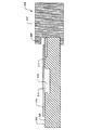
図3、図4、および図5は、本発明の例示的な実施の形態に基づく流体サンプル中の被検体をモニタリングするためのマイクロ流体の分析システム300の簡単化された模式図である。マイクロ流体の分析システム300は、分析モジュール302および電気装置304(例えば、メーターおよび/または電源)を含んでいる。
3, 4 and 5 are simplified schematic diagrams of a
分析モジュール302は、上面308を備えた絶縁基板306を含んでいる。上面308は内部にマイクロチャネル310を含んでいる。分析モジュール302は、絶縁基板306の上面308に配置された3個の導電性接触パッド312、マイクロチャネル310の上に配置された3個の電極314、電極314の各々および導電性接触パッド312の各々に接続された導電性トレース316、およびラミネート層318をも含んでいる。ラミネート層318は、電極314、導電性トレース316、および、絶縁基板306の上面308の一部の上に配置されている。
The
電気装置304は、3個のばね接触部320(そのうちの一つが図5に示されている。)およびシャーシ322を含んでいる(図5を参照のこと)。マイクロ流体の分析システム300の導電性接触パッド312は、ばね接触部320を介して電気装置304と電気的に接続するためのアクセス可能な露出面324および露出面326を含んでいる。
The
絶縁基板306は、当業者に知られた任意の適切な材料で作られていてよい。例えば、絶縁基板306は、ポリスチレン、ポリカーボネート、ポリメチルメタクリレート、ポリエステル、および、それらの任意の組み合わせなどの絶縁ポリマーで作られていてよい。電気装置および導電性接触パッドを電気的に接続できるようにするために、絶縁基板が本質的に非圧縮性で電気装置に挿入するための十分な剛性を有していることがとりわけ有益である。絶縁基板306は、任意の適切な厚さであってよく、典型的には約2mmの厚さである。
Insulating
導電性接触パッド312は、例えば、以下に記載される導電性インクおよび導電性顔料(例えば、射出成形法および印刷法で用いるのに適したグラファイト、白金、金、および、銀が添加されたポリマー)などの当業者に知られた任意の適切な導電性材料で作られていてよい。
The
導電性接触パッドは、任意の適切な厚さであってよい。しかし、電気装置を頑健かつ強固に接続できるようにするためには、導電性接触パッドの厚さは、5μmから5mmまでの範囲内にあるのが有益であり、約50μmの厚さがより好ましい。これに関しては、導電性接触パッドの厚さを電極または導電性トレースよりもかなり厚くして、電極および電気装置の(導電性トレースおよび導電性接触パッドを介した)頑健かつ強固な接続ができるようにし、同時に電極および導電性トレースを比較的薄くできることが注目されなければならない。 The conductive contact pad may be any suitable thickness. However, in order to be able to connect the electrical device robustly and firmly, it is beneficial that the thickness of the conductive contact pad is in the range of 5 μm to 5 mm, more preferably about 50 μm. . In this regard, the thickness of the conductive contact pad is much thicker than the electrode or conductive trace so that a robust and strong connection (via the conductive trace and conductive contact pad) of the electrode and electrical device is possible. At the same time, it should be noted that the electrodes and conductive traces can be relatively thin.
電極314および導電性トレース316も、以下に限定されないが、写真印刷法、スクリーン印刷法、および、フレキソ印刷法で通常用いられている導電性材料などの任意の適切な材料で作られていてよい。炭素、貴金属(例えば、金、白金、および、パラジウム)、貴金属の合金、だけでなく、電位差を形成する(potential−forming)金属酸化物および金属塩が、電極および導電性トレースのための材料に含まれる成分の例である。導電性インク(例えば、アメリカ合衆国ミシガン州48060ポート・ヒューロン(Port Huron)、ワシントンアベニュー(Washington Ave)1600のアチェソン・コロイズ・カンパニー(Acheson Colloids Company)からエレクトロダグ418SS(Electrodag(登録商標)418 SS)として市販されている銀導電性インク)が電極314および導電性トレース316を形成するために用いられてよい。電極314および導電性トレース316の典型的な厚さは、例えば、20μmである。
複数の電極がある場合では、各電極は、国際特許出願第PCT/US97/02165号(1997年8月21日にWO97/30344号として公開された。)に記載された導電性インクのような同じ導電性インクを用いて形成されていてよく、または、電極の各々に対して望ましいさまざまな特性を与える別々の導電性インクを用いて形成されていてもよい。 In the case of multiple electrodes, each electrode is like a conductive ink described in International Patent Application No. PCT / US97 / 02165 (published as WO 97/30344 on August 21, 1997). It may be formed using the same conductive ink, or may be formed using separate conductive inks that provide various desirable properties for each of the electrodes.
ラミネート層318も、以下に限定されないが、ポリスチレン、ポリカーボネート、ポリメチルメタクリレート、およびポリエステルなどの当業者に知られた任意の適切な材料で作られていてよい。本発明の実施の形態に基づくマイクロ流体の分析システムの製造は、ラミネート層318がしなやかなおよび/または曲げやすいシートの形状である場合に、簡単化できる。例えば、ラミネート層318は、実質的に5μmから実質的に500μmまでの範囲内の厚みのしなやかなシートであってよい。これに関しては、約50μmの厚さのラミネート層が製造を容易にすることに関して有益であることが見出されている。ラミネート層318は、典型的には、絶縁基板306よりも薄く、分析モジュール302の製造中に熱がラミネート層318から絶縁基板306に容易に伝わるよう十分に薄い。
本質的に液密および/または気密なマイクロチャネルは、マイクロ流体の分析システム300で、(i)マイクロチャネル310が本質的に液密および/または気密になるように、ラミネート層318が絶縁基板306の上面308の一部と融合しているとき、および/または、(ii)マイクロチャネル310が本質的に液密および/または気密になるように、電極314および/または導電性トレース316を絶縁基板306の上面308と融合させたとき、達成できる。そのような融合した構造を得るための例示的な方法が、以下に詳細に記載される。
Essentially liquid-tight and / or air-tight microchannels are
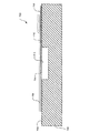
図6は、3個のばね接触部320’(そのうちの一つが図6で図示されている。)およびシャーシ322’を含む別の電気装置304’に接続されたマイクロ流体の分析システム300の分析モジュール302を示している(図6を参照のこと)。図6は、アクセス可能な露出面326と結合したばね接触部320’を示している。
FIG. 6 shows an analysis of a
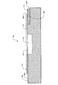
図3、図4、図5、および図6の実施の形態では、導電性接触パッド312は、上面308の凹部328内に配置されている。導電性接触パッド312を絶縁基板306の上面の凹部に配置することによって、導電性接触パッド312は、電極および導電性トレースの厚みより大きい厚みで容易に形成でき、電気装置を導電性接触パッドの上面(アクセス可能な露出面324など)および側面(例えば、アクセス可能な露出面326)の何れからでも頑健かつ強固に結合できるようになる。しかし、図7は、導電性接触パッドが絶縁基板の本質的に平坦な上面に配置されている別の構成を示している。図7は、本発明に基づくマイクロ流体の分析システムの分析モジュール700を示している。分析モジュール700は、上面708を備えた絶縁基板706を含んでいる。上面708はマイクロチャネル710を有している。
In the embodiment of FIGS. 3, 4, 5, and 6, the
分析モジュール700も、絶縁基板706の上面に配置された導電性接触パッド712、マイクロチャネル710の上に配置された電極714、電極714および導電性接触パッド712に接続された導電性トレース716、および、ラミネート層718を含んでいる。ラミネート層718は、電極714、導電性トレース716、および絶縁基板706の上面708の一部の上に配置されている。
The
本発明の開示を知ると、当業者は、本発明に基づくマイクロ流体の分析システムの分析モジュールが、複数のマイクロチャネル、複数の電極(例えば、複数の作用電極および基準電極)、複数の導電性トレース、および、複数の導電性接触パッドを含んでいてよいことに気づくであろう。さらに、絶縁基板およびラミネート層は任意の適切な形状であってよい。例えば、絶縁基板およびラミネート層は、円形の形状を有していて、導電性接触パッドが円形の絶縁基板の周縁部に配置されていてよい。 Knowing the disclosure of the present invention, those skilled in the art will recognize that the analysis module of the microfluidic analysis system according to the present invention comprises a plurality of microchannels, a plurality of electrodes (eg, a plurality of working and reference electrodes), a plurality of conductive It will be appreciated that a trace and a plurality of conductive contact pads may be included. Furthermore, the insulating substrate and the laminate layer may be any suitable shape. For example, the insulating substrate and the laminate layer may have a circular shape, and the conductive contact pads may be disposed on the peripheral edge of the circular insulating substrate.
図8は、マイクロ流体システム用のアクセス可能な導電性接触パッドを備えた分析モジュールを製造する方法800のステージを示すフロー図である。方法800は、ステップ810に示されているように、上面、上面内の少なくとも一つのマイクロチャネル、および、上面に配置された少なくとも一つの導電性接触パッドを備えた絶縁基板を形成する過程を含んでいる。図9Aは、そのような形成過程の結果を、絶縁基板950、絶縁基板950の上面952、マイクロチャネル954、および導電性接触パッド956として示している。
FIG. 8 is a flow diagram illustrating the stages of a
任意の適切な方法が、ステップ810を実行するために用いられてよい。例えば、マイクロチャネルは、エッチング法(etching techniques)、アブレーション法(ablation techniques)、射出成形法(injection moulding techniques)、または、熱型押法(hot embossing techniques)を用いて、絶縁基板の上面に形成されてよい。射出成形法が用いられる場合、絶縁ポリマー材料(高温および高圧の条件下で良好に成形型内に流れ込むことが知られている。)が用いられてよい。そのような絶縁ポリマー材料の例として、以下に限定されないが、ポリスチレン、ポリカーボネート、ポリメチルメタクリレート、およびポリエステルがある。さらに、導電性接触パッドは、例えば、導電性インクのスクリーン印刷によって、または、絶縁基板を形成する間に導電性接触パッドを同時に成形することによって、形成されてよい。
Any suitable method may be used to perform
図8のステップ820に記載されているように、少なくとも一つの電極および少なくとも一つの導電性トレースが底面に配置されたラミネート層が製造される。図9Aは、さらに、そのような製造過程の結果を、ラミネート層958、電極960、および導電性トレース962として示している。電極および導電性トレースは、例えば、当業者に知られた任意の適切な導電性インクによる印刷法によって、ラミネート層上に形成されてよい。
As described in
次に、方法800のステップ830で、ラミネート層が、
(1)ラミネート層の底面の少なくとも一部が、絶縁基板の上面の少なくとも一部と接着され、
(2)電極が少なくとも一つのマイクロチャネルに露出され、
(3)導電性トレースの各々が、少なくとも一つの導電性接触パッドと電気的に接触し、
(4)導電性接触パッドの少なくとも一つの表面が、露出されていて電気的に接続するためにアクセス可能な状態に留まる、
ように、絶縁基板に接着される。図9Bは、ステップ830の結果の構造を示している。
Next, at
(1) At least a part of the bottom surface of the laminate layer is bonded to at least a part of the top surface of the insulating substrate;
(2) the electrode is exposed to at least one microchannel;
(3) each of the conductive traces is in electrical contact with at least one conductive contact pad;
(4) at least one surface of the conductive contact pad is exposed and remains accessible for electrical connection;
In this way, it is adhered to the insulating substrate. FIG. 9B shows the resulting structure of
接着ステップ830の間、ラミネート層は、少なくとも一つのマイクロチャネルが本質的に液密、または、さらに本質的に気密になるように、絶縁基板の上面の一部と融合される。そのような融合は、十分な熱および/または圧力を加えて、ラミネート層および絶縁基板の局部的な軟化および/または溶融を起こすことによって達成される。熱および/または圧力は、例えば、加熱ローラによって加えられる。以下に拘束されないが、そのような融合は物理的な接着を原因とするものであって、化学的な接着を原因とするものではないこと、および、融合は、溶融状態のラミネート層および絶縁基板の材料の間の表面のぬれ(surface wetting)、および、固体状態での「機械的な定着(mechanical keying)」の結果であることが前提とされている。機械的な定着は、一方の材料が、第2の材料内に存在するまたは第2の材料内で発達した空隙内に物理的に侵入することを含む機構によって、2つの材料の表面が結合することを意味している。
During the
融合および液密および/または気密なマイクロチャネルの形成を可能にするためには、ラミネート層および絶縁基板の溶融特性が予め決められていなければならない。例えば、ラミネート層および絶縁基板の表面が、ラミネート層および絶縁基板の界面の十分なぬれが起こり、続いてラミネート層および絶縁基板の溶融部分の流れ込みおよび混合が起こるように、接着ステップの間に本質的に同時に溶融状態になることが有益である。その後の冷却によって、液密および/または気密なマイクロチャネルを形成するような形態でその上にラミネート層が配置された絶縁基板の一部に融合されたラミネート層が製造される。 In order to allow fusion and formation of liquid-tight and / or air-tight microchannels, the melting properties of the laminate layer and the insulating substrate must be predetermined. For example, the surface of the laminate layer and the insulating substrate is essential during the bonding step so that sufficient wetting of the interface between the laminate layer and the insulating substrate occurs, followed by the flow and mixing of the molten portion of the laminate layer and insulating substrate. It is beneficial to simultaneously enter a molten state. Subsequent cooling produces a laminate layer fused to a portion of the insulating substrate on which the laminate layer is disposed in a form that forms a liquid-tight and / or air-tight microchannel.
ラミネート層および絶縁基板の両方がポリスチレンで形成されている場合、融合は、例えば3秒間に亘る3750.3トル(5バール)の圧力および120℃の温度で生ずる。液密、または、さらに気密なマイクロチャネルの形成をさらに強化するために、接着ステップは、導電性トレースおよび/または電極が絶縁基板の上面と融合するように、実施されてもよい。そのような場合には、導電性トレース(および/または電極)が作られる材料は、ラミネート層および絶縁基板の融合と同じ圧力、温度、および時間の条件下で絶縁層と融合するように、予め決められている。しかし、導電性トレース(および/または電極)が形成される材料は、接着ステップの間に重要な定義(significant definition)を失ってはならない。 When both the laminate layer and the insulating substrate are formed of polystyrene, fusion occurs at a pressure of, for example, 3750.3 Torr (5 bar) for 3 seconds and a temperature of 120 ° C. In order to further enhance the formation of liquid-tight or air-tight microchannels, the bonding step may be performed such that the conductive traces and / or electrodes fuse with the top surface of the insulating substrate. In such cases, the material from which the conductive traces (and / or electrodes) are made is pre-adhered to fuse with the insulating layer under the same pressure, temperature, and time conditions as the laminate layer and insulating substrate. It has been decided. However, the material from which the conductive traces (and / or electrodes) are formed must not lose a significant definition during the bonding step.
さらに、導電性トレースおよび導電性接触パッドの電気的な接続を強化するために、導電性トレースおよび導電性接触パッドは、接着ステップの間に融合する材料(例えば、過剰な導電性顔料を含む材料)で作られていてよい。しかし、導電性トレースおよび導電性接触パッドの電気的な接続は、接着ステップの間に形成された物理的な機械的接触によって形成されてもよい。 Further, in order to enhance the electrical connection of the conductive traces and conductive contact pads, the conductive traces and conductive contact pads are made of a material that fuses during the bonding step (eg, a material that contains excess conductive pigment). ). However, the electrical connection between the conductive traces and the conductive contact pads may be formed by physical mechanical contact formed during the bonding step.
接着ステップの典型的な条件は、例えば、80℃から200℃までの範囲内の温度、実質的に375.03トル(0.5バール)から実質的に7500.6トル(10バール)までの範囲内の圧力、および、実質的に0.5秒から実質的に5秒までの範囲内の期間である。 Typical conditions for the bonding step are, for example, temperatures in the range of 80 ° C. to 200 ° C., substantially from 375.03 Torr (0.5 bar) to substantially 7500.6 Torr (10 bar). A pressure in the range and a period in the range from substantially 0.5 seconds to substantially 5 seconds.
〔実施例−分析モジュールの製造〕
本発明に基づくマイクロ流体の分析装置のある実施の形態が、ポリスチレン材料(すなわち、ドイツ国ルードビッヒシャフェン(Ludwigshafen)D−67056のビー・エー・エス・エフ・アクティエンゲゼルシャフト・ビジネス・ユニット・ポリスチレン(BASF Aktiengesellschaft, Business Unit Polystyrene)から市販されているポリスチロール144C(Polystyrol 144C))で形成された絶縁基板と、別のポリスチレン材料(すなわち、ドイツ国ノーデンハム(Nordenham)26954、ノードドイッチェ・ゼーカベルベルケ(Norddeutsche Seekabelwerke)のエヌ・エス・ダブリュー・クンスツストッフテヒニーク(NSW Kunststofftechnik)から市販されているノーフレックス・フィルム(Norflex(登録商標) Film))で形成されたラミネート層とを用いて、製造された。
[Example-Production of analysis module]
One embodiment of a microfluidic analyzer according to the present invention is a polystyrene material (i.e., BSF Actiengezel shaft business unit polystyrene of Ludwigshafen D-67056, Germany). (Polystyrene 144C (Polystyrene 144C) commercially available from BASF Aktiengesellschaft), another polystyrene material (ie, Nordenham 26954, Nord SE Kabelwelke) NS W Kunststoff Tehnik By using a laminate layer formed by a no flex film commercially available from NSW Kunststofftechnik) (Norflex (TM) Film)), were prepared.
電極および導電性トレースが、導電性インクを用いて、ラミネート層に印刷された。さらに、導電性接触パッドが、同じ導電性インクを用いて、絶縁基板に印刷された。導電性トレース、導電性接触パッド、および電極を印刷するのに用いられた導電性インクは、以下の質量パーセントの組成を有していた。
質量比が1:9の白金および炭素を含有する超微粉末(例えば、イギリス国SG8 6NT、サウス・ケンブリッジシェア(South Cambridgeshire)、メルドレス(Meldreth)、ノース・エンド(North End)、ユニット1Aロング・バーン(Unit 1A Long Barn)のエム・シー・エー・サービシス(MCA Services)から入手可能なMCA 20V 白金炭素(platinized carbon))を18.5%、
ポリビスフェノールA−コ−エピクロロヒドリン−グリシジル・エンドキャップポリマー(poly(bisphenol A-co-epichlorohydrin)-glycidyl end capped polymer:例えば、オランダ国3190ANホーフリート・ライト(Hoogvliet Rt)ピーオーボックス606のレゾリューション・ユアロップ・ビー・ブイ(Resolution Europe BV)、レゾリューション・エンハンスト・プロダクツ(Resolution Enhanced Products)から入手可能なエピコート1055(Epikote(商標)1055))を19.0%、および、
メチルカルビトール(ジエチレングリコールモノメチルエーテル)溶剤(ベルギー国2650エデゲム(Edegem)、プリンスボーデビィンラーン(Prins Boudewijnlaan)41のダウ・ベネルクス・ビー・ブイ(Dow Benelux B. V.)から入手された。)を62.5%
Electrodes and conductive traces were printed on the laminate layer using conductive ink. In addition, conductive contact pads were printed on the insulating substrate using the same conductive ink. The conductive ink used to print the conductive traces, conductive contact pads, and electrodes had the following mass percent composition:
Ultra fine powder containing platinum and carbon in a mass ratio of 1: 9 (eg, SG86NT, UK, South Cambridgeshire, Meldreth, North End, Unit 1A Long 18.5% of MCA 20V platinumized carbon available from MCA Services of Unit 1A Long Barn,
Poly (bisphenol A-co-epichlorohydrin) -glycidyl end capped polymer: For example, 3190AN Hoogvliet Rt Peobox 606, The Netherlands 19.0% of Resolution Europe BV, Epicoat 1055 (Epicote ™ 1055) available from Resolution Enhanced Products, and
62.5 Methyl carbitol (diethylene glycol monomethyl ether) solvent (obtained from Dow Benelux BV, 2650 Edegem, Belgium, Prince Boudewijnlaan 41). %
すぐ上の詳細な導電性インクの組成は、ポリスチレン製のラミネート層およびポリスチレン製の絶縁基板に用いるのに(以下に記載されるように)とりわけ有益である。しかし、大まかに言って、導電性インクの組成は、超微粉末のポリマーに対する質量比が実質的に3:1から実質的に1:3までの範囲内に保たれる限り変えられてよい。 The detailed conductive ink composition immediately above is particularly useful (as described below) for use in polystyrene laminate layers and polystyrene insulating substrates. Broadly speaking, however, the composition of the conductive ink may be varied as long as the mass ratio of ultrafine powder to polymer is maintained within a range of substantially 3: 1 to substantially 1: 3.
本発明の開示を知ると、当業者は、導電性インク内の溶剤の百分率が、ラミネート層および/または絶縁基板に導電性インクを塗付するのに用いられる方法(例えば、スプレー塗装(spray coating)、熱型押(hot embossing)、および、フレキソ印刷(flexographic printing))に合わせて変えることができることに気づくであろう。さらに、例えば、アルコール系溶剤(alcohols)、メチルエチルケトン、ブチルグリコール(butyl glycol)、ベンジルアセテート、エチレングリコールジアセテート、イソホロン、および、芳香族炭化水素系溶剤などの任意の適切な溶剤が、メチルカルビトール(ジエチレングリコールモノメチルエーテル)の代わりに用いられてもよい。 Knowing the disclosure of the present invention, those skilled in the art will recognize that the percentage of solvent in the conductive ink is such that the method used to apply the conductive ink to the laminate layer and / or the insulating substrate (e.g., spray coating). ), Hot embossing, and flexographic printing will be noticed. In addition, any suitable solvent such as, for example, alcohol solvents, methyl ethyl ketone, butyl glycol, benzyl acetate, ethylene glycol diacetate, isophorone, and aromatic hydrocarbon solvents may be methyl carbitol. (Diethylene glycol monomethyl ether) may be used instead.
次に、絶縁基板が、ラミネート層および絶縁基板の軟化および融合が起こるように加えられた温度および圧力の条件下でラミネート層に接着された。温度および圧力は、ラミネート層および絶縁基板を30mm/秒から3mm/秒までの範囲内の速度で加熱ローラに通すことで、ラミネート層および絶縁基板に加えられた。 Next, the insulating substrate was adhered to the laminate layer under conditions of temperature and pressure applied so that softening and fusion of the laminate layer and insulating substrate occurred. Temperature and pressure were applied to the laminate layer and insulating substrate by passing the laminate layer and insulating substrate through a heated roller at a speed in the range of 30 mm / second to 3 mm / second.
さらに、温度および圧力は、導電性インクの軟化、導電性インクと絶縁基板の融合、および、導電性インクとラミネート層の融合を起こすのに十分であった。そのような軟化および融合にもかかわらず、導電性インクはその導電特性を保持していた。したがって、上記導電性インクは可融性の導電性インクとも呼ばれる。 Furthermore, the temperature and pressure were sufficient to cause softening of the conductive ink, fusion of the conductive ink and the insulating substrate, and fusion of the conductive ink and the laminate layer. Despite such softening and coalescence, the conductive ink retained its conductive properties. Therefore, the conductive ink is also called fusible conductive ink.
接着ステップの間に用いられた温度は、典型的には、80℃から150℃までの範囲内にあり、より詳しく言うと、実質的に120℃であり、接着ステップの間に用いられた圧力は、典型的には750.06トル(1バール)から7500.6トル(10バール)までの範囲内にあり、より詳しく言うと、実質的に3750.3トル(5バール)であった。 The temperature used during the bonding step is typically in the range of 80 ° C. to 150 ° C., more specifically, substantially 120 ° C., and the pressure used during the bonding step. Was typically in the range of 750.06 torr (1 bar) to 7500.6 torr (10 bar), more specifically, substantially 3750.3 torr (5 bar).
接着ステップは、絶縁基板、ラミネート層、および、導電性インクの間の物理的接触の何れの点の間にも空隙を形成することなく、液密なマイクロチャネルを形成した。 The bonding step formed a liquid-tight microchannel without forming voids between any points of physical contact between the insulating substrate, the laminate layer, and the conductive ink.
最適な融合を促進するために、導電性インクの溶融点が、ラミネート層および絶縁基板の溶融点に対して+30℃から−50℃までの範囲内にあることが望ましい。さらに、導電性インクの溶融点が、絶縁基板の溶融点に対して0℃から−30℃までの範囲内にあることが望ましく、より好ましくは、導電性インクの溶融点が、絶縁基板の溶融点に対して−5℃から−15℃までの範囲内にある。これに関して、エピコート(Epikote)1055に関して報告された溶融点は、79℃から87℃までの範囲内にあり、ラミネート層および絶縁基板が形成されるポリスチレンの溶融点は90℃である。 In order to promote optimal fusion, it is desirable that the melting point of the conductive ink is in the range of + 30 ° C. to −50 ° C. with respect to the melting point of the laminate layer and the insulating substrate. Further, it is desirable that the melting point of the conductive ink is within a range from 0 ° C. to −30 ° C. with respect to the melting point of the insulating substrate, and more preferably, the melting point of the conductive ink is the melting point of the insulating substrate. It is in the range from −5 ° C. to −15 ° C. with respect to the point. In this regard, the melting point reported for Epikote 1055 is in the range of 79 ° C. to 87 ° C., and the melting point of the polystyrene on which the laminate layer and insulating substrate are formed is 90 ° C.
さらに、導電性インクから形成されたコンポーネント(例えば、電極、導電性トレース、および、導電性接触パッド)と絶縁基板またはラミネート層との融合を促進するために、絶縁基板およびラミネート層が形成される高分子材料の分子量よりも小さい分子量の成分を含む導電性インクを用いることが有益である。 In addition, insulating substrates and laminate layers are formed to facilitate fusion of components formed from conductive ink (eg, electrodes, conductive traces, and conductive contact pads) with the insulating substrate or laminate layer. It is beneficial to use a conductive ink that includes a component with a molecular weight less than the molecular weight of the polymeric material.
本明細書に記載された本発明の実施の形態のさまざまな変形が本発明を実施するにあたって用いられることもあることが理解されなければならない。特許請求の範囲が本発明の範囲を定義すること、および、特許請求の範囲の範囲内の構造およびその等価物が特許請求の範囲によって包含されることが意図されている。 It should be understood that various modifications of the embodiments of the invention described herein may be used in practicing the invention. It is intended that the claims define the scope of the invention and that structures within the scope of the claims and their equivalents be covered by the claims.
この発明の具体的な実施態様は以下の通りである。
(1)マイクロ流体の分析システムの製造に用いるための可融性の導電性インクであって、
白金および炭素を含有する超微粉末と、
ポリビスフェノールA−コ−エピクロロヒドリン−グリシジル・エンドキャップポリマー(poly(bisphenol A-co-epichlorohydrin)-glycidyl end capped polymer)と、
溶剤と、を含み、
前記超微粉末の前記ポリビスフェノールA−コ−エピクロロヒドリン−グリシジル・エンドキャップポリマーに対する比率が、3:1から1:3までの範囲内にある、
可融性の導電性インク。
(2)前記実施態様(1)記載の可融性の導電性インクであって、
前記超微粉末が、質量比が実質的に1:9の白金および炭素を含有する、
可融性の導電性インク。
(3)前記実施態様(1)記載の可融性の導電性インクであって、
前記溶剤が、メチルカルビトール(ジエチレングリコールモノメチルエーテル)(Methyl Carbitol (Diethylene Glycol Monomethyl Ether))である、
可融性の導電性インク。
(4)前記実施態様(1)記載の可融性の導電性インクであって、
前記可融性の導電性インクが、
質量比が1:9の白金および炭素を含有する超微粉末を18.5%と、
ポリビスフェノールA−コ−エピクロロヒドリン−グリシジル・エンドキャップポリマーを19.0%と、
メチルカルビトール(ジエチレングリコールモノメチルエーテル)溶剤を62.5%と、の質量百分率の組成を有する、可融性の導電性インク。
Specific embodiments of the present invention are as follows.
(1) A fusible conductive ink for use in manufacturing a microfluidic analysis system,
Ultrafine powder containing platinum and carbon;
Poly (bisphenol A-co-epichlorohydrin) -glycidyl end capped polymer;
A solvent, and
The ratio of the ultrafine powder to the polybisphenol A-co-epichlorohydrin-glycidyl endcap polymer is in the range of 3: 1 to 1: 3;
Fusible conductive ink.
(2) The fusible conductive ink according to the embodiment (1),
The ultrafine powder contains platinum and carbon having a mass ratio of substantially 1: 9;
Fusible conductive ink.
(3) The fusible conductive ink according to the embodiment (1),
The solvent is Methyl Carbitol (Diethylene Glycol Monomethyl Ether).
Fusible conductive ink.
(4) The fusible conductive ink according to the embodiment (1),
The fusible conductive ink is
18.5% of ultrafine powder containing platinum and carbon with a mass ratio of 1: 9;
19.0% polybisphenol A-co-epichlorohydrin-glycidyl endcap polymer,
A fusible conductive ink having a composition of mass percentage of 62.5% of methyl carbitol (diethylene glycol monomethyl ether) solvent.
100 システム
112 カートリッジ
114 局所コントローラモジュール
116 遠隔コントローラモジュール
118 サンプリングモジュール
120 分析モジュール
200 構成
202 第1の位置電極
204 第2の位置電極
206 電気インピーダンスメーター
208 タイマー
210 マイクロチャネル
212 分析センサ
300 マイクロ流体の分析システム
302 分析モジュール
304 電気装置
304’ 電気装置
306 絶縁基板
308 上面
310 マイクロチャネル
312 導電性接触パッド
314 電極
316 導電性トレース
318 ラミネート層
320 ばね接触部
320’ ばね接触部
322 シャーシ
322’ シャーシ
324 露出面
326 露出面
328 凹部
700 分析モジュール
706 絶縁基板
708 上面
710 マイクロチャネル
712 導電性接触パッド
714 電極
716 導電性トレース
718 ラミネート層
950 絶縁基板
952 上面
954 マイクロチャネル
956 導電性接触パッド
958 ラミネート層
960 電極
962 導電性トレース
100
Claims (4)
白金および炭素を含有する超微粉末と、
ポリビスフェノールA−コ−エピクロロヒドリン−グリシジル・エンドキャップポリマー(poly(bisphenol A-co-epichlorohydrin)-glycidyl end capped polymer)と、
溶剤と、を含み、
前記超微粉末の前記ポリビスフェノールA−コ−エピクロロヒドリン−グリシジル・エンドキャップポリマーに対する質量比が、3:1から1:3までの範囲内にある、
可融性の導電性インク。 A fusible conductive ink for use in manufacturing a microfluidic analytical system comprising:
Ultrafine powder containing platinum and carbon;
Poly (bisphenol A-co-epichlorohydrin) -glycidyl end capped polymer;
A solvent, and
The mass ratio of the ultrafine powder to the polybisphenol A-co-epichlorohydrin-glycidyl endcap polymer is in the range of 3: 1 to 1: 3;
Fusible conductive ink.
前記超微粉末が、質量比が実質的に1:9の白金および炭素を含有する、
可融性の導電性インク。 The fusible conductive ink according to claim 1,
The ultrafine powder contains platinum and carbon having a mass ratio of substantially 1: 9;
Fusible conductive ink.
前記溶剤が、メチルカルビトール(ジエチレングリコールモノメチルエーテル)(Methyl Carbitol (Diethylene Glycol Monomethyl Ether))である、
可融性の導電性インク。 The fusible conductive ink according to claim 1,
The solvent is Methyl Carbitol (Diethylene Glycol Monomethyl Ether).
Fusible conductive ink.
前記可融性の導電性インクが、
質量比が1:9の白金および炭素を含有する超微粉末を18.5%と、
ポリビスフェノールA−コ−エピクロロヒドリン−グリシジル・エンドキャップポリマーを19.0%と、
メチルカルビトール(ジエチレングリコールモノメチルエーテル)溶剤を62.5%と、の質量百分率の組成を有する、
可融性の導電性インク。 The fusible conductive ink according to claim 1,
The fusible conductive ink is
18.5% of ultrafine powder containing platinum and carbon with a mass ratio of 1: 9;
19.0% polybisphenol A-co-epichlorohydrin-glycidyl endcap polymer,
Having a mass percentage composition of 62.5% methyl carbitol (diethylene glycol monomethyl ether) solvent,
Fusible conductive ink.
Applications Claiming Priority (2)
| Application Number | Priority Date | Filing Date | Title |
|---|---|---|---|
| US10/957,470 | 2004-09-30 | ||
| US10/957,470 US7402616B2 (en) | 2004-09-30 | 2004-09-30 | Fusible conductive ink for use in manufacturing microfluidic analytical systems |
Publications (3)
| Publication Number | Publication Date |
|---|---|
| JP2006164950A JP2006164950A (en) | 2006-06-22 |
| JP2006164950A5 JP2006164950A5 (en) | 2012-12-13 |
| JP5160029B2 true JP5160029B2 (en) | 2013-03-13 |
Family
ID=35385692
Family Applications (1)
| Application Number | Title | Priority Date | Filing Date |
|---|---|---|---|
| JP2005284859A Active JP5160029B2 (en) | 2004-09-30 | 2005-09-29 | Fusible conductive inks for use in the manufacture of microfluidic analytical systems |
Country Status (12)
| Country | Link |
|---|---|
| US (1) | US7402616B2 (en) |
| EP (1) | EP1642945B1 (en) |
| JP (1) | JP5160029B2 (en) |
| KR (1) | KR20060051968A (en) |
| CN (1) | CN1754924B (en) |
| AT (1) | ATE360049T1 (en) |
| AU (1) | AU2005204325A1 (en) |
| CA (1) | CA2521587C (en) |
| DE (1) | DE602005000919T2 (en) |
| IL (1) | IL170501A (en) |
| SG (1) | SG121080A1 (en) |
| TW (1) | TWI397567B (en) |
Families Citing this family (57)
| Publication number | Priority date | Publication date | Assignee | Title |
|---|---|---|---|---|
| US6391005B1 (en) | 1998-03-30 | 2002-05-21 | Agilent Technologies, Inc. | Apparatus and method for penetration with shaft having a sensor for sensing penetration depth |
| US8641644B2 (en) | 2000-11-21 | 2014-02-04 | Sanofi-Aventis Deutschland Gmbh | Blood testing apparatus having a rotatable cartridge with multiple lancing elements and testing means |
| US9427532B2 (en) | 2001-06-12 | 2016-08-30 | Sanofi-Aventis Deutschland Gmbh | Tissue penetration device |
| CA2448790C (en) | 2001-06-12 | 2010-09-07 | Pelikan Technologies, Inc. | Electric lancet actuator |
| US9226699B2 (en) | 2002-04-19 | 2016-01-05 | Sanofi-Aventis Deutschland Gmbh | Body fluid sampling module with a continuous compression tissue interface surface |
| US7981056B2 (en) | 2002-04-19 | 2011-07-19 | Pelikan Technologies, Inc. | Methods and apparatus for lancet actuation |
| US8337419B2 (en) | 2002-04-19 | 2012-12-25 | Sanofi-Aventis Deutschland Gmbh | Tissue penetration device |
| US7025774B2 (en) | 2001-06-12 | 2006-04-11 | Pelikan Technologies, Inc. | Tissue penetration device |
| ES2336081T3 (en) | 2001-06-12 | 2010-04-08 | Pelikan Technologies Inc. | SELF-OPTIMIZATION PUNCTURE DEVICE WITH MEANS OF ADAPTATION TO TEMPORARY VARIATIONS IN CUTANEOUS PROPERTIES. |
| US7749174B2 (en) | 2001-06-12 | 2010-07-06 | Pelikan Technologies, Inc. | Method and apparatus for lancet launching device intergrated onto a blood-sampling cartridge |
| US9795747B2 (en) | 2010-06-02 | 2017-10-24 | Sanofi-Aventis Deutschland Gmbh | Methods and apparatus for lancet actuation |
| US8267870B2 (en) | 2002-04-19 | 2012-09-18 | Sanofi-Aventis Deutschland Gmbh | Method and apparatus for body fluid sampling with hybrid actuation |
| US7297122B2 (en) | 2002-04-19 | 2007-11-20 | Pelikan Technologies, Inc. | Method and apparatus for penetrating tissue |
| US7547287B2 (en) | 2002-04-19 | 2009-06-16 | Pelikan Technologies, Inc. | Method and apparatus for penetrating tissue |
| US7901362B2 (en) | 2002-04-19 | 2011-03-08 | Pelikan Technologies, Inc. | Method and apparatus for penetrating tissue |
| US8579831B2 (en) | 2002-04-19 | 2013-11-12 | Sanofi-Aventis Deutschland Gmbh | Method and apparatus for penetrating tissue |
| US7674232B2 (en) | 2002-04-19 | 2010-03-09 | Pelikan Technologies, Inc. | Method and apparatus for penetrating tissue |
| US7491178B2 (en) | 2002-04-19 | 2009-02-17 | Pelikan Technologies, Inc. | Method and apparatus for penetrating tissue |
| US9314194B2 (en) | 2002-04-19 | 2016-04-19 | Sanofi-Aventis Deutschland Gmbh | Tissue penetration device |
| US8784335B2 (en) | 2002-04-19 | 2014-07-22 | Sanofi-Aventis Deutschland Gmbh | Body fluid sampling device with a capacitive sensor |
| US7175642B2 (en) | 2002-04-19 | 2007-02-13 | Pelikan Technologies, Inc. | Methods and apparatus for lancet actuation |
| US8702624B2 (en) | 2006-09-29 | 2014-04-22 | Sanofi-Aventis Deutschland Gmbh | Analyte measurement device with a single shot actuator |
| US9248267B2 (en) | 2002-04-19 | 2016-02-02 | Sanofi-Aventis Deustchland Gmbh | Tissue penetration device |
| US7331931B2 (en) | 2002-04-19 | 2008-02-19 | Pelikan Technologies, Inc. | Method and apparatus for penetrating tissue |
| US8372016B2 (en) | 2002-04-19 | 2013-02-12 | Sanofi-Aventis Deutschland Gmbh | Method and apparatus for body fluid sampling and analyte sensing |
| US7229458B2 (en) | 2002-04-19 | 2007-06-12 | Pelikan Technologies, Inc. | Method and apparatus for penetrating tissue |
| US7909778B2 (en) | 2002-04-19 | 2011-03-22 | Pelikan Technologies, Inc. | Method and apparatus for penetrating tissue |
| US9795334B2 (en) | 2002-04-19 | 2017-10-24 | Sanofi-Aventis Deutschland Gmbh | Method and apparatus for penetrating tissue |
| US7232451B2 (en) | 2002-04-19 | 2007-06-19 | Pelikan Technologies, Inc. | Method and apparatus for penetrating tissue |
| US8221334B2 (en) | 2002-04-19 | 2012-07-17 | Sanofi-Aventis Deutschland Gmbh | Method and apparatus for penetrating tissue |
| US7976476B2 (en) | 2002-04-19 | 2011-07-12 | Pelikan Technologies, Inc. | Device and method for variable speed lancet |
| US7198606B2 (en) | 2002-04-19 | 2007-04-03 | Pelikan Technologies, Inc. | Method and apparatus for a multi-use body fluid sampling device with analyte sensing |
| US7892183B2 (en) | 2002-04-19 | 2011-02-22 | Pelikan Technologies, Inc. | Method and apparatus for body fluid sampling and analyte sensing |
| US8360992B2 (en) | 2002-04-19 | 2013-01-29 | Sanofi-Aventis Deutschland Gmbh | Method and apparatus for penetrating tissue |
| US8574895B2 (en) | 2002-12-30 | 2013-11-05 | Sanofi-Aventis Deutschland Gmbh | Method and apparatus using optical techniques to measure analyte levels |
| WO2004107975A2 (en) | 2003-05-30 | 2004-12-16 | Pelikan Technologies, Inc. | Method and apparatus for fluid injection |
| US7850621B2 (en) | 2003-06-06 | 2010-12-14 | Pelikan Technologies, Inc. | Method and apparatus for body fluid sampling and analyte sensing |
| WO2006001797A1 (en) | 2004-06-14 | 2006-01-05 | Pelikan Technologies, Inc. | Low pain penetrating |
| EP1671096A4 (en) | 2003-09-29 | 2009-09-16 | Pelikan Technologies Inc | Method and apparatus for an improved sample capture device |
| US9351680B2 (en) | 2003-10-14 | 2016-05-31 | Sanofi-Aventis Deutschland Gmbh | Method and apparatus for a variable user interface |
| US7822454B1 (en) | 2005-01-03 | 2010-10-26 | Pelikan Technologies, Inc. | Fluid sampling device with improved analyte detecting member configuration |
| WO2005065414A2 (en) | 2003-12-31 | 2005-07-21 | Pelikan Technologies, Inc. | Method and apparatus for improving fluidic flow and sample capture |
| US8828203B2 (en) | 2004-05-20 | 2014-09-09 | Sanofi-Aventis Deutschland Gmbh | Printable hydrogels for biosensors |
| EP1765194A4 (en) | 2004-06-03 | 2010-09-29 | Pelikan Technologies Inc | Method and apparatus for a fluid sampling device |
| US9775553B2 (en) | 2004-06-03 | 2017-10-03 | Sanofi-Aventis Deutschland Gmbh | Method and apparatus for a fluid sampling device |
| US8652831B2 (en) | 2004-12-30 | 2014-02-18 | Sanofi-Aventis Deutschland Gmbh | Method and apparatus for analyte measurement test time |
| EP2079547A4 (en) * | 2006-11-09 | 2010-08-04 | Gyros Patent Ab | Improved lid |
| WO2009126900A1 (en) | 2008-04-11 | 2009-10-15 | Pelikan Technologies, Inc. | Method and apparatus for analyte detecting device |
| US9375169B2 (en) | 2009-01-30 | 2016-06-28 | Sanofi-Aventis Deutschland Gmbh | Cam drive for managing disposable penetrating member actions with a single motor and motor and control system |
| WO2011085235A1 (en) | 2010-01-08 | 2011-07-14 | Abs Materials, Inc. | Porous, swellable, sol-gel derived sensor material and method for using same |
| WO2011085224A1 (en) | 2010-01-08 | 2011-07-14 | Abs Materials, Inc. | Modified sol-gel derived sorbent material and method for using same |
| WO2011100532A1 (en) | 2010-02-12 | 2011-08-18 | Abs Materials, Inc. | Sol-gel derived sorbent material containing a sorbate interactive material and method for using the same |
| WO2011162836A1 (en) | 2010-02-17 | 2011-12-29 | Abs Materials, Inc | Method for extracting a metal particulate from an aqueous solution using a sol-gel derived sorbent |
| US8965476B2 (en) | 2010-04-16 | 2015-02-24 | Sanofi-Aventis Deutschland Gmbh | Tissue penetration device |
| WO2011156663A1 (en) | 2010-06-10 | 2011-12-15 | Abs Materials,Inc | Method of treating a material using a sol-gel derived composition |
| GB2488752A (en) | 2011-02-21 | 2012-09-12 | Sony Dadc Austria Ag | Microfluidic Device |
| WO2013120908A1 (en) * | 2012-02-17 | 2013-08-22 | Sony Dadc Austria Ag | Microstructured polymer devices |
Family Cites Families (39)
| Publication number | Priority date | Publication date | Assignee | Title |
|---|---|---|---|---|
| GB8817997D0 (en) | 1988-07-28 | 1988-09-01 | Cambridge Life Sciences | Enzyme electrodes & improvements in manufacture thereof |
| US5047283A (en) | 1989-09-20 | 1991-09-10 | Ppg Industries, Inc. | Electrically conductive article |
| US6176962B1 (en) * | 1990-02-28 | 2001-01-23 | Aclara Biosciences, Inc. | Methods for fabricating enclosed microchannel structures |
| US5494562A (en) * | 1994-06-27 | 1996-02-27 | Ciba Corning Diagnostics Corp. | Electrochemical sensors |
| US5708247A (en) | 1996-02-14 | 1998-01-13 | Selfcare, Inc. | Disposable glucose test strips, and methods and compositions for making same |
| US5857983A (en) | 1996-05-17 | 1999-01-12 | Mercury Diagnostics, Inc. | Methods and apparatus for sampling body fluid |
| US5707502A (en) * | 1996-07-12 | 1998-01-13 | Chiron Diagnostics Corporation | Sensors for measuring analyte concentrations and methods of making same |
| US5906723A (en) * | 1996-08-26 | 1999-05-25 | The Regents Of The University Of California | Electrochemical detector integrated on microfabricated capillary electrophoresis chips |
| US6391622B1 (en) * | 1997-04-04 | 2002-05-21 | Caliper Technologies Corp. | Closed-loop biochemical analyzers |
| US5888390A (en) | 1997-04-30 | 1999-03-30 | Hewlett-Packard Company | Multilayer integrated assembly for effecting fluid handling functions |
| JP2001517789A (en) * | 1997-09-19 | 2001-10-09 | アクレイラ バイオサイエンシズ,インコーポレイティド | Liquid transfer device and liquid transfer method |
| EP1032824A4 (en) | 1997-10-15 | 2003-07-23 | Aclara Biosciences Inc | Laminate microstructure device and method for making same |
| US6033202A (en) * | 1998-03-27 | 2000-03-07 | Lucent Technologies Inc. | Mold for non - photolithographic fabrication of microstructures |
| US6042751A (en) * | 1998-09-17 | 2000-03-28 | E. I. Du Pont De Nemours And Company | Thick film conductor composition for use in biosensors |
| US6599408B1 (en) * | 1998-09-17 | 2003-07-29 | E. I. Du Pont De Nemours And Company | Thick film conductor composition for use in biosensors |
| US6110576A (en) * | 1998-10-16 | 2000-08-29 | Lucent Technologies Inc. | Article comprising molded circuit |
| US6503359B2 (en) * | 1999-03-05 | 2003-01-07 | Burstein Technologies, Inc. | Monomolecular adhesion methods for manufacturing microfabricated multilaminate devices |
| US6942771B1 (en) | 1999-04-21 | 2005-09-13 | Clinical Micro Sensors, Inc. | Microfluidic systems in the electrochemical detection of target analytes |
| US6593398B2 (en) * | 1999-06-29 | 2003-07-15 | Xerox Corporation | Ink compositions |
| US6878255B1 (en) | 1999-11-05 | 2005-04-12 | Arrowhead Center, Inc. | Microfluidic devices with thick-film electrochemical detection |
| JP2003517591A (en) | 1999-12-09 | 2003-05-27 | モトローラ・インコーポレイテッド | Multilayer microfluidic device for reaction of analytical samples |
| SE0000300D0 (en) | 2000-01-30 | 2000-01-30 | Amersham Pharm Biotech Ab | Microfluidic assembly, covering method for the manufacture of the assembly and the use of the assembly |
| US20020189946A1 (en) * | 2000-02-11 | 2002-12-19 | Aclara Biosciences, Inc. | Microfluidic injection and separation system and method |
| KR100446609B1 (en) * | 2000-03-17 | 2004-09-04 | 삼성전자주식회사 | Proton exchange membrane fuel cell and monopolar cell pack of direct methanol fuel cell |
| US6939451B2 (en) | 2000-09-19 | 2005-09-06 | Aclara Biosciences, Inc. | Microfluidic chip having integrated electrodes |
| GB0030929D0 (en) | 2000-12-19 | 2001-01-31 | Inverness Medical Ltd | Analyte measurement |
| ATE381599T1 (en) * | 2001-01-15 | 2008-01-15 | Seiko Epson Corp | OIL-BASED INK COMPOSITION FOR INKJET PRINTING PROCESSES AND INKJET PRINTING PROCESSES |
| US6627058B1 (en) * | 2001-01-17 | 2003-09-30 | E. I. Du Pont De Nemours And Company | Thick film conductor composition for use in biosensors |
| US6981522B2 (en) * | 2001-06-07 | 2006-01-03 | Nanostream, Inc. | Microfluidic devices with distributing inputs |
| US6729869B2 (en) * | 2001-07-16 | 2004-05-04 | Sca Hygiene Products Gmbh | Device for applying an embossing to a web of tissue paper |
| US7390463B2 (en) | 2001-09-07 | 2008-06-24 | Corning Incorporated | Microcolumn-based, high-throughput microfluidic device |
| GB0128350D0 (en) | 2001-11-27 | 2002-01-16 | Lab901 Ltd | Non-rigid apparatus for microfluidic applications |
| TW200307734A (en) * | 2002-03-20 | 2003-12-16 | Michigan Biotech Inst | Conductive polymer-based material |
| US20030203504A1 (en) * | 2002-04-26 | 2003-10-30 | John Hefti | Diffusion-based system and method for detecting and monitoring activity of biologic and chemical species |
| US20030230488A1 (en) * | 2002-06-13 | 2003-12-18 | Lawrence Lee | Microfluidic device preparation system |
| US7258673B2 (en) | 2003-06-06 | 2007-08-21 | Lifescan, Inc | Devices, systems and methods for extracting bodily fluid and monitoring an analyte therein |
| US6990849B2 (en) | 2004-03-26 | 2006-01-31 | Lifescan, Inc. | Microfluidic analytical system with position electrodes |
| US20060065532A1 (en) * | 2004-09-30 | 2006-03-30 | Matthias Stiene | Microfluidic analytical system with accessible electrically conductive contact pads |
| US20060065361A1 (en) * | 2004-09-30 | 2006-03-30 | Matthias Stiene | Process for manufacturing an analysis module with accessible electrically conductive contact pads for a microfluidic analytical system |
-
2004
- 2004-09-30 US US10/957,470 patent/US7402616B2/en active Active
-
2005
- 2005-08-25 IL IL170501A patent/IL170501A/en not_active IP Right Cessation
- 2005-08-25 SG SG200505440A patent/SG121080A1/en unknown
- 2005-08-29 AU AU2005204325A patent/AU2005204325A1/en not_active Abandoned
- 2005-09-29 EP EP05256108A patent/EP1642945B1/en not_active Not-in-force
- 2005-09-29 CA CA2521587A patent/CA2521587C/en not_active Expired - Fee Related
- 2005-09-29 CN CN2005101076583A patent/CN1754924B/en not_active Expired - Fee Related
- 2005-09-29 DE DE602005000919T patent/DE602005000919T2/en active Active
- 2005-09-29 JP JP2005284859A patent/JP5160029B2/en active Active
- 2005-09-29 TW TW094133859A patent/TWI397567B/en not_active IP Right Cessation
- 2005-09-29 AT AT05256108T patent/ATE360049T1/en not_active IP Right Cessation
- 2005-09-30 KR KR1020050092296A patent/KR20060051968A/en not_active Application Discontinuation
Also Published As
| Publication number | Publication date |
|---|---|
| TWI397567B (en) | 2013-06-01 |
| ATE360049T1 (en) | 2007-05-15 |
| EP1642945A1 (en) | 2006-04-05 |
| CA2521587A1 (en) | 2006-03-30 |
| CN1754924B (en) | 2010-06-09 |
| SG121080A1 (en) | 2006-04-26 |
| AU2005204325A1 (en) | 2006-04-13 |
| DE602005000919D1 (en) | 2007-05-31 |
| CA2521587C (en) | 2013-01-29 |
| CN1754924A (en) | 2006-04-05 |
| EP1642945B1 (en) | 2007-04-18 |
| TW200615352A (en) | 2006-05-16 |
| KR20060051968A (en) | 2006-05-19 |
| JP2006164950A (en) | 2006-06-22 |
| US20060074143A1 (en) | 2006-04-06 |
| US7402616B2 (en) | 2008-07-22 |
| DE602005000919T2 (en) | 2008-01-17 |
| IL170501A (en) | 2010-12-30 |
Similar Documents
| Publication | Publication Date | Title |
|---|---|---|
| JP5160029B2 (en) | Fusible conductive inks for use in the manufacture of microfluidic analytical systems | |
| JP2006105987A (en) | Manufacturing method of analysis module having accessible electrically conductive contact pad for microfluidic analytical system | |
| JP2006133219A (en) | Micro-fluid analytical system | |
| JP4767493B2 (en) | Electrochemical cell | |
| CN101004411B (en) | Biochip, biosensor and inspection system | |
| CA2833669C (en) | Electrochemical sensors with carrier field | |
| US20070266871A1 (en) | Diagnostic test media and methods for the manufacture thereof | |
| US20040000371A1 (en) | Embedded metallic deposits | |
| TW200815752A (en) | Methods for fabricating a biosensor with a surface texture | |
| KR20140137410A (en) | Test strip with stacked unidirectional contact | |
| KR20140137409A (en) | Test strip with stacked unidirectional contact pads and inert carrier substrate | |
| US20120160678A1 (en) | Electrode device for an electrochemical sensor chip | |
| EP1969135B1 (en) | Process of making electrodes for test sensors | |
| Huang et al. | Post-CMOS compatible microfabrication of a multi-analyte bioelectrochemical sensor array microsystem | |
| Chang et al. | Biosensor |
Legal Events
| Date | Code | Title | Description |
|---|---|---|---|
| RD04 | Notification of resignation of power of attorney |
Free format text: JAPANESE INTERMEDIATE CODE: A7424 Effective date: 20071129 |
|
| A621 | Written request for application examination |
Free format text: JAPANESE INTERMEDIATE CODE: A621 Effective date: 20080701 |
|
| RD04 | Notification of resignation of power of attorney |
Free format text: JAPANESE INTERMEDIATE CODE: A7424 Effective date: 20080926 |
|
| A977 | Report on retrieval |
Free format text: JAPANESE INTERMEDIATE CODE: A971007 Effective date: 20110714 |
|
| A131 | Notification of reasons for refusal |
Free format text: JAPANESE INTERMEDIATE CODE: A131 Effective date: 20111108 |
|
| A601 | Written request for extension of time |
Free format text: JAPANESE INTERMEDIATE CODE: A601 Effective date: 20120208 |
|
| A602 | Written permission of extension of time |
Free format text: JAPANESE INTERMEDIATE CODE: A602 Effective date: 20120213 |
|
| A521 | Request for written amendment filed |
Free format text: JAPANESE INTERMEDIATE CODE: A523 Effective date: 20120307 |
|
| A524 | Written submission of copy of amendment under article 19 pct |
Free format text: JAPANESE INTERMEDIATE CODE: A524 Effective date: 20120307 |
|
| A131 | Notification of reasons for refusal |
Free format text: JAPANESE INTERMEDIATE CODE: A131 Effective date: 20120807 |
|
| A521 | Request for written amendment filed |
Free format text: JAPANESE INTERMEDIATE CODE: A523 Effective date: 20121030 |
|
| A524 | Written submission of copy of amendment under article 19 pct |
Free format text: JAPANESE INTERMEDIATE CODE: A524 Effective date: 20121030 |
|
| TRDD | Decision of grant or rejection written | ||
| A01 | Written decision to grant a patent or to grant a registration (utility model) |
Free format text: JAPANESE INTERMEDIATE CODE: A01 Effective date: 20121127 |
|
| A61 | First payment of annual fees (during grant procedure) |
Free format text: JAPANESE INTERMEDIATE CODE: A61 Effective date: 20121212 |
|
| R150 | Certificate of patent or registration of utility model |
Ref document number: 5160029 Country of ref document: JP Free format text: JAPANESE INTERMEDIATE CODE: R150 Free format text: JAPANESE INTERMEDIATE CODE: R150 |
|
| FPAY | Renewal fee payment (event date is renewal date of database) |
Free format text: PAYMENT UNTIL: 20151221 Year of fee payment: 3 |
|
| R250 | Receipt of annual fees |
Free format text: JAPANESE INTERMEDIATE CODE: R250 |
|
| R250 | Receipt of annual fees |
Free format text: JAPANESE INTERMEDIATE CODE: R250 |
|
| R250 | Receipt of annual fees |
Free format text: JAPANESE INTERMEDIATE CODE: R250 |
|
| R250 | Receipt of annual fees |
Free format text: JAPANESE INTERMEDIATE CODE: R250 |
|
| R250 | Receipt of annual fees |
Free format text: JAPANESE INTERMEDIATE CODE: R250 |
|
| R250 | Receipt of annual fees |
Free format text: JAPANESE INTERMEDIATE CODE: R250 |
|
| R250 | Receipt of annual fees |
Free format text: JAPANESE INTERMEDIATE CODE: R250 |
|
| R250 | Receipt of annual fees |
Free format text: JAPANESE INTERMEDIATE CODE: R250 |
|
| R250 | Receipt of annual fees |
Free format text: JAPANESE INTERMEDIATE CODE: R250 |