JP5158552B1 - Microscope and inspection device - Google Patents
Microscope and inspection device Download PDFInfo
- Publication number
- JP5158552B1 JP5158552B1 JP2012048949A JP2012048949A JP5158552B1 JP 5158552 B1 JP5158552 B1 JP 5158552B1 JP 2012048949 A JP2012048949 A JP 2012048949A JP 2012048949 A JP2012048949 A JP 2012048949A JP 5158552 B1 JP5158552 B1 JP 5158552B1
- Authority
- JP
- Japan
- Prior art keywords
- light
- illumination
- sample
- light source
- source device
- Prior art date
- Legal status (The legal status is an assumption and is not a legal conclusion. Google has not performed a legal analysis and makes no representation as to the accuracy of the status listed.)
- Expired - Fee Related
Links
Images


Classifications
-
- G—PHYSICS
- G02—OPTICS
- G02B—OPTICAL ELEMENTS, SYSTEMS OR APPARATUS
- G02B21/00—Microscopes
- G02B21/06—Means for illuminating specimens
-
- G—PHYSICS
- G02—OPTICS
- G02B—OPTICAL ELEMENTS, SYSTEMS OR APPARATUS
- G02B21/00—Microscopes
- G02B21/0004—Microscopes specially adapted for specific applications
- G02B21/0092—Polarisation microscopes
-
- G—PHYSICS
- G01—MEASURING; TESTING
- G01N—INVESTIGATING OR ANALYSING MATERIALS BY DETERMINING THEIR CHEMICAL OR PHYSICAL PROPERTIES
- G01N21/00—Investigating or analysing materials by the use of optical means, i.e. using sub-millimetre waves, infrared, visible or ultraviolet light
- G01N21/84—Systems specially adapted for particular applications
- G01N21/88—Investigating the presence of flaws or contamination
- G01N21/95—Investigating the presence of flaws or contamination characterised by the material or shape of the object to be examined
- G01N21/9501—Semiconductor wafers
- G01N21/9505—Wafer internal defects, e.g. microcracks
-
- G—PHYSICS
- G02—OPTICS
- G02B—OPTICAL ELEMENTS, SYSTEMS OR APPARATUS
- G02B21/00—Microscopes
- G02B21/06—Means for illuminating specimens
- G02B21/08—Condensers
- G02B21/10—Condensers affording dark-field illumination
-
- G—PHYSICS
- G02—OPTICS
- G02B—OPTICAL ELEMENTS, SYSTEMS OR APPARATUS
- G02B6/00—Light guides; Structural details of arrangements comprising light guides and other optical elements, e.g. couplings
- G02B6/0001—Light guides; Structural details of arrangements comprising light guides and other optical elements, e.g. couplings specially adapted for lighting devices or systems
- G02B6/0005—Light guides; Structural details of arrangements comprising light guides and other optical elements, e.g. couplings specially adapted for lighting devices or systems the light guides being of the fibre type
- G02B6/0008—Light guides; Structural details of arrangements comprising light guides and other optical elements, e.g. couplings specially adapted for lighting devices or systems the light guides being of the fibre type the light being emitted at the end of the fibre
Landscapes
- Physics & Mathematics (AREA)
- General Physics & Mathematics (AREA)
- Chemical & Material Sciences (AREA)
- Analytical Chemistry (AREA)
- Optics & Photonics (AREA)
- Life Sciences & Earth Sciences (AREA)
- Health & Medical Sciences (AREA)
- Biochemistry (AREA)
- General Health & Medical Sciences (AREA)
- Immunology (AREA)
- Pathology (AREA)
- Investigating Materials By The Use Of Optical Means Adapted For Particular Applications (AREA)
- Microscoopes, Condenser (AREA)
Abstract
【課題】開口数の大きな対物レンズを用いることができ、試料の内部構造による欠陥を高分解能で検査できる顕微鏡及び検査装置を実現する。
【解決手段】直線偏光した照明光を発生する光源装置(20a〜20c)を用い、光源装置から出射した照明光を偏波面保存ファイバ(10a〜10d)を介してP偏光した照明光として試料(1)の表面に向けて投射する。試料表面に対する照明光の入射角は試料に固有のブリュースター角に設定する。P偏光した照明光がブリュースター角に等しい入射角で試料表面に入射すると、表面反射率は零であるため、表面反射のない照明光学系が構成される。さらに、シリコン材料のブリュースター角は75°と比較的大きい角度であるため、対物レンズに対する空間的な制約が緩和され、開口数の大きな対物レンズを用いて散乱光を集光することが可能になる。
【選択図】図1An objective of the present invention is to realize a microscope and inspection apparatus capable of inspecting a defect due to the internal structure of a sample with high resolution by using an objective lens with a large numerical aperture.
A light source device (20a to 20c) for generating linearly polarized illumination light, and a sample (the illumination light emitted from the light source device as P-polarized illumination light through polarization maintaining fibers (10a to 10d) Project toward the surface of 1). The incident angle of the illumination light on the sample surface is set to the Brewster's angle specific to the sample. When the P-polarized illumination light is incident on the sample surface at an incident angle equal to the Brewster's angle, the surface reflectance is zero, so that an illumination optical system without surface reflection is configured. Furthermore, since Brewster's angle of silicon material is a relatively large angle of 75 °, spatial restrictions on the objective lens are relaxed, and scattered light can be collected using the objective lens with a large numerical aperture. Become.
[Selected figure] Figure 1
Description
本発明は、各種試料の内部構造を外部から観察し又は検査するのに好適な顕微鏡に関するものである。
また、本発明は暗視野照明を利用してシリコン基板に形成された半導体層の内部又は半導体層に形成された孔又は溝に存在する欠陥を検出するのに好適な検査装置に関するものである。
The present invention relates to a microscope suitable for observing or inspecting the internal structure of various samples from the outside.
The present invention also relates to an inspection apparatus suitable for detecting a defect present in a hole or a groove formed in a semiconductor layer formed in a silicon substrate or in a semiconductor layer using dark field illumination.
半導体デバイスの製造プロセスにおいては、トレンチアイソレーションを利用した各種デバイスが開発されている。例えば、高耐圧MOSFETとして、トレンチゲート構造を有するMOSFETが開発されている。また、CMOSセンサやCCDセンサ等の撮像素子においても、各受光素子を分離するようにトレンチが形成され、隣接する画素間のクロストークが防止されている。一方、トレンチの深さはデバイスの性能や製造の歩留りに強い影響を与え、例えば、CMOSセンサにおいては、不完全なトレンチが形成された場合、隣接する画素間の電荷の漏洩が大きくなり、撮像される画像品質に悪影響を及ぼすおそれがある。 In the manufacturing process of semiconductor devices, various devices utilizing trench isolation have been developed. For example, a MOSFET having a trench gate structure has been developed as a high voltage MOSFET. In addition, also in an imaging device such as a CMOS sensor or a CCD sensor, a trench is formed so as to separate light receiving elements, and crosstalk between adjacent pixels is prevented. On the other hand, the depth of the trench has a strong influence on the device performance and the manufacturing yield. For example, in the case of a CMOS sensor, if an incomplete trench is formed, the charge leakage between adjacent pixels becomes large, and imaging Image quality may be adversely affected.
メモリ素子が積層されたフラッシュメモリが開発されている。この積層型のフラッシュメモリの製造工程においては、シリコン基板に半導体層及び酸化シリコン層が交互に積層されて多層膜構造体が形成されている。そして、多層膜構造体に柱状トランジスタを形成するための孔が形成され、形成された孔の内部に半導体材料が埋め込まれている。このような積層型のフラッシュメモリの製造工程においても、多層膜構造体中に形成される孔がエッチング不良等に起因して不完全な場合、或いは孔の直径が局所的に狭く形成された場合又は孔の内部に異物が存在する場合、不完全な柱状トランジスタが形成され、同様に製造の歩留りが低下する不具合が生じてしまう。従って、各種半導体デバイスの製造工程中に半導体層が正常に形成されているか否か及び各種の孔や溝が正常に形成されているか否かを検査する顕微鏡及び検査装置の開発が強く要請されている。特に半導体層及び半導体層に形成された孔や溝等含む半導体層の内部に存在する欠陥を半導体基板の外部から高分解能で検出できる検査装置の開発が強く要請されている。 Flash memory in which memory elements are stacked has been developed. In the manufacturing process of the stacked flash memory, semiconductor layers and silicon oxide layers are alternately stacked on a silicon substrate to form a multilayer film structure. Then, a hole for forming a columnar transistor is formed in the multilayer film structure, and a semiconductor material is embedded in the formed hole. Also in the manufacturing process of such a stacked flash memory, when the holes formed in the multilayer film structure are incomplete due to an etching failure or the like, or the diameter of the holes is formed locally narrow. Alternatively, if foreign matter is present inside the hole, an incomplete columnar transistor is formed, which similarly causes a problem that the manufacturing yield is lowered. Therefore, there is a strong demand for development of a microscope and an inspection apparatus for inspecting whether the semiconductor layer is properly formed and whether various holes and grooves are normally formed during the manufacturing process of various semiconductor devices. There is. In particular, development of an inspection apparatus capable of detecting a defect existing inside a semiconductor layer including a semiconductor layer and a semiconductor layer including a hole and a groove formed in the semiconductor layer from the outside of the semiconductor substrate with high resolution is strongly demanded.
従来、半導体デバイスの製造プロセスにおいて、暗視野顕微鏡を用いて半導体基板を観察し又は検査する装置が知られている(例えば、特許文献1参照)。この既知の暗視野顕微鏡においては、輪帯状の照明光を用いて試料表面を照明するため、対物レンズが二重筒状構造にされ、内側の空間に対物レンズを含む結像系の光路が形成され、対物レンズの光路の外側に照明光を伝搬させるための光路が形成されている。そして、試料表面からの散乱光が対物レンズを介して検出されている。 Conventionally, an apparatus for observing or inspecting a semiconductor substrate using a dark field microscope in a manufacturing process of a semiconductor device is known (see, for example, Patent Document 1). In this known dark-field microscope, in order to illuminate the sample surface with ring-shaped illumination light, the objective lens is formed into a double cylindrical structure, and the optical path of the imaging system including the objective lens is formed in the inner space. An optical path for propagating the illumination light is formed outside the optical path of the objective lens. Then, the scattered light from the sample surface is detected through the objective lens.
また、波長の異なる照明光で試料表面を照明する顕微鏡も既知である(例えば、特許文献2参照)。この既知の顕微鏡では、結像光学系の光路の外側に波長の異なる照明光をそれぞれ発生する光源を複数組配置し、偏向用のレンズ素子を介して対物レンズの光軸を含む照明領域に波長の異なる照明光が投射されている。また、照明光の波長として、可視光域及び近赤外域の照明光が用いられている。
上述した暗視野顕微鏡においては、対物レンズが二重筒状構造にされているため、対物レンズを収納する空間が制限されている。このため、開口数の大きな対物レンズが使用できず、高分解能の欠陥検査を行うには限界があった。また、試料表面における表面反射が強く発生し、その結果フレアの光量が大き過ぎ、微弱な散乱光を高精度に検出するのに限界があった。 In the dark field microscope described above, since the objective lens has a double cylindrical structure, the space for housing the objective lens is limited. For this reason, an objective lens with a large numerical aperture can not be used, and there is a limit in performing high resolution defect inspection. In addition, surface reflection on the surface of the sample occurs strongly, and as a result, the amount of light of the flare is too large, and there is a limit in detecting weak scattered light with high accuracy.
さらに、表面反射による損失が大きいため、試料の内部に進入する照明光の光量の割合が低く、半導体層に形成された孔や溝に存在する欠陥から発生する散乱光の強度が微弱であり、半導体層に形成された孔や溝に存在する欠陥の検出精度が低下する不具合も生じていた。さらに、従来の暗視野顕微鏡は、試料表面からの散乱光の検出を主目的としており、試料の外部から試料の内部構造の欠陥を検出することについて言及されていない。 Furthermore, since the loss due to surface reflection is large, the ratio of the light amount of the illumination light entering the inside of the sample is low, and the intensity of the scattered light generated from the defects present in the holes and grooves formed in the semiconductor layer is weak. The defect that the detection accuracy of the defect which exists in the hole and the groove which were formed in the semiconductor layer fell also occurred. Furthermore, conventional dark-field microscopes are mainly intended for the detection of scattered light from the sample surface, and no mention is made of the detection of defects in the internal structure of the sample from the outside of the sample.
本発明の目的は、開口数の大きな対物レンズを用いることができ、試料の内部に存在する欠陥を高分解能で検出できる顕微鏡及び検査装置を実現することにある。
さらに、本発明の別の目的は、表面反射による損失が小さく、フレアが少なく且つシリコン基体の内部に進入する照明光が増大した顕微鏡及び検査装置を提供することにある。
An object of the present invention is to realize a microscope and an inspection apparatus which can use an objective lens having a large numerical aperture and can detect a defect existing inside a sample with high resolution.
Furthermore, another object of the present invention is to provide a microscope and inspection apparatus in which the loss due to surface reflection is small, the flare is small, and the illumination light entering the interior of the silicon substrate is increased.
本発明による顕微鏡は、直線偏光した光ビームを発生する光源装置と、
光源装置に光学的に結合され、光源装置から出射し直線偏光した光ビームを試料表面の照明エリアにP偏光した照明ビームとして投射する偏波面保存ファイバと、
光軸が前記試料表面に対して直交するように配置され、試料から発生した散乱光を集光する対物レンズと、
対物レンズにより集光された散乱光を受光する光検出手段とを有し、
前記偏波面保存ファイバは、試料表面に対してブリュースター角にほぼ等しい入射角でP偏光した照明ビームを投射することを特徴とする。
The microscope according to the invention comprises a light source device for generating a linearly polarized light beam;
A polarization maintaining fiber which is optically coupled to the light source device and projects the linearly polarized light beam emitted from the light source device onto the illumination area of the sample surface as a P-polarized illumination beam;
An objective lens disposed so that the optical axis is orthogonal to the surface of the sample and collecting scattered light generated from the sample;
And light detection means for receiving scattered light collected by the objective lens,
The polarization maintaining fiber is characterized in that it projects a P-polarized illumination beam at an incident angle substantially equal to Brewster's angle with respect to the sample surface.
本発明では、照明光としてP偏光した照明光を用い、P偏光した照明光を試料表面に対してブリュースター角に等しい入射角で投射する。後述するように、試料表面に対してP偏光した照明光をブリュースター角に等しい入射角で投射すれば、表面反射率はほぼ零になるため、表面反射がほとんど発生せず、大部分の照明光が試料の内部に透過する照明系が実現される。さらに、例えばシリコン材料のブリュースター角は、波長が800nm付近の照明光の場合75°付近であるため、照明ビームは比較的大きな入射角で試料表面に投射される。この結果、対物レンズに対する空間的な制約が緩和されるので、開口数の大きな対物レンズを用いることが可能になり、高分解能の欠陥検査が可能になる。さらに重要なことは、試料表面に対してブリュースター角に等しい入射角で照明すれば、試料から出射した正反射光は対物レンズの集光範囲から外れるため、暗視野照明光学系が構成される。この結果、試料の内部構造体で発生した散乱光の強度が微弱であっても散乱光を高精度に検出することが可能になり、開口数の大きな対物レンズを用いることと相まって、一層高精度な欠陥検出を行うことが可能になる。 In the present invention, P-polarized illumination light is used as the illumination light, and the P-polarized illumination light is projected onto the sample surface at an incident angle equal to the Brewster's angle. As described later, if the P-polarized illumination light is projected onto the sample surface at an incident angle equal to Brewster's angle, the surface reflectance is almost zero, so that almost no surface reflection occurs, and most of the illumination is An illumination system is realized in which light is transmitted inside the sample. Furthermore, for example, the Brewster angle of silicon material is around 75 ° for illumination light with wavelength around 800 nm, so that the illumination beam is projected onto the sample surface at a relatively large angle of incidence. As a result, since spatial constraints on the objective lens are relaxed, it is possible to use an objective lens with a large numerical aperture, and high resolution defect inspection becomes possible. More importantly, if the sample surface is illuminated at an incident angle equal to Brewster's angle, the specular reflection light emitted from the sample will be out of the focusing range of the objective lens, so the dark field illumination optical system is configured . As a result, even if the intensity of the scattered light generated in the internal structure of the sample is weak, it is possible to detect the scattered light with high accuracy, and in combination with the use of an objective lens with a large numerical aperture, the accuracy is even higher. It is possible to perform various defect detections.
尚、P偏光した照明光を投射する偏波面保存ファイバを複数本用意し、複数本の偏波面保存ファイバの光出射端を試料表面の照明エリアを中心にして円還状に配列すれば、試料表面の照明エリアを互いに異なる複数の角度方向から照明することができる。 If a plurality of polarization maintaining fibers for projecting P-polarized illumination light are prepared and the light emitting ends of the plurality of polarization maintaining fibers are arranged in a circle around the illumination area of the sample surface, the sample is obtained. The illumination area of the surface can be illuminated from different angular directions.
本発明による顕微鏡の好適実施例は、前記偏波面保存ファイバの先端には、照明ビームの拡がり角を抑制するレンズ素子が固定されていることを特徴とする。照明ビーム投射手段として偏波面保存ファイバを用いた場合、偏波面保存ファイバの先端から発散性の照明ビームが出射する。よって、偏波面保存ファイバの光軸及び照明ビームの光軸をブリュースター角に設定しても、照明ビームの中心のビーム部分は試料表面にブリュースター角で入射するが、ビーム中心から半径方向に変位するにしたがってブリュースター角からシフトした入射角で試料表面に入射する。このため、表面反射が発生し試料の内部に透過する照明光の光量が低下する問題がある。この課題を解決するため、偏波面保存ファイバの先端に照明ビームの拡がり角を抑制するレンズ素子を固定する。出射する照明ビームの拡がり角が抑制されれば、ブリュースター角から変位した入射角で試料表面に入射するビーム部分が減少し、表面反射を低減することが可能になる。特に、コリメータレンズとして作用する光学素子(レンズ素子)を用いれば、偏波面保存ファイバから光軸に平行な照明ビームが出射するので、P偏光した照明ビームのほぼ全体がブリュースター角で試料表面に入射する。この結果、表面反射がほとんど発生せず、大部分の照明光が試料の内部に進入する照明系を構成することができる。さらに特有の効果として、光軸に平行な照明ビームが投射されることにより、表面反射がほとんど無くなると共に、試料表面上には均一な輝度分布の照明エリアが形成される効果が達成される。尚、レンズ素子として、例えば屈折率分布型レンズや端面が球面に形成されたロッド状レンズを用いることができる。 A preferred embodiment of the microscope according to the present invention is characterized in that a lens element for suppressing the spread angle of the illumination beam is fixed to the tip of the polarization maintaining fiber. When a polarization maintaining fiber is used as the illumination beam projection means, a diverging illumination beam is emitted from the tip of the polarization maintaining fiber. Therefore, even if the optical axis of the polarization maintaining fiber and the optical axis of the illumination beam are set to Brewster's angle, the central beam portion of the illumination beam is incident on the sample surface at Brewster's angle, but radially from the beam center It is incident on the sample surface at an incident angle shifted from Brewster's angle as it is displaced. For this reason, there is a problem that surface reflection occurs and the light amount of the illumination light transmitted inside the sample decreases. In order to solve this problem, a lens element for suppressing the spread angle of the illumination beam is fixed at the tip of the polarization maintaining fiber. If the divergence angle of the emitted illumination beam is suppressed, the portion of the beam incident on the sample surface is reduced at the incident angle displaced from the Brewster angle, and the surface reflection can be reduced. In particular, if an optical element (lens element) acting as a collimator lens is used, an illumination beam parallel to the optical axis is emitted from the polarization maintaining fiber, so almost all of the P-polarized illumination beam is applied to the sample surface at Brewster's angle. It will be incident. As a result, it is possible to configure an illumination system in which most of the illumination light enters the inside of the sample with almost no surface reflection. As a further specific effect, the projection of the illumination beam parallel to the optical axis achieves the effect of almost eliminating surface reflection and forming an illumination area of uniform luminance distribution on the sample surface. As the lens element, it is possible to use, for example, a gradient index lens or a rod-shaped lens having an end face formed into a spherical surface.
本発明による顕微鏡の別の好適実施例は、光源装置は、直線偏光したインコヒーレントな照明光を発生すると共に点光源として作用する1つ又は複数のスーパールミネッセント発光ダイオード(高輝度発光ダイオード:SLED又はSLD)を含み、前記試料に向けてP偏光した照明光を投射する偏波面保存ファイバはスーパールミネッセント発光ダイオードに直接又は光ファイバカプラを介して光学的に接続されていることを特徴とする。本発明者がスーパールミネッセント発光ダイオードについて種々の実験及び解析を行った結果、スーパールミネッセント発光ダイオードは、レーザ光源やLEDとは異なる特有の特性を有することが判明した。第1に、スーパールミネッセント発光ダイオードは、直線偏光した光ビームを発生する。第2に、スーパールミネッセント発光ダイオードは、LEDとは異なり、点光源として作用する。第3として、スーパールミネッセント発光ダイオードは、レーザ光源とは異なり時間的にインコヒーレントな光ビームを発生する。 Another preferred embodiment of the microscope according to the invention is characterized in that the light source device generates linearly polarized incoherent illumination light and one or more superluminescent light emitting diodes (high intensity light emitting diodes: A polarization maintaining fiber including SLED or SLD) and projecting P-polarized illumination light toward the sample is characterized in that it is optically connected to a super luminescent light emitting diode directly or through an optical fiber coupler. I assume. As a result of conducting various experiments and analysis on the super luminescent light emitting diode, the present inventor has found that the super luminescent light emitting diode has specific characteristics different from the laser light source and the LED. First, superluminescent light emitting diodes generate a linearly polarized light beam. Second, super luminescent light emitting diodes, unlike LEDs, act as point light sources. Third, super luminescent light emitting diodes generate temporally incoherent light beams unlike laser light sources.
SLEDは、直線偏光した照明光を発生する。よって、SLEDに偏波面保存ファイバを接続すれば、SLEDから出射した光ビームをその偏光状態を維持したまま照明エリアまで伝送することできる。この結果、偏波面保存ファイバを適切に設定するだけで試料表面に対してP偏光した照明ビームを投射することが可能になる。尚、P偏光した照明ビームとは、電気ベクトルが入射面に平行に振動する照明光を意味する。また、入射面とは、照明ビームの光軸を含み試料表面に対して直交する面を意味する。 SLEDs produce linearly polarized illumination light. Therefore, by connecting a polarization maintaining fiber to the SLED, the light beam emitted from the SLED can be transmitted to the illumination area while maintaining its polarization state. As a result, it is possible to project the P-polarized illumination beam onto the sample surface only by appropriately setting the polarization maintaining fiber. The P-polarized illumination beam means illumination light whose electric vector vibrates in parallel to the incident plane. In addition, the incident surface means a surface including the optical axis of the illumination beam and orthogonal to the sample surface.
偏波面保存ファイバは単一モード光ファイバであり、照明光を単一モード光ファイバに効率よく入射させるためには、光源が点光源として作用する必要がある。この場合、SLEDは点光源として作用するから、照明光源としてSLEDを用いれば、SLEDから放出された照明光を高効率で偏波面保存ファイバに入射させることができる。これに対して、通常の発光ダイオード(LED)は面発光する光源であるため、偏波面保存ファイバに接続した場合、光量損失が極めて大きくなる不具合が発生する。 The polarization maintaining fiber is a single mode optical fiber, and the light source needs to act as a point light source in order to make the illumination light efficiently enter the single mode optical fiber. In this case, since the SLED acts as a point light source, if the SLED is used as the illumination light source, the illumination light emitted from the SLED can be made incident on the polarization-maintaining fiber with high efficiency. On the other hand, since a normal light emitting diode (LED) is a light source emitting surface light, there is a problem that the loss of light quantity becomes extremely large when it is connected to a polarization maintaining fiber.
偏波面保存ファイバから出射した照明ビームは、試料表面上に均一な輝度分布の照明エリアを形成する必要がある。SLEDは、スペックルパターンの無いインコヒーレントな光ビームを発生することができ、均一な輝度分布の照明エリアを形成することが可能である。これに対して、レーザ光源は、直線偏光したレーザ光を発生することができるが、時間的にコヒーレントな光ビームを発生するため、出射したレーザビームは無数のスペックルパターンが形成されてしまう。このため、均一な輝度分布の照明エリアを形成することは極めて困難である。上述したSLEDの特徴を踏まえ、照明光源としてスーパールミネッセント発光ダイオード(SLED又はSLD)を用いることが好適である。 The illumination beam emitted from the polarization maintaining fiber needs to form an illumination area of uniform luminance distribution on the sample surface. The SLED can generate an incoherent light beam without speckle patterns and can form an illumination area of uniform luminance distribution. On the other hand, although the laser light source can generate linearly polarized laser light, since it generates a temporally coherent light beam, the emitted laser beam forms an infinite number of speckle patterns. For this reason, it is extremely difficult to form an illumination area of uniform luminance distribution. In view of the characteristics of the SLED described above, it is preferable to use a super luminescent light emitting diode (SLED or SLD) as an illumination light source.
本発明による顕微鏡の好適実施例は、光源装置は中心波長の異なる照明光をそれぞれ発生する複数のスーパールミネッセント発光ダイオードを含み、前記試料に向けてP偏光した照明光を投射する偏波面保存ファイバは光ファイバカプラ及び接続用の偏波面保存ファイバを介して複数のスーパールミネッセント発光ダイオードに光学的に結合され、各スーパールミネッセント発光ダイオードを選択的に点灯させることにより試料表面を波長の異なる照明光により照明することを特徴とする。前述したように、SLEDは点光源として作用するため、偏波面保存ファイバに高効率で接続することが可能である。また、偏波面保存ファイバには、3dBカプラ(分岐カプラ)やWDMカプラ(波長多重方式カプラ)を接続することができる。よって、それぞれ中心波長の異なる照明光を発生する複数のSLEDを用意し、これら複数のSLEDを接続用の偏波面保存ファイバ及び3dBカプラやWDMカプラを介して照明ビーム投射用の偏波面保存ファイバに接続すれば、各SLEDに供給される駆動電流を切り換えるだけで、所望の波長の照明光を選択的に発生することが可能になる。この結果、観察又は検査される試料の光学特性に応じて最適な波長の照明光により試料を照明することが可能になる。 In a preferred embodiment of the microscope according to the invention, the light source device comprises a plurality of superluminescent light emitting diodes, each generating illumination light of different central wavelength, and polarization plane preserving which projects P polarized illumination light towards said sample The fiber is optically coupled to a plurality of superluminescent light emitting diodes via an optical fiber coupler and a polarization maintaining fiber for connection, and the sample surface is wavelengthized by selectively lighting each superluminescent light emitting diode. It is characterized in that it is illuminated by different illumination lights. As described above, since the SLED acts as a point light source, it can be connected to the polarization maintaining fiber with high efficiency. In addition, a 3 dB coupler (branch coupler) or a WDM coupler (wavelength multiplexing coupler) can be connected to the polarization maintaining fiber. Therefore, a plurality of SLEDs generating illumination light with different center wavelengths are prepared, and these plurality of SLEDs are used as polarization maintaining fibers for connection and polarization maintaining fibers for illumination beam projection through 3 dB couplers and WDM couplers. If connected, it is possible to selectively generate illumination light of a desired wavelength simply by switching the drive current supplied to each SLED. As a result, it is possible to illuminate the sample with illumination light of the optimum wavelength depending on the optical properties of the sample to be observed or inspected.
本発明による顕微鏡は、点光源として作用すると共に直線偏光したインコヒーレントな光ビームを発生する1つ又は複数のスーパールミネッセント発光ダイオードを含む光源装置と、
前記光源装置に光学的に結合され、先端にコリメータレンズとして作用する光学素子が固定されると共に光源装置から出射した光ビームを試料の照明エリアに向けてP偏光した照明ビームとして投射する1本又は複数本の偏波面保存ファイバと、
試料から発生した散乱光を集光する対物レンズと、
対物レンズにより集光された散乱光を受光する光検出手段とを有し、
前記偏波面保存ファイバは、試料表面に対してブリュースター角にほぼ等しい入射角でP偏光した照明ビームを投射することを特徴とする。
The microscope according to the invention comprises a light source device which acts as a point light source and comprises one or more superluminescent light emitting diodes which generate a linearly polarized incoherent light beam,
One or more optical elements which are optically coupled to the light source device and fixed at an end thereof to act as a collimator lens and project a light beam emitted from the light source device as a P-polarized illumination beam toward an illumination area of a sample Multiple polarization maintaining fibers,
An objective lens for collecting scattered light generated from a sample;
And light detection means for receiving scattered light collected by the objective lens,
The polarization maintaining fiber is characterized in that it projects a P-polarized illumination beam at an incident angle substantially equal to Brewster's angle with respect to the sample surface.
本発明による顕微鏡では、照明光源としてSLEDを用い、SLEDに光学的に結合された偏波面保存ファイバの先端にはコリメータレンズとして作用する光学素子が装着されているので、照明ビーム全体をブリュースター角に等しい入射角で試料表面に向けて投射することができる。しかも、SLEDは均一な輝度分布を有する光ビームを放出するから、試料表面上には均一な輝度分布の照明エリアが形成される。この結果、試料表面に入射する光ビームのほぼ全体が試料の内部に進入し、フレアーの無い暗視野照明光学系が構成される。 In the microscope according to the present invention, since the SLED is used as the illumination light source, and the optical element acting as a collimator lens is mounted at the tip of the polarization-maintaining fiber optically coupled to the SLED It can be projected towards the sample surface at an incident angle equal to. Moreover, since the SLED emits a light beam having a uniform luminance distribution, an illumination area with a uniform luminance distribution is formed on the sample surface. As a result, substantially the entire light beam incident on the sample surface enters the inside of the sample to construct a flareless dark field illumination optical system.
本発明による顕微鏡の好適実施例は、前記試料としてシリコン基板に1つ又は複数の半導体層が形成されている半導体基体が用いられ、前記スーパールミネッセント発光ダイオードはシリコン材料に対して透明な近赤外域の照明ビームを発生し、前記撮像装置は半導体基体に形成された半導体層の内部から発生した散乱光或いは半導体層に形成された孔又は溝から発生した散乱光を検出することを特徴とする。照明光源として、近赤外域の波長光を発生するSLEDを用いれば、ブリュースター角に等しい入射角で投射された照明光は、シリコン材料層及びシリコン基板の内部を透過する。また、シリコン材料層で発生した散乱光もシリコン材料層及びシリコン基板を透過するので、シリコン基板に形成された半導体層に存在する欠陥を検出するのに好適な顕微鏡及び検査装置が実現される。 In a preferred embodiment of the microscope according to the invention, a semiconductor substrate in which one or more semiconductor layers are formed on a silicon substrate is used as the sample, and the superluminescent light emitting diode is near transparent to silicon material. An illumination beam in an infrared region is generated, and the imaging device detects scattered light generated from the inside of a semiconductor layer formed on a semiconductor substrate or scattered light generated from a hole or a groove formed in the semiconductor layer. Do. If an SLED that generates near-infrared wavelength light is used as the illumination light source, the illumination light projected at an incident angle equal to the Brewster's angle passes through the inside of the silicon material layer and the silicon substrate. Further, since the scattered light generated in the silicon material layer also passes through the silicon material layer and the silicon substrate, a microscope and an inspection apparatus suitable for detecting a defect present in the semiconductor layer formed on the silicon substrate can be realized.
本発明による検査装置は、試料に存在する欠陥を検出する検査装置であって、
第1の方向及び第1の方向と直交する第2の方向に移動可能に構成され、検査されるべき試料を支持するステージと、
直線偏光したインコヒーレントな光ビームを発生する1つ又は複数のスーパールミネッセント発光ダイオードを含む光源装置と、
前記光源装置に光学的に結合され、光源装置から出射し直線偏光した光ビームを試料表面の照明エリアにP偏光した照明ビームとして投射する1本又は複数本の偏波面保存ファイバと、
光軸が前記試料表面と直交するように配置され、前記試料から発生した散乱光を集光する対物レンズと、
対物レンズにより集光された散乱光を受光する撮像装置と、
撮像装置から出力される画像信号を用いて試料に存在する欠陥を検出する信号処理装置とを有し、
前記偏波面保存ファイバは、試料表面の照明エリアに向けてブリュースター角にほぼ等しい入射角でP偏光した照明ビームを投射することを特徴とする。
An inspection apparatus according to the present invention is an inspection apparatus for detecting a defect present in a sample,
A stage configured to be movable in a first direction and a second direction orthogonal to the first direction and supporting a sample to be examined;
A light source device comprising one or more superluminescent light emitting diodes generating linearly polarized incoherent light beams;
One or more polarization-maintaining fibers that are optically coupled to the light source device and project a linearly polarized light beam emitted from the light source device onto the illumination area of the sample surface as a P-polarized illumination beam;
An objective lens disposed so that an optical axis is orthogonal to the sample surface and collecting scattered light generated from the sample;
An imaging device for receiving scattered light collected by an objective lens;
A signal processing device for detecting a defect present in a sample using an image signal output from the imaging device;
The polarization maintaining fiber is characterized by projecting a P-polarized illumination beam toward the illumination area of the sample surface at an incident angle substantially equal to Brewster's angle.
本発明による検査装置では、直線偏光したインコヒーレントな光ビームを発生するSLEDを含む光源装置を用いると共に、偏波面保存ファイバの先端には照明ビームの拡がり角を抑制するレンズ素子が固定されているので、試料表面上に均一な輝度分布の照明エリアを形成することができる。すなわち、光源としてレーザ光源を用いた場合、無数のスペックルパターンが形成され、ムラの無い均一な輝度分布の照明エリアを形成することは困難である。また、照明ビーム投射手段として偏波面保存ファイバを用いただけでは、発散性の照明ビームが出射するため、ビーム中心から変位するにしたがって輝度が低下する照明エリアが形成されてしまう。さらに、照明ビームの中心から変位するにしたがってブリュースター角から変位した入射角で試料表面に入射する。これに対して、本発明による光源装置は、光源装置からムラの無い均一な輝度分布の直線した光ビームを発生し、偏波面保存ファイバの先端には照明ビームの拡がり角を抑制するレンズ素子が固定されているので、均一な輝度分布の照明エリアを形成することができる。しかも、照明ビームのほぼ全体がブリュースター角で試料表面に入射するため、表面反射がほとんど発生しない照明光学系が実現される。 In the inspection apparatus according to the present invention, a light source device including an SLED that generates a linearly polarized incoherent light beam is used, and a lens element for suppressing the spread angle of the illumination beam is fixed at the tip of the polarization maintaining fiber Thus, it is possible to form an illumination area of uniform luminance distribution on the sample surface. That is, when a laser light source is used as a light source, it is difficult to form an infinite number of speckle patterns and to form an illumination area having a uniform luminance distribution without unevenness. In addition, if a polarization maintaining fiber is used as the illumination beam projection means, a diverging illumination beam is emitted, so that an illumination area is formed in which the luminance decreases as it is displaced from the beam center. Furthermore, it is incident on the sample surface at an incident angle displaced from the Brewster's angle as it is displaced from the center of the illumination beam. On the other hand, in the light source device according to the present invention, the light source device generates a straight light beam having a uniform luminance distribution without unevenness and a lens element for suppressing the spread angle of the illumination beam at the tip of the polarization maintaining fiber. Being fixed, it is possible to form an illumination area of uniform luminance distribution. Moreover, since almost the entire illumination beam is incident on the sample surface at Brewster's angle, an illumination optical system that hardly generates surface reflection is realized.
本発明による検査装置は、シリコン基板と、シリコン基板に形成された多層膜構造体とを有する半導体基体に存在する欠陥を検出する検査装置であって、
第1の方向及び第1の方向と直交する第2の方向に移動可能に構成され、前記半導体基体を支持するステージと、
点光源として作用すると共に直線偏光したインコヒーレントな近赤外域の光ビームを発生する1つ又は複数のスーパールミネッセント発光ダイオードを含む光源装置と、
前記光源装置に光学的に結合されると共に先端にコリメータレンズとして作用する光学素子が固定され、光源装置から出射した光ビームを半導体基体の照明エリアに向けてP偏光した照明ビームとして投射する1本又は複数本の偏波面保存ファイバと、
前記半導体基板に形成された多層膜構造体から発生した散乱光を集光する対物レンズと、
対物レンズにより集光された散乱光を受光する撮像装置と、
撮像装置から出力される画像信号を用いて前記半導体基体に存在する欠陥を検出する信号処理装置とを有し、
前記偏波面保存ファイバは、半導体基体の照明エリアに向けてブリュースター角にほぼ等しい入射角でP偏光した照明ビームを投射することを特徴とする。
An inspection apparatus according to the present invention is an inspection apparatus for detecting a defect present in a semiconductor substrate having a silicon substrate and a multilayer film structure formed on the silicon substrate,
A stage configured to be movable in a first direction and a second direction orthogonal to the first direction, the stage supporting the semiconductor substrate;
A light source device comprising one or more superluminescent light emitting diodes that act as point light sources and generate linearly polarized incoherent near infrared light beams;
An optical element which is optically coupled to the light source device and which functions as a collimator lens is fixed to the tip, and one which projects a light beam emitted from the light source device as a P-polarized illumination beam toward the illumination area of the semiconductor substrate Or multiple polarization maintaining fibers,
An objective lens for condensing scattered light generated from a multilayer film structure formed on the semiconductor substrate;
An imaging device for receiving scattered light collected by an objective lens;
A signal processing device for detecting a defect present in the semiconductor substrate using an image signal output from an imaging device;
The polarization maintaining fiber is characterized by projecting a P-polarized illumination beam toward the illumination area of the semiconductor substrate at an incident angle substantially equal to Brewster's angle.
前述したように、近赤外域におけるシリコン材料のブリュースター角はほぼ75°であり、照明ビームは比較的大きな入射角で試料表面に投射される。この結果、対物レンズに対する空間的な制約が緩和されるので、開口数の大きな対物レンズを用いることが可能になり、高分解能の欠陥検査が可能になる。さらに、暗視野照明光学系が構成されるので、試料内部からの散乱光の強度が微弱であっても散乱光を高精度に検出することが可能になり、開口数の大きな対物レンズを用いることと相まって、一層高精度な欠陥検出を行うことが可能になる。さらに、照明ビーム全体がブリュースター角で試料表面に入射するため、表面反射がほとんど無いと共に試料表面上には均一な輝度分布の照明エリアが形成される利点が達成される。 As mentioned above, the Brewster angle of the silicon material in the near infrared region is approximately 75 °, and the illumination beam is projected onto the sample surface at a relatively large angle of incidence. As a result, since spatial constraints on the objective lens are relaxed, it is possible to use an objective lens with a large numerical aperture, and high resolution defect inspection becomes possible. Furthermore, since the dark field illumination optical system is configured, even if the intensity of the scattered light from the inside of the sample is weak, it is possible to detect the scattered light with high accuracy, and an objective lens with a large numerical aperture is used. Coupled with that, it becomes possible to perform more accurate defect detection. In addition, the entire illumination beam is incident on the sample surface at Brewster's angle, thus achieving the advantage that there is almost no surface reflection and an illumination area of uniform brightness distribution is formed on the sample surface.
CMOSセンサやCCDセンサの製造方法として、シリコン基板上に各種半導体層やコンタクトホールが形成され、その後シリコン基板について裏面研磨を行う製造プロセスが用いられている。この製造プロセスにおいて、製造途中のシリコン基体について、基体の内部に形成された欠陥を検出できれば、製造の歩留りを一層高めることができる。本発明では、シリコン材料に対して透明な近赤外域の波長光を用いて走査しているので、シリコン基体の内部で発生した散乱光は、シリコン基板を介して裏面から出射するので、対物レンズにより検出することができる。しかも、暗視野照明が行われること及び開口数の大きな対物レンズを用いることが可能なことより、一層高精度に欠陥検査を行うことが可能になる。 As a method of manufacturing a CMOS sensor or a CCD sensor, a manufacturing process is used in which various semiconductor layers and contact holes are formed on a silicon substrate and then the back surface is polished on the silicon substrate. In this manufacturing process, if a defect formed inside the substrate can be detected for the silicon substrate in the process of manufacturing, the manufacturing yield can be further enhanced. In the present invention, since scanning is performed using a wavelength light in the near infrared region transparent to the silicon material, the scattered light generated inside the silicon substrate is emitted from the back surface through the silicon substrate, so the objective lens Can be detected. In addition, since dark field illumination can be performed and an objective lens with a large numerical aperture can be used, defect inspection can be performed with higher accuracy.
本発明による検査装置の別の好適実施例は、照明ビームはシリコン基板の多層膜構造体が形成されていない裏面に向けて投射され、
前記対物レンズは、前記多層膜構造体で発生し、シリコン基板を透過してシリコン基板の裏面から出射した散乱光を受光することを特徴とする。
In another preferred embodiment of the inspection apparatus according to the invention, the illumination beam is projected towards the back side of the silicon substrate where the multilayer structure is not formed.
The objective lens is characterized in that the objective lens is generated by the multilayer film structure, and receives scattered light which is transmitted through the silicon substrate and emitted from the back surface of the silicon substrate.
本発明においては、直線偏光した照明光を偏波面保存ファイバを介して試料表面に対してP偏光した照明光としてブリュースター角に等しい入射角で投射しているので、大部分の照明光を試料の内部に進入させることができる。この結果、開口数の大きな対物レンズを用いることができると共にフレアーの発生量が大幅に低減した暗照明光学系が構成されるので、試料の内部に存在する欠陥を高分解能で検出することが可能になる。
また、スーパールミネッセント発光ダイオード(SLED)は点光源として作用すると共にスペックルパターンの無い直線偏光した照明光を発生するので、照明光源としてスーパールミネッセント発光ダイオード(SLED)を用いれば、照明光をロスすることなく試料表面上に均一な輝度分布の照明エリアを形成することができ、一層高精度に欠陥を検出することができる。
さらに、偏波面保存ファイバの先端にコリメータレンズとして作用する光学素子を固定すれば、照明ビーム全体がブリュースター角に等しい入射角で試料表面に入射するので、均一な輝度分布の照明エリアが形成されると共に大部分の照明光を試料の内部に進入させることができる。
In the present invention, the illumination light linearly polarized is projected as P-polarized illumination light on the sample surface through the polarization maintaining fiber at an incident angle equal to the Brewster's angle, so most of the illumination light is the sample You can get inside the As a result, it is possible to use an objective lens with a large numerical aperture and to construct a dark illumination optical system in which the amount of flare generation is significantly reduced, so it is possible to detect defects present inside the sample with high resolution. become.
In addition, since the super luminescent light emitting diode (SLED) acts as a point light source and generates linearly polarized illumination light without a speckle pattern, when using the super luminescent light emitting diode (SLED) as the illumination light source, the illumination is performed. An illumination area of uniform luminance distribution can be formed on the sample surface without loss of light, and defects can be detected with higher accuracy.
Furthermore, if the optical element acting as a collimator lens is fixed to the tip of the polarization maintaining fiber, the entire illumination beam will be incident on the sample surface at an incident angle equal to the Brewster's angle, thus forming an illumination area with uniform brightness distribution. Most of the illumination light can enter the interior of the sample.
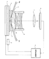
図1は本発明による顕微鏡を有する検査装置の全体構成を示す図である。図2は、図1に示す検査装置の照明ビーム投射部の構成を示す平面図であり、図3は光源装置の一例を示す図である。本発明では、試料表面に対して暗視野照明を行い、試料の内部からの散乱光を検出することにより欠陥検出を行う。検査されるべき試料(半導体基体)1はステージ2上に載置する。本例では、欠陥検査されるべき試料として、半導体基板上に各種半導体層や多層膜構造体が形成されている半導体基体を用い、半導体層や多層膜構造体の内部に存在する欠陥や多層膜構造体に形成された孔や溝に存在する欠陥或いは半導体層の内部に形成された配線パターンに存在する欠陥等の各種欠陥を検出する。半導体基体として、例えばシリコン基板上に酸化シリコン膜とシリコン材料層とが積層された多層膜構造体が用いられる。 FIG. 1 is a view showing the overall configuration of an inspection apparatus having a microscope according to the present invention. FIG. 2 is a plan view showing the configuration of the illumination beam projection unit of the inspection apparatus shown in FIG. 1, and FIG. 3 is a view showing an example of the light source device. In the present invention, dark field illumination is performed on the sample surface, and defect detection is performed by detecting scattered light from the inside of the sample. The sample (semiconductor substrate) 1 to be inspected is placed on the stage 2. In this example, a semiconductor substrate in which various semiconductor layers and multilayer film structures are formed on a semiconductor substrate is used as a sample to be inspected for defects, and defects and multilayer films existing inside the semiconductor layer and multilayer film structure. Various defects such as defects present in holes or trenches formed in the structure or defects present in a wiring pattern formed inside the semiconductor layer are detected. As a semiconductor substrate, for example, a multilayer film structure in which a silicon oxide film and a silicon material layer are stacked on a silicon substrate is used.
ステージ2として、第1の方向(X方向)及び第1の方向と直交する第2の方向(Y方向)に移動可能なXYステージが用いられ、試料を支持すると共に走査系を構成する。ステージ2は、信号処理装置3から供給される駆動信号によりX方向及びY方向にジッグザグ状に移動し、検査される半導体基体1は照明ビームによりその全面が走査される。ステージ2には位置センサ4が連結され、移動中のステージのX方向及びY方向の位置が検出され、位置情報として信号処理装置3に供給される。信号処理装置3は、入力した位置情報を用いて検出された欠陥のアドレスを特定する。 As the stage 2, an XY stage movable in a first direction (X direction) and a second direction (Y direction) orthogonal to the first direction is used to support a sample and configure a scanning system. The stage 2 moves in a zigzag manner in the X and Y directions in response to a drive signal supplied from the signal processing device 3, and the entire surface of the semiconductor substrate 1 to be inspected is scanned by the illumination beam. A position sensor 4 is connected to the stage 2 to detect the position of the moving stage in the X and Y directions, and is supplied to the signal processing device 3 as position information. The signal processing device 3 specifies the address of the detected defect using the input position information.
照明ビーム投射部5から、ステージ上に載置された半導体基体1に向けて光学的に透明な波長域の照明ビームを投射する。図1においては、照明ビームを投射する2本の偏波面保存ファイバだけを図示する。これら偏波面保存ファイバから照明ビームが投射され、半導体基体1に照明エリアを形成する。尚、偏波面保存ファイバは、半導体基体に対してP偏光した照明光をブリュースター角にほぼ等しい入射角で投射する。従って、後述するように、半導体基体1の表面における反射率はほぼ零となり、投射された照明光の大部分は半導体基体の内部に進入する。半導体基体の内部に欠陥が存在すると、欠陥部分から散乱光が発生する。発生した散乱光は、半導体基体から出射し、対物レンズ6により集光される。尚、偏波面保存ファイバは、先端側において被覆を取り除き、クラッドが露出した状態にする。
An illumination beam of an optically transparent wavelength range is projected from the illumination
対物レンズ6により集光された散乱光は、結像レンズ7を経て光検出手段8に入射する。本例では、光検出手段としてTDIセンサを用いる。TDIセンサの電荷転送速度は走査系を構成するステージ2の主走査速度と対応させる。TDIセンサ8から出力される画像信号は信号処理装置3に供給される。尚、光検出手段として、2次元CCDセンサを用いることもできる。
The scattered light collected by the
信号処理装置3は、半導体基体から出射する散乱光による暗視野画像を形成する。そして、形成された画像を用いてダイ対ダイ比較検査により又はダイ対データベース比較検査により欠陥を検出すると共に検出された欠陥のアドレスを特定する。すなわち、半導体基体の内部に欠陥が存在すると、例えば半導体層や多層膜構造体中に形成された孔や溝の内部に異物が存在する場合、当該異物に照明光が入射すると、異物から散乱光が発生する。発生した散乱光は対物レンズにより集光されるため、暗視野画像をダイ対ダイ比較検査を行うことにより欠陥として検出される。また、コンタクトホールのような電極が形成される孔の底面及びトレンチの底面には、エッチングにより微細な凹凸が形成され、当該孔又はトレンチの底面に照明光が入射した場合、孔の底面から散乱光が発生する。この場合、エッチング不良により所定の深さの孔やトレンチが形成されていない場合、本来形成されるべき底面の散乱光画像の位置からずれた位置に散乱光画像が形成されるため、暗視野画像に基づくダイ対ダイ比較検査又はダイ対データベースの比較検査によりエッチング不良の孔を検出することが可能である。さらに、TSV技術を利用した半導体デバイスの製造工程においても、エッチング不良により半導体基体に正確なTSVが形成されていない場合、散乱光検出により欠陥として検出することが可能である。尚、半導体層の欠陥以外の正常な部分から散乱光が発生する場合もあるが、ダイ対ダイ等の比較検査を行えば、正常な部分からの散乱光はキャンセルされるため、欠陥からの散乱光成分だけを抽出することができる。 The signal processing device 3 forms a dark field image by scattered light emitted from the semiconductor substrate. Then, the formed image is used to detect a defect by die-to-die comparison inspection or die-to-database comparison inspection and identify the address of the detected defect. That is, if a defect is present inside the semiconductor substrate, for example, if foreign matter is present inside the hole or groove formed in the semiconductor layer or the multilayer film structure, scattered light from the foreign matter when illumination light is incident on the foreign matter Occurs. Since the generated scattered light is collected by the objective lens, the dark field image is detected as a defect by performing die-to-die comparison inspection. In addition, minute unevenness is formed by etching on the bottom of the hole and the bottom of the trench where the electrode such as the contact hole is formed, and when the illumination light is incident on the bottom of the hole or the trench, scattering from the bottom of the hole Light is generated. In this case, when a hole or a trench having a predetermined depth is not formed due to an etching failure, a scattered light image is formed at a position deviated from the position of the scattered light image on the bottom surface to be originally formed. It is possible to detect holes with etch defects by die-to-die comparison inspection based on or die-to-database comparison inspection. Furthermore, also in the process of manufacturing a semiconductor device using the TSV technology, when an accurate TSV is not formed on the semiconductor substrate due to etching failure, it is possible to detect as a defect by scattered light detection. Although scattered light may be generated from normal parts other than defects in the semiconductor layer, scattered light from normal parts will be canceled if comparative inspection of die to die etc. is performed, so scattering from defects may occur. Only light components can be extracted.
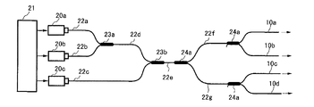
次に、照明ビームの投射方法について説明する。図2は、対物レンズの光軸方向にそって照明ビーム投射部5を見た平面図である。図1及び図2を参照して、照明ビーム投射部5について説明する。照明ビーム投射部は、半導体基体1の表面に向けて照明ビームを投射する4本の偏波面保存ファイバ10a〜10dと、これら偏波面保存ファイバを支持する支持プレート11と、偏波面保存ファイバ10a〜10dを支持プレート11に固定するための押えプレート12とを有する。4本の偏波面保存ファイバ10a〜10dは、それらの先端側は被覆が取り除かれた状態に維持する。そして、支持プレート11には、照明エリアを中心にして円環状に等間隔で4つのV溝が形成され、これらV溝中に4本の偏波面保存ファイバを配置し、接着剤により固定する。さらに、各V溝中に偏波面保存ファイバをそれぞれ配置した状態で押えプレート12を接着剤により取付け、4本の偏波面保存ファイバを固定する。尚、本例では、4本の偏波面保存ファイバを用いる例について説明したが、1本の偏波面保存ファイバを用いる場合であっても、本発明を適用することができる。
Next, the projection method of the illumination beam will be described. FIG. 2 is a plan view of the illumination
支持プレート11に形成された各V溝は、試料表面に対して試料のブリュースター角にほぼ等しい入射角で照明ビームが入射するように傾斜を設ける。例えば、シリコン基板に形成された半導体層や多層膜構造体の内部を検査する場合、近赤外域の波長光を用いた場合シリコン材料のブリュースター角は約75°であるため、各偏波面保存ファイバ10a〜10dの光出射端から出射する照明ビームが半導体基体1の表面に対して約75°の入射角で入射するように偏波面保存ファイバを支持する。尚、試料の光学特性に応じてブリュースター角が相違するため、検査すべき試料の光学特性に応じて対応するブリュースター角に等しい入射角で照明できるように、傾斜角度が設定された支持プレートを用意することが望ましい。尚、照明ビームは、試料に対してブリュースター角に厳格に一致させることが望ましいが、ブリュースター角から僅かに変位した入射角であっても、同様な効果が得られるので、ブリュースター角から僅かな角度だけずれた場合であってもよい。
Each V-groove formed in the support plate 11 is inclined so that the illumination beam is incident on the sample surface at an incident angle substantially equal to the Brewster's angle of the sample. For example, when inspecting the inside of a semiconductor layer or multilayer film structure formed on a silicon substrate, when using wavelength light in the near infrared region, the Brewster's angle of the silicon material is approximately 75 °. The polarization maintaining fiber is supported such that the illumination beam emitted from the light emitting ends of the
さらに、本例では、照明ビーム投射用の4本の偏波面保存ファイバは、試料表面に設定された照明エリアを中心にして円環状に等角度で配置する。これにより、試料を異なる複数の角度方向から照明することができる。 Furthermore, in the present example, the four polarization-maintaining fibers for projecting the illumination beam are arranged at an equal angle in an annular shape centering on the illumination area set on the sample surface. Thereby, the sample can be illuminated from a plurality of different angular directions.
本発明では、光源装置から直線偏光した照明光を放出し、偏波面保存ファイバを介して半導体基体の表面に向けてP偏光した照明光として投射する。このため、光源装置から出射した照明光がP偏光した照明光として半導体基体1の表面に入射するように偏波面保存ファイバ10a〜10dを設定する。すなわち、各偏波面保存ファイバは、光源装置から放出された直線偏光した照明光の電気ベクトルの振動方向が入射面に平行になるように設定する。
In the present invention, linearly polarized illumination light is emitted from the light source device, and is projected as P-polarized illumination light toward the surface of the semiconductor substrate through the polarization-maintaining fiber. Therefore, the polarization
次に、光源装置について説明する。本例では、光源装置として、それぞれ波長の異なる照明光を発生する3個のスーパールミネッセント発光ダイオード(SLED)20a〜20cを用い、検査すべき試料の光学特性に応じて最適な波長域の照明光を発生する。例えば、半導体多層膜が形成された半導体基体について検査を行う場合、半導体多数膜は干渉層として作用する場合があり、半導体層間の界面で反射する成分が多くなり、内部に進入する照明光量が低下する場合がある。このような場合、半導体層の膜厚や屈折率等の光学特性に応じて照明光の波長を適切に選択することにより、多層膜中に進入する照明光の光量を増大させることができる。 Next, the light source device will be described. In this example, three super luminescent light emitting diodes (SLEDs) 20a to 20c that respectively generate illumination light of different wavelengths are used as light source devices, and an optimal wavelength range is selected according to the optical characteristics of the sample to be inspected. Generate illumination light. For example, when inspecting a semiconductor substrate on which a semiconductor multilayer film is formed, the semiconductor multiple film may act as an interference layer, and the component reflected at the interface between the semiconductor layers increases, and the amount of illumination light entering the interior decreases. May. In such a case, by appropriately selecting the wavelength of the illumination light in accordance with the optical characteristics such as the film thickness and the refractive index of the semiconductor layer, the light amount of the illumination light entering the multilayer film can be increased.
本例では、第1のSLED20aは中心周波数λ1が、λ1=680nmの照明光を発生し、第2のSLED20bは中心周波数λ2が、λ2=1310nmの照明光を発生し、第3のSLED20cはλ3=1550nmの照明光を発生する。これら第1〜第3のSLED20a〜20cは、制御回路21に接続され、各SLED素子に供給される駆動電流を切り換えることにより選択的に点灯及び消灯することができる。尚、上述した照明光の波長は一例であり、検査される試料の特性に応じて最適な波長の照明光を発生するSLEDを用いることができる。
In this example, the
SLEDの特性として、直線偏光した光ビームを発生すると共に点光源として作用する。従って、点光源として作用する特性を利用することにより、SLEDに単一モード光ファイバを結合した場合、SLEDから出射した光ビームをほぼ損失させることなく単一モード光ファイバを伝搬させて任意の位置から照明光を放出することが可能である。これに対して、通常の発光ダイオード(LED)は面発光素子であるため、単一モード光ファイバに接続した場合、損失が大きすぎる欠点がある。さらに、SLEDの特性として、直線偏光した光ビームを発生するため、SLEDに偏波面保存ファイバを結合すれば、検査すべき試料表面まで偏光状態が保存された状態で伝搬させることが可能である。よって、照明ビームを投射する偏波面保存ファイバを適切に設定することにより、試料表面に対して所望の偏光状態の照明光として投射することができ、試料表面に対してP偏光した照明光として投射することが可能である。後述するように、P偏光した照明光を試料表面に対してブリュースター角に等しい入射角で照明する場合、反射率は零になるため、表面反射がほぼ零となり、フレアが大幅に低減された照明システムを構築することが可能になると共に照明光の利用効率が格段に改善された照明システムが構築される。さらに、SLEDの利点として、比較的ブロードなスペクトル特性を有し時間的にインコヒーレントな光ビームを放出するため、スペックルパターンのない照明ビームを放出できる利点がある。上述したSLEDの利点を考慮し、本例では、照明光源としてSLED(スーパールミネッセント発光ダイオード)を用いる。 As a characteristic of SLED, it generates a linearly polarized light beam and acts as a point light source. Therefore, by utilizing the property of acting as a point light source, when a single mode optical fiber is coupled to the SLED, the single mode optical fiber can be propagated to any position without substantially losing the light beam emitted from the SLED. It is possible to emit illumination light from On the other hand, since a normal light emitting diode (LED) is a surface light emitting element, there is a drawback that the loss is too large when connected to a single mode optical fiber. Furthermore, since a linearly polarized light beam is generated as a characteristic of the SLED, if a polarization maintaining fiber is coupled to the SLED, it is possible to propagate the state of polarization to the surface of the sample to be inspected. Therefore, by appropriately setting the polarization maintaining fiber for projecting the illumination beam, it can be projected as illumination light of a desired polarization state on the sample surface, and it is projected as illumination light P-polarized on the sample surface It is possible. As described later, when the P-polarized illumination light is illuminated at an incident angle equal to Brewster's angle with respect to the sample surface, the reflectance is zero, so the surface reflection is almost zero, and flare is significantly reduced. A lighting system can be constructed, and the utilization efficiency of the illumination light is remarkably improved. Furthermore, an advantage of SLEDs is that they emit relatively incoherent light beams with relatively broad spectral properties, so that they can emit illumination beams without speckle patterns. In view of the advantages of the SLEDs described above, in this example, SLEDs (super luminescent light emitting diodes) are used as illumination light sources.
第1〜第3のSLED20a〜20cには、第1〜第3の偏波面保存ファイバ22a〜22cをそれぞれ接続する。第1の偏波面保存ファイバ22aと第2の偏波面保存ファイバ22bは第1のWDMカプラ(Wavelength Division Multiplexingカプラ)23aに接続され、その出射端は第4の偏波面保存ファイバ22dに接続する。第4の偏波面保存ファイバ22dと第3の偏波面保存ファイバ22cは第2のWDMカプラ23bに接続され、その出射端は第5の偏波面保存ファイバ22eに接続する。第5の偏波面保存ファイバの出射端は、第1の3dBカプラ24aに接続する。第1の3dBカプラの出射端には第6及び第7の偏波面保存ファイバ22f及び22gを接続する。第6の偏波面保存ファイバには、第2の3dBカプラ24bを介して第1及び第2の照明ビーム投射用の偏波面保存ファイバ10a及び10bを結合する。第7の偏波面保存ファイバ22gには、第3の3dBカプラ24cを介して第3及び第4の照明ビーム投射用の偏波面保存ファイバ10c及び10dを結合する。
The first to third
制御回路21の制御のもとで、第1〜第3のSLED20a〜20cのいずれかに駆動電流を供給して照明光を発生させると、SLEDから出射した照明光は、全ての照明ビーム投射用の偏波面保存ファイバ10a〜10dに均一に入射し、これら偏波面保存ファイバから偏光状態が保存された状態で均一の光量の照明ビームがそれぞれ出射する。このように、試料の特性に応じて照明光の波長を選択できるため、試料ごとに最適な波長の照明光により照明することが可能である。例えば、検査されるべき半導体基体が半導体多層膜構造の場合、半導体層の膜厚や屈折率等の特性を考慮して、試料ごとに最適な照明条件を設定することができる。尚、上述した構成の照明系を複数個設け、多数の角度方向から照明ビームを投射することも可能である。
Under the control of the
図3に示す構造の光源装置の変形例として、以下の態様の光源装置を用いることができる。検査に際し、3個のSLED20a〜20cを同時に点灯する。この場合、各SLEDから出射した波長の異なる光ビームは、4本の偏波面保存ファイバ10a〜10dに均一の光量の光ビームとしてそれぞれ入射するので、試料表面は波長の異なる3本の光ビームにより同時に走査される。この場合、例えば多層膜構造体の内部に、膜厚や屈折率等との関係より、特定の波長域の光に対して反射率が高い部分や屈折率が大きい部分が局所的に存在する場合であっても、波長の異なる複数の検査光により同時走査されるので、欠陥から散乱光を発生させ、発生した散乱光を検出することが可能になる。
The light source device of the following aspect can be used as a modification of the light source device of the structure shown in FIG. At the time of inspection, three
さらに、第1〜第3のSLED20a〜20cとして同一波長の光ビームを発生するSLEDを用い、検査に際して3個のSLEDを同時に点灯することができる。この場合、3個のSLEDから出射した光ビームは、4つの偏波面保存ファイバ10a〜10dに均一に入射するので、1個のSLEDだけを点灯した場合と比較して各偏波面保存ファイバから3倍の光量の照明ビームがそれぞれ出射する。よって、1個のSLEDだけでは十分な照明光量が得られない場合に有益である。
Furthermore, SLEDs that generate light beams of the same wavelength can be used as the first to
上述した実施例では、光源装置として3個のSLEDを用いたが、1個のSLEDを用いる場合であってもよい。また、1個のSLEDと1本の偏波面保存ファイバとを組合せた実施例の場合、偏波面保存ファイバをSLEDに直接光学的に接続することができる。 Although three SLEDs are used as the light source device in the embodiment described above, one SLED may be used. Also, in the embodiment where one SLED and one polarization maintaining fiber are combined, the polarization maintaining fiber can be directly optically connected to the SLED.
本発明による顕微鏡及び検査装置は、主として半導体基体の内部に存在する欠陥を検出することを目的とするため、照明光の表面反射をできるだけ低減する必要がある。そこで、本発明では、各照明ビームは、試料表面に対してブリュースター角にほぼ等しい入射角で投射する。図4は、シリコン基板における入射角と反射率との関係を示すグラフである。図4において、横軸は入射角を示し、縦軸は反射率を示す。また、破線はS偏光した光ビームの特性を示し、実線はP偏光した光ビームの特性を示す。入射する光ビームがP偏光の場合、入射角がブリュースター角に等しい場合、反射率は零であり、光ビームはシリコン基板を透過する。シリコン基板の近赤外域におけるブリュースター角はほぼ75°である。従って、照明ビームをブリュースター角に等しい入射角で半導体基体の表面に向けて投射すれば、表面反射がほぼ零の照明光学系が構築される。 Since the microscope and inspection apparatus according to the present invention are mainly intended to detect defects present inside the semiconductor substrate, it is necessary to reduce the surface reflection of the illumination light as much as possible. Thus, in the present invention, each illumination beam is projected onto the sample surface at an angle of incidence approximately equal to the Brewster angle. FIG. 4 is a graph showing the relationship between the incident angle and the reflectance in a silicon substrate. In FIG. 4, the horizontal axis indicates the incident angle, and the vertical axis indicates the reflectance. The broken line indicates the characteristics of the S-polarized light beam, and the solid line indicates the characteristics of the P-polarized light beam. If the incident light beam is P-polarized, and the incident angle is equal to Brewster's angle, the reflectivity is zero and the light beam passes through the silicon substrate. The Brewster angle in the near infrared region of the silicon substrate is approximately 75 °. Thus, by projecting the illumination beam towards the surface of the semiconductor substrate at an angle of incidence equal to the Brewster's angle, an illumination optical system with almost zero surface reflection is constructed.
さらに重要なことは、偏波面保存ファイバを用いてブリュースター角に等しい入射角で照明する場合、対物レンズと試料との間の空間に照明ビーム投射部を配置することができるので、対物レンズに対する空間的な制約が大幅に減少し、開口数の大きな対物レンズを用いることが可能になる。特に、シリコン材料のブリュースター角は75°であり、且つ偏波面保存ファイバの先端部分の直径は125μm程度であるから、開口数の大きな対物レンズを使用することが可能になり、高分解能の欠陥検査を行うことができる。 More importantly, when the polarization maintaining fiber is used to illuminate at an angle of incidence equal to Brewster's angle, the illumination beam projection unit can be arranged in the space between the objective lens and the sample, Spatial constraints are greatly reduced, and it is possible to use a large numerical aperture objective. In particular, since the Brewster angle of the silicon material is 75 ° and the diameter of the tip portion of the polarization maintaining fiber is about 125 μm, it becomes possible to use an objective lens with a large numerical aperture, and a defect of high resolution The examination can be done.
図5は試料と照明光との関係を示す図である。本例では、検査される試料として、シリコン基板上に各種シリコン材料層と酸化シリコン層との多層膜構造体が形成されている半導体基体について説明する。図5(A)は、シリコン材料層が形成されている表面側から照明光を投射して欠陥検出を行う例を示し、図5(B)は半導体基板の裏面側から照明光を投射して表面側に形成されている多層膜構造体に存在する欠陥を検出する例を示す。図5(A)を参照するに、シリコン基板30上にシリコン材料層31が形成され、シリコン材料層31中にコンタクホール32a〜32dが形成されている。そして、検査の後にコンタクトホールに柱状電極が形成されるものとする。尚、シリコン材料層は、例えば単結晶又は多結晶シリコン層と酸化シリコン層とが形成された多層膜構造とする。今、コンタクトホール32bの側壁に異物付着による欠陥が33が存在するものとする。波長が近赤外域のP偏光した照明ビームがシリコン材料層31の表面にブリュースター角に等しい入射角で入射すると、表面反射率が零のため、ほとんどの照明光がシリコン材料層の内部に進入する。欠陥のない部分では、照明光はシリコン材料層31及び半導体基板30を透過し、外部に出射する。一方、シリコン材料層の内部に進入した照明ビームがコンタクトホール32bの側壁に入射すると、異物33から散乱光が発生し、発生した散乱光の一部はシリコン材料層を透過し、対物レンズにより集光される。よって、対物レンズにより集光された散乱光を光検出手段により検出することにより、欠陥が検出される。尚、シリコン材料層とシリコン基板との間の界面や他の界面等で反射した反射光は、シリコン材料層の表面からほぼ75°の角度で出射するため、対物レンズの集光範囲から外れ、対物レンズにより集光されない。
FIG. 5 is a view showing the relationship between the sample and the illumination light. In this example, a semiconductor substrate having a multilayer film structure of various silicon material layers and a silicon oxide layer formed on a silicon substrate will be described as a sample to be inspected. FIG. 5A shows an example in which illumination light is projected from the surface side where the silicon material layer is formed to perform defect detection, and FIG. 5B is a projection of illumination light from the back surface side of the semiconductor substrate. The example which detects the defect which exists in the multilayer film structure currently formed in the surface side is shown. Referring to FIG. 5A, a
図5(B)に示すように、本発明では、シリコン基板の裏面30bから照明ビームを投射することもできる。すなわち、中心波長が近赤外域のP偏光した照明光をブリュースター角に等しい入射角で投射すれば、ほとんどの照明光がシリコン基板30の表面で反射せず、基板の内部に進入する。基板の内部に進入した照明光は、シリコン基板30の表面側に形成されたシリコン材料層31及びシリコン材料層に形成されたコンタクトホール32a〜32dの底面及びその側壁を照明する。この場合、コンタクトホール32cの底面に異物付着に起因する欠陥34が存在する場合、コンタクトホールの底面から散乱光が発生する。発生した散乱光は、シリコン材料層31及びシリコン基板30を透過するので、シリコン基板30の裏面30bから出射し、対物レンズにより集光される。従って、シリコン基板の裏面側から照明光を投射しても、シリコン材料層に存在する欠陥を検出することが可能である。
As shown in FIG. 5B, in the present invention, the illumination beam can also be projected from the back surface 30b of the silicon substrate. That is, when P-polarized illumination light having a central wavelength in the near infrared range is projected at an incident angle equal to Brewster's angle, most of the illumination light does not reflect on the surface of the
このシリコン基板の裏面側から照明する方法は、CMOSセンサ等のデバイスの製造工程における欠陥検査において有益である。すなわち、CMOSセンサやCCDセンサの製造プロセスにおいては、基板の表面側に素子形成領域が形成された後、シリコン基板の裏面側を研磨する裏面研磨が行われる。よって、裏面研磨後に基板の裏面側から照明光を投射して表面側に形成された半導体層に形成された欠陥を検出することは、製造の歩留りを改善する上で有効である。 This method of illuminating from the back side of the silicon substrate is useful in defect inspection in the manufacturing process of devices such as CMOS sensors. That is, in the manufacturing process of the CMOS sensor or the CCD sensor, after the element forming region is formed on the front surface side of the substrate, the back surface polishing for polishing the back surface side of the silicon substrate is performed. Therefore, it is effective to improve the manufacturing yield by projecting illumination light from the back surface side of the substrate after polishing the back surface and detecting a defect formed in the semiconductor layer formed on the front surface side.
本例では、コンタクトホールに形成された欠陥を検出する例について説明したが、勿論シリコン材料層の内部に存在する各種欠陥を検出することができる。 In this example, although the example which detects the defect formed in the contact hole was demonstrated, of course, the various defects which exist inside a silicon material layer can be detected.
次に、偏波面保存ファイバから出射する照明ビームの拡がり防止について説明する。図6(A)は、偏波面保存ファイバ40から出射した照明ビームが半導体基体41の表面に入射する際、半導体基体の表面に発散した状態で入射する態様を示す。偏波面保存ファイバから出射する照明ビームは発散性ビームであるため、試料表面上において入射面内の光軸と直交する方向及び入射面と直交する方向に拡がった照明エリアが形成される。ここで、入射面とは、照明ビームの光軸を含み試料表面と直交する面を示すものとする。照明ビームが発散性ビームであるため、偏波面保存ファイバを試料表面に対してブリュースター角に設定しても、照明ビームの中心から半径方向に変位した周辺のビーム部分は拡がり角が大きいため、ブリュースター角から外れた角度で試料表面に入射する。この結果、照明エリアの中心から変位した周辺部において、試料表面を透過し内部に伝搬する照明ビームの光量が低下する不具合がある。また、照明エリアの輝度分布も中心から周辺に変位するにしたがって輝度が低下する不具合が発生する。
Next, prevention of the spread of the illumination beam emitted from the polarization maintaining fiber will be described. FIG. 6A shows a mode in which the illumination beam emitted from the
上記課題を解決するため、本発明では、偏波面保存ファイバ40の先端に、照明ビームの拡がり角を抑制する光学素子を固定する。この光学素子として、図6(B)に示すように、例えば屈折率分布型レンズ(GRINレンズ)42を用いることができる。屈折率分布型レンズ42は、光ファイバと同様な直径のロッド状のレンズ素子であり、屈折率が中心から半径方向外側に向けて徐々に大きくなるように分布した形態を有する。本例では、屈折率分布型レンズとして、コリメータレンズとして作用する光学素子42を用いる。このような光学素子は、アーク放電により偏波面保存ファイバの先端に融着することができる。よって、偏波面保存ファイバの先端にコリメータレンズとして作用する光学素子42を固定することにより、図6(D)に示すように、照明ビーム全体が照明ビームの光軸に平行なビームとして出射する。また、別の光学素子として、図6(C)に示すように、ロッド状の透明体の先端を球面43aに形成したロッド状レンズ43を用いることもできる。
In order to solve the above problems, in the present invention, an optical element for suppressing the spread angle of the illumination beam is fixed to the tip of the
ビームの拡がり角抑制手段の変形例として、一方向にだけ集束性を有するシリンドリカルレンズを用いて円形の照明エリアを形成することができる。偏波面保存ファイバをブリュースター角に等しい角に設定した場合、光軸と直交する入射面内方向のビームの拡がり量は、入射面と直交する方向の拡がり量よりも大きいため、試料表面上に形成される照明エリアが楕円形となり、光量分布が形成されてしまう。そこで、照明ビームの拡がり角を抑制する光学素子としてシリンドリカルレンズを用い、ほぼ円形の照明エリアを形成する。屈折率分布型レンズにおいて、一方向にのみ中心から半径方向に屈折率が徐々に増大する屈折率分布を有する場合、一方向にだけ集束性を有するロッド状のシリンドリカルレンズが形成される。 As a modification of the beam spread angle suppressing means, a circular illumination area can be formed by using a cylindrical lens having a focusing property in only one direction. When the polarization maintaining fiber is set to an angle equal to the Brewster's angle, the beam spread in the in-plane direction orthogonal to the optical axis is larger than the spread in the direction orthogonal to the incident plane. The illumination area to be formed becomes elliptical, and the light quantity distribution is formed. Therefore, a cylindrical lens is used as an optical element for suppressing the spread angle of the illumination beam to form a substantially circular illumination area. In the gradient index lens, in the case of having a refractive index distribution in which the refractive index gradually increases in the radial direction from the center only in one direction, a rod-shaped cylindrical lens having a focusing property in only one direction is formed.
図7において、(A)は先端にシリンドリカルレンズ44が融着された偏波面保存ファイバ40を上方から見た線図的平面図であり、(B)は側方から見た側面図である。偏波面保存ファイバ40の先端にロッド状のシリンドリカルレンズ44を融着し、シリンドリカルレンズの集束度を入射面内における光軸と直交する方向のビーム拡がり角が偏波面保存ファイバのビーム拡がり角と等しくなるように設定すれば、試料表面上にほぼ円形の照明エリア45を形成することできる。
In FIG. 7, (A) is a schematic plan view of the polarization-maintaining
図8は信号処理装置の欠陥検出部の構成を示す図である。TDIセンサ8から出力される画像信号は増幅された後2次元画像形成手段50に供給される。2次元画像形成手段は、入力した画像信号から試料の2次元画像を形成する。本例では、ダイ対ダイ比較検査により欠陥を検出する。よって、2次元画像形成手段は、1つのダイの2次元画像を形成し、画像メモリ51に供給する。1つのダイについての検査が終了した後、隣接するダイについて検査が行われ、隣接するダイの2次元画像情報が2次元画像形成手段50から画像メモリ51に供給されると共に画像比較手段52にも供給される。画像比較手段52には、直前のダイの2次元画像が同期して画像メモリ51から画像比較手段52に供給される。
FIG. 8 is a diagram showing the configuration of a defect detection unit of the signal processing apparatus. The image signal output from the TDI sensor 8 is amplified and then supplied to the two-dimensional
画像比較手段52には、1つ前に検査されたダイの画像信号と検査中のダイの画像信号とが同期して入力する。画像比較手段52は、入力した2つの画像信号から輝度比較を行う。そして、輝度差が所定の閾値を超える場合欠陥と判定し、その判定結果を欠陥メモリ53に供給する。ステージの位置を検出する位置センサ4からの出力信号も欠陥メモリ53に供給される。そして、欠陥メモリ53には、画像比較手段52から出力された欠陥判定信号が入力した際のアドレスを欠陥のアドレスとして記憶する。
The image comparison means 52 synchronously inputs the image signal of the die inspected immediately before and the image signal of the die under inspection. The image comparison means 52 performs luminance comparison from the two input image signals. Then, when the luminance difference exceeds a predetermined threshold value, it is determined as a defect, and the determination result is supplied to the
次に、対物レンズにより集光される散乱光の散乱角について説明する。図9(A)は落射照明において対物レンズにより集光される散乱光の散乱角の範囲を示し、図9(B)は本発明の顕微鏡において対物レンズにより集光される散乱光の散乱角の範囲を示す。図9において、図1で用いた構成要素と同一の構成要素には同一符号を付して説明する。また、対物レンズの集光角をθとし、本発明の照明ビームの入射角をαとする。落射照明の場合、照明ビームは試料表面に対して垂直に入射するので、対物レンズにより集光される散乱光の散乱角の範囲は、0°〜θとなる。これに対して、本発明の照明光学系において、対物レンズにより集光される散乱光の散乱角の範囲は、α−θ〜α+θとなる。すなわち、落射照明の場合、散乱角の小さい散乱光が対物レンズにより集光され、散乱角の比較的大きな散乱光は検出されない。これに対して、本発明のように、軸外照明の場合散乱角の大きな散乱光が対物レンズにより集光され、比較的小さい散乱角の散乱光は集光されない特性がある。 Next, the scattering angle of the scattered light collected by the objective lens will be described. FIG. 9A shows the range of the scattering angle of scattered light collected by the objective lens in incident illumination, and FIG. 9B shows the scattering angle of scattered light collected by the objective lens in the microscope of the present invention Indicate the range. In FIG. 9, the same components as the components used in FIG. 1 will be described with the same reference numerals. Also, let the collection angle of the objective lens be θ, and let the incidence angle of the illumination beam of the present invention be α. In the case of epi-illumination, since the illumination beam is perpendicularly incident on the sample surface, the range of the scattering angle of the scattered light collected by the objective lens is 0 ° to θ. On the other hand, in the illumination optical system of the present invention, the range of the scattering angle of the scattered light collected by the objective lens is α-θ to α + θ. That is, in the case of epi-illumination, scattered light with a small scattering angle is collected by the objective lens, and scattered light with a relatively large scattering angle is not detected. On the other hand, as in the present invention, in the case of off-axis illumination, scattered light with a large scattering angle is collected by the objective lens, and scattered light with a relatively small scattering angle is not collected.
次に、欠陥のサイズと散乱角との関係について検討する。一般的に、サイズの大きな欠陥から出射する散乱光の散乱角は小さく、サイズの小さい欠陥から出射する散乱光の散乱角は相対的に大きいことが知られている。この技術的認識に立てば、本発明のように、軸外照明を行う顕微鏡においては、散乱角の大きな散乱光が検出されるので、より微細な欠陥を検出できる利点が達成される。 Next, the relationship between the size of the defect and the scattering angle is examined. Generally, it is known that the scattering angle of scattered light emitted from a large defect is small, and the scattering angle of scattered light emitted from a small defect is relatively large. In this technical recognition, in the microscope performing off-axis illumination as in the present invention, since scattered light with a large scattering angle is detected, the advantage of being able to detect finer defects is achieved.
本発明は上述した実施例だけに限定されず、種々の変更や変形が可能である。例えば、上述した実施例では、4本の照明ビーム投射用の偏波面保存ファイバを用いて4方向から照明したが、多数の照明ビーム投射用の偏波面保存ファイバを用いて多数の角度方向から試料を照明することが可能である。また、1本の偏波面保存ファイバを光源装置に直接接続して一方向からP偏光した照明ビームを投射することもできる。
さらに、SLEDの中心波長は例示したものであり、試料の光学特性に応じて中心波長の異なる複数のSLEDを用いることもできる。
The present invention is not limited to the embodiments described above, and various modifications and variations are possible. For example, in the above-described embodiment, illumination is performed from four directions using polarization maintaining fibers for projecting four illumination beams, but samples using polarization maintaining fibers for projecting a large number of illumination beams are used from a large number of angular directions. It is possible to illuminate the Also, it is possible to directly connect one polarization maintaining fiber to the light source device to project a P-polarized illumination beam from one direction.
Furthermore, the center wavelength of SLED is illustrated, and it is also possible to use a plurality of SLEDs having different center wavelengths according to the optical characteristics of the sample.
上述した実施例では、シリコン基板上に多層膜構造体が形成された半導体基体に存在する欠陥を検出する検査装置を一例として説明したが、シリコン基板以外の各種材料基板、例えば炭化珪素基板上に炭化珪素の材料膜が形成されている試料の表面及び内部に存在する欠陥を検出する検査装置にも適用することができる。 In the embodiment described above, an inspection apparatus for detecting a defect present in a semiconductor substrate having a multilayer film structure formed on a silicon substrate has been described as an example, but various material substrates other than silicon substrates, for example, silicon carbide substrates The present invention can also be applied to an inspection apparatus that detects defects present on the surface and in the inside of a sample on which a silicon carbide material film is formed.
1 半導体基体
2 ステージ
3 信号処理装置
4 位置センサ
5 照明ビーム投射部
6 対物レンズ
7 結像レンズ
8 光検出手段
10a〜10d 照明ビーム投射用の偏波面保存ファイバ
11 支持プレート
12 押えプレート
20a〜20c SLED
21 制御回路
22a〜22g 偏波面保存ファイバ
23a,23b WDMファイバカプラ
24a〜24c 3dBカプラ
30 シリコン基板
31 シリコン材料層
32 コンタクトホール
33,34 欠陥
Reference Signs List 1 semiconductor substrate 2 stage 3 signal processing device 4
11
21 Control circuit
22a to 22g
24a to 24c 3
Claims (23)
光源装置に光学的に結合され、光源装置から出射し直線偏光した光ビームを試料表面の照明エリアにP偏光した照明ビームとして投射する偏波面保存ファイバと、
光軸が前記試料表面に対して直交するように配置され、試料から発生した散乱光を集光する対物レンズと、
対物レンズにより集光された散乱光を受光する光検出手段とを有し、
前記偏波面保存ファイバは、試料表面に対してブリュースター角にほぼ等しい入射角でP偏光した照明ビームを投射することを特徴とする顕微鏡。 A light source device for generating a linearly polarized light beam;
A polarization maintaining fiber which is optically coupled to the light source device and projects the linearly polarized light beam emitted from the light source device onto the illumination area of the sample surface as a P-polarized illumination beam;
An objective lens disposed so that the optical axis is orthogonal to the surface of the sample and collecting scattered light generated from the sample;
And light detection means for receiving scattered light collected by the objective lens,
A microscope characterized in that the polarization maintaining fiber projects a P-polarized illumination beam at an incident angle substantially equal to Brewster's angle to a sample surface.
光源装置に光学的に結合され、光源装置から出射し直線偏光した照明光を、試料表面の照明エリアにP偏光した照明光として投射する複数本の偏波面保存ファイバと、
光軸が前記試料表面に対して直交するように配置され、試料から発生した散乱光を集光する対物レンズと、
対物レンズにより集光された散乱光を受光する光検出手段とを有し、
前記偏波面保存ファイバは、試料表面に対してブリュースター角にほぼ等しい入射角でP偏光した照明ビームを投射し、
前記複数本の偏波面保存ファイバの光出射端は試料表面の照明エリアを中心にして円還状に配列され、試料表面の照明エリアは互いに異なる複数の角度方向から照明されることを特徴とする顕微鏡。 A light source device for generating a linearly polarized light beam in a wavelength range optically transparent to a sample;
A plurality of polarization-maintaining fibers for projecting illumination light, which is optically coupled to the light source device and emitted from the light source device and linearly polarized , onto the illumination area of the sample surface as P-polarized illumination light;
An objective lens disposed so that the optical axis is orthogonal to the surface of the sample and collecting scattered light generated from the sample;
And light detection means for receiving scattered light collected by the objective lens,
The polarization maintaining fiber projects a P-polarized illumination beam at an angle of incidence approximately equal to the Brewster angle with respect to the sample surface,
The light emitting ends of the plurality of polarization maintaining fibers are arranged in a circle around the illumination area of the sample surface, and the illumination areas of the sample surface are illuminated from a plurality of different angular directions. microscope.
前記光源装置に光学的に結合され、先端にコリメータレンズとして作用する光学素子が固定されると共に光源装置から出射し直線偏光した光ビームを試料表面の照明エリアにP偏光した照明ビームとして投射する1本又は複数本の偏波面保存ファイバと、
光軸が前記試料表面に対して直交するように配置され、試料から発生した散乱光を集光する対物レンズと、
対物レンズにより集光された散乱光を受光する光検出手段とを有し、
前記偏波面保存ファイバは、試料表面に対してブリュースター角にほぼ等しい入射角でP偏光した照明ビームを投射することを特徴とする顕微鏡。 A light source device comprising one or more superluminescent light emitting diodes generating linearly polarized incoherent light beams;
An optical element which is optically coupled to the light source device and which functions as a collimator lens is fixed to the tip and a linearly polarized light beam emitted from the light source device is projected as a P-polarized illumination beam on an illumination area of the sample surface 1 One or more polarization maintaining fibers,
An objective lens disposed so that the optical axis is orthogonal to the surface of the sample and collecting scattered light generated from the sample;
And light detection means for receiving scattered light collected by the objective lens,
A microscope characterized in that the polarization maintaining fiber projects a P-polarized illumination beam at an incident angle substantially equal to Brewster's angle to a sample surface.
第1の方向及び第1の方向と直交する第2の方向に移動可能に構成され、検査されるべき試料を支持するステージと、
直線偏光したインコヒーレントな光ビームを発生する1つ又は複数のスーパールミネッセント発光ダイオードを含む光源装置と、
前記光源装置に光学的に結合され、光源装置から出射し直線偏光した光ビームを試料表面の照明エリアにP偏光した照明ビームとして投射する1本又は複数本の偏波面保存ファイバと、
光軸が前記試料表面と直交するように配置され、前記試料から発生した散乱光を集光する対物レンズと、
対物レンズにより集光された散乱光を受光する撮像装置と、
撮像装置から出力される画像信号を用いて試料に存在する欠陥を検出する信号処理装置とを有し、
前記偏波面保存ファイバは、試料表面の照明エリアに向けてブリュースター角にほぼ等しい入射角でP偏光した照明ビームを投射することを特徴とする検査装置。 An inspection apparatus for detecting a defect present in a sample, comprising:
A stage configured to be movable in a first direction and a second direction orthogonal to the first direction and supporting a sample to be examined;
A light source device comprising one or more superluminescent light emitting diodes generating linearly polarized incoherent light beams;
One or more polarization-maintaining fibers that are optically coupled to the light source device and project a linearly polarized light beam emitted from the light source device onto the illumination area of the sample surface as a P-polarized illumination beam;
An objective lens disposed so that an optical axis is orthogonal to the sample surface and collecting scattered light generated from the sample;
An imaging device for receiving scattered light collected by an objective lens;
A signal processing device for detecting a defect present in a sample using an image signal output from the imaging device;
The inspection apparatus, wherein the polarization maintaining fiber projects a P-polarized illumination beam at an incident angle substantially equal to Brewster's angle toward an illumination area of a sample surface.
第1の方向及び第1の方向と直交する第2の方向に移動可能に構成され、前記半導体基体を支持するステージと、
直線偏光したインコヒーレントな近赤外域の光ビームを発生する1つ又は複数のスーパールミネッセント発光ダイオードを含む光源装置と、
前記光源装置に光学的に結合されると共に先端にコリメータレンズとして作用する光学素子が固定され、光源装置から出射し直線偏光した光ビームを半導体基体の照明エリアにP偏光した照明ビームとして投射する1本又は複数本の偏波面保存ファイバと、
光軸が前記半導体基体の表面と直交するように配置され、前記半導体基板に形成された多層膜構造体から発生した散乱光を集光する対物レンズと、
対物レンズにより集光された散乱光を受光する撮像装置と、
撮像装置から出力される画像信号を用いて前記半導体基体に存在する欠陥を検出する信号処理装置とを有し、
前記偏波面保存ファイバは、半導体基体の照明エリアに向けてブリュースター角にほぼ等しい入射角でP偏光した照明ビームを投射することを特徴とする検査装置。 An inspection apparatus for detecting a defect existing in a semiconductor substrate having a silicon substrate and a multilayer film structure formed on the silicon substrate,
A stage configured to be movable in a first direction and a second direction orthogonal to the first direction, the stage supporting the semiconductor substrate;
A light source device comprising one or more superluminescent light emitting diodes generating linearly polarized incoherent near infrared light beams;
An optical element which is optically coupled to the light source device and which functions as a collimator lens is fixed at the tip, and projects a linearly polarized light beam emitted from the light source device as a P-polarized illumination beam onto the illumination area of the semiconductor substrate 1 One or more polarization maintaining fibers,
An objective lens disposed so that the optical axis is orthogonal to the surface of the semiconductor substrate and condensing scattered light generated from a multilayer film structure formed on the semiconductor substrate;
An imaging device for receiving scattered light collected by an objective lens;
A signal processing device for detecting a defect present in the semiconductor substrate using an image signal output from an imaging device;
The inspection apparatus, wherein the polarization maintaining fiber projects a P-polarized illumination beam at an incident angle substantially equal to Brewster's angle toward an illumination area of a semiconductor substrate.
前記対物レンズは、前記多層膜構造体で発生し、シリコン基板を透過してシリコン基板の裏面から出射した散乱光を受光することを特徴とする検査装置。 22. The inspection apparatus according to any one of claims 18 to 21, wherein the illumination beam is projected toward the back surface of the silicon substrate on which the multilayer structure is not formed.
The inspection lens according to claim 1, wherein the objective lens is generated by the multilayer film structure and receives scattered light transmitted through the silicon substrate and emitted from the back surface of the silicon substrate.
The inspection apparatus according to any one of claims 18 to 22, wherein the silicon substrate is formed with a multilayer film structure in which a silicon oxide film and a semiconductor layer are stacked. apparatus.
Priority Applications (2)
| Application Number | Priority Date | Filing Date | Title |
|---|---|---|---|
| JP2012048949A JP5158552B1 (en) | 2012-01-19 | 2012-03-06 | Microscope and inspection device |
| US13/744,890 US9013787B2 (en) | 2012-01-19 | 2013-01-18 | Microscope and inspection apparatus |
Applications Claiming Priority (3)
| Application Number | Priority Date | Filing Date | Title |
|---|---|---|---|
| JP2012009233 | 2012-01-19 | ||
| JP2012009233 | 2012-01-19 | ||
| JP2012048949A JP5158552B1 (en) | 2012-01-19 | 2012-03-06 | Microscope and inspection device |
Publications (2)
| Publication Number | Publication Date |
|---|---|
| JP5158552B1 true JP5158552B1 (en) | 2013-03-06 |
| JP2013167857A JP2013167857A (en) | 2013-08-29 |
Family
ID=48013543
Family Applications (1)
| Application Number | Title | Priority Date | Filing Date |
|---|---|---|---|
| JP2012048949A Expired - Fee Related JP5158552B1 (en) | 2012-01-19 | 2012-03-06 | Microscope and inspection device |
Country Status (2)
| Country | Link |
|---|---|
| US (1) | US9013787B2 (en) |
| JP (1) | JP5158552B1 (en) |
Cited By (2)
| Publication number | Priority date | Publication date | Assignee | Title |
|---|---|---|---|---|
| US9062798B2 (en) | 2011-11-12 | 2015-06-23 | Festo Ag & Co. Kg | Pressure regulating device and method of operating a pressure regulating device |
| US20210239458A1 (en) * | 2018-06-05 | 2021-08-05 | Nec Corporation | Displacement amount measuring device, displacement amount measuring method, and recording medium |
Families Citing this family (15)
| Publication number | Priority date | Publication date | Assignee | Title |
|---|---|---|---|---|
| JP6142996B2 (en) * | 2013-06-26 | 2017-06-07 | レーザーテック株式会社 | Via shape measuring device and via inspection device |
| KR102253124B1 (en) * | 2013-10-18 | 2021-05-14 | 메디칸(주) | Microscope |
| CN107111118B (en) * | 2014-12-22 | 2019-12-10 | 加州理工学院 | EPI illumination Fourier ptychographic imaging for thick samples |
| US20180133959A1 (en) * | 2015-01-30 | 2018-05-17 | Carbon, Inc. | Build plates for continuous liquid interface printing having permeable sheets and related methods, systems and devices |
| EP3250369B8 (en) | 2015-01-30 | 2020-10-28 | Carbon, Inc. | Build plates for continuous liquid interface printing having permeable base and adhesive for increasing permeability and related method and apparatus |
| JP6895768B2 (en) * | 2017-03-01 | 2021-06-30 | Hoya株式会社 | Defect inspection equipment and defect inspection method |
| US10983281B2 (en) | 2017-05-04 | 2021-04-20 | Nkt Photonics A/S | Light source assembly |
| EP3611569A1 (en) * | 2018-08-16 | 2020-02-19 | ASML Netherlands B.V. | Metrology apparatus and photonic crystal fiber |
| JP7307533B2 (en) * | 2018-10-04 | 2023-07-12 | 浜松ホトニクス株式会社 | Laser processing method, semiconductor device manufacturing method and inspection device |
| JP2022116365A (en) * | 2019-04-01 | 2022-08-10 | 株式会社村田製作所 | Optical element, light source device, and optical device |
| JP2022112520A (en) * | 2019-04-03 | 2022-08-03 | 株式会社村田製作所 | Light source device and optical device |
| JP2022150678A (en) * | 2021-03-26 | 2022-10-07 | 株式会社日立ハイテク | microscope system |
| TW202316102A (en) * | 2021-10-04 | 2023-04-16 | 由田新技股份有限公司 | Fluorescent optical system and fluorescent image inspection system |
| CN115931132A (en) * | 2023-02-20 | 2023-04-07 | 长春理工大学 | Infrared polarization detection system, device and method |
| US20250306467A1 (en) * | 2024-04-02 | 2025-10-02 | Taiwan Semiconductor Manufacturing Company, Ltd. | Lithographic apparatus, inspection method, and method for performing lithography process |
Family Cites Families (9)
| Publication number | Priority date | Publication date | Assignee | Title |
|---|---|---|---|---|
| US5887009A (en) * | 1997-05-22 | 1999-03-23 | Optical Biopsy Technologies, Inc. | Confocal optical scanning system employing a fiber laser |
| US6160943A (en) * | 1998-04-22 | 2000-12-12 | Board Of Trustees For The Leland Stanford Jr. University | Multiple-core optical fibers and associated coupling methods |
| JP4184543B2 (en) * | 1999-06-10 | 2008-11-19 | 株式会社日立製作所 | Optical image detection method and visual inspection apparatus |
| DE10035688B4 (en) * | 2000-07-20 | 2004-07-22 | Leica Microsystems Heidelberg Gmbh | Optical arrangement |
| JP2006178199A (en) | 2004-12-22 | 2006-07-06 | Nikon Corp | Dark field illumination components and microscope |
| JP2009282103A (en) * | 2008-05-20 | 2009-12-03 | Yokogawa Electric Corp | Confocal scanner microscope |
| JP2010257585A (en) | 2009-04-21 | 2010-11-11 | Nikon Corp | Illumination device and optical device provided with the illumination device |
| JP5648780B2 (en) * | 2009-11-10 | 2015-01-07 | 国立大学法人名古屋大学 | Ellipsometer |
| WO2011135819A1 (en) * | 2010-04-26 | 2011-11-03 | 株式会社ニコン | Structural illumination microscope device |
-
2012
- 2012-03-06 JP JP2012048949A patent/JP5158552B1/en not_active Expired - Fee Related
-
2013
- 2013-01-18 US US13/744,890 patent/US9013787B2/en not_active Expired - Fee Related
Cited By (3)
| Publication number | Priority date | Publication date | Assignee | Title |
|---|---|---|---|---|
| US9062798B2 (en) | 2011-11-12 | 2015-06-23 | Festo Ag & Co. Kg | Pressure regulating device and method of operating a pressure regulating device |
| US20210239458A1 (en) * | 2018-06-05 | 2021-08-05 | Nec Corporation | Displacement amount measuring device, displacement amount measuring method, and recording medium |
| US11846498B2 (en) * | 2018-06-05 | 2023-12-19 | Nec Corporation | Displacement amount measuring device, displacement amount measuring method, and recording medium |
Also Published As
| Publication number | Publication date |
|---|---|
| JP2013167857A (en) | 2013-08-29 |
| US20130188251A1 (en) | 2013-07-25 |
| US9013787B2 (en) | 2015-04-21 |
Similar Documents
| Publication | Publication Date | Title |
|---|---|---|
| JP5158552B1 (en) | Microscope and inspection device | |
| CN111272773B (en) | A fast and ultra-high resolution detection system for surface defects of semiconductor wafers | |
| KR102516040B1 (en) | Detection device and detection method | |
| JP6328468B2 (en) | Defect inspection apparatus and inspection method | |
| KR102047578B1 (en) | Method and device for controllably revealing structures buried in objects such as wafers | |
| JP5171744B2 (en) | Defect inspection method and apparatus | |
| TWI388796B (en) | Surface shape measuring system and surface shape measuring method using the same | |
| JP6738254B2 (en) | Defect detection device and defect observation device | |
| US6731383B2 (en) | Confocal 3D inspection system and process | |
| US20150029819A1 (en) | Surface and subsurface detection sensor | |
| JP6226319B2 (en) | Inspection device | |
| JP2020025126A (en) | Imaging system | |
| JP6273162B2 (en) | Defect inspection method and apparatus | |
| KR20070034260A (en) | Confocal self-interference microscope with side lobe removed | |
| JP2010538272A (en) | System and method for examining a sample in two separate channels simultaneously | |
| CN102425998A (en) | Optical component polishing surface quality full-parameter detection device and detection method | |
| WO2022126677A1 (en) | Semiconductor inspection device and inspection method | |
| CN119985535A (en) | A wafer inspection system with multi-channel simultaneous scanning | |
| US20160047752A1 (en) | Optical module for surface inspection and surface inspection apparatus including the same | |
| CN116465909A (en) | Dark-field thermal wave confocal microscopy measurement device and method based on circular dichroism | |
| JP2014126557A (en) | Defect inspection device and defect inspection method | |
| CN112326672B (en) | A fast imaging system based on multi-color parallel frequency-shifted illumination | |
| JP6142996B2 (en) | Via shape measuring device and via inspection device | |
| JP2013015428A (en) | Inspection device, inspection method and manufacturing method of semiconductor device | |
| CN115200508B (en) | Three-dimensional measurement device and method for area array type ultra-precise color confocal microscope |
Legal Events
| Date | Code | Title | Description |
|---|---|---|---|
| TRDD | Decision of grant or rejection written | ||
| A61 | First payment of annual fees (during grant procedure) |
Free format text: JAPANESE INTERMEDIATE CODE: A61 Effective date: 20121130 |
|
| R150 | Certificate of patent or registration of utility model |
Ref document number: 5158552 Country of ref document: JP Free format text: JAPANESE INTERMEDIATE CODE: R150 Free format text: JAPANESE INTERMEDIATE CODE: R150 |
|
| FPAY | Renewal fee payment (event date is renewal date of database) |
Free format text: PAYMENT UNTIL: 20151221 Year of fee payment: 3 |
|
| R250 | Receipt of annual fees |
Free format text: JAPANESE INTERMEDIATE CODE: R250 |
|
| R250 | Receipt of annual fees |
Free format text: JAPANESE INTERMEDIATE CODE: R250 |
|
| R250 | Receipt of annual fees |
Free format text: JAPANESE INTERMEDIATE CODE: R250 |
|
| R250 | Receipt of annual fees |
Free format text: JAPANESE INTERMEDIATE CODE: R250 |
|
| R250 | Receipt of annual fees |
Free format text: JAPANESE INTERMEDIATE CODE: R250 |
|
| R250 | Receipt of annual fees |
Free format text: JAPANESE INTERMEDIATE CODE: R250 |
|
| R250 | Receipt of annual fees |
Free format text: JAPANESE INTERMEDIATE CODE: R250 |
|
| R250 | Receipt of annual fees |
Free format text: JAPANESE INTERMEDIATE CODE: R250 |
|
| R250 | Receipt of annual fees |
Free format text: JAPANESE INTERMEDIATE CODE: R250 |
|
| R250 | Receipt of annual fees |
Free format text: JAPANESE INTERMEDIATE CODE: R250 |
|
| LAPS | Cancellation because of no payment of annual fees |