JP5154316B2 - Touch panel - Google Patents
Touch panel Download PDFInfo
- Publication number
- JP5154316B2 JP5154316B2 JP2008169816A JP2008169816A JP5154316B2 JP 5154316 B2 JP5154316 B2 JP 5154316B2 JP 2008169816 A JP2008169816 A JP 2008169816A JP 2008169816 A JP2008169816 A JP 2008169816A JP 5154316 B2 JP5154316 B2 JP 5154316B2
- Authority
- JP
- Japan
- Prior art keywords
- electrode
- touch panel
- electrodes
- transparent conductive
- intersecting
- Prior art date
- Legal status (The legal status is an assumption and is not a legal conclusion. Google has not performed a legal analysis and makes no representation as to the accuracy of the status listed.)
- Active
Links
- 239000000758 substrate Substances 0.000 claims description 30
- 238000007667 floating Methods 0.000 claims description 16
- 239000004973 liquid crystal related substance Substances 0.000 description 32
- 238000000034 method Methods 0.000 description 22
- 239000010410 layer Substances 0.000 description 20
- 230000008569 process Effects 0.000 description 18
- 238000001514 detection method Methods 0.000 description 10
- 230000035945 sensitivity Effects 0.000 description 7
- 229910001316 Ag alloy Inorganic materials 0.000 description 6
- 230000008878 coupling Effects 0.000 description 6
- 238000010168 coupling process Methods 0.000 description 6
- 238000005859 coupling reaction Methods 0.000 description 6
- 239000011229 interlayer Substances 0.000 description 6
- 239000011521 glass Substances 0.000 description 5
- 238000000206 photolithography Methods 0.000 description 5
- 239000000853 adhesive Substances 0.000 description 4
- 230000001070 adhesive effect Effects 0.000 description 4
- 230000001681 protective effect Effects 0.000 description 4
- 230000008859 change Effects 0.000 description 3
- 230000000694 effects Effects 0.000 description 3
- 230000009467 reduction Effects 0.000 description 3
- 239000002313 adhesive film Substances 0.000 description 2
- 230000007547 defect Effects 0.000 description 2
- 238000004070 electrodeposition Methods 0.000 description 2
- 238000005516 engineering process Methods 0.000 description 2
- 238000010438 heat treatment Methods 0.000 description 2
- AMGQUBHHOARCQH-UHFFFAOYSA-N indium;oxotin Chemical compound [In].[Sn]=O AMGQUBHHOARCQH-UHFFFAOYSA-N 0.000 description 2
- 230000002093 peripheral effect Effects 0.000 description 2
- 239000011347 resin Substances 0.000 description 2
- 229920005989 resin Polymers 0.000 description 2
- 125000006850 spacer group Chemical group 0.000 description 2
- 238000002834 transmittance Methods 0.000 description 2
- 239000004925 Acrylic resin Substances 0.000 description 1
- 229920000178 Acrylic resin Polymers 0.000 description 1
- 229910004298 SiO 2 Inorganic materials 0.000 description 1
- 230000005856 abnormality Effects 0.000 description 1
- 230000008901 benefit Effects 0.000 description 1
- 238000004364 calculation method Methods 0.000 description 1
- 239000004020 conductor Substances 0.000 description 1
- 239000013078 crystal Substances 0.000 description 1
- 238000002425 crystallisation Methods 0.000 description 1
- 230000008025 crystallization Effects 0.000 description 1
- 230000007423 decrease Effects 0.000 description 1
- 230000005484 gravity Effects 0.000 description 1
- 239000007788 liquid Substances 0.000 description 1
- 238000004519 manufacturing process Methods 0.000 description 1
- 239000000463 material Substances 0.000 description 1
- 238000012986 modification Methods 0.000 description 1
- 230000004048 modification Effects 0.000 description 1
- 230000007261 regionalization Effects 0.000 description 1
- 230000000630 rising effect Effects 0.000 description 1
Images


Classifications
-
- G—PHYSICS
- G06—COMPUTING; CALCULATING OR COUNTING
- G06F—ELECTRIC DIGITAL DATA PROCESSING
- G06F3/00—Input arrangements for transferring data to be processed into a form capable of being handled by the computer; Output arrangements for transferring data from processing unit to output unit, e.g. interface arrangements
- G06F3/01—Input arrangements or combined input and output arrangements for interaction between user and computer
- G06F3/03—Arrangements for converting the position or the displacement of a member into a coded form
- G06F3/041—Digitisers, e.g. for touch screens or touch pads, characterised by the transducing means
- G06F3/0416—Control or interface arrangements specially adapted for digitisers
- G06F3/04164—Connections between sensors and controllers, e.g. routing lines between electrodes and connection pads
-
- G—PHYSICS
- G06—COMPUTING; CALCULATING OR COUNTING
- G06F—ELECTRIC DIGITAL DATA PROCESSING
- G06F3/00—Input arrangements for transferring data to be processed into a form capable of being handled by the computer; Output arrangements for transferring data from processing unit to output unit, e.g. interface arrangements
- G06F3/01—Input arrangements or combined input and output arrangements for interaction between user and computer
- G06F3/03—Arrangements for converting the position or the displacement of a member into a coded form
- G06F3/041—Digitisers, e.g. for touch screens or touch pads, characterised by the transducing means
- G06F3/0412—Digitisers structurally integrated in a display
-
- G—PHYSICS
- G06—COMPUTING; CALCULATING OR COUNTING
- G06F—ELECTRIC DIGITAL DATA PROCESSING
- G06F3/00—Input arrangements for transferring data to be processed into a form capable of being handled by the computer; Output arrangements for transferring data from processing unit to output unit, e.g. interface arrangements
- G06F3/01—Input arrangements or combined input and output arrangements for interaction between user and computer
- G06F3/03—Arrangements for converting the position or the displacement of a member into a coded form
- G06F3/041—Digitisers, e.g. for touch screens or touch pads, characterised by the transducing means
- G06F3/044—Digitisers, e.g. for touch screens or touch pads, characterised by the transducing means by capacitive means
- G06F3/0443—Digitisers, e.g. for touch screens or touch pads, characterised by the transducing means by capacitive means using a single layer of sensing electrodes
-
- G—PHYSICS
- G06—COMPUTING; CALCULATING OR COUNTING
- G06F—ELECTRIC DIGITAL DATA PROCESSING
- G06F3/00—Input arrangements for transferring data to be processed into a form capable of being handled by the computer; Output arrangements for transferring data from processing unit to output unit, e.g. interface arrangements
- G06F3/01—Input arrangements or combined input and output arrangements for interaction between user and computer
- G06F3/03—Arrangements for converting the position or the displacement of a member into a coded form
- G06F3/041—Digitisers, e.g. for touch screens or touch pads, characterised by the transducing means
- G06F3/044—Digitisers, e.g. for touch screens or touch pads, characterised by the transducing means by capacitive means
- G06F3/0446—Digitisers, e.g. for touch screens or touch pads, characterised by the transducing means by capacitive means using a grid-like structure of electrodes in at least two directions, e.g. using row and column electrodes
-
- G—PHYSICS
- G06—COMPUTING; CALCULATING OR COUNTING
- G06F—ELECTRIC DIGITAL DATA PROCESSING
- G06F3/00—Input arrangements for transferring data to be processed into a form capable of being handled by the computer; Output arrangements for transferring data from processing unit to output unit, e.g. interface arrangements
- G06F3/01—Input arrangements or combined input and output arrangements for interaction between user and computer
- G06F3/03—Arrangements for converting the position or the displacement of a member into a coded form
- G06F3/041—Digitisers, e.g. for touch screens or touch pads, characterised by the transducing means
- G06F3/045—Digitisers, e.g. for touch screens or touch pads, characterised by the transducing means using resistive elements, e.g. a single continuous surface or two parallel surfaces put in contact
-
- G—PHYSICS
- G09—EDUCATION; CRYPTOGRAPHY; DISPLAY; ADVERTISING; SEALS
- G09G—ARRANGEMENTS OR CIRCUITS FOR CONTROL OF INDICATING DEVICES USING STATIC MEANS TO PRESENT VARIABLE INFORMATION
- G09G3/00—Control arrangements or circuits, of interest only in connection with visual indicators other than cathode-ray tubes
- G09G3/20—Control arrangements or circuits, of interest only in connection with visual indicators other than cathode-ray tubes for presentation of an assembly of a number of characters, e.g. a page, by composing the assembly by combination of individual elements arranged in a matrix no fixed position being assigned to or needed to be assigned to the individual characters or partial characters
- G09G3/34—Control arrangements or circuits, of interest only in connection with visual indicators other than cathode-ray tubes for presentation of an assembly of a number of characters, e.g. a page, by composing the assembly by combination of individual elements arranged in a matrix no fixed position being assigned to or needed to be assigned to the individual characters or partial characters by control of light from an independent source
- G09G3/36—Control arrangements or circuits, of interest only in connection with visual indicators other than cathode-ray tubes for presentation of an assembly of a number of characters, e.g. a page, by composing the assembly by combination of individual elements arranged in a matrix no fixed position being assigned to or needed to be assigned to the individual characters or partial characters by control of light from an independent source using liquid crystals
-
- G—PHYSICS
- G06—COMPUTING; CALCULATING OR COUNTING
- G06F—ELECTRIC DIGITAL DATA PROCESSING
- G06F2203/00—Indexing scheme relating to G06F3/00 - G06F3/048
- G06F2203/041—Indexing scheme relating to G06F3/041 - G06F3/045
- G06F2203/04103—Manufacturing, i.e. details related to manufacturing processes specially suited for touch sensitive devices
-
- G—PHYSICS
- G06—COMPUTING; CALCULATING OR COUNTING
- G06F—ELECTRIC DIGITAL DATA PROCESSING
- G06F2203/00—Indexing scheme relating to G06F3/00 - G06F3/048
- G06F2203/041—Indexing scheme relating to G06F3/041 - G06F3/045
- G06F2203/04111—Cross over in capacitive digitiser, i.e. details of structures for connecting electrodes of the sensing pattern where the connections cross each other, e.g. bridge structures comprising an insulating layer, or vias through substrate
-
- G—PHYSICS
- G06—COMPUTING; CALCULATING OR COUNTING
- G06F—ELECTRIC DIGITAL DATA PROCESSING
- G06F2203/00—Indexing scheme relating to G06F3/00 - G06F3/048
- G06F2203/041—Indexing scheme relating to G06F3/041 - G06F3/045
- G06F2203/04112—Electrode mesh in capacitive digitiser: electrode for touch sensing is formed of a mesh of very fine, normally metallic, interconnected lines that are almost invisible to see. This provides a quite large but transparent electrode surface, without need for ITO or similar transparent conductive material
Landscapes
- Engineering & Computer Science (AREA)
- Theoretical Computer Science (AREA)
- General Engineering & Computer Science (AREA)
- Physics & Mathematics (AREA)
- General Physics & Mathematics (AREA)
- Human Computer Interaction (AREA)
- Computer Networks & Wireless Communication (AREA)
- Chemical & Material Sciences (AREA)
- Crystallography & Structural Chemistry (AREA)
- Computer Hardware Design (AREA)
- Position Input By Displaying (AREA)
Description
本発明は、タッチパネル付き表示装置に係わり、特に、静電容量結合方式のタッチパネルを備えたタッチパネル付き表示装置に適用して有効な技術に関する。 The present invention relates to a display device with a touch panel, and more particularly to a technique that is effective when applied to a display device with a touch panel including a capacitively coupled touch panel.
近年、モバイル機器の普及において、“人にやさしい”グラフィカルユーザインターフェースを支えるタッチパネル技術が重要となってきている。
このタッチパネル技術として、静電容量結合方式のタッチパネルが知られており、この静電容量結合方式のタッチパネルとして、観察者の指がタッチしたタッチ位置を検出するものが知られている。(下記、特許文献1参照)
前述の特許文献1に記載されているタッチパネルは、X方向の電極とY方向の電極との結合容量を検出して、観察者がタッチした位置座標を検出している。
In recent years, touch screen technology supporting a “human friendly” graphical user interface has become important in the spread of mobile devices.
As this touch panel technology, a capacitive coupling type touch panel is known, and as this capacitive coupling type touch panel, one that detects a touch position touched by an observer's finger is known. (See
The touch panel described in
なお、本願発明に関連する先行技術文献としては以下のものがある。
静電容量結合方式のタッチパネルは、第1の方向(例えばY方向)に延在し、前記第1の方向と交差する第2の方向(例えばX方向)に併設される複数のX電極と、このX電極と交差して前記第2の方向に延在し、前記第1の方向に併設される複数のY電極とを有している。このようなタッチパネルをX−Y方式タッチパネルと呼ぶ。
X−Y方式タッチパネルでは、複数のX電極と複数のY電極とは、基板上に層間絶縁膜を介して積層されている。これらX電極とY電極は、例えば、ITO(Indium Tin Oxide)等の透明性導電材料で形成されている。
従来技術のX−Y方式タッチパネルでは、指などで触れられてない定常状態の電極1ラインの容量は、隣接する電極との間の電極間容量、直交する電極との交差部で形成する交差部容量、およびタッチパネルの下に配置する表示装置との間の対地容量とからなる。
タッチパネルの検出感度の指標として、指などが触った際の容量変化とバックグランドノイズの比(以下、S/N比と記述する)を使用する。検出感度、即ち、S/N比を上げるためには、信号を増やすか、ノイズを減らす必要がある。
信号レベルは、タッチパネルに触れた指等と電極間に形成する容量に比例する。一方、バックグランドノイズに関しては、表示装置が表示のために発生する信号電圧の変動を、直上に位置するタッチパネルの電極がノイズとして検出していることがわかった。そして、電極1ライン上の電極面積合計が大きいほど、対地容量が大きくなるため、ノイズを検出しやすい。
The capacitively coupled touch panel includes a plurality of X electrodes extending in a first direction (for example, Y direction) and provided in a second direction (for example, X direction) intersecting the first direction, A plurality of Y electrodes extending in the second direction intersecting with the X electrodes and provided side by side in the first direction are provided. Such a touch panel is called an XY touch panel.
In an XY touch panel, a plurality of X electrodes and a plurality of Y electrodes are laminated on a substrate via an interlayer insulating film. These X electrode and Y electrode are formed of a transparent conductive material such as ITO (Indium Tin Oxide).
In the XY touch panel of the prior art, the capacitance of one line of electrodes in a steady state that is not touched with a finger or the like is an inter-electrode capacitance between adjacent electrodes, or an intersection formed by an intersection with an orthogonal electrode. It consists of a capacity | capacitance and the earth | ground capacity | capacitance between the display apparatuses arrange | positioned under a touch panel.
As an index of detection sensitivity of the touch panel, a ratio between a change in capacitance when a finger or the like is touched and a background noise (hereinafter referred to as S / N ratio) is used. In order to increase the detection sensitivity, that is, the S / N ratio, it is necessary to increase the signal or reduce the noise.
The signal level is proportional to the capacitance formed between the finger touching the touch panel and the electrode. On the other hand, regarding the background noise, it was found that the electrode of the touch panel located immediately above detected the fluctuation of the signal voltage generated for display by the display device as noise. And, as the total electrode area on one electrode line is larger, the ground capacitance is larger, so that it is easier to detect noise.
表示装置と重ねて使用されるタッチパネルの外形は、表示装置とほぼ同様の形状となる。表示装置は一般に長方形であり、X方向かY方向のどちらかが長い場合が一般的である。
従来技術では、X方向および、Y方向の各1ライン上の個別電極は同等のサイズであるが、X方向の電極と、Y方向の電極では1ラインの長さが異なり個別電極数が異なる。そのため、1ラインの容量がX方向とY方向とで異なる。例として、縦長のタッチパネルの場合、Y方向に平行に配置するX電極の1ライン分の容量は、X方向に平行に配置するY電極の1ライン分の容量よりも大きくなる。
従って、X方向とY方向で電極1ライン上の容量が異なる従来技術のタッチパネルでは、X方向とY方向でノイズ強度が異なる。すなわち、従来技術のタッチパネルでは、X方向とY方向でS/N比が異なることとなる。
そのため、従来技術のタッチパネルでは、S/N比が異なることにより、タッチパネル全体の検出感度としては、低いほうのS/N比で規定されてしまうという問題点があった。
本発明は、前記従来技術の問題点を解決するためになされたものであり、本発明の目的は、S/N比が大きく、検出感度の高いタッチパネルを備えたタッチパネル付き表示装置を提供することにある。
本発明の前記ならびにその他の目的と新規な特徴は、本明細書の記述及び添付図面によって明らかにする。
The external shape of the touch panel that is used overlapping the display device is substantially the same as that of the display device. The display device is generally rectangular, and generally, either the X direction or the Y direction is long.
In the prior art, the individual electrodes on each line in the X direction and the Y direction have the same size, but the length of one line differs between the electrodes in the X direction and the electrodes in the Y direction, and the number of individual electrodes is different. Therefore, the capacity of one line differs between the X direction and the Y direction. As an example, in the case of a vertically long touch panel, the capacity of one line of the X electrode arranged in parallel with the Y direction is larger than the capacity of one line of the Y electrode arranged in parallel with the X direction.
Therefore, in the conventional touch panel in which the capacitance on one electrode line is different between the X direction and the Y direction, the noise intensity is different between the X direction and the Y direction. That is, in the conventional touch panel, the S / N ratio differs between the X direction and the Y direction.
Therefore, the conventional touch panel has a problem in that the detection sensitivity of the entire touch panel is defined by the lower S / N ratio because the S / N ratio is different.
The present invention has been made to solve the problems of the prior art, and an object of the present invention is to provide a display device with a touch panel having a touch panel with a large S / N ratio and high detection sensitivity. It is in.
The above and other objects and novel features of the present invention will become apparent from the description of this specification and the accompanying drawings.
本発明者らは、従来技術タッチパネルのX電極、Y電極のノイズ強度比が、電極容量比即ち、電極数比とほぼ等しいことを見出した。
本発明は、前述の知見に基づき成されたものであって、タッチパネルの入力用領域の長い方の辺と並走する電極上の個別電極1個1個の面積を縮小し、かつ直交するもう一方の電極の個別電極の面積との比が、長辺方向に並走する電極数を短辺方向と並走する電極数で割った比の10%減までの間の値とし、1ライン上の容量をほぼ等しくし、面積縮小で空いた部分に浮遊電極(ダミー電極)を配置することにより、前述の目的を達成するものである。
即ち、本願において開示される発明のうち、代表的なものの概要を簡単に説明すれば、下記の通りである。
(1)表示パネルと、前記表示パネルに重ねて形成された静電容量結合方式のタッチパネルとを備えるタッチパネル付き表示装置であって、前記タッチパネルは、複数のX電極と、前記X電極と交差する複数のY電極とを有し、前記X電極と前記Y電極とは、互いに重なり合う交差部と、2つの交差部間に形成された電極部とを有し、前記X電極と前記Y電極との1ライン分の容量が同等となるように、前記X電極と前記Y電極の中の一方の電極の電極部の面積が、他方の電極の電極部の面積よりも小さいことを特徴とする。
The present inventors have found that the noise intensity ratio between the X electrode and the Y electrode of the conventional touch panel is substantially equal to the electrode capacity ratio, that is, the electrode number ratio.
The present invention has been made on the basis of the above-described knowledge, and reduces the area of each individual electrode on the electrode that runs parallel to the longer side of the input area of the touch panel and is orthogonal to each other. The ratio of the area of one electrode to the area of the individual electrode is a value between 10% reduction of the ratio of the number of electrodes running in parallel in the long side direction divided by the number of electrodes running in parallel in the short side direction. The above-mentioned object is achieved by making the capacitances of the electrodes substantially equal and disposing the floating electrode (dummy electrode) in the space vacated by the area reduction.
That is, the outline of a representative one of the inventions disclosed in the present application will be briefly described as follows.
(1) A display device with a touch panel comprising a display panel and a capacitively coupled touch panel formed on the display panel, wherein the touch panel intersects with a plurality of X electrodes and the X electrodes. A plurality of Y electrodes, the X electrode and the Y electrode having an intersecting portion that overlaps each other and an electrode portion formed between the two intersecting portions, and the X electrode and the Y electrode The area of the electrode portion of one of the X electrode and the Y electrode is smaller than the area of the electrode portion of the other electrode so that the capacity for one line is equal.
(2)表示パネルと、前記表示パネル上に接着された静電容量結合方式のタッチパネルとを備えるタッチパネル付き表示装置であって、前記タッチパネルは、複数のX電極と、前記X電極と交差する複数のY電極とを有し、前記表示パネルは、長辺と、短辺とを有し、前記X電極と前記Y電極とは、互いに重なり合う交差部と、2つの交差部間に形成され前記交差部よりも幅が広い個別電極とを有し、前記X電極は、前記長辺に沿って形成され、前記Y電極は、前記短辺に沿って形成され、前記X電極の個別電極は、前記Y電極の個別電極よりも面積が小さいことを特徴とする。
(3)表示パネルと、前記表示パネル上に設けられた静電容量結合方式のタッチパネルとを備えるタッチパネル付き表示装置であって、前記タッチパネルは、複数のX電極と、前記X電極と交差する複数のY電極とを有し、前記X電極と前記Y電極とは、互いに重なり合う交差部と、2つの交差部間に形成され前記交差部よりも幅が広い個別電極とを有し、前記X電極は、前記n個の個別電極を有し、前記Y電極は、前記m個の個別電極を有し、前記X電極の個別電極の面積と前記Y電極の個別電極の面積の関係は、m:nであることを特徴とする。
(2) A display device with a touch panel comprising a display panel and a capacitively coupled touch panel adhered on the display panel, wherein the touch panel intersects with a plurality of X electrodes and the X electrodes. The display panel has a long side and a short side, and the X electrode and the Y electrode are formed between an intersecting portion and an intersecting portion. And the X electrode is formed along the long side, the Y electrode is formed along the short side, and the individual electrode of the X electrode is The area of the Y electrode is smaller than that of the individual electrode.
(3) A display device with a touch panel comprising a display panel and a capacitively coupled touch panel provided on the display panel, wherein the touch panel includes a plurality of X electrodes and a plurality of X electrodes intersecting with the X electrodes. The X electrode and the Y electrode have an intersecting portion that overlaps each other, and an individual electrode that is formed between the two intersecting portions and is wider than the intersecting portion. Has the n individual electrodes, the Y electrode has the m individual electrodes, and the relationship between the area of the individual electrodes of the X electrode and the area of the individual electrodes of the Y electrode is m: n.
本願において開示される発明のうち代表的なものによって得られる効果を簡単に説明すれば、下記の通りである。
本発明によれば、S/N比が大きく、検出感度の高いタッチパネルを備えたタッチパネル付き表示装置を提供することが可能となる。
The effects obtained by the representative ones of the inventions disclosed in the present application will be briefly described as follows.
ADVANTAGE OF THE INVENTION According to this invention, it becomes possible to provide the display apparatus with a touch panel provided with the touch panel with a large S / N ratio and high detection sensitivity.
以下、図面を参照して本発明の実施例を詳細に説明する。
なお、実施例を説明するための全図において、同一機能を有するものは同一符号を付け、その繰り返しの説明は省略する。
本実施例では、表示パネルの一例として液晶表示パネルを用いて説明する。なお、表示パネルとしては、タッチパネルを用いることができるものであれば良く、液晶表示パネルに限らず、有機発光ダイオード素子や表面伝導型電子放出素子を用いる表示パネルを使用することも可能である。
図1は、本発明の実施例のタッチパネル付き表示装置の概略構成を示す平面図である。また、図2は、図1のA−A’線での断面図である。
本実施例のタッチパネル付き表示装置300は、図1および図2に示すように、液晶表示パネル600と、液晶液示パネル600の観察者側の面上に配置された静電容量結合方式のタッチパネル400と、液晶表示パネル600の観察者側とは反対側に配置されたバックライト700とを備えている。液晶表示パネル600としては、例えば、IPS方式、TN方式、VA方式等の液晶表示パネルが用いられる。
液晶表示パネル600は、対向して配置された2枚の基板が貼り合わされて形成されており、2枚の基板の外側には、601、602の偏光板が設けられている。
また、液晶表示パネル600とタッチパネル400とは、樹脂・粘着フィルム等からなる第1の接着材501により接合されている。さらに、タッチパネル400の外側にはアクリル樹脂からなる前面保護板(フロントウインドウとも呼ぶ)12が、樹脂・粘着フィルム等からなる第2の接着材502により貼り合わされている。
Hereinafter, embodiments of the present invention will be described in detail with reference to the drawings.
In all the drawings for explaining the embodiments, parts having the same functions are given the same reference numerals, and repeated explanation thereof is omitted.
In this embodiment, a liquid crystal display panel will be described as an example of a display panel. The display panel is not limited to a liquid crystal display panel as long as it can use a touch panel, and a display panel using an organic light emitting diode element or a surface conduction electron-emitting element can also be used.
FIG. 1 is a plan view showing a schematic configuration of a display device with a touch panel according to an embodiment of the present invention. 2 is a cross-sectional view taken along line AA ′ of FIG.
As shown in FIGS. 1 and 2, the display device with a
The liquid
The liquid
液晶表示パネル600と偏光板601との間には、透明導電層603が設けられている。この透明導電層603は液晶表示パネル600で発生する信号をシールドする目的で形成されている。液晶表示パネル600には多数の電極が設けられており、様々なタイミングで電極上に電圧が信号として印加されている。
静電容量結合方式のタッチパネル400に設けられた電極に対して、液晶表示パネル600での電圧の変化はノイズとなる。そのため、液晶表示パネル600を電気的にシールドする必要があり透明導電層603が設けられている。シールドとして機能するように、透明導電層603には定電圧がフレキシブルプリント基板71等から供給されており、例えば、接地電位とされている。
なお、透明導電層603はノイズの影響を抑えるために、タッチパネル400に設けられた電極と同程度のシート抵抗値である150〜200Ω/□であることが望ましい。透明導電層603の抵抗値は、結晶粒の大きさに関係することが解っているが、透明導電層603を形成する際の熱処理温度を200℃以上とすることで、結晶化を進めてシート抵抗値を150〜200Ω/□とすることが可能である。
A transparent
A change in voltage in the liquid
Note that the transparent
また、さらに低抵抗な透明導電層603とすることも可能である。例えば、熱処理温度を450℃として、透明導電層603の結晶化を十分に行うことで、シート抵抗値を10〜40Ω/□とすることも可能である。シールド用の透明導電層603がタッチパネル400に設けられた電極に比較して同程度、または低抵抗であればノイズを抑える効果が向上する。なお、IPS方式の液晶表示パネルでは、液晶表示パネル600と偏光板601との間に、裏面側透明導電膜が形成されるので、この裏面側透明導電膜を透明導電層603として兼用してもよい。
液晶表示パネル600の一辺には、駆動回路50が設けられており、この駆動回路50から液晶表示パネル内の各画素に各種の信号が供給される。液晶表示パネル600の一辺には、外部から信号を供給するためにフレキシブルプリント基板72が接続されており、駆動回路50には、このフレキシブルプリント基板72を介して外部から信号が供給される。
また、タッチパネル400にもフレキシブルプリント基板71が接続されている。フレキシブルプリント基板71にはタッチパネル制御回路60が搭載されており、タッチパネル制御回路60により入力位置の検出等が制御される。
また、タッチパネル400と駆動回路50との間には、スペーサ30が配置されている。
Further, a transparent
A
A flexible printed
A
図3は、本実施例のタッチパネル400の電極構成を示す平面図である。図3では、タッチパネル400を縦長に使用する場合を示す。なお、前述したように、タッチパネル400に重ねて用いられる液晶表示パネル600も同様に縦長の形状をしているものとする。
透明基板としてガラス基板5を用い、ガラス基板5の片方の面にタッチパネル用電極(1,2)と、接続用端子7と、タッチパネル用電極(1,2)から接続用端子7までの配線6とを配置する。また、直交するように配置した2つのタッチパネル用電極(1,2)の少なくとも交差部は、絶縁膜で分離されている。
タッチパネル用電極(1,2)は透明導電膜で形成され、縦方向(図中Y方向)に延在し、横方向(X方向)に並列する電極をX電極1と呼ぶ。また、X電極1に交差するように横方向(X方向)に延在し縦方向(Y方向)に並列して形成される電極をY電極2と呼ぶ。本実施例のタッチパネル400では、これらX電極1とY電極2の静電容量の変化を検出し、タッチされた位置を算出する。また、符号3で示す点線内部の検出可能な領域を入力領域と呼ぶ。
各X電極1、Y電極2は、ともに交差部1aおよび交差部2aで幅が狭くなっており、2つの交差部1aまたは交差部2aに挟まれた電極部1bおよび電極部2bで幅が広くなっている。この交差部1aまたは交差部2aに挟まれた電極部1bおよび電極部2bを個別電極とも呼ぶ。
FIG. 3 is a plan view showing an electrode configuration of the
A
The electrodes (1, 2) for the touch panel are formed of a transparent conductive film and extend in the vertical direction (Y direction in the figure) and are arranged in parallel in the horizontal direction (X direction). An electrode extending in the horizontal direction (X direction) so as to cross the
The
図3に示すように、本実施例では、タッチパネル400のY電極2の個別電極2bに比して、X電極1の個別電極1bの幅を減少させている。すなわち、X電極1の個別電極1bの数と、Y電極2の個別電極2bの数との比に対応させて、X電極1は面積が縮小されており、個別電極1aと浮遊電位の電極(ダミー電極)4とに分離している。
それにより、縦長の形状に従って電極の面積が大きくなっていたX電極1の面積を縮小して、1ライン上の容量をY電極2とほぼ等しくし、液晶表示パネル600から発生する信号電圧の変動によるノイズをX電極1とY電極2とで同等としている。
前述したように、液晶表示パネル600には透明導電層603が設けられており、液晶表示パネル600からのノイズの影響を抑えている。しかしながら、液晶表示パネル600に高温度で透明導電層603を形成することは困難であり、十分に低抵抗な透明導電層603を液晶表示パネル600に設けることができない場合もある。また、透明導電層603を設けた場合でも、少なからず液晶表示パネル600からのノイズの影響が問題となる場合がある。
As shown in FIG. 3, in this embodiment, the width of the
Thereby, the area of the
As described above, the liquid
図4は、X電極1が6個、Y電極2が10個の場合で、X対Yの電極数比60%の縦長形状のタッチパネル400に対し、縦方向に平行に配置したX電極ライン上の個別電極1bの面積を変えて試作しS/N比を評価した結果を示すグラフである。図4では、個別電極1bと個別電極2bの面積比を横軸にし、S/N比を縦軸とした。
図4に示すように、個別電極1bを分割して面積を縮小し、浮遊電極4を形成すると、対地容量を削減できるため、ノイズレベルを下げることができる。なお、指等で縮小したX電極1に触れた際、隣接する浮遊電極4を同時に触り容量結合により機能するため、信号レベルは面積縮小よりも減少の度合いが小さい。
そのため、S/N比は、図4に示すように、電極数比と同様の面積比の時に、S/N比のピークを持つ結果が得られた。
浮遊電極4を配置しなかった場合には、隣接するX電極1とY電極2との間隔8が広くなる。前述したようにX電極1とY電極2とは透明導電膜によって形成されるが、この間隔8には、絶縁膜とガラス基板とが形成されているが、透明導電膜が無い領域となる。透過率、反射率及び反射光の色度に関し、透明導電膜がある部分と無い部分とで差が生じるために、間隔8が肉眼で見えてしまい、表示する画像の品質を下げる。
FIG. 4 shows a case where the number of
As shown in FIG. 4, when the area is reduced by dividing the
Therefore, as shown in FIG. 4, the S / N ratio had a peak S / N ratio when the area ratio was the same as the electrode number ratio.
When the floating electrode 4 is not disposed, the
我々の検討では、間隔8が30μmの場合は間隔は薄く見え、20μmではほぼ見えなくなった。また10μmでは見えない結果となった。間隔8を狭くしていくと、浮遊電極4を介し隣接するX電極1とY電極2との間の容量が増大する。また、間隔8を狭くすることにより、工程中の異物付着などに起因するパターン形成異常からX電極1またはY電極2と浮遊電極4がショートする不良が増加する。
X電極1の個別電極1bと隣接する浮遊電極4がショートすると、該当するX電極1ライン分の対地容量が増加しノイズが増え、検出感度が低下する不具合が生じる。
ショートした際に、増加する容量を低減するため、図1のように浮遊電極4は4分割とした。より細かく細分化した場合はショート不良の懸念が低下するが、該当領域に透明導電膜の無い領域が増えるため、隣接する電極との透過率、反射率および色度の差が生じ増加する懸念がある。そのため、前述のとおり浮遊電極4は4分割とし、相互の電極間隔は30μmより狭く20μm程度とした。
本実施例では、縦長の液晶表示装置に重ねて使用する場合を示したが、横長の液晶表示装置、もしくは他の方式の画像表示装置に重ねる場合でも、本発明の効果は変わらない。また、浮遊電極の分割数も4分割に限定するものでもない。
In our study, when the
If the floating electrode 4 adjacent to the
The floating electrode 4 is divided into four parts as shown in FIG. 1 in order to reduce the increased capacitance when short-circuited. When more finely subdivided, the concern about short-circuit defects is reduced, but since there are more areas without transparent conductive film in the corresponding area, there is a concern that differences in transmittance, reflectance, and chromaticity with adjacent electrodes may occur and increase. is there. Therefore, as described above, the floating electrode 4 is divided into four parts, and the distance between the electrodes is set to about 20 μm narrower than 30 μm.
In the present embodiment, the case where the liquid crystal display device is used by being overlapped with a vertically long liquid crystal display device is shown. However, the effect of the present invention is not changed even when it is stacked on a horizontally long liquid crystal display device or another type of image display device. Further, the number of divisions of the floating electrode is not limited to four divisions.
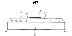
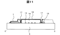
次に、本発明の実施例のタッチパネル400の製造方法を図5ないし図13を用いて説明する。図3のB−B’線に沿った各プロセス段階の断面構造を図5ないし図8に示す。同様に図3のC−C’線に沿った各プロセス段階の断面構造を図9ないし図12に示す。
図5および図9を用いて第1の工程を説明する。
第1の工程では、ガラス基板5上に第1のITO膜14(Indium Tin Oxide)を約15nmの厚さで成膜した後、銀合金膜15を約200nm成膜する。
次に、ホトリソグラフィ工程でレジストパターンを形成し、銀合金膜15をパターニングする。
次に、レジストを剥離除去し、ホトリソグラフィ工程でレジストパターンを形成し第1のITO膜14をパターニングする。
その後、レジストを剥離除去して、図5および図9に示すように、パターンニングされたITO膜14(所謂、Y電極2)と銀合金膜15(所謂、配線6)を形成する。
銀合金膜15は不透明であるため、視認されることを避けるために、後で重ねる液晶表示パネル600の表示領域に掛かる部分からは除去し、周辺配線6のみに形成する。
Next, the manufacturing method of the
The first step will be described with reference to FIGS.
In the first step, a first ITO film 14 (Indium Tin Oxide) is formed on the
Next, a resist pattern is formed by a photolithography process, and the
Next, the resist is peeled and removed, a resist pattern is formed by a photolithography process, and the
Thereafter, the resist is peeled and removed to form a patterned ITO film 14 (so-called Y electrode 2) and a silver alloy film 15 (so-called wiring 6) as shown in FIGS.
Since the
次に、図6および図10を用いて第2の工程を説明する。
第2の工程では、第1のITO膜14と銀合金膜15のパターンを形成した基板上に感光性の層間絶縁膜16を塗布しホトリソグラフィ技術でパターニング加工する。層間絶縁膜16はSiO2を主成分とする膜を1μm以上塗布するのが望ましい。
図10に示すように、周辺部にコンタクトホール17を設ける。また、外部駆動回路との接続に使用する端子接続部では層間絶縁膜パターン16を除去する。
次に、図7および図11を用いて第3の工程を説明する。
第3の工程では、第2のITO膜18を約30nm成膜し、ホトリソグラフィ工程でレジストパターンを形成し、第2のITO膜18をパターニングする。
その後、レジストを剥離除去して、図7および図11に示すように、第2のITO膜18(所謂、X電極1)を形成する。
次に、図8および図12を用いて第4の工程を説明する。
第4の工程では、第2の工程で用いた絶縁膜と同じ膜を最上層保護膜19として再度基板上に塗布し、ホトリソグラフィ工程でパターンを形成する。
以上の工程をもってタッチパネル400が形成される。
Next, a 2nd process is demonstrated using FIG. 6 and FIG.
In the second step, a photosensitive
As shown in FIG. 10, a
Next, a 3rd process is demonstrated using FIG. 7 and FIG.
In the third step, the
Thereafter, the resist is peeled and removed, and a second ITO film 18 (so-called X electrode 1) is formed as shown in FIGS.
Next, a 4th process is demonstrated using FIG. 8 and FIG.
In the fourth process, the same film as the insulating film used in the second process is applied again on the substrate as the uppermost
The
以下、本実施例のタッチパネル400の入力位置の検出動作について簡単に説明する。
本実施例では、X電極1とY電極2に、タッチパネル制御回路60から順次定電流を供給し、X電極1あるいはY電極2を充電し、そして、X電極1あるいはY電極2の電圧が、所定の基準電圧(Vref)に立ち上がるまでの期間(T)を測定する。
例えば、図14に示すように、タッチパネル400が、観察者の指等で触れられていない状態では、前述の期間(T)は、Taとなる。一方、タッチパネル400が、観察者の指35等で触れられた状態では、図13に示すように、X電極1あるいはY電極2の個別電極(1b,2b)に容量(C)が付加されるので、前述の期間(T)は、Taの期間よりも長いTb(Ta<Tb)となる。
一般に、観察者の指35は、X電極1あるいはY電極2の個別電極(1b,2b)の面積よりも大きいので、Taの期間よりも大きい期間(例えば、Tbの期間)は、X電極1あるいはY電極2の複数の電極で検出される。そこで、Taの期間よりも大きい期間が検出された複数の電極位置と、当該電極位置の期間(例えば、Tb)に基づき、セントロイド処理計算により重心位置を求め、入力位置とする。
なお、前述の期間(T)は、例えば、基本クロック(例えば、液晶表示パネル600で使用するドットクロック(CLK))をカウントして、当該カウント数で検出する。
したがって、請求項1に記載の「X電極とY電極との1ライン分の容量」とは、タッチパネル制御回路60から見たインピーダンスの容量成分を意味することにもなる。また、「X電極とY電極との1ライン分の容量が同等」とは、前述の期間(T)、あるいは、前述の期間(T)内のドットクロック(CLK)のカウント数が同等であることも意味している。
さらに、「X電極とY電極との1ライン分の容量が同等」とは、1ライン分の容量が、設計値の±10%以内の値であることを意味している。当然の如く、「前述の期間(T)内のドットクロック(CLK)のカウント数が同等」とは、カウント数が、設計値の±10%以内のカウント数であることを意味している。
Hereinafter, the operation of detecting the input position of the
In this embodiment, a constant current is sequentially supplied to the
For example, as shown in FIG. 14, in a state where the
In general, since the observer's
In the period (T) described above, for example, a basic clock (for example, a dot clock (CLK) used in the liquid crystal display panel 600) is counted and detected by the count number.
Therefore, the “capacity for one line of the X electrode and the Y electrode” described in
Furthermore, “the capacity for one line of the X electrode and the Y electrode is equal” means that the capacity for one line is within ± 10% of the design value. As a matter of course, “the number of counts of the dot clock (CLK) within the above-described period (T) is the same” means that the count is within ± 10% of the design value.
なお、本発明は、入力検出領域の形状、個別電極の形状に限らず、適用可能である。例えば、図15、図16に示すように、X電極1とY電極2とが同一層に形成されるタッチパネルにも適用可能である。
この図15、図16に示すタッチパネルでは、X電極1の個別電極1bと、Y電極2の個別電極2bとは、同層の導電層に分離して形成され、X電極1の交差部1aと、Y電極2の交差部2aとは、異なる導電層に形成される。
図16では、X電極1の交差部1aは、Y電極2の交差部2aよりも上層に形成され、Y電極2の交差部2aと平面的に交差している。X電極1の交差部1aは、層間絶縁膜16に形成されたコンタクトホール36を介してX電極1の個別電極1bと接続される。なお、図16は、図15のA−A’線に沿った断面構造を示す断面図である。
また、前述の実施例では、直交するX方向および、Y方向の電極について記述したが、本発明は、入力位置の検出に用いる電極ライン間の容量差の平均化を目的としたもののため、斜めに交差するものや並走する長さの異なる電極間の容量調整にも有効である。
このように、本実施例によれば、画像情報、文字情報の表示装置用の静電容量結合式入力装置として、検出感度に優れたタッチパネルを生産することが可能となる。
以上、本発明者によってなされた発明を、前記実施例に基づき具体的に説明したが、本
発明は、前記実施例に限定されるものではなく、その要旨を逸脱しない範囲において種々変更可能であることは勿論である。
The present invention is not limited to the shape of the input detection area and the shape of the individual electrodes, and can be applied. For example, as shown in FIGS. 15 and 16, the present invention can be applied to a touch panel in which the
In the touch panel shown in FIGS. 15 and 16, the
In FIG. 16, the intersection 1 a of the
In the above-described embodiment, the electrodes in the X direction and the Y direction which are orthogonal to each other have been described. However, the present invention aims to average the capacitance difference between the electrode lines used for detecting the input position. It is also effective for adjusting the capacitance between electrodes that cross each other and electrodes that run in parallel.
As described above, according to the present embodiment, it is possible to produce a touch panel with excellent detection sensitivity as a capacitive coupling input device for a display device for image information and character information.
As mentioned above, the invention made by the present inventor has been specifically described based on the above embodiments. However, the present invention is not limited to the above embodiments, and various modifications can be made without departing from the scope of the invention. Of course.
1 X電極
2 Y電極
3 入力領域
4 浮遊電極
5 ガラス基板
6 周辺配線
7 接続端子
8 間隔
12 前面保護板
14 第1のITO膜
15 銀合金膜
16 層間絶縁膜
17,36 コンタクトホール
18 第2のITO膜
19 最上層保護膜
30 スペーサ
35 観察者の指
36 コンタクトホール
50 駆動回路
60 タッチパネル制御回路
71,72 フレキシブルプリント基板
300 タッチパネル付き表示装置
400 静電容量結合方式のタッチパネル
501 第1の接着材
502 第2の接着材
600 液晶表示パネル
601,602 偏光板
603 透明導電層
700 バックライト
DESCRIPTION OF SYMBOLS 1 X electrode 2 Y electrode 3 Input area 4 Floating
Claims (19)
前記透明基板に形成された複数のX電極と、
前記透明基板に形成され前記X電極と交差する複数のY電極とを有し、
前記X電極と前記Y電極とは、互いに重なり合う交差部と、2つの交差部間に形成された電極部とを有し、
前記X電極と前記Y電極とは、前記交差部で絶縁膜を介して分離され、
前記電極部は、前記X電極と前記Y電極共に、前記交差部に接続される部分で幅が狭く、前記交差部で挟まれた部分が前記交差部よりも幅が広くなる形状を有し、
前記X電極の1ラインの延在方向の長さに対し、前記Y電極の1ラインの延在方向の長さが短く、
前記X電極の電極部の幅は、前記Y電極の電極部の幅よりも狭く、
前記X電極よりも面積の小さいダミー電極が、前記X電極に近接して形成され、
前記ダミー電極は前記Y電極と重ならないことを特徴とするタッチパネル。 A transparent substrate;
A plurality of X electrodes formed on the transparent substrate ;
A plurality of Y electrodes formed on the transparent substrate and intersecting the X electrodes;
The X electrode and the Y electrode have an intersecting portion overlapping each other and an electrode portion formed between the two intersecting portions,
The X electrode and the Y electrode are separated through an insulating film at the intersection,
The electrode portion has a shape in which both the X electrode and the Y electrode are narrow at a portion connected to the intersection, and a portion sandwiched by the intersection is wider than the intersection.
The length in the extending direction of one line of the Y electrode is shorter than the length in the extending direction of one line of the X electrode,
The width of the electrode portion of the X electrode is narrower than the width of the electrode portion of the Y electrode,
A dummy electrode having a smaller area than the X electrode is formed in proximity to the X electrode ;
The touch panel, wherein the dummy electrode does not overlap the Y electrode .
前記ダミー電極は、前記X電極の電極部と同層に形成された透明導電膜で構成されることを特徴とする請求項1に記載のタッチパネル。 The X electrode and the Y electrode are composed of a transparent conductive film formed with an insulating film interposed therebetween,
The touch panel as set forth in claim 1, wherein the dummy electrode includes a transparent conductive film formed in the same layer as the electrode portion of the X electrode.
前記透明基板に形成された複数のX電極と、
前記透明基板に形成され前記X電極と交差する複数のY電極と、
長辺と短辺とを有する基板とを有し、
前記X電極と前記Y電極とは、互いに重なり合う交差部と、2つの交差部間に形成され前記交差部よりも幅が広い個別電極とを有し、
前記X電極と前記Y電極とは、前記交差部で絶縁膜を介して分離され、
前記X電極は、前記基板の長辺に沿って形成され、
前記Y電極は、前記基板の短辺に沿って形成され、
前記X電極よりも面積が小さく前記Y電極と重ならないダミー電極が、前記X電極に近接して形成され、
前記X電極の個別電極は、前記Y電極の個別電極よりも面積が小さいことを特徴とするタッチパネル。 A transparent substrate;
A plurality of X electrodes formed on the transparent substrate ;
A plurality of Y electrodes formed on the transparent substrate and intersecting the X electrodes;
A substrate having a long side and a short side,
The X electrode and the Y electrode have an intersecting portion that overlaps each other, and an individual electrode that is formed between two intersecting portions and wider than the intersecting portion,
The X electrode and the Y electrode are separated through an insulating film at the intersection,
The X electrode is formed along the long side of the substrate,
The Y electrode is formed along the short side of the substrate,
A dummy electrode having a smaller area than the X electrode and not overlapping with the Y electrode is formed adjacent to the X electrode;
The individual electrode of the X electrode has a smaller area than the individual electrode of the Y electrode.
前記ダミー電極は、前記X電極と同層の透明導電膜で構成されることを特徴とする請求項6に記載のタッチパネル。 The X electrode and the Y electrode are composed of a transparent conductive film formed with an insulating film interposed therebetween,
The touch panel according to claim 6, wherein the dummy electrode is formed of a transparent conductive film in the same layer as the X electrode.
前記透明基板に形成された複数のX電極と、
前記透明基板に形成され前記X電極と交差する複数のY電極とを有し、
前記X電極と前記Y電極とは、互いに重なり合う交差部と、2つの交差部間に形成され前記交差部よりも幅が広い個別電極とを有し、
前記X電極と前記Y電極とは、前記交差部で絶縁膜を介して分離され、
前記X電極よりも面積が小さく前記Y電極と重ならないダミー電極が、前記X電極に近接して形成され、
前記X電極は、n個の前記個別電極を有し、
前記Y電極は、m個の前記個別電極を有し、
前記X電極の個別電極の面積と前記Y電極の個別電極の面積の関係は、m:nであることを特徴とするタッチパネル。 A transparent substrate;
A plurality of X electrodes formed on the transparent substrate ;
A plurality of Y electrodes formed on the transparent substrate and intersecting the X electrodes;
The X electrode and the Y electrode have an intersecting portion that overlaps each other, and an individual electrode that is formed between two intersecting portions and wider than the intersecting portion,
The X electrode and the Y electrode are separated through an insulating film at the intersection,
A dummy electrode having a smaller area than the X electrode and not overlapping with the Y electrode is formed adjacent to the X electrode;
The X electrode has n individual electrodes,
The Y electrode has m individual electrodes,
The relationship between the area of the individual electrode of the X electrode and the area of the individual electrode of the Y electrode is m: n.
前記ダミー電極は、前記X電極と同層の透明導電膜で構成されることを特徴とする請求項11に記載のタッチパネル。 The X electrode and the Y electrode are composed of a transparent conductive film formed with an insulating film interposed therebetween,
The touch panel as set forth in claim 11, wherein the dummy electrode includes a transparent conductive film in the same layer as the X electrode.
前記透明基板に形成された複数のX電極と、
前記透明基板に形成され前記X電極と交差する複数のY電極と、
長辺と短辺とを有する基板とを有し、
前記X電極は、前記基板の長辺に沿って延在し、
前記Y電極は、前記基板の短辺に沿って延在し、
前記X電極と前記Y電極とは、互いに重なり合う交差部と、2つの交差部間に形成された電極部とを有し、
前記X電極と前記Y電極とは、前記交差部で絶縁膜を介して分離され、
前記X電極は、第1の交差部と第2の交差部との間のX電極の幅が、前記第1の交差部と第2の交差部との中間で最大の幅となる形状を有し、
前記X電極と前記Y電極との間には、分割されて複数のダミー電極が形成され、
前記ダミー電極は前記Y電極と重ならないことを特徴とするタッチパネル。 A transparent substrate;
A plurality of X electrodes formed on the transparent substrate ;
A plurality of Y electrodes formed on the transparent substrate and intersecting the X electrodes;
A substrate having a long side and a short side,
The X electrode extends along the long side of the substrate,
The Y electrode extends along the short side of the substrate;
The X electrode and the Y electrode have an intersecting portion overlapping each other and an electrode portion formed between the two intersecting portions,
The X electrode and the Y electrode are separated through an insulating film at the intersection,
The X electrode has a shape in which the width of the X electrode between the first intersecting portion and the second intersecting portion is the maximum width between the first intersecting portion and the second intersecting portion. And
A plurality of dummy electrodes are formed between the X electrode and the Y electrode .
The touch panel, wherein the dummy electrode does not overlap the Y electrode .
Priority Applications (17)
| Application Number | Priority Date | Filing Date | Title |
|---|---|---|---|
| JP2008169816A JP5154316B2 (en) | 2008-06-30 | 2008-06-30 | Touch panel |
| CN2009102031450A CN101620490B (en) | 2008-06-30 | 2009-06-02 | Display device with touch panel |
| CN201110349491.7A CN102339188B (en) | 2008-06-30 | 2009-06-02 | Touch-screen |
| CN201110349807.2A CN102339189B (en) | 2008-06-30 | 2009-06-02 | Touch panel |
| US12/493,391 US8217916B2 (en) | 2008-06-30 | 2009-06-29 | Display device with touch panel |
| US13/542,730 US8890838B2 (en) | 2008-06-30 | 2012-07-06 | Display device with touch panel |
| US14/533,625 US9201555B2 (en) | 2008-06-30 | 2014-11-05 | Display device with touch panel |
| US14/926,972 US9513757B2 (en) | 2008-06-30 | 2015-10-29 | Display device with touch panel |
| US15/338,621 US9740331B2 (en) | 2008-06-30 | 2016-10-31 | Display device with touch panel |
| US15/653,824 US9939954B2 (en) | 2008-06-30 | 2017-07-19 | Touch panel |
| US15/908,897 US10133410B2 (en) | 2008-06-30 | 2018-03-01 | Touch panel having X electrodes and Y electrodes |
| US16/161,144 US10338737B2 (en) | 2008-06-30 | 2018-10-16 | Display device |
| US16/420,488 US10579188B2 (en) | 2008-06-30 | 2019-05-23 | Display device |
| US16/750,194 US10983631B2 (en) | 2008-06-30 | 2020-01-23 | Touch panel |
| US17/203,874 US11353986B2 (en) | 2008-06-30 | 2021-03-17 | Touch panel |
| US17/737,077 US11681392B2 (en) | 2008-06-30 | 2022-05-05 | Capacitive touch panel |
| US18/143,646 US12039128B2 (en) | 2008-06-30 | 2023-05-05 | Touch panel |
Applications Claiming Priority (1)
| Application Number | Priority Date | Filing Date | Title |
|---|---|---|---|
| JP2008169816A JP5154316B2 (en) | 2008-06-30 | 2008-06-30 | Touch panel |
Related Child Applications (1)
| Application Number | Title | Priority Date | Filing Date |
|---|---|---|---|
| JP2012140649A Division JP5373938B2 (en) | 2012-06-22 | 2012-06-22 | Display device |
Publications (3)
| Publication Number | Publication Date |
|---|---|
| JP2010009439A JP2010009439A (en) | 2010-01-14 |
| JP2010009439A5 JP2010009439A5 (en) | 2011-07-21 |
| JP5154316B2 true JP5154316B2 (en) | 2013-02-27 |
Family
ID=41446786
Family Applications (1)
| Application Number | Title | Priority Date | Filing Date |
|---|---|---|---|
| JP2008169816A Active JP5154316B2 (en) | 2008-06-30 | 2008-06-30 | Touch panel |
Country Status (3)
| Country | Link |
|---|---|
| US (13) | US8217916B2 (en) |
| JP (1) | JP5154316B2 (en) |
| CN (3) | CN102339188B (en) |
Cited By (4)
| Publication number | Priority date | Publication date | Assignee | Title |
|---|---|---|---|---|
| JP2012178193A (en) * | 2012-06-22 | 2012-09-13 | Japan Display East Co Ltd | Display device |
| US10656742B2 (en) | 2017-02-03 | 2020-05-19 | Samsung Display Co., Ltd. | Touch sensor and display device having the touch sensor |
| US10732746B2 (en) | 2017-05-15 | 2020-08-04 | Samsung Display Co., Ltd. | Touch sensor and display device including the same |
| US12099671B2 (en) | 2017-05-15 | 2024-09-24 | Samsung Display Co., Ltd. | Touch sensor and display device including the same |
Families Citing this family (85)
| Publication number | Priority date | Publication date | Assignee | Title |
|---|---|---|---|---|
| JP5154316B2 (en) | 2008-06-30 | 2013-02-27 | 株式会社ジャパンディスプレイイースト | Touch panel |
| JP5178379B2 (en) | 2008-07-31 | 2013-04-10 | 株式会社ジャパンディスプレイイースト | Display device |
| TW201040818A (en) * | 2009-05-08 | 2010-11-16 | Sintek Photronic Corp | Capacitive touch panel structure with high optical uniformity |
| TWI386656B (en) * | 2009-07-02 | 2013-02-21 | Novatek Microelectronics Corp | Capacitance measurement circuit and method |
| KR101073333B1 (en) | 2009-08-27 | 2011-10-12 | 삼성모바일디스플레이주식회사 | Touch Screen Panel and fabrication method thereof |
| JP5377279B2 (en) * | 2009-12-28 | 2013-12-25 | 株式会社ジャパンディスプレイ | Capacitance type input device and electro-optical device with input function |
| US9405408B2 (en) | 2010-01-15 | 2016-08-02 | Creator Technology B.V. | Trace pattern for touch-sensing application |
| US9705495B2 (en) | 2010-01-15 | 2017-07-11 | Creator Technology B.V. | Asymmetric sensor pattern |
| US8901944B2 (en) | 2010-01-15 | 2014-12-02 | Cypress Semiconductor Corporation | Lattice structure for capacitance sensing electrodes |
| KR101107173B1 (en) * | 2010-02-11 | 2012-01-25 | 삼성모바일디스플레이주식회사 | Organic light emitting diode display and method for manufacturing the same |
| KR101113450B1 (en) * | 2010-03-12 | 2012-02-29 | 삼성모바일디스플레이주식회사 | Touch Screen Panel |
| KR101726623B1 (en) * | 2010-03-16 | 2017-04-14 | 엘지디스플레이 주식회사 | Touch Panel |
| JP5216041B2 (en) * | 2010-04-07 | 2013-06-19 | ダイキン工業株式会社 | Transparent piezoelectric sheet with frame, each having transparent piezoelectric sheet, touch panel, and electronic device |
| US8363034B2 (en) | 2010-04-14 | 2013-01-29 | Panasonic Corporation | Touch panel device |
| TWM388043U (en) * | 2010-04-28 | 2010-09-01 | Minlead Ltd | Touch control panel |
| JP5513262B2 (en) | 2010-06-02 | 2014-06-04 | 株式会社ジャパンディスプレイ | Display device |
| KR101319347B1 (en) * | 2010-06-10 | 2013-10-16 | 엘지디스플레이 주식회사 | Liquid Crystal Display Panel Associated with Touch Panel |
| US8482546B2 (en) | 2010-06-30 | 2013-07-09 | Cypress Semiconductor Corporation | Self shielding capacitance sensing panel |
| US8698767B2 (en) | 2010-08-19 | 2014-04-15 | Samsung Display Co., Ltd. | Touch screen panel |
| KR101448250B1 (en) * | 2010-08-19 | 2014-10-08 | 삼성디스플레이 주식회사 | Touch Screen Panel |
| TWI423092B (en) * | 2010-10-04 | 2014-01-11 | Au Optronics Corp | Touch panel and repairing method thereof |
| KR101684488B1 (en) * | 2010-11-30 | 2016-12-08 | 닛토덴코 가부시키가이샤 | Display panel device having touch input function |
| TWM422118U (en) * | 2010-12-30 | 2012-02-01 | Egalax Empia Technology Inc | Capacitive touch screen |
| CN103238130B (en) * | 2011-02-04 | 2016-06-29 | 信越聚合物株式会社 | Capacitive sensor sheet and manufacture method thereof |
| KR101634424B1 (en) * | 2011-02-24 | 2016-06-28 | 후지필름 가부시키가이샤 | Electroconductive sheet and touch panel |
| US8638316B2 (en) * | 2011-03-11 | 2014-01-28 | Cypress Semiconductor Corporation | Two prong capacitive sensor pattern |
| JP5480193B2 (en) * | 2011-03-31 | 2014-04-23 | 株式会社ジャパンディスプレイ | Touch panel and display device with touch panel |
| TW201241708A (en) * | 2011-04-07 | 2012-10-16 | Elan Microelectronics Corp | Capacitance sensor structure |
| JP5720816B2 (en) * | 2011-06-24 | 2015-05-20 | 三菱マテリアル株式会社 | Conductive film |
| US8903679B2 (en) | 2011-09-23 | 2014-12-02 | Cypress Semiconductor Corporation | Accuracy in a capacitive sense array |
| US9612265B1 (en) | 2011-09-23 | 2017-04-04 | Cypress Semiconductor Corporation | Methods and apparatus to detect a conductive object |
| JP5806066B2 (en) | 2011-09-30 | 2015-11-10 | 富士フイルム株式会社 | Electrode pattern, touch panel, liquid crystal display device, and organic EL display |
| KR101493556B1 (en) * | 2011-10-27 | 2015-02-16 | 엘지디스플레이 주식회사 | Touch sensor integrated type organic light emitting diode display |
| CN103135831B (en) * | 2011-12-05 | 2016-03-30 | 宏达国际电子股份有限公司 | Contact panel |
| US9323092B2 (en) | 2011-12-05 | 2016-04-26 | Htc Corporation | Touch panel |
| MY167319A (en) * | 2011-12-28 | 2018-08-16 | Sharp Kk | Touch panel and display device with touch panel |
| CN103246409A (en) * | 2012-02-10 | 2013-08-14 | 东莞万士达液晶显示器有限公司 | Touch panel and touch display device |
| WO2013158699A1 (en) * | 2012-04-19 | 2013-10-24 | Elo Touch Solutions, Inc. | Projected capacitive touch sensor with asymmetric bridge pattern |
| US9197208B2 (en) | 2012-04-19 | 2015-11-24 | Elo Touch Solutions, Inc. | Projected capacitive touch sensor with asymmetric bridge pattern |
| KR101373044B1 (en) | 2012-04-19 | 2014-03-11 | 삼성디스플레이 주식회사 | Touch Screen Panel |
| CN102723126B (en) * | 2012-05-09 | 2015-10-21 | 南昌欧菲光科技有限公司 | A kind of patterned transparent conductive film based on random grid |
| KR101916200B1 (en) * | 2012-06-29 | 2018-11-07 | 엘지이노텍 주식회사 | Touch window and manufacturing method thereof |
| FR2993999B1 (en) * | 2012-07-27 | 2014-09-12 | Nanomade Concept | METHOD FOR MANUFACTURING A TRANSPARENT TOUCH SURFACE AND TOUCH SURFACE OBTAINED BY SUCH A METHOD |
| JP5854947B2 (en) * | 2012-08-01 | 2016-02-09 | 株式会社ジャパンディスプレイ | Display device with input device, method for manufacturing the same, and electronic device |
| TW201409092A (en) * | 2012-08-17 | 2014-03-01 | Chunghwa Picture Tubes Ltd | Polarizing plates, touch liquid crystal panel and touch display |
| US20140049271A1 (en) * | 2012-08-20 | 2014-02-20 | Matthew Trend | Self-shielding co-planar touch sensor |
| NO336886B1 (en) * | 2012-08-29 | 2015-11-23 | Aker Subsea As | Shock absorber device for use in the installation of underwater equipment |
| JP5270030B1 (en) * | 2012-09-24 | 2013-08-21 | 日本写真印刷株式会社 | Touch panel and method for manufacturing touch panel |
| US9477362B2 (en) * | 2012-09-26 | 2016-10-25 | Mitsubishi Electric Corporation | Touch screen covered with wiring pattern having first and second layers |
| WO2014050202A1 (en) * | 2012-09-27 | 2014-04-03 | シャープ株式会社 | Touch panel |
| TWI476669B (en) * | 2012-10-03 | 2015-03-11 | Ite Tech Inc | Capacitive touch panel |
| JP6031980B2 (en) * | 2012-12-04 | 2016-11-24 | 三菱電機株式会社 | touch screen |
| TWI466002B (en) * | 2012-12-19 | 2014-12-21 | Chih Chung Lin | Manufacturing method of touch panel |
| US20170192544A9 (en) * | 2013-02-22 | 2017-07-06 | Tpk Touch Solutions Inc. | Touch panel and manufacturing method thereof |
| JP5914403B2 (en) * | 2013-03-29 | 2016-05-11 | 株式会社ジャパンディスプレイ | Display device with touch detection function and electronic device |
| JP2014219816A (en) | 2013-05-08 | 2014-11-20 | 株式会社ジャパンディスプレイ | Display device with touch panel |
| US9495050B1 (en) | 2013-09-10 | 2016-11-15 | Monterey Research, Llc | Sensor pattern with signal-spreading electrodes |
| US8872526B1 (en) | 2013-09-10 | 2014-10-28 | Cypress Semiconductor Corporation | Interleaving sense elements of a capacitive-sense array |
| KR102162912B1 (en) * | 2013-12-06 | 2020-10-07 | 엘지디스플레이 주식회사 | Organic electroluminescent device having touch panel and method for fabricating the same |
| JP5805797B2 (en) * | 2014-01-06 | 2015-11-10 | 株式会社ジャパンディスプレイ | Display device |
| CN103744568A (en) * | 2014-01-13 | 2014-04-23 | 深圳莱宝高科技股份有限公司 | Touch panel and manufacturing method thereof |
| CN103777815B (en) | 2014-01-20 | 2018-01-02 | 北京京东方光电科技有限公司 | A kind of touch control display apparatus and preparation method thereof |
| JP2015152946A (en) * | 2014-02-10 | 2015-08-24 | 大日本印刷株式会社 | Electrode substrate for touch panel, touch panel, and display device |
| TWI537801B (en) * | 2014-03-20 | 2016-06-11 | 原相科技股份有限公司 | Noise-cancelled capacitive touch display apparatus |
| TWI524248B (en) * | 2014-04-03 | 2016-03-01 | 創為精密材料股份有限公司 | Mutual capacitance touch sensitive sensing apparatus and system and method thereof |
| KR101583567B1 (en) * | 2014-04-22 | 2016-01-08 | 주식회사 하이딥 | Touch input device and touch detecting method |
| KR101539330B1 (en) * | 2014-04-30 | 2015-07-30 | 엘지디스플레이 주식회사 | Display Panel For Display Device |
| JP6327925B2 (en) * | 2014-04-30 | 2018-05-23 | 株式会社ワコム | Position detection device |
| KR200480434Y1 (en) | 2014-05-29 | 2016-05-24 | 제이 터치 코퍼레이션 | Double-layer electrode structure for touch-sensitive panel |
| CN104571756B (en) * | 2014-12-04 | 2017-11-10 | 上海天马微电子有限公司 | Touch display panel, driving method thereof and touch device |
| KR20160114510A (en) * | 2015-03-24 | 2016-10-05 | 가부시키가이샤 한도오따이 에네루기 켄큐쇼 | Touch panel |
| TWI567603B (en) * | 2015-04-16 | 2017-01-21 | Au Optronics Corp | Touch display device |
| JP6620025B2 (en) | 2016-01-19 | 2019-12-11 | 株式会社ジャパンディスプレイ | Display device with sensor |
| JP6779762B2 (en) | 2016-11-29 | 2020-11-04 | 株式会社ジャパンディスプレイ | Display device |
| JP2018106057A (en) * | 2016-12-27 | 2018-07-05 | 株式会社ジャパンディスプレイ | Display device and unit register circuit |
| JP6369589B1 (en) * | 2017-03-30 | 2018-08-08 | Smk株式会社 | Capacitive touch panel |
| KR102324218B1 (en) * | 2017-04-14 | 2021-11-10 | 삼성디스플레이 주식회사 | Touch sensor and display device having the same |
| KR102425832B1 (en) | 2017-06-05 | 2022-07-29 | 삼성디스플레이 주식회사 | Touch panel |
| CN107422560A (en) * | 2017-09-04 | 2017-12-01 | 京东方科技集团股份有限公司 | A kind of array base palte, its detection method and display device |
| KR102402040B1 (en) | 2017-12-21 | 2022-05-26 | 삼성디스플레이 주식회사 | Electronic apparatus and method of manufacturing the same |
| CN110032300B (en) * | 2017-12-28 | 2024-02-20 | 天马日本株式会社 | Touch panel and touch panel device |
| CN109634469B (en) * | 2019-02-27 | 2021-01-26 | 京东方科技集团股份有限公司 | Display module, manufacturing method thereof and touch display device |
| US11216140B2 (en) | 2019-04-16 | 2022-01-04 | Elo Touch Solutions, Inc. | PCAP touchscreens with varying ITO dicing patterns |
| JP2021036436A (en) * | 2020-10-13 | 2021-03-04 | 株式会社ジャパンディスプレイ | Display |
| CN112306296B (en) * | 2020-10-29 | 2022-04-15 | 业成科技(成都)有限公司 | Reworking method of touch module |
Family Cites Families (25)
| Publication number | Priority date | Publication date | Assignee | Title |
|---|---|---|---|---|
| US5543588A (en) * | 1992-06-08 | 1996-08-06 | Synaptics, Incorporated | Touch pad driven handheld computing device |
| GB9406702D0 (en) * | 1994-04-05 | 1994-05-25 | Binstead Ronald P | Multiple input proximity detector and touchpad system |
| US7030860B1 (en) | 1999-10-08 | 2006-04-18 | Synaptics Incorporated | Flexible transparent touch sensing system for electronic devices |
| US6593916B1 (en) * | 2000-11-03 | 2003-07-15 | James L. Aroyan | Touchscreen having multiple parallel connections to each electrode in a series resistor chain on the periphery of the touch area |
| JP2003196030A (en) * | 2001-12-28 | 2003-07-11 | Kawaguchiko Seimitsu Co Ltd | Touch panel |
| JP2004361919A (en) * | 2003-05-12 | 2004-12-24 | Seiko Epson Corp | Electro-optical panel driving circuit and electro-optical device provided therewith, and electronic equipment provided therewith |
| GB0319714D0 (en) * | 2003-08-21 | 2003-09-24 | Philipp Harald | Anisotropic touch screen element |
| JP4691890B2 (en) * | 2004-03-19 | 2011-06-01 | セイコーエプソン株式会社 | Electro-optical device and electronic apparatus |
| JP4239890B2 (en) * | 2004-04-26 | 2009-03-18 | セイコーエプソン株式会社 | Organic EL devices, electronic devices |
| US7508462B2 (en) * | 2005-05-18 | 2009-03-24 | Sony Corporation | Electro-optical device and electronic equipment |
| EP1892609A4 (en) * | 2005-05-26 | 2013-03-27 | Gunze Kk | Transparent planar body and transparent touch switch |
| TW200709024A (en) * | 2005-08-31 | 2007-03-01 | Elan Microelectronics Corp | Touch sensor |
| US8111243B2 (en) * | 2006-03-30 | 2012-02-07 | Cypress Semiconductor Corporation | Apparatus and method for recognizing a tap gesture on a touch sensing device |
| JP4687561B2 (en) * | 2006-05-17 | 2011-05-25 | パナソニック株式会社 | Touch panel |
| US8040321B2 (en) * | 2006-07-10 | 2011-10-18 | Cypress Semiconductor Corporation | Touch-sensor with shared capacitive sensors |
| JP2008097283A (en) * | 2006-10-11 | 2008-04-24 | Hosiden Corp | Touch panel input device |
| KR101297387B1 (en) * | 2006-11-09 | 2013-08-19 | 삼성디스플레이 주식회사 | Liquid crystal display associated with touch panel |
| JP2008129708A (en) * | 2006-11-17 | 2008-06-05 | Alps Electric Co Ltd | Transparent touch panel and its manufacturing method |
| US8072429B2 (en) * | 2006-12-22 | 2011-12-06 | Cypress Semiconductor Corporation | Multi-axial touch-sensor device with multi-touch resolution |
| US8674950B2 (en) * | 2007-09-06 | 2014-03-18 | Cypress Semiconductor Corporation | Dual-sensing-mode touch-sensor device |
| CN100495139C (en) | 2007-10-10 | 2009-06-03 | 友达光电股份有限公司 | Touching control panel and its manufacturing method |
| JP5154316B2 (en) * | 2008-06-30 | 2013-02-27 | 株式会社ジャパンディスプレイイースト | Touch panel |
| US7982723B2 (en) * | 2008-09-18 | 2011-07-19 | Stmicroelectronics Asia Pacific Pte. Ltd. | Multiple touch location in a three dimensional touch screen sensor |
| JP5138529B2 (en) * | 2008-10-03 | 2013-02-06 | 株式会社ジャパンディスプレイイースト | Touch panel |
| JP5528926B2 (en) | 2010-07-09 | 2014-06-25 | 株式会社ジャパンディスプレイ | Detection device and display device |
-
2008
- 2008-06-30 JP JP2008169816A patent/JP5154316B2/en active Active
-
2009
- 2009-06-02 CN CN201110349491.7A patent/CN102339188B/en active Active
- 2009-06-02 CN CN201110349807.2A patent/CN102339189B/en active Active
- 2009-06-02 CN CN2009102031450A patent/CN101620490B/en active Active
- 2009-06-29 US US12/493,391 patent/US8217916B2/en active Active
-
2012
- 2012-07-06 US US13/542,730 patent/US8890838B2/en active Active
-
2014
- 2014-11-05 US US14/533,625 patent/US9201555B2/en active Active
-
2015
- 2015-10-29 US US14/926,972 patent/US9513757B2/en active Active
-
2016
- 2016-10-31 US US15/338,621 patent/US9740331B2/en active Active
-
2017
- 2017-07-19 US US15/653,824 patent/US9939954B2/en active Active
-
2018
- 2018-03-01 US US15/908,897 patent/US10133410B2/en active Active
- 2018-10-16 US US16/161,144 patent/US10338737B2/en active Active
-
2019
- 2019-05-23 US US16/420,488 patent/US10579188B2/en active Active
-
2020
- 2020-01-23 US US16/750,194 patent/US10983631B2/en active Active
-
2021
- 2021-03-17 US US17/203,874 patent/US11353986B2/en active Active
-
2022
- 2022-05-05 US US17/737,077 patent/US11681392B2/en active Active
-
2023
- 2023-05-05 US US18/143,646 patent/US12039128B2/en active Active
Cited By (7)
| Publication number | Priority date | Publication date | Assignee | Title |
|---|---|---|---|---|
| JP2012178193A (en) * | 2012-06-22 | 2012-09-13 | Japan Display East Co Ltd | Display device |
| US10656742B2 (en) | 2017-02-03 | 2020-05-19 | Samsung Display Co., Ltd. | Touch sensor and display device having the touch sensor |
| US11099699B2 (en) | 2017-02-03 | 2021-08-24 | Samsung Display Co., Ltd. | Touch sensor and display device having the touch sensor |
| US10732746B2 (en) | 2017-05-15 | 2020-08-04 | Samsung Display Co., Ltd. | Touch sensor and display device including the same |
| US11182005B2 (en) | 2017-05-15 | 2021-11-23 | Samsung Display Co., Ltd. | Touch sensor and display device including the same |
| US11714503B2 (en) | 2017-05-15 | 2023-08-01 | Samsung Display Co., Ltd. | Touch sensor and display device including the same |
| US12099671B2 (en) | 2017-05-15 | 2024-09-24 | Samsung Display Co., Ltd. | Touch sensor and display device including the same |
Also Published As
Similar Documents
| Publication | Publication Date | Title |
|---|---|---|
| JP5154316B2 (en) | Touch panel | |
| JP5033078B2 (en) | Display device | |
| JP5138529B2 (en) | Touch panel | |
| JP5178590B2 (en) | Touch panel | |
| JP5133204B2 (en) | Touch panel | |
| JP5408681B2 (en) | Display device | |
| JP5063561B2 (en) | Touch panel | |
| JP2011186623A (en) | Display device with touch panel | |
| JP5373938B2 (en) | Display device | |
| JP5669909B2 (en) | Display device |
Legal Events
| Date | Code | Title | Description |
|---|---|---|---|
| A711 | Notification of change in applicant |
Free format text: JAPANESE INTERMEDIATE CODE: A712 Effective date: 20110218 |
|
| RD03 | Notification of appointment of power of attorney |
Free format text: JAPANESE INTERMEDIATE CODE: A7423 Effective date: 20110218 |
|
| A521 | Request for written amendment filed |
Free format text: JAPANESE INTERMEDIATE CODE: A523 Effective date: 20110607 |
|
| A621 | Written request for application examination |
Free format text: JAPANESE INTERMEDIATE CODE: A621 Effective date: 20110607 |
|
| A977 | Report on retrieval |
Free format text: JAPANESE INTERMEDIATE CODE: A971007 Effective date: 20120413 |
|
| A131 | Notification of reasons for refusal |
Free format text: JAPANESE INTERMEDIATE CODE: A131 Effective date: 20120424 |
|
| A521 | Request for written amendment filed |
Free format text: JAPANESE INTERMEDIATE CODE: A523 Effective date: 20120622 |
|
| TRDD | Decision of grant or rejection written | ||
| A01 | Written decision to grant a patent or to grant a registration (utility model) |
Free format text: JAPANESE INTERMEDIATE CODE: A01 Effective date: 20121120 |
|
| A61 | First payment of annual fees (during grant procedure) |
Free format text: JAPANESE INTERMEDIATE CODE: A61 Effective date: 20121205 |
|
| FPAY | Renewal fee payment (event date is renewal date of database) |
Free format text: PAYMENT UNTIL: 20151214 Year of fee payment: 3 |
|
| R150 | Certificate of patent or registration of utility model |
Free format text: JAPANESE INTERMEDIATE CODE: R150 Ref document number: 5154316 Country of ref document: JP Free format text: JAPANESE INTERMEDIATE CODE: R150 |
|
| R250 | Receipt of annual fees |
Free format text: JAPANESE INTERMEDIATE CODE: R250 |
|
| R250 | Receipt of annual fees |
Free format text: JAPANESE INTERMEDIATE CODE: R250 |
|
| R250 | Receipt of annual fees |
Free format text: JAPANESE INTERMEDIATE CODE: R250 |
|
| R250 | Receipt of annual fees |
Free format text: JAPANESE INTERMEDIATE CODE: R250 |
|
| R250 | Receipt of annual fees |
Free format text: JAPANESE INTERMEDIATE CODE: R250 |
|
| R250 | Receipt of annual fees |
Free format text: JAPANESE INTERMEDIATE CODE: R250 |
|
| S531 | Written request for registration of change of domicile |
Free format text: JAPANESE INTERMEDIATE CODE: R313531 |
|
| S533 | Written request for registration of change of name |
Free format text: JAPANESE INTERMEDIATE CODE: R313533 |
|
| R350 | Written notification of registration of transfer |
Free format text: JAPANESE INTERMEDIATE CODE: R350 |
|
| R250 | Receipt of annual fees |
Free format text: JAPANESE INTERMEDIATE CODE: R250 |
|
| R250 | Receipt of annual fees |
Free format text: JAPANESE INTERMEDIATE CODE: R250 |
|
| S111 | Request for change of ownership or part of ownership |
Free format text: JAPANESE INTERMEDIATE CODE: R313117 |
|
| R350 | Written notification of registration of transfer |
Free format text: JAPANESE INTERMEDIATE CODE: R350 |
|
| R250 | Receipt of annual fees |
Free format text: JAPANESE INTERMEDIATE CODE: R250 |
|
| S111 | Request for change of ownership or part of ownership |
Free format text: JAPANESE INTERMEDIATE CODE: R313113 |
|
| R350 | Written notification of registration of transfer |
Free format text: JAPANESE INTERMEDIATE CODE: R350 |