JP5147331B2 - Laser light control apparatus and image forming apparatus - Google Patents
Laser light control apparatus and image forming apparatus Download PDFInfo
- Publication number
- JP5147331B2 JP5147331B2 JP2007214744A JP2007214744A JP5147331B2 JP 5147331 B2 JP5147331 B2 JP 5147331B2 JP 2007214744 A JP2007214744 A JP 2007214744A JP 2007214744 A JP2007214744 A JP 2007214744A JP 5147331 B2 JP5147331 B2 JP 5147331B2
- Authority
- JP
- Japan
- Prior art keywords
- laser light
- laser
- lens
- optical element
- detection
- Prior art date
- Legal status (The legal status is an assumption and is not a legal conclusion. Google has not performed a legal analysis and makes no representation as to the accuracy of the status listed.)
- Expired - Fee Related
Links
Images


Classifications
-
- G—PHYSICS
- G02—OPTICS
- G02B—OPTICAL ELEMENTS, SYSTEMS OR APPARATUS
- G02B26/00—Optical devices or arrangements for the control of light using movable or deformable optical elements
- G02B26/08—Optical devices or arrangements for the control of light using movable or deformable optical elements for controlling the direction of light
- G02B26/10—Scanning systems
-
- H—ELECTRICITY
- H01—ELECTRIC ELEMENTS
- H01S—DEVICES USING THE PROCESS OF LIGHT AMPLIFICATION BY STIMULATED EMISSION OF RADIATION [LASER] TO AMPLIFY OR GENERATE LIGHT; DEVICES USING STIMULATED EMISSION OF ELECTROMAGNETIC RADIATION IN WAVE RANGES OTHER THAN OPTICAL
- H01S5/00—Semiconductor lasers
- H01S5/06—Arrangements for controlling the laser output parameters, e.g. by operating on the active medium
- H01S5/068—Stabilisation of laser output parameters
- H01S5/0683—Stabilisation of laser output parameters by monitoring the optical output parameters
-
- G—PHYSICS
- G02—OPTICS
- G02B—OPTICAL ELEMENTS, SYSTEMS OR APPARATUS
- G02B26/00—Optical devices or arrangements for the control of light using movable or deformable optical elements
- G02B26/08—Optical devices or arrangements for the control of light using movable or deformable optical elements for controlling the direction of light
- G02B26/10—Scanning systems
- G02B26/12—Scanning systems using multifaceted mirrors
- G02B26/127—Adaptive control of the scanning light beam, e.g. using the feedback from one or more detectors
-
- G—PHYSICS
- G03—PHOTOGRAPHY; CINEMATOGRAPHY; ANALOGOUS TECHNIQUES USING WAVES OTHER THAN OPTICAL WAVES; ELECTROGRAPHY; HOLOGRAPHY
- G03G—ELECTROGRAPHY; ELECTROPHOTOGRAPHY; MAGNETOGRAPHY
- G03G15/00—Apparatus for electrographic processes using a charge pattern
-
- G—PHYSICS
- G03—PHOTOGRAPHY; CINEMATOGRAPHY; ANALOGOUS TECHNIQUES USING WAVES OTHER THAN OPTICAL WAVES; ELECTROGRAPHY; HOLOGRAPHY
- G03G—ELECTROGRAPHY; ELECTROPHOTOGRAPHY; MAGNETOGRAPHY
- G03G15/00—Apparatus for electrographic processes using a charge pattern
- G03G15/04—Apparatus for electrographic processes using a charge pattern for exposing, i.e. imagewise exposure by optically projecting the original image on a photoconductive recording material
-
- H—ELECTRICITY
- H01—ELECTRIC ELEMENTS
- H01S—DEVICES USING THE PROCESS OF LIGHT AMPLIFICATION BY STIMULATED EMISSION OF RADIATION [LASER] TO AMPLIFY OR GENERATE LIGHT; DEVICES USING STIMULATED EMISSION OF ELECTROMAGNETIC RADIATION IN WAVE RANGES OTHER THAN OPTICAL
- H01S5/00—Semiconductor lasers
-
- H—ELECTRICITY
- H04—ELECTRIC COMMUNICATION TECHNIQUE
- H04N—PICTORIAL COMMUNICATION, e.g. TELEVISION
- H04N1/00—Scanning, transmission or reproduction of documents or the like, e.g. facsimile transmission; Details thereof
- H04N1/40—Picture signal circuits
- H04N1/40025—Circuits exciting or modulating particular heads for reproducing continuous tone value scales
-
- H—ELECTRICITY
- H01—ELECTRIC ELEMENTS
- H01S—DEVICES USING THE PROCESS OF LIGHT AMPLIFICATION BY STIMULATED EMISSION OF RADIATION [LASER] TO AMPLIFY OR GENERATE LIGHT; DEVICES USING STIMULATED EMISSION OF ELECTROMAGNETIC RADIATION IN WAVE RANGES OTHER THAN OPTICAL
- H01S5/00—Semiconductor lasers
- H01S5/005—Optical components external to the laser cavity, specially adapted therefor, e.g. for homogenisation or merging of the beams or for manipulating laser pulses, e.g. pulse shaping
-
- H—ELECTRICITY
- H01—ELECTRIC ELEMENTS
- H01S—DEVICES USING THE PROCESS OF LIGHT AMPLIFICATION BY STIMULATED EMISSION OF RADIATION [LASER] TO AMPLIFY OR GENERATE LIGHT; DEVICES USING STIMULATED EMISSION OF ELECTROMAGNETIC RADIATION IN WAVE RANGES OTHER THAN OPTICAL
- H01S5/00—Semiconductor lasers
- H01S5/06—Arrangements for controlling the laser output parameters, e.g. by operating on the active medium
- H01S5/068—Stabilisation of laser output parameters
- H01S5/06825—Protecting the laser, e.g. during switch-on/off, detection of malfunctioning or degradation
Landscapes
- Physics & Mathematics (AREA)
- General Physics & Mathematics (AREA)
- Optics & Photonics (AREA)
- Condensed Matter Physics & Semiconductors (AREA)
- Electromagnetism (AREA)
- Engineering & Computer Science (AREA)
- Multimedia (AREA)
- Signal Processing (AREA)
- Facsimile Scanning Arrangements (AREA)
- Mechanical Optical Scanning Systems (AREA)
- Laser Beam Printer (AREA)
Description
本発明は、画像形成装置に用いて好適なレーザ光制御装置及び画像形成装置に関する。 The present invention relates to a laser light control device and an image forming apparatus suitable for use in an image forming apparatus.
半導体レーザの光出力特性は周囲の温度の変化に敏感なため、一定電流で駆動していても周囲の温度変化又は自己発熱等により、その光出力は大きく変動してしまう。この光出力の温度依存性に対応するために、一般に半導体レーザのパッケージ内にモニタダイオードと呼ばれるフォトダイオード(PD)が組み込まれている。これにより半導体レーザのバック光の光出力をモニタして駆動電流を制御し、光出力を一定に保つことができるように制御している。このようなフィードバック機構を持つ半導体レーザの光量制御を行う駆動回路をAPC(Auto Power Control)回路(自動光出力制御回路)と呼んでいる。 Since the light output characteristics of a semiconductor laser are sensitive to changes in the ambient temperature, the light output greatly fluctuates due to changes in the ambient temperature or self-heating even when driven with a constant current. In order to cope with the temperature dependence of the light output, a photodiode (PD) called a monitor diode is generally incorporated in a semiconductor laser package. As a result, the optical output of the back light of the semiconductor laser is monitored to control the drive current so that the optical output can be kept constant. A drive circuit for controlling the light amount of a semiconductor laser having such a feedback mechanism is called an APC (Auto Power Control) circuit (automatic light output control circuit).
さて、レーザ走査装置を使用したプリンタ等における画像データに応じて半導体レーザをオン/オフさせるような駆動回路においては、レーザ点灯の時間が不規則なため、一般に画像領域外で一定時間レーザを点灯させてAPC制御を行うことが一般的である。 Now, in a drive circuit that turns on / off a semiconductor laser in accordance with image data in a printer using a laser scanning device, the laser lighting time is irregular, so the laser is generally turned on for a certain time outside the image area. In general, APC control is performed.
パッケージ内にフォトダイオードを一体に組み込んだフォトダイオード一体型レーザダイオードをレーザ走査装置のAPC回路に用いることは、以下の点で有利である。レーザダイオードと別体に構成されるディスクリート型のフォトダイオードを用いて発光出力をモニタする構成に比較して、配設スペースが低減でき、かつ独立した配線が不要になり、レーザ走査装置の構成の簡略化、低コスト化を図ることができる。 The use of a photodiode integrated laser diode in which a photodiode is integrated in a package for an APC circuit of a laser scanning device is advantageous in the following points. Compared to a configuration in which the light emission output is monitored using a discrete type photodiode configured separately from the laser diode, the arrangement space can be reduced and an independent wiring is not required. Simplification and cost reduction can be achieved.
しかしながら、上記の構成は、半導体レーザ自身の温度の変化によっても、パッケージ中のフォトダイオードが受光する半導体レーザのバック光の光量が微小に変化するため、APC制御を行っても精度の高いレーザ光量制御が実現していなかった。 However, in the above configuration, the amount of the back light of the semiconductor laser received by the photodiode in the package changes minutely even when the temperature of the semiconductor laser itself changes. Control was not realized.
そこで、半導体レーザのパッケージ外に射出されるフォワード光をAPC制御に用いる系が知られている(例えば、特許文献1参照)。
しかしながら、上記の構成は、レーザ光の主走査位置の検出(画像書き出しの基準信号:BD信号)をするフォトダイオードと、光量を検出させるフォトダイオードを各々設置しなければならなかった。 However, in the above configuration, it is necessary to install a photodiode for detecting the main scanning position of the laser beam (reference signal for image writing: BD signal) and a photodiode for detecting the amount of light.
そこで、単一のフォトダイオードでレーザ光の主走査位置の検出(画像書き出しの基準信号:BD信号)をするフォトダイオードと光量を検出させるフォトダイオードとを兼用させるのが好ましい。ところが、レーザ光の主走査方向のフォトダイオードを設置できる位置は限られ、設置したフォトダイオードの受光面の占有する領域が小さく、レーザ光の光量を検知するタイミングは、1ラインの走査の中でレーザ光がフォトダイオードを通過する時間となる。そのため、フォトダイオードでレーザ光の光量を検知する時間は非常に短い。このような構成で、フォトダイオードの応答性が低かったり、APC制御の収束に時間を要したりする場合には、レーザ光の光量を正確に検知することが出来ず、安定したフィードバック制御が困難なものとなる。 Therefore, it is preferable to use both a photodiode for detecting the main scanning position of the laser beam (reference signal for image writing: BD signal) and a photodiode for detecting the amount of light with a single photodiode. However, the position where the photodiode in the main scanning direction of the laser light can be installed is limited, the area occupied by the light receiving surface of the installed photodiode is small, and the timing for detecting the amount of laser light is one line of scanning. It is time for the laser light to pass through the photodiode. Therefore, the time for detecting the amount of laser light by the photodiode is very short. With such a configuration, when the response of the photodiode is low or it takes time to converge the APC control, the amount of laser light cannot be accurately detected, and stable feedback control is difficult. It will be something.
本発明の目的は、APC制御精度の向上並びに制御時間の短縮を可能とする画像形成装置に用いて好適なレーザ光制御装置及び画像形成装置を提供することにある。 An object of the present invention is to provide a laser light control apparatus and an image forming apparatus suitable for use in an image forming apparatus that can improve APC control accuracy and shorten control time.
上記目的を達成するために、本発明のレーザ光制御装置は、感光体上に静電潜像を形成するために前記感光体を露光するレーザ光を出射する半導体レーザと、前記半導体レーザから出射されたレーザ光が前記感光体上を走査するように前記レーザ光を偏向する偏向手段と、前記偏向手段によって偏向されたレーザ光が入射する複合機能光学素子と、前記複合機能光学素子を通過したレーザ光を検出する検出手段と、前記検出手段の検出結果に基づいて、半導体レーザから出射される前記レーザ光の光量及び前記レーザ光が前記感光体上を走査する走査方向における前記静電潜像の書き出し位置を制御する制御手段と、を備え、前記複合機能光学素子は、前記偏向手段によって偏向されて前記複合機能光学素子を通過したレーザ光が前記検出手段に入射するように、前記複合機能光学素子に入射するレーザ光の走査方向と垂直な方向に前記レーザ光を屈折させる屈折力を有する第1の特性を有する第1のレンズ部と、前記偏向手段によって偏向されて前記複合機能光学素子を走査するように当該複合機能光学素子に入射するレーザ光を前記検出手段の検出面上に静止させる第2の特性を有する第2のレンズ部と、を有し、前記第1のレンズ部及び第2のレンズ部は前記複合機能光学素子に入射するレーザ光の走査方向において並べて配置され、前記制御手段は、前記第1のレンズ部を通過して前記検出手段によって検出されるレーザ光の検出結果に基づいて前記静電潜像の書き出し位置を制御し、前記第2のレンズ部を通過して前記検出手段によって検出されるレーザ光の検出結果に基づいて前記レーザ光の光量を制御することを特徴とする。 To achieve the above object, Les laser light control device of the present invention includes a semiconductor laser which emits a laser beam for exposing said photosensitive member to form an electrostatic latent image on the photosensitive member, said semiconductor laser Deflecting means for deflecting the laser light so that the laser light emitted from the photosensitive member scans the photosensitive member, a composite functional optical element on which the laser light deflected by the deflecting means is incident, and the composite functional optical element Based on the detection result of the laser beam that has passed, and the detection result of the detection unit, the amount of the laser beam emitted from the semiconductor laser and the electrostatic force in the scanning direction in which the laser beam scans on the photoconductor Control means for controlling the writing position of the latent image, and the composite function optical element is configured such that the laser beam deflected by the deflection means and passed through the composite function optical element is the detection hand. A first lens unit having a first characteristic having a refractive power that refracts the laser beam in a direction perpendicular to a scanning direction of the laser beam incident on the composite functional optical element, And a second lens unit having a second characteristic that causes the laser light incident on the composite function optical element to be stationary on the detection surface of the detection means so as to scan the composite function optical element. The first lens portion and the second lens portion are arranged side by side in the scanning direction of the laser light incident on the composite functional optical element, and the control means passes through the first lens portion and performs the detection. Based on the detection result of the laser light detected by the means, the writing position of the electrostatic latent image is controlled, and the detection result of the laser light detected by the detection means after passing through the second lens unit Zui with and controlling the light amount of the laser light.
本発明の画像形成装置は、上記レーザ光制御装置を備えることを特徴とする。 An image forming apparatus according to the present invention includes the laser light control device.
本発明によれば、レーザの発光量を受光するフォトダイオードの応答性の低さや、APC制御の収束時間不足によるレーザ光量制御の精度低下を防止し、さらに、レーザ光の過剰発光を防止することができる。 According to the present invention, it is possible to prevent low response of a photodiode that receives the light emission amount of a laser, a decrease in accuracy of laser light amount control due to insufficient convergence time of APC control, and further prevention of excessive emission of laser light. Can do.
<第1の実施の形態>
図1は、本発明の実施の形態に係るレーザ光制御装置を備える画像形成装置の構成を概略的に示す図である。
<First Embodiment>
FIG. 1 is a diagram schematically showing a configuration of an image forming apparatus including a laser light control device according to an embodiment of the present invention.
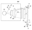
図1において、レーザ出力ユニット200は、半導体レーザであるレーザダイオード8、コリメータレンズ21、スリット22、回転多面鏡(ポリゴンミラー)23、走査レンズ24,25より構成される。
In FIG. 1, a
レーザダイオード8は、所定光量の光で発光させるために、後述する図2のレーザ駆動回路300(レーザ光制御装置)によって発光駆動される。レーザダイオード8から出射されたレーザ光は、コリメータレンズ21、スリット22を通って回転多面鏡23に到達する。回転多面鏡23は、スキャナモータを含む回転多面鏡駆動回路(不図示)によって等角速度で回転している。回転多面鏡23に到達したレーザ光は、回転多面鏡23によって偏向走査され、走査レンズ24,25によって、感光ドラム(像担持体)27上におけるビーム走査の線速度が等速となるように変更される。レーザ光が回転多面鏡23によって偏向走査される面を主走査面、走査レンズ24,25の光軸に対して垂直でかつ主走査面と平行な方向を主走査方向と呼ぶ。また、主走査方向に対して略垂直な方向を副走査方向と呼ぶ。感光ドラム27は、主走査方向aを有する。
The
また、感光ドラム27の非画像領域に相当する位置に、走査レンズ24,25を通ったレーザ光を受光できる本発明の特徴である検出センサ9(検出手段)が設けられている。検出センサ9は、フォトダイオードから成る。検出センサ9には、BDスリット29、並びに複数の異なる光学特性を有する複合機能光学素子としての、BDレンズ30及びAPC用レンズ31を介してレーザ光が導光される。BDスリット29は、感光ドラム27と等価な位置に配置されており、走査レンズ24,25を通ったレーザ光はBDスリット29上でスポット状に集光されている。そしてその後ろに配置されたBDレンズ30によってレーザ光が検出センサ9に導光される。画像領域では、レーザ光は、走査レンズ24,25を通過した後、反射ミラー26を経由して感光ドラム27上を走査することにより潜像を形成する。感光ドラム27に形成された潜像は、トナーで現像後、用紙に転写・定着することにより画像形成される。
Further, a detection sensor 9 (detection means) that is a feature of the present invention is provided at a position corresponding to the non-image area of the
尚、コリメータレンズ21は、レーザ光を平行光とし、スリット22は、平行光の光束幅を所望の幅に制限する。
The
[レーザ駆動回路の動作概要]
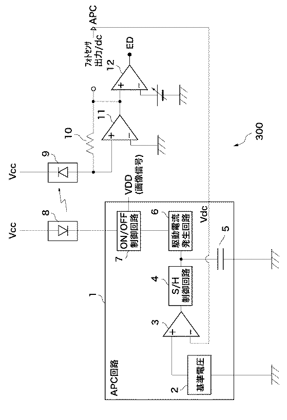
図2は、図1のレーザダイオード8を発光駆動するレーザ駆動回路の内部構成を示すブロック図である。
[Overview of laser drive circuit operation]
FIG. 2 is a block diagram showing an internal configuration of a laser driving circuit that drives the
図2において、レーザ駆動回路300は、レーザダイオードの光量を制御する自動光出力制御(APC:Auto Power Control)とレーザ光の主走査位置の検出を行う。
In FIG. 2, a
レーザ駆動回路300は、APC回路1、レーザダイオード8、検出センサ9、抵抗10、差動増幅器11,12などにより構成される。
The
APC回路1は、フィードバック制御手段として、基準電圧発生回路2、サンプル・ホールド(以下、「S/H」と略す)制御回路4、S/Hコンデンサ5、駆動電流発生回路6、ON/OFF制御回路7より構成される。
The
検出センサ9は、レーザダイオード8から出力されるレーザ光を検出(モニタ)しレーザ光の強度(光量)に応じた電流を出力(信号出力)する。
The
検出センサ9から出力された電流は、差動増幅器12で、基準電圧Vref−1と比較され、基準電圧Vref−1を上回ると画像書き出しの基準信号に使用されるBD信号を生成する。
The current output from the
また、検出センサ9から出力される電流は、抵抗10によりAPC用検知電圧Vdtcとして出力される。出力されたVdtcは、基準電圧発生回路2で生成される基準電圧とともに差動増幅器3に入力され、両者の極性を含む差分が増幅される。
The current output from the
S/H制御回路4は、サンプル・ホールド用のコンデンサ5で、不示図のエンジン制御回路から入力されるS/H制御信号が、サンプルを要求する時には、差動増幅器3の出力信号に応じてS/H制御回路4にてS/Hコンデンサ5に充放電電流を入出力する。また、ホールドを要求する時には、S/H制御回路4とS/Hコンデンサ5間を開放するように制御する。
The S /
S/H制御信号によりサンプル要求がされると、差動増幅器3に入力されたPD電圧信号(APC用検知電圧Vdtc)と基準電圧の差分に応じた信号が増幅され、S/H制御回路4に入力される。
When a sample request is made by the S / H control signal, a signal corresponding to the difference between the PD voltage signal (APC detection voltage Vdtc) input to the
Vdtcが基準電圧より大きいとき、S/Hコンデンサ5からS/H制御回路4を介して差動増幅器出力が放電電流を吸い込む。Vdtcが基準電圧より小さいとき、S/H制御回路4を介してS/Hコンデンサ5へ、差動増幅器出力が充電電流を出力する。Vdtcが基準電圧と等しい場合、充放電は行われない。
When Vdtc is larger than the reference voltage, the differential amplifier output absorbs the discharge current from the S /
S/Hコンデンサ5の両端の電圧は、レーザダイオード駆動電流発生回路6に入力され、S/Hコンデンサ5の両端の電圧に応じたレーザダイオード8を駆動する電流値を決定する。不示図の画像制御回路から入力される画像信号を受信し、ビデオ(以下VDOと略す)信号を、駆動電流発生回路6にて決定された駆動電流値を以って、VDO信号にてオン・オフ駆動された発光動作をレーザダイオード8で行う。
The voltage at both ends of the S /
[検出センサ9の説明]
以下、検出センサ9の構成を図1を参照しながら説明する。本実施の形態では、複合機能光学素子として、主走査方向の画像書き出し位置制御を行うための画像書き出し基準信号(BD信号)を生成するのに使用するBDレンズ30と光量制御を行うのに使用するAPC用レンズ31を図5で示すように一体成型として構成する。尚、検出センサ9にレーザ光を入射できる構成であれば、複合機能光学素子は一体成型に限られるものではない。
[Description of detection sensor 9]
Hereinafter, the configuration of the
第1の光学特性を有するBDレンズ30は、少なくともその副走査方向の形状が、BDミラー28の反射面と検出センサ9とを光学的に略共役な関係となるような屈折力に設定している。それによって、例えばBDミラー28の取り付け時に、副走査方向に対して角度誤差があったとしてもレーザ光が検出センサ9に導光される。また、第2の光学特性を有するAPC用レンズ31は、少なくともその主走査方向の形状が、回転多面鏡23で偏向走査されたレーザ光がAPCレンズ31に入射し、検出センサ9に到達する位置が、その走査の間略静止するような屈折力に設定している。つまり、第1の光学特性と第2の光学特性は異なるものである。
The
図1において、IはBD検知時のレーザ光の様子を示している。IIは、BD検知後所定時間経過後にAPCレンズ31に入射するレーザ光の主光線を示し、IIIは更に所定時間経過後にAPCレンズ31に入射するレーザ光の主光線を示している。
In FIG. 1, I indicates the state of the laser beam at the time of BD detection. II indicates a chief ray of laser light incident on the
APCレンズ31は、少なくともその主走査方向の形状が、前記主光線IIとIIIの延長線が交わる点Aと検出センサ9とが光学的に略共役な関係となるような屈折力に設定にされている。そうすることによって、回転多面鏡23で偏向走査されたレーザ光がAPCレンズ31上を走査し検出センサ9に到達する位置を略静止させることが可能となる。
The
また、BDミラー面28は、回転多面鏡23によって偏向され、走査レンズ24,25を通過したレーザ光を反射して検出センサ9で検知させる。
The
以上のことより、回転多面鏡23で反射され、走査レンズ24,25を通過したレーザ光は、まず、BDレンズ30で集光され、検出センサ9により検知される。検知した光を基に画像書き出しタイミングを生み出す画像書き出しの基準信号(BD信号)を生成する。
From the above, the laser light reflected by the
次に、APC用レンズ31により入射したレーザ光が、検出センサ9上で略静止する。略静止したレーザ光を先述のAPC回路1によりレーザ光の制御を行う。また、光路の途中にあるスリット29は、一体成型したBDレンズ30とAPC用レンズ31が異なる形状なので、つなぎめに発生するフレアを防止する役割がある。
Next, the laser light incident by the
これにより、レーザ駆動回路300は、画像書き出しの基準信号制御を先に行うことで、検出センサ9の信号開始部を用い、APC制御には、検出センサ9の信号開始部以降の信号安定部を用いることになる。
Thereby, the
図5に、複合機能光学素子として、一体成形で構成されたBDレンズ30とAPCレンズ31の構成を示す。
FIG. 5 shows a configuration of a
BDレンズ30の入射面R1とAPCレンズ31の入射面R2はつなぎめ部分Sを境に異なる曲率半径を有している。また、BDレンズ30の出射面とAPCレンズ31の出射面はともに同じ形状R3で構成されており、本実施の形態においては平面で構成している。BDレンズ30の光軸とAPCレンズ31の光軸はともに一致するように構成されておりPで示されている。
The incident surface R1 of the
ここで、BDミラー28の反射面からBDレンズ30の入射面R1までの距離をL1、BDレンズの出射面R3から検出センサ9までの距離をL2とした場合、BDレンズ30の副走査方向の焦点距離Fbdsは、
Here, when the distance from the reflecting surface of the
なる関係を満足することが望ましい。 It is desirable to satisfy this relationship.
この条件式の下限、上限を超えてBDレンズ30の副走査方向の焦点距離Fbdsを設定してしまうと、BDミラー28の取り付け時に、副走査方向に対して角度誤差があった場合レーザ光が検出センサ9に導光されない。そのため副走査方向に離れた位置に導光されてしまいBD検知が出来なくなってしまう。
If the focal length Fbds in the sub-scanning direction of the
本実施の形態においては、L1=80mm、L2=10mmであり、Fbds=10.76mmに設定している。 In the present embodiment, L1 = 80 mm, L2 = 10 mm, and Fbds = 10.76 mm.
であるから、 Because
となり、上記条件式を満足していることが解る。 It can be seen that the above conditional expression is satisfied.
また、走査レンズ24,25の主走査方向の焦点距離をFfθ、APCレンズ31の出射面R3から検出センサ9までの距離をL4(本実施の形態ではL4とL2は等しい)とした場合、APCレンズ31の主走査方向の焦点距離Fapcmは、
When the focal length of the
なる関係を満足することが望ましい。 It is desirable to satisfy this relationship.
この条件式の下限、上限を超えてAPCレンズ31の主走査方向の焦点距離をFfθを設定してしまうと、回転多面鏡23で偏向走査されたレーザ光がAPCレンズ31上を走査し検出センサ9に到達する位置を静止させることができなくなってしまう。そのため、検出センサ9からレーザ光が外れてしまうために安定したAPC制御が不可能となってしまう。本実施の形態においては、Ffθ=212.71mm、L4=10mmであり、Fapcm=9.6mmに設定している。
If Ffθ is set as the focal length in the main scanning direction of the
であるから、 Because
となり、上記条件式を満足していることが解る。 It can be seen that the above conditional expression is satisfied.
なお、本実施の形態のBDレンズ30の出射面とAPCレンズ31の出射面はともに同じ形状R3で構成したが、別々の形状で構成しても良い。
Although both the emission surface of the
<第2の実施の形態>
本発明の第2の実施の形態では、レーザ走査装置の電源をONした直後であって、APC制御を開始する前に、レーザダイオード8及び検出センサ9の異常(エラー)検知を行う。
<Second Embodiment>
In the second embodiment of the present invention, immediately after turning on the power of the laser scanning device and before starting the APC control, abnormality (error) detection of the
図3は、本発明の第2の実施の形態に係るレーザ光制御装置の内部構成を示すブロック図である。 FIG. 3 is a block diagram showing an internal configuration of the laser light control apparatus according to the second embodiment of the present invention.
本実施の形態に係るレーザ駆動回路400は、図2のレーザ駆動回路300と類似している。そこで、図3のレーザ駆動回路400についての説明は、図2のレーザ駆動回路300と異なる部分についてのみ説明し、共通する部分の説明は重複するので省略する。
The
図3では、フオロワ13、A/D変換器14、レーザ光の制御を行うAPC回路によるフィードバックループとAPC制御を行わないオープンループの切り替えをするスイッチ15が追加されている。
In FIG. 3, a
図4は、図3のレーザ駆動回路400によって実行される初期確認(エラー検知)処理の手順を示すフローチャートである。
FIG. 4 is a flowchart showing a procedure of an initial confirmation (error detection) process executed by the
本処理は、レーザ駆動回路400を制御する不図示のCPUがROMに記憶されている制御プログラムに基づいてRAMを作業領域に使用しながら各部を制御して行う処理である。
This process is a process performed by a CPU (not shown) that controls the
図4において、まず、ステップS400でレーザ走査装置の電源がONされると(点灯開始時)、次にステップS401に進む。ステップS401では、最初にスイッチ15を開状態に切り替え、APC制御を行わないオープンループを形成する。つまり、フィードバック制御手段の機能を停止させる。尚、スイッチ15を閉状態とすると、第1の実施形態で説明したレーザ光の制御を行うAPC回路によるフィードバックループが形成される。つまり、フィードバック制御手段の機能を開始させる。 In FIG. 4, first, when the power of the laser scanning device is turned on in step S400 (when lighting is started), the process proceeds to step S401. In step S401, first, the switch 15 is switched to the open state to form an open loop in which APC control is not performed. That is, the function of the feedback control means is stopped. When the switch 15 is closed, a feedback loop is formed by the APC circuit that controls the laser beam described in the first embodiment. That is, the function of the feedback control means is started.
ステップS401でのスイッチ15の切り替えに伴い、ステップS402では、レーザ駆動電流発生回路6の設定値を検出センサ9が壊れないレベルのI0に設定する。また、I0は検出センサ9の出力が検知できる第1の発光光量である最低レベルであることが望ましい。
Along with switching of the switch 15 in step S401, in step S402, the set value of the laser drive
次に、ステップS403に進み、ON/OFF制御回路7をON状態としレーザダイオード8を点灯させる。レーザダイオード8がレーザ光を出力することで、検出センサ9には光量に応じた出力電流が流れ、抵抗10により検出電圧Vdtc0が出力される。Vdtc0はフオロワ13を介し、ADコンバータ14でA/D変換された値となりCPUで検知される。
In step S403, the ON /
次に、ステップS404に進み、Vdtc0を閾値Vini0と、レーザ駆動電流をI0で駆動させたときに検出センサ9が検出する最大出力電圧Vmax0との間、つまり規定値内であるか否かを判断する。この範囲以内で検出センサ9が、レーザ光を検知できていればレーザダイオード8と検出センサ9は正常に動作していると判断でき、APC制御を行うことが可能とする判断し、ステップS405で第2の発光光量でAPC制御を開始する。
Next, the process proceeds to step S404, and it is determined whether Vdtc0 is between the threshold value Vini0 and the maximum output voltage Vmax0 detected by the
一方、ステップS404において、検出センサ9の出力値がVini0 > Vdtc0 又はVdtc0 > Vmax0 の場合は、レーザダイオード8が故障しているか、検出センサ9が故障しているか、又はレーザ光路がスリット22からずれていると考えられる。そのため、APCを行うことはできない。
On the other hand, if the output value of the
次に、ステップS406に進み、ON/OFF制御回路7をOFF状態とし、レーザダイオードの発光を止め、ステップS407で、「レーザ検知エラー」表示を出す等でエラーである旨をユーザーに伝える。
In step S406, the ON /
このシーケンスにより、初期動作でレーザ書き込み装置の故障を判断して、APC制御時にレーザパワーが発振することで、検出センサ9の破壊に至ることを防ぐことができる。
According to this sequence, it is possible to prevent the
1 APC回路
4 S/H制御回路
5 S/Hコンデンサ
8 レーザダイオード
9 検出センサ
11,12 差動増幅器
15 スイッチ
21 コリメータレンズ
22 スリット
23 回転多面鏡
24,25 焦点レンズ
26 反射ミラー
27 感光ドラム
28 BDミラー面
30 BDレンズ
31 APC用レンズ
300,400 レーザ駆動回路
DESCRIPTION OF
Claims (6)
前記半導体レーザから出射されたレーザ光が前記感光体上を走査するように前記レーザ光を偏向する偏向手段と、
前記偏向手段によって偏向されたレーザ光が入射する複合機能光学素子と、
前記複合機能光学素子を通過したレーザ光を検出する検出手段と、
前記検出手段の検出結果に基づいて、半導体レーザから出射される前記レーザ光の光量及び前記レーザ光が前記感光体上を走査する走査方向における前記静電潜像の書き出し位置を制御する制御手段と、を備え、
前記複合機能光学素子は、前記偏向手段によって偏向されて前記複合機能光学素子を通過したレーザ光が前記検出手段に入射するように、前記複合機能光学素子に入射するレーザ光の走査方向と垂直な方向に前記レーザ光を屈折させる屈折力を有する第1の特性を有する第1のレンズ部と、前記偏向手段によって偏向されて前記複合機能光学素子を走査するように当該複合機能光学素子に入射するレーザ光を前記検出手段の検出面上に静止させる第2の特性を有する第2のレンズ部と、を有し、前記第1のレンズ部及び第2のレンズ部は前記複合機能光学素子に入射するレーザ光の走査方向において並べて配置され、
前記制御手段は、前記第1のレンズ部を通過して前記検出手段によって検出されるレーザ光の検出結果に基づいて前記静電潜像の書き出し位置を制御し、前記第2のレンズ部を通過して前記検出手段によって検出されるレーザ光の検出結果に基づいて前記レーザ光の光量を制御することを特徴とするレーザ光制御装置。 A semiconductor laser that emits laser light that exposes the photoconductor to form an electrostatic latent image on the photoconductor;
Deflection means for deflecting the laser beam so that the laser beam emitted from the semiconductor laser scans on the photoreceptor;
A composite functional optical element on which the laser beam deflected by the deflecting means is incident;
Detecting means for detecting the laser light that has passed through the composite functional optical element;
Control means for controlling a light quantity of the laser light emitted from a semiconductor laser and a writing position of the electrostatic latent image in a scanning direction in which the laser light scans on the photosensitive body based on a detection result of the detection means; With
The composite function optical element is perpendicular to the scanning direction of the laser light incident on the composite function optical element so that laser light deflected by the deflecting unit and passed through the composite function optical element enters the detection unit. A first lens unit having a first characteristic having a refractive power that refracts the laser light in a direction, and is incident on the composite function optical element so as to be deflected by the deflection unit and to scan the composite function optical element. A second lens unit having a second characteristic for allowing laser light to remain stationary on the detection surface of the detection unit, and the first lens unit and the second lens unit are incident on the composite functional optical element. Arranged side by side in the scanning direction of the laser light to
The control means controls the writing position of the electrostatic latent image based on the detection result of the laser light that passes through the first lens section and is detected by the detection means, and passes through the second lens section. the laser light detected by the detecting means a detection result to the laser beam characteristics and, Relais laser light control device to control the amount of light based in.
Priority Applications (6)
| Application Number | Priority Date | Filing Date | Title |
|---|---|---|---|
| JP2007214744A JP5147331B2 (en) | 2006-08-23 | 2007-08-21 | Laser light control apparatus and image forming apparatus |
| EP07016480A EP1892806B1 (en) | 2006-08-23 | 2007-08-22 | Laser light control device for image forming apparatus, and image forming apparatus |
| US11/844,310 US7692678B2 (en) | 2006-08-23 | 2007-08-23 | Laser light control device for image forming apparatus, and image forming apparatus |
| CN2007101427447A CN101135876B (en) | 2006-08-23 | 2007-08-23 | Laser light control device for image forming apparatus, and image forming apparatus |
| TW096131246A TWI367467B (en) | 2006-08-23 | 2007-08-23 | Laser light control device for image forming apparatus, and image forming apparatus |
| KR1020070085158A KR100934055B1 (en) | 2006-08-23 | 2007-08-23 | Laser light control device and image forming device for image forming device |
Applications Claiming Priority (3)
| Application Number | Priority Date | Filing Date | Title |
|---|---|---|---|
| JP2006226726 | 2006-08-23 | ||
| JP2006226726 | 2006-08-23 | ||
| JP2007214744A JP5147331B2 (en) | 2006-08-23 | 2007-08-21 | Laser light control apparatus and image forming apparatus |
Publications (2)
| Publication Number | Publication Date |
|---|---|
| JP2008074098A JP2008074098A (en) | 2008-04-03 |
| JP5147331B2 true JP5147331B2 (en) | 2013-02-20 |
Family
ID=38626232
Family Applications (1)
| Application Number | Title | Priority Date | Filing Date |
|---|---|---|---|
| JP2007214744A Expired - Fee Related JP5147331B2 (en) | 2006-08-23 | 2007-08-21 | Laser light control apparatus and image forming apparatus |
Country Status (6)
| Country | Link |
|---|---|
| US (1) | US7692678B2 (en) |
| EP (1) | EP1892806B1 (en) |
| JP (1) | JP5147331B2 (en) |
| KR (1) | KR100934055B1 (en) |
| CN (1) | CN101135876B (en) |
| TW (1) | TWI367467B (en) |
Families Citing this family (14)
| Publication number | Priority date | Publication date | Assignee | Title |
|---|---|---|---|---|
| US7385128B2 (en) * | 2004-12-06 | 2008-06-10 | Tailgaitor, Inc. | Metronome with projected beat image |
| JP5147331B2 (en) * | 2006-08-23 | 2013-02-20 | キヤノン株式会社 | Laser light control apparatus and image forming apparatus |
| JP5338091B2 (en) * | 2008-03-07 | 2013-11-13 | 株式会社リコー | Optical scanning apparatus and image forming apparatus |
| JP5053204B2 (en) * | 2008-08-08 | 2012-10-17 | 株式会社リコー | Semiconductor integrated circuit device, optical scanning device using semiconductor integrated circuit device, return light identification method, and image forming apparatus using optical scanning device |
| JP5678495B2 (en) | 2010-07-06 | 2015-03-04 | 株式会社リコー | Optical device, optical device control method, and image forming apparatus |
| JP5605042B2 (en) * | 2010-07-15 | 2014-10-15 | 株式会社リコー | Semiconductor laser driving device and image forming apparatus provided with the driving device |
| JP5791269B2 (en) * | 2010-12-14 | 2015-10-07 | キヤノン株式会社 | Image forming apparatus |
| JP6157091B2 (en) * | 2011-12-08 | 2017-07-05 | キヤノン株式会社 | Image forming apparatus |
| JP5865280B2 (en) * | 2013-02-28 | 2016-02-17 | 京セラドキュメントソリューションズ株式会社 | Laser light control apparatus and image forming apparatus |
| JP6187276B2 (en) * | 2014-01-20 | 2017-08-30 | ソニー株式会社 | Light source device and image display device |
| JP6036755B2 (en) * | 2014-07-09 | 2016-11-30 | コニカミノルタ株式会社 | Optical writing apparatus and image forming apparatus |
| JP6965800B2 (en) * | 2018-03-16 | 2021-11-10 | コニカミノルタ株式会社 | Optical scanning device and image forming device equipped with it |
| CN110798589A (en) * | 2019-10-22 | 2020-02-14 | 苏州凸现信息科技有限公司 | Intelligent work scanning device based on office automation |
| JP2024087228A (en) * | 2022-12-19 | 2024-07-01 | キヤノン株式会社 | Optical scanning device and image forming device |
Family Cites Families (15)
| Publication number | Priority date | Publication date | Assignee | Title |
|---|---|---|---|---|
| JPS58143357A (en) * | 1982-02-19 | 1983-08-25 | Fuji Xerox Co Ltd | Electrophotographic system printer |
| US5210634A (en) | 1989-05-16 | 1993-05-11 | Asahi Kogaku Kogyo K.K. | Light beam scanner |
| JPH05215981A (en) | 1992-02-05 | 1993-08-27 | Fuji Photo Optical Co Ltd | Optical scanning device |
| JPH09230259A (en) * | 1996-01-25 | 1997-09-05 | Canon Inc | Plural-beam writing device |
| JPH09321377A (en) | 1996-05-27 | 1997-12-12 | Canon Inc | Method and device for adjusting emission power of semiconductor laser |
| JPH1140875A (en) * | 1997-07-15 | 1999-02-12 | Canon Inc | Laser drive circuit, image forming apparatus and copier |
| JP2001150726A (en) * | 1999-11-30 | 2001-06-05 | Ricoh Co Ltd | Optical writing device |
| US6243126B1 (en) * | 2000-03-09 | 2001-06-05 | Toshiba Tec Kabushiki Kaisha | Image forming apparatus in which a laser beam is applied from a semiconductor laser to scan an image carrier, and method of controlling the apparatus |
| JP4220655B2 (en) * | 2000-06-23 | 2009-02-04 | 株式会社リコー | Laser diode controller |
| JP2002131664A (en) * | 2000-10-25 | 2002-05-09 | Canon Inc | Optical scanning device and image forming apparatus using the same |
| JP2003191520A (en) * | 2001-12-25 | 2003-07-09 | Ricoh Co Ltd | Image forming device |
| JP2004021171A (en) * | 2002-06-20 | 2004-01-22 | Canon Inc | Optical scanning device and image forming apparatus using the same |
| KR100555728B1 (en) * | 2003-10-16 | 2006-03-03 | 삼성전자주식회사 | How to adjust the optical power balance of the laser scanning unit |
| JP4642627B2 (en) | 2005-10-12 | 2011-03-02 | キヤノン株式会社 | Scanning optical device and image forming apparatus using the same |
| JP5147331B2 (en) * | 2006-08-23 | 2013-02-20 | キヤノン株式会社 | Laser light control apparatus and image forming apparatus |
-
2007
- 2007-08-21 JP JP2007214744A patent/JP5147331B2/en not_active Expired - Fee Related
- 2007-08-22 EP EP07016480A patent/EP1892806B1/en not_active Ceased
- 2007-08-23 US US11/844,310 patent/US7692678B2/en not_active Expired - Fee Related
- 2007-08-23 CN CN2007101427447A patent/CN101135876B/en not_active Expired - Fee Related
- 2007-08-23 TW TW096131246A patent/TWI367467B/en not_active IP Right Cessation
- 2007-08-23 KR KR1020070085158A patent/KR100934055B1/en not_active Expired - Fee Related
Also Published As
| Publication number | Publication date |
|---|---|
| JP2008074098A (en) | 2008-04-03 |
| CN101135876A (en) | 2008-03-05 |
| TW200826020A (en) | 2008-06-16 |
| KR20080018152A (en) | 2008-02-27 |
| EP1892806A1 (en) | 2008-02-27 |
| US20080049797A1 (en) | 2008-02-28 |
| CN101135876B (en) | 2011-05-18 |
| US7692678B2 (en) | 2010-04-06 |
| EP1892806B1 (en) | 2012-01-11 |
| KR100934055B1 (en) | 2009-12-24 |
| TWI367467B (en) | 2012-07-01 |
Similar Documents
| Publication | Publication Date | Title |
|---|---|---|
| JP5147331B2 (en) | Laser light control apparatus and image forming apparatus | |
| US20060209372A1 (en) | Scanning device | |
| JPH09183249A (en) | Light beam recording apparatus | |
| US7995088B2 (en) | Optical scanning apparatus and image forming apparatus comprising the same | |
| JP4906081B2 (en) | Optical beam scanning device | |
| JP2005156933A (en) | Optical scanner | |
| KR20120059356A (en) | Optical scanner and image forming apparatus | |
| JP2008310257A (en) | Scanning optical system, optical scanning device including the same, and image forming apparatus | |
| JP2008181103A (en) | Optical scanning device and image forming apparatus having the same | |
| JP2008304607A (en) | Optical scanning device and image forming apparatus using the same | |
| JP4655714B2 (en) | Optical scanning device | |
| JP2013059906A (en) | Laser light emission device, and image forming apparatus including the same | |
| JP2001264668A (en) | Optical scanning device | |
| JP5094170B2 (en) | Image forming apparatus | |
| JPH05318817A (en) | Laser printer | |
| US8823761B2 (en) | Optical scanning device and image forming apparatus | |
| JPH0995008A (en) | Laser beam scanning optical apparatus | |
| JP2008058884A (en) | Scanning exposure apparatus and image forming apparatus having the same | |
| JP5803396B2 (en) | Light source device, optical scanning device, and image forming apparatus | |
| JP2001350114A (en) | Optical scanning device | |
| JPH05328072A (en) | Laser printer | |
| JP2003191520A (en) | Image forming device | |
| JP3417188B2 (en) | Image forming device | |
| JPH09105876A (en) | Laser scanning optical device | |
| JPH1142813A (en) | Scanning optical device |
Legal Events
| Date | Code | Title | Description |
|---|---|---|---|
| A621 | Written request for application examination |
Free format text: JAPANESE INTERMEDIATE CODE: A621 Effective date: 20100609 |
|
| A977 | Report on retrieval |
Free format text: JAPANESE INTERMEDIATE CODE: A971007 Effective date: 20120305 |
|
| A131 | Notification of reasons for refusal |
Free format text: JAPANESE INTERMEDIATE CODE: A131 Effective date: 20120313 |
|
| A521 | Written amendment |
Free format text: JAPANESE INTERMEDIATE CODE: A523 Effective date: 20120511 |
|
| TRDD | Decision of grant or rejection written | ||
| A01 | Written decision to grant a patent or to grant a registration (utility model) |
Free format text: JAPANESE INTERMEDIATE CODE: A01 Effective date: 20121029 |
|
| A61 | First payment of annual fees (during grant procedure) |
Free format text: JAPANESE INTERMEDIATE CODE: A61 Effective date: 20121127 |
|
| FPAY | Renewal fee payment (event date is renewal date of database) |
Free format text: PAYMENT UNTIL: 20151207 Year of fee payment: 3 |
|
| LAPS | Cancellation because of no payment of annual fees |