JP5146423B2 - Silicon carbide single crystal manufacturing equipment - Google Patents
Silicon carbide single crystal manufacturing equipment Download PDFInfo
- Publication number
- JP5146423B2 JP5146423B2 JP2009177412A JP2009177412A JP5146423B2 JP 5146423 B2 JP5146423 B2 JP 5146423B2 JP 2009177412 A JP2009177412 A JP 2009177412A JP 2009177412 A JP2009177412 A JP 2009177412A JP 5146423 B2 JP5146423 B2 JP 5146423B2
- Authority
- JP
- Japan
- Prior art keywords
- single crystal
- pressure
- sensitive adhesive
- silicon carbide
- crucible
- Prior art date
- Legal status (The legal status is an assumption and is not a legal conclusion. Google has not performed a legal analysis and makes no representation as to the accuracy of the status listed.)
- Active
Links
- 239000013078 crystal Substances 0.000 title claims description 117
- HBMJWWWQQXIZIP-UHFFFAOYSA-N silicon carbide Chemical compound [Si+]#[C-] HBMJWWWQQXIZIP-UHFFFAOYSA-N 0.000 title claims description 92
- 229910010271 silicon carbide Inorganic materials 0.000 title claims description 91
- 238000004519 manufacturing process Methods 0.000 title claims description 37
- 239000004820 Pressure-sensitive adhesive Substances 0.000 claims description 53
- 239000002994 raw material Substances 0.000 claims description 28
- 238000000859 sublimation Methods 0.000 claims description 18
- 230000008022 sublimation Effects 0.000 claims description 18
- 239000000463 material Substances 0.000 claims description 16
- 239000010410 layer Substances 0.000 claims description 13
- 239000010453 quartz Substances 0.000 description 33
- VYPSYNLAJGMNEJ-UHFFFAOYSA-N silicon dioxide Inorganic materials O=[Si]=O VYPSYNLAJGMNEJ-UHFFFAOYSA-N 0.000 description 33
- 239000000853 adhesive Substances 0.000 description 26
- 230000001070 adhesive effect Effects 0.000 description 26
- 239000007789 gas Substances 0.000 description 26
- 238000000034 method Methods 0.000 description 26
- OKTJSMMVPCPJKN-UHFFFAOYSA-N Carbon Chemical compound [C] OKTJSMMVPCPJKN-UHFFFAOYSA-N 0.000 description 19
- 229910002804 graphite Inorganic materials 0.000 description 19
- 239000010439 graphite Substances 0.000 description 19
- 239000000843 powder Substances 0.000 description 15
- 239000000758 substrate Substances 0.000 description 9
- IJGRMHOSHXDMSA-UHFFFAOYSA-N Atomic nitrogen Chemical compound N#N IJGRMHOSHXDMSA-UHFFFAOYSA-N 0.000 description 8
- 239000010408 film Substances 0.000 description 7
- 238000001953 recrystallisation Methods 0.000 description 7
- 239000012535 impurity Substances 0.000 description 6
- 229920001296 polysiloxane Polymers 0.000 description 6
- 238000002360 preparation method Methods 0.000 description 6
- 238000004140 cleaning Methods 0.000 description 5
- 239000011261 inert gas Substances 0.000 description 5
- 229920001721 polyimide Polymers 0.000 description 5
- XKRFYHLGVUSROY-UHFFFAOYSA-N Argon Chemical compound [Ar] XKRFYHLGVUSROY-UHFFFAOYSA-N 0.000 description 4
- 238000002844 melting Methods 0.000 description 4
- 230000008018 melting Effects 0.000 description 4
- 229910052757 nitrogen Inorganic materials 0.000 description 4
- 239000011810 insulating material Substances 0.000 description 3
- 239000009719 polyimide resin Substances 0.000 description 3
- 230000005855 radiation Effects 0.000 description 3
- NIXOWILDQLNWCW-UHFFFAOYSA-N acrylic acid group Chemical group C(C=C)(=O)O NIXOWILDQLNWCW-UHFFFAOYSA-N 0.000 description 2
- 229910052786 argon Inorganic materials 0.000 description 2
- 229910052799 carbon Inorganic materials 0.000 description 2
- 238000005229 chemical vapour deposition Methods 0.000 description 2
- 230000000694 effects Effects 0.000 description 2
- 239000004744 fabric Substances 0.000 description 2
- 239000011521 glass Substances 0.000 description 2
- 229920006015 heat resistant resin Polymers 0.000 description 2
- 229910052751 metal Inorganic materials 0.000 description 2
- 239000002184 metal Substances 0.000 description 2
- 230000006911 nucleation Effects 0.000 description 2
- 238000010899 nucleation Methods 0.000 description 2
- 230000003287 optical effect Effects 0.000 description 2
- 239000004065 semiconductor Substances 0.000 description 2
- 229910052710 silicon Inorganic materials 0.000 description 2
- 239000013464 silicone adhesive Substances 0.000 description 2
- 239000000126 substance Substances 0.000 description 2
- 238000000815 Acheson method Methods 0.000 description 1
- ZOXJGFHDIHLPTG-UHFFFAOYSA-N Boron Chemical compound [B] ZOXJGFHDIHLPTG-UHFFFAOYSA-N 0.000 description 1
- JOYRKODLDBILNP-UHFFFAOYSA-N Ethyl urethane Chemical compound CCOC(N)=O JOYRKODLDBILNP-UHFFFAOYSA-N 0.000 description 1
- XUIMIQQOPSSXEZ-UHFFFAOYSA-N Silicon Chemical compound [Si] XUIMIQQOPSSXEZ-UHFFFAOYSA-N 0.000 description 1
- 229910052782 aluminium Inorganic materials 0.000 description 1
- XAGFODPZIPBFFR-UHFFFAOYSA-N aluminium Chemical compound [Al] XAGFODPZIPBFFR-UHFFFAOYSA-N 0.000 description 1
- 229910052796 boron Inorganic materials 0.000 description 1
- 150000001721 carbon Chemical group 0.000 description 1
- 239000004927 clay Substances 0.000 description 1
- 230000000052 comparative effect Effects 0.000 description 1
- 150000001875 compounds Chemical class 0.000 description 1
- 239000004020 conductor Substances 0.000 description 1
- 238000001816 cooling Methods 0.000 description 1
- 230000007547 defect Effects 0.000 description 1
- 238000000151 deposition Methods 0.000 description 1
- 230000008021 deposition Effects 0.000 description 1
- 239000012777 electrically insulating material Substances 0.000 description 1
- 239000012784 inorganic fiber Substances 0.000 description 1
- 239000011256 inorganic filler Substances 0.000 description 1
- 229910003475 inorganic filler Inorganic materials 0.000 description 1
- 238000009413 insulation Methods 0.000 description 1
- 238000003475 lamination Methods 0.000 description 1
- 238000002156 mixing Methods 0.000 description 1
- 239000000203 mixture Substances 0.000 description 1
- 230000000737 periodic effect Effects 0.000 description 1
- 238000007789 sealing Methods 0.000 description 1
- 239000010703 silicon Substances 0.000 description 1
- 229920002050 silicone resin Polymers 0.000 description 1
- 229910052715 tantalum Inorganic materials 0.000 description 1
- GUVRBAGPIYLISA-UHFFFAOYSA-N tantalum atom Chemical compound [Ta] GUVRBAGPIYLISA-UHFFFAOYSA-N 0.000 description 1
- 239000010409 thin film Substances 0.000 description 1
- JLTRXTDYQLMHGR-UHFFFAOYSA-N trimethylaluminium Chemical compound C[Al](C)C JLTRXTDYQLMHGR-UHFFFAOYSA-N 0.000 description 1
- WXRGABKACDFXMG-UHFFFAOYSA-N trimethylborane Chemical compound CB(C)C WXRGABKACDFXMG-UHFFFAOYSA-N 0.000 description 1
- XLYOFNOQVPJJNP-UHFFFAOYSA-N water Substances O XLYOFNOQVPJJNP-UHFFFAOYSA-N 0.000 description 1
Images


Landscapes
- Crystals, And After-Treatments Of Crystals (AREA)
Description
本発明は、炭化珪素原料を昇華させ、種結晶上に炭化珪素結晶を成長させる炭化珪素単結晶製造装置に関する。 The present invention relates to a silicon carbide single crystal manufacturing apparatus that sublimates a silicon carbide raw material and grows a silicon carbide crystal on a seed crystal.
炭化珪素(SiC)は、耐熱性及び機械的強度も優れ、放射線に強い等の物理的、化学的性質から、耐環境性半導体材料として注目されている。SiCは、化学組成が同じでも、多数の異なった結晶構造を取る結晶多形(ポリタイプ)構造を持つ代表的物質である。ポリタイプとは、結晶構造においてSiとCの結合した分子を一単位として考えた場合、この単位構造分子が結晶のc軸方向([0001]方向)に積層する際の周期構造が異なることにより生じる。代表的なポリタイプとしては、6H、4H、15R又は3Cがある。ここで、最初の数字は積層の繰り返し周期を示し、アルファベットは結晶系(Hは六方晶系、Rは菱面体晶系、Cは立方晶系)を表す。各ポリタイプは、それぞれ物理的、電気的特性が異なり、その違いを利用して各種用途への応用が考えられている。例えば、6Hは、近年、青色から紫外にかけての短波長光デバイス用基板として用いられ、4Hは、高周波高耐圧電子デバイス等の基板ウェハとしての応用が考えられている。 Silicon carbide (SiC) has attracted attention as an environmentally resistant semiconductor material because of its excellent heat resistance and mechanical strength, and physical and chemical properties such as resistance to radiation. SiC is a typical material having a polymorphic polymorphic structure with many different crystal structures even though the chemical composition is the same. Polytype means that when a unit of Si and C bonded molecules in the crystal structure is considered as one unit, the unit structure molecule is different in the periodic structure when stacked in the c-axis direction ([0001] direction) of the crystal. Arise. Typical polytypes include 6H, 4H, 15R or 3C. Here, the first number indicates the repetition period of the lamination, and the alphabet represents a crystal system (H is a hexagonal system, R is a rhombohedral system, and C is a cubic system). Each polytype has different physical and electrical characteristics, and application to various uses is considered using the difference. For example, 6H is recently used as a substrate for short-wavelength optical devices from blue to ultraviolet, and 4H is considered to be used as a substrate wafer for high-frequency, high-voltage electronic devices.
実験室程度の規模では、例えば、昇華再結晶法(レーリー法)でSiC単結晶を成長させ、半導体素子の作製が可能なサイズのSiC単結晶を得ていた。しかしながら、この方法では、得られた単結晶の面積が小さく、その寸法及び形状を高精度に制御することは困難である。また、SiCが有する結晶多形及び不純物キャリア濃度の制御も容易ではない。また、化学気相成長法(CVD法)を用いて、珪素(Si)等の異種基板上にヘテロエピタキシャル成長させることにより、立方晶のSiC単結晶を成長させることも行われている。この方法では、大面積の単結晶は得られるが、基板との格子不整合が約20%もあること等により、多くの欠陥(〜107cm-2)を含むSiC単結晶しか成長させることができず、高品質のSiC単結晶を得ることは容易でない。 On a laboratory scale, for example, a SiC single crystal was grown by a sublimation recrystallization method (Rayleigh method) to obtain a SiC single crystal of a size capable of manufacturing a semiconductor element. However, with this method, the area of the obtained single crystal is small, and it is difficult to control its size and shape with high accuracy. Also, it is not easy to control the crystal polymorphism and impurity carrier concentration of SiC. In addition, a cubic SiC single crystal is grown by heteroepitaxial growth on a heterogeneous substrate such as silicon (Si) using a chemical vapor deposition method (CVD method). In this method, a large-area single crystal can be obtained, but only a SiC single crystal containing many defects (˜10 7 cm −2 ) can be grown due to a lattice mismatch of about 20% with the substrate. It is not easy to obtain a high-quality SiC single crystal.
これらの問題点を解決するために、SiC単結晶{0001}面基板を種結晶として用いて昇華再結晶を行う、改良型のレーリー法が提案されている(非特許文献1)。この方法では、種結晶を用いているため結晶の核形成過程が制御でき、また、不活性ガスにより雰囲気圧力を100Pa〜15kPa程度に制御することにより、結晶の成長速度等を再現性良くコントロールできる。図1を用いて、改良レーリー法の原理を説明する。種結晶となるSiC単結晶と原料となるSiC粉末は、坩堝(通常黒鉛)の中に収納され、アルゴン等の不活性ガス雰囲気中(133〜13.3kPa)、2000〜2400℃に加熱される。この際、原料粉末に比べ種結晶がやや低温になるように、温度勾配が設定される。ここで、前記坩堝は、図2のように、真空排気容器内に設置されて、前記ガス雰囲気、圧力制御、及び温度制御される。SiC原料粉末は、昇華後、濃度勾配(温度勾配により形成される)により、種結晶方向へ拡散、輸送される。単結晶成長は、種結晶に到着した原料ガスが種結晶上で再結晶化することにより実現される。この際、結晶の体積抵抗率は、不活性ガスからなる雰囲気中に不純物ガスを添加する、あるいは、SiC原料粉末中に不純物元素あるいはその化合物を混合することにより、SiC単結晶構造中のシリコン又は炭素原子の位置を不純物元素にて置換させて(ドーピング)制御できる。SiC単結晶中の置換型不純物として代表的なものに、窒素(n型)、ホウ素、アルミニウム(p型)がある。これらの不純物によりキャリア型及び濃度を制御しながら、SiC単結晶を成長させることができる。現在、上記の改良レーリー法で作製したSiC単結晶から口径2インチ(50.8mm)から3インチ(76.2mm)のSiC単結晶基板が切り出され、エピタキシャル薄膜成長、デバイス作製に供されている。 In order to solve these problems, an improved Rayleigh method has been proposed in which sublimation recrystallization is performed using a SiC single crystal {0001} plane substrate as a seed crystal (Non-patent Document 1). In this method, since the seed crystal is used, the nucleation process of the crystal can be controlled, and the growth rate of the crystal can be controlled with good reproducibility by controlling the atmospheric pressure to about 100 Pa to 15 kPa with an inert gas. . The principle of the improved Rayleigh method will be described with reference to FIG. The SiC single crystal as a seed crystal and the SiC powder as a raw material are stored in a crucible (usually graphite) and heated to 2000 to 2400 ° C. in an inert gas atmosphere such as argon (133 to 13.3 kPa). At this time, the temperature gradient is set so that the seed crystal has a slightly lower temperature than the raw material powder. Here, as shown in FIG. 2, the crucible is installed in an evacuated container, and the gas atmosphere, pressure control, and temperature control are performed. After sublimation, the SiC raw material powder is diffused and transported in the direction of the seed crystal by a concentration gradient (formed by a temperature gradient). Single crystal growth is realized by recrystallization of the source gas that has arrived at the seed crystal on the seed crystal. At this time, the volume resistivity of the crystal is determined by adding an impurity gas in an atmosphere composed of an inert gas, or by mixing an impurity element or a compound thereof in the SiC raw material powder, The carbon atom position can be replaced with an impurity element (doping). Typical substitutional impurities in SiC single crystals include nitrogen (n-type), boron, and aluminum (p-type). A SiC single crystal can be grown while controlling the carrier type and concentration by these impurities. Currently, SiC single crystal substrates having a diameter of 2 inches (50.8 mm) to 3 inches (76.2 mm) are cut out from the SiC single crystals produced by the above-described improved Rayleigh method, and are used for epitaxial thin film growth and device fabrication.
上記したように、SiC単結晶は、坩堝内にて高温下で昇華した原料が温度勾配により形成される濃度勾配によって拡散、輸送されて種結晶上へ到達し、そこで再結晶することで成長する。このため、実際の成長では原料からの昇華ガスが坩堝の外部に漏れてさらに拡散し、結果として真空排気容器内の内壁に付着して膜として堆積する。 As described above, the SiC single crystal grows by diffusing and transporting the raw material sublimated at a high temperature in the crucible at a high temperature gradient to reach the seed crystal where it is recrystallized. . For this reason, in the actual growth, the sublimation gas from the raw material leaks to the outside of the crucible and further diffuses, and as a result, adheres to the inner wall in the vacuum exhaust container and deposits as a film.
このように付着した堆積物は、次回の成長時にさらに厚く積み重なり、やがて剥離して真空排気容器内にフレーク状の小片として飛散するため、次の成長の準備をする作業の際に、種々の問題が生じる。例えば、真空シールのためのゴム製Oリング上に前記フレーク上の小片が飛散した場合、真空に引けなくなる等の問題を引き起こす原因となる。また、前記問題を防止するには、真空排気容器の内壁に付着した堆積物を丁寧に剥ぎ取る作業を行えばよいが、通常の汚れ掃除等とは異なり、前記除去作業に大変手間がかかり、製造の効率を低下させる原因の一つとなっている。 The deposited deposit accumulates thicker during the next growth, eventually peels off and scatters as flaky small pieces in the vacuum evacuation vessel, which causes various problems during the preparation for the next growth. Occurs. For example, when small pieces on the flakes are scattered on a rubber O-ring for vacuum sealing, it may cause a problem that the vacuum cannot be drawn. In addition, in order to prevent the above problem, it is only necessary to carefully remove the deposits attached to the inner wall of the vacuum exhaust container, but unlike ordinary dirt cleaning and the like, it takes a lot of work to remove, This is one of the causes of reducing manufacturing efficiency.
上記と類似した問題が、特許文献1でも提起されている。即ち、気化したSiC原料の一部が反応容器内(坩堝内)から漏れ、外側容器(真空排気容器)の内側上部で、特に低温部となる排気管付近で原料ガスが析出して堆積物として付着するので、その除去(掃除)に手間がかったり、単結晶成長中に外側容器の内側上部の堆積物が剥がれて反応容器に落下するおそれがあったりするという問題である。そこで、特許文献1に記載の発明では、外側容器の中の上部(排気管の手前に)に、反応容器から漏れた原料ガスを固化して捕集するための部材を設けることが開示されている。しかしながら、前記捕集部材では、排気管の詰まりや反応容器への堆積物の落下を防止できるのみである。実際には、堆積物は、真空排気容器の上部だけでなく、側壁等を含む内壁全面に堆積するので、特許文献1のような方法では、問題を解決できない。 A problem similar to the above is also proposed in Patent Document 1. That is, a part of the vaporized SiC raw material leaks from the inside of the reaction vessel (inside the crucible), and the raw material gas is deposited in the upper portion inside the outer vessel (vacuum exhaust vessel), particularly in the vicinity of the exhaust pipe that becomes the low temperature portion, as deposit Since it adheres, there is a problem that removal (cleaning) takes time and there is a possibility that deposits on the inner upper side of the outer container may be peeled off during single crystal growth and fall into the reaction container. Therefore, in the invention described in Patent Document 1, it is disclosed that a member for solidifying and collecting the raw material gas leaked from the reaction vessel is provided in the upper portion (before the exhaust pipe) in the outer vessel. Yes. However, the collecting member can only prevent clogging of the exhaust pipe and dropping of deposits into the reaction vessel. Actually, the deposit is deposited not only on the upper part of the vacuum exhaust container but also on the entire inner wall including the side wall and the like, so that the method as in Patent Document 1 cannot solve the problem.
そこで、本発明では、上記の問題を解決し、前記堆積物を効果的に除去でき(除去残しを少なくし)、清掃作業時間を著しく短縮できて、製造効率に優れた炭化珪素単結晶製造装置を提供することを目的とする。 Therefore, in the present invention, a silicon carbide single crystal manufacturing apparatus that solves the above-described problems, can effectively remove the deposit (reduced the removal residue), can significantly shorten the cleaning work time, and has excellent manufacturing efficiency. The purpose is to provide.
本発明は、
(1)真空排気容器の中に配置した坩堝内に炭化珪素原料を収容し、前記炭化珪素原料を昇華させて、該昇華ガスを坩堝内に取り付けた種結晶上に供給して炭化珪素単結晶を成長させる炭化珪素単結晶製造装置であって、前記真空排気容器の内壁には、この真空排気容器の内壁を覆うと共に真空排気容器の内部を観察し得る透明性を有する粘着シートが剥離可能に貼り付けられていることを特徴とする炭化珪素単結晶製造装置、
(2)前記剥離可能な粘着シートが、シート基材と、シート基材に塗布された粘着剤からなる粘着層とを備え、粘着剤は、繰り返し接着できる粘着剤であることを特徴とする、上記(1)に記載の炭化珪素単結晶製造装置、
(3)前記粘着シートが、真空排気容器の内壁に複数層重ねて貼り付けられていることを特徴とする、上記(1)又は(2)に記載の炭化珪素単結晶製造装置、
である。
The present invention
(1) A silicon carbide single crystal obtained by containing a silicon carbide raw material in a crucible placed in a vacuum exhaust vessel, sublimating the silicon carbide raw material, and supplying the sublimation gas onto a seed crystal attached in the crucible. A silicon carbide single crystal manufacturing apparatus for growing a vacuum- adhesive sheet, wherein the inner wall of the vacuum evacuation vessel can be peeled from a transparent adhesive sheet that covers the inner wall of the vacuum evacuation vessel and allows observation of the inside of the vacuum evacuation vessel. Silicon carbide single crystal manufacturing apparatus, characterized in that it is affixed ,
(2) The peelable pressure-sensitive adhesive sheet comprises a sheet substrate and a pressure-sensitive adhesive layer made of a pressure-sensitive adhesive applied to the sheet substrate, and the pressure-sensitive adhesive is a pressure-sensitive adhesive that can be repeatedly bonded. The silicon carbide single crystal manufacturing apparatus according to (1),
(3) The silicon carbide single crystal production apparatus according to (1) or (2), wherein the pressure-sensitive adhesive sheet is affixed to a plurality of layers on the inner wall of the vacuum exhaust container.
It is.
本発明によれば、SiC原料を昇華させ、種結晶上にSiC結晶を成長させて製造するSiC単結晶製造装置であって、結晶成長時に真空排気容器の内壁に形成される堆積物を容易に効果的に除去できるので、清掃作業を極めて短時間で実施できて、製造効率に優れたSiC単結晶製造装置を提供することができる。また、堆積物の除去残しを低減できるので、真空漏れ等SiC製造トラブルの発生頻度を少なくできる。 According to the present invention, an SiC single crystal manufacturing apparatus that manufactures by sublimating an SiC raw material and growing an SiC crystal on a seed crystal, the deposit formed on the inner wall of the vacuum exhaust vessel during crystal growth can be easily Since it can be effectively removed, it is possible to provide a SiC single crystal manufacturing apparatus that can perform cleaning work in an extremely short time and has excellent manufacturing efficiency. In addition, since the removal of deposits can be reduced, the frequency of occurrence of SiC production troubles such as vacuum leakage can be reduced.
本発明は、結晶成長時にSiC原料からの昇華ガスが真空排気容器の内壁に直接付着することが無いように、あらかじめ真空排気容器の内壁に再剥離(剥離可能な)粘着シートを貼ることで、成長終了後に真空排気容器の内壁に付着した堆積物を除去する作業を容易にして極めて短時間にて完了できるようにした。その結果、SiC単結晶製造の製造効率を向上させることができる。 In the present invention, in order to prevent the sublimation gas from the SiC raw material from directly adhering to the inner wall of the vacuum exhaust container during crystal growth, a re-peelable (peelable) adhesive sheet is attached to the inner wall of the vacuum exhaust container in advance. After the growth, the work of removing the deposits attached to the inner wall of the vacuum evacuation vessel was facilitated and completed in a very short time. As a result, the production efficiency of SiC single crystal production can be improved.
実施形態を以下に説明する。
初めに、昇華再結晶法について説明する。昇華再結晶法は、2000℃を超える高温においてSiC粉末を昇華させ、その昇華ガスを低温部に再結晶化させることにより、SiC結晶を製造する方法である。この方法で、SiC単結晶からなる種結晶を用いて、SiC単結晶を製造する方法は、特に改良レーリー法と呼ばれ、バルク状のSiC単結晶の製造に利用されている。改良レーリー法では、種結晶を用いているため結晶の核形成過程が制御でき、また、不活性ガスにより雰囲気圧力を100Pa〜15kPa程度に制御することにより、結晶の成長速度等を再現性良くコントロールできる。
Embodiments are described below.
First, the sublimation recrystallization method will be described. The sublimation recrystallization method is a method for producing a SiC crystal by sublimating SiC powder at a high temperature exceeding 2000 ° C. and recrystallizing the sublimation gas in a low temperature part. In this method, a method for producing an SiC single crystal using a seed crystal composed of an SiC single crystal is called an improved Rayleigh method and is used for producing a bulk SiC single crystal. The improved Rayleigh method uses a seed crystal to control the nucleation process of the crystal, and the atmosphere pressure is controlled to about 100 Pa to 15 kPa with an inert gas to control the crystal growth rate with good reproducibility. it can.
本発明のSiC単結晶製造装置を用いたSiC単結晶の製造方法は、昇華再結晶法の範疇であり、具体的には前述した改良レーリー法である。通常、{0001}面を結晶成長面とするSiC種結晶と原料となるSiC結晶粉末(通常、アチソン(Acheson)法で作製された研磨材を洗浄・前処理したものが使用される)は、坩堝(通常、坩堝は、黒鉛製であるが、高融点材料、黒鉛コート高融点材料、高融点材料コート黒鉛等の黒鉛以外の材料を部分的に使用される場合もある)の中に収納され、アルゴン等の不活性ガス雰囲気中(133Pa〜13.3kPa)、2000〜2400℃に加熱される。この際、原料粉末に比べ種結晶がやや低温になるように(例えば、100〜200℃低くなるように)、温度勾配が設定される。原料は、昇華後、濃度勾配(温度勾配により形成される)により、種結晶方向へ拡散、輸送される。単結晶成長は、種結晶に到着した原料ガスが種結晶上で再結晶化することにより実現される。 The SiC single crystal manufacturing method using the SiC single crystal manufacturing apparatus of the present invention is within the category of the sublimation recrystallization method, specifically, the improved Rayleigh method described above. Usually, the SiC seed crystal with the {0001} plane as the crystal growth surface and the SiC crystal powder as the raw material (usually used are those prepared by cleaning and pretreating an abrasive prepared by the Acheson method) The crucible (usually the crucible is made of graphite, but a material other than graphite such as a high melting point material, a graphite coated high melting point material, or a high melting point material coated graphite may be partially used). In an inert gas atmosphere such as argon (133 Pa to 13.3 kPa), it is heated to 2000 to 2400 ° C. At this time, the temperature gradient is set so that the seed crystal is slightly lower in temperature than the raw material powder (for example, lower by 100 to 200 ° C.). After sublimation, the raw material is diffused and transported in the direction of the seed crystal by a concentration gradient (formed by a temperature gradient). Single crystal growth is realized by recrystallization of the source gas that has arrived at the seed crystal on the seed crystal.
ここで、坩堝の形状としては、種結晶を保持でき、尚且つ、原料粉末を収容できれば、円柱、円錐、多角柱、多角錐等のどのような形状でも良い。中でも、坩堝から外部への放熱に関して、周方向における放熱量の均一性に優れている円柱形がより好適である。 Here, the shape of the crucible may be any shape such as a cylinder, a cone, a polygonal column, or a polygonal pyramid as long as it can hold the seed crystal and can accommodate the raw material powder. Among these, a cylindrical shape that is excellent in the uniformity of the heat radiation amount in the circumferential direction is more suitable for heat radiation from the crucible to the outside.
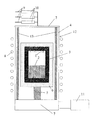
前記坩堝は、図2のように、真空排気容器内に設置されて、上記ガス雰囲気、圧力制御、及び温度制御される。前記真空排気容器は、通常、少なくとも、側壁となる二重石英管4、及び前記石英管の両端部(上下部)を閉じる蓋7で構成されている。
As shown in FIG. 2, the crucible is installed in an evacuated container, and the gas atmosphere, pressure control, and temperature control are performed. The evacuation vessel is usually composed of at least a
実際に上記改良レーリー法において結晶成長を行った場合、坩堝内部にセットしたSiC原料から発生した昇華ガスが坩堝の接合部を通過して坩堝の外に漏れ出し、さらに拡散して最終的には真空排気容器の内壁、例えば、二重石英管の内壁に付着して堆積する。前記堆積物は、前記内壁に膜状に形成される。この膜状の堆積物は、一回の成長のみでも相当な量が堆積するため、成長終了後に拭き取って除去しなければならない。特に、成長結晶の口径を大きくするほど、仕込むSiC原料の量も増加するため、一回の成長における前記堆積量も増加する。さらに、成長結晶の口径を大きくすると坩堝口径も大きくなるため、その結果として真空排気容器全体が大きくなり、特に、側壁を構成する二重石英管の内径がより大きくなって、成長後の内壁清掃作業の負担(作業時間等)はさらに増大する。 When crystal growth is actually performed in the improved Rayleigh method, the sublimation gas generated from the SiC raw material set inside the crucible leaks out of the crucible through the joint of the crucible, and further diffuses and finally It deposits on the inner wall of the vacuum evacuation vessel, for example, the inner wall of a double quartz tube. The deposit is formed in a film shape on the inner wall. Since a considerable amount of the film-like deposit is deposited only by one growth, it must be wiped off after the growth is completed. In particular, as the diameter of the grown crystal is increased, the amount of SiC raw material to be charged is increased, so that the amount of deposition in one growth is also increased. Furthermore, if the diameter of the growth crystal is increased, the diameter of the crucible is also increased. As a result, the entire vacuum evacuation vessel is increased. In particular, the inner diameter of the double quartz tube constituting the side wall is increased, and the inner wall is cleaned after the growth. The burden of work (work time, etc.) further increases.
そこで、本発明者らは、上記のようなSiC単結晶製造装置を発明し、真空排気容器の内壁(特に、二重石英管の内壁)に付着した堆積物の除去、清掃を効率良く迅速に行えるようにした。以下に、本発明のSiC単結晶製造装置の詳細を説明する。 Therefore, the present inventors invented the SiC single crystal manufacturing apparatus as described above, and efficiently and promptly removed and cleaned the deposits adhering to the inner wall of the vacuum exhaust container (particularly the inner wall of the double quartz tube). I was able to do it. Below, the detail of the SiC single crystal manufacturing apparatus of this invention is demonstrated.
本発明のSiC単結晶製造装置では、図3に示したように、真空排気容器12を形成する二重石英管4の内壁(内側)、及びこの二重石英管4の両端開口部分を塞ぐ2つの蓋7の内壁(内側)に剥離可能な粘着シート13を貼り付けている。剥離可能な粘着シート13を真空排気容器12の内壁に貼り付けることにより、坩堝3から漏れた昇華ガスが前記シート13の表面に付着して堆積し、真空排気容器12の内壁に直接付着するのを防止できる。成長終了後に、前記シート13を剥がすことにより、真空排気容器12内の堆積物を前記シート13とともに容易に除去できる。
In the SiC single crystal manufacturing apparatus of the present invention, as shown in FIG. 3, the inner wall (inside) of the
上記剥離可能な粘着シートは、真空排気容器の内壁に貼り付けてSiC単結晶を製造した後に、上述のように、剥がせるものである。人力で簡単に剥がせる程度の粘着力を有する粘着シートがより好ましく、シート基材に後述するような粘着剤からなる粘着層を備えたものが好適である。前記剥離可能な粘着シートにおけるシート基材の材質は、高周波をさえぎることのない電気絶縁性材料が好ましく(金属等の導電性材料では、高周波を遮断するので、坩堝の加熱を効率よく行えない)、かつ少なくとも200℃の耐熱性を有するのが好ましい。SiC単結晶成長中は、石英二重管の内部を冷却目的の水が循環しているため、石英二重管に貼られているシートの温度が200℃を越えることは無いため、シート基材の耐熱性は少なくとも200℃であればよい。前記耐熱性が、少なくとも250℃であると、剥離可能な粘着シートを繰り返し使用できる等でより好ましい。シート基材の具体的な材質としては、例えば、フッ素樹脂、ポリイミド樹脂、シリコーン樹脂等の耐熱樹脂を好適な例として挙げることができる。これらの耐熱樹脂には、粘土等の無機充填剤(無機粉末)や無機質繊維が混合されていてもよい。一方、粘着剤としては、ゴム系粘着剤、アクリル系粘着剤、ウレタン系粘着剤、シリコーン系粘着剤等を使用できるが、耐熱性を有するものがより好ましく、例えば、シリコーン系粘着剤が好適に使用できる。 The peelable pressure-sensitive adhesive sheet can be peeled off as described above after the SiC single crystal is produced by being attached to the inner wall of the vacuum exhaust container. A pressure-sensitive adhesive sheet having a pressure-sensitive adhesive force that can be easily peeled off by human power is more preferable, and a sheet base material provided with a pressure-sensitive adhesive layer made of a pressure-sensitive adhesive as described later is preferable. The material of the sheet base material in the peelable pressure-sensitive adhesive sheet is preferably an electrically insulating material that does not block high frequency (a conductive material such as metal blocks high frequency, so the crucible cannot be heated efficiently) And having a heat resistance of at least 200 ° C. During SiC single crystal growth, the water for cooling is circulated inside the quartz double tube, so the temperature of the sheet attached to the quartz double tube does not exceed 200 ° C. The heat resistance may be at least 200 ° C. It is more preferable that the heat resistance is at least 250 ° C. because a peelable adhesive sheet can be used repeatedly. As a specific material of the sheet substrate, for example, a heat resistant resin such as a fluororesin, a polyimide resin, and a silicone resin can be given as a suitable example. These heat-resistant resins may be mixed with an inorganic filler (inorganic powder) such as clay or inorganic fibers. On the other hand, as the pressure-sensitive adhesive, a rubber-based pressure-sensitive adhesive, an acrylic pressure-sensitive adhesive, a urethane-based pressure-sensitive adhesive, a silicone-based pressure-sensitive adhesive, and the like can be used, but those having heat resistance are more preferable. For example, a silicone-based pressure-sensitive adhesive is suitable. Can be used.
また、坩堝や坩堝を取り巻く断熱材の状態を常に目視観察できることが安全上も望ましいので、特に、真空排気容器を形成する二重石英管に貼る粘着シートは、石英管を通じてその内部や外部の観察ができる程度の透明性を有することがより望ましい。 In addition, it is desirable from the viewpoint of safety that the state of the crucible and the heat insulating material surrounding the crucible can always be visually observed. In particular, the adhesive sheet attached to the double quartz tube forming the evacuated container is observed inside and outside through the quartz tube It is more desirable to have transparency to such an extent that
前記再剥離粘着シートは、SiC単結晶成長が終了すると剥離されるものであるが、剥離したシートから堆積物を除去した後に再度真空排気容器の内壁に貼り付けて使用してもよい。その際に、粘着シートの粘着剤が、再接着できる粘着剤であることがより好ましい。再接着できる粘着剤の例としては、シリコーン系粘着剤が挙げられる。再接着できる粘着剤を有する粘着シートであれば、粘着剤を再度塗布することなく、複数回繰り返して使用できるので、SiC単結晶の製造コスト低減になるという有用な作用効果を奏する。 The re-peeling adhesive sheet is peeled off after the SiC single crystal growth is completed. However, after removing the deposit from the peeled sheet, it may be used again by being attached to the inner wall of the vacuum exhaust container. At that time, the pressure-sensitive adhesive of the pressure-sensitive adhesive sheet is more preferably a pressure-sensitive adhesive that can be reattached. Examples of the pressure-sensitive adhesive that can be re-adhered include a silicone-based pressure-sensitive adhesive. A pressure-sensitive adhesive sheet having a pressure-sensitive adhesive that can be re-adhered can be used repeatedly a plurality of times without re-applying the pressure-sensitive adhesive, and thus has a useful effect of reducing the production cost of the SiC single crystal.
また、本発明のSiC単結晶製造装置では、図4に示すように、真空排気容器の二重石英管にのみ粘着シートを貼り付けていても十分高い製造効率が得られる。真空排気容器の内壁のうち、二重石英管の占める面積が大きいこと(堆積物の除去作業の大半が二重石英管の除去となる)、また、真空排気容器内外の視認性を確保する必要があることから、真空排気容器の内壁に剥離可能な粘着シートを貼るのみであっても、十分上記効果が得られるものである。 In the SiC single crystal manufacturing apparatus of the present invention, as shown in FIG. 4, sufficiently high manufacturing efficiency can be obtained even if an adhesive sheet is attached only to the double quartz tube of the vacuum exhaust container. Of the inner wall of the vacuum evacuation vessel, the area occupied by the double quartz tube is large (most of the deposit removal work is removal of the double quartz tube), and it is necessary to ensure visibility inside and outside the vacuum evacuation vessel Therefore, even if only a peelable adhesive sheet is attached to the inner wall of the vacuum exhaust container, the above effect can be obtained sufficiently.
本発明では、真空排気容器の内壁に剥離可能な粘着シートを2層以上の複数層にして重ねて貼り付けるようにしてもよい。複数層(複数枚)重ねて貼り付けられていると、SiC単結晶成長が終了して、貼り付けられた前記シートの上層一枚を剥がすと下層の新しい粘着シートが現れるので、次のSiC単結晶成長を行うに当たり、粘着シートを貼り付ける作業を省略できる。すなわち、製造効率がより高くなる。重ねて貼り付ける層の数の上限は、特に限定するものではないが、20層を超えると、貼り付けた総厚さが大きくなり過ぎて好ましくない場合が出てくる。 In the present invention, a peelable adhesive sheet may be laminated on the inner wall of the vacuum evacuation container in a plurality of layers and pasted together. When multiple layers (multiple sheets) are laminated and pasted, the SiC single crystal growth is completed, and when the upper layer of the pasted sheet is peeled off, a new adhesive sheet in the lower layer appears. In performing crystal growth, the work of attaching an adhesive sheet can be omitted. That is, the production efficiency becomes higher. The upper limit of the number of layers to be laminated is not particularly limited. However, if the number exceeds 20 layers, the total thickness of the pasted layers may become too large, which may be undesirable.
以下に、本発明の実施例について述べる。
(実施例1)
図3に示すSiC単結晶成長装置を用いて、SiC単結晶を製造する例について説明する。SiC結晶成長は、SiC粉末2を昇華させ、種結晶として用いたSiC単結晶1上で再結晶化させることにより行われる。種結晶のSiC単結晶1は、黒鉛製坩堝3の内部の上面(蓋体内側)に取り付けられる。原料のSiC粉末2は、黒鉛製坩堝3の内部の下方に充填されている。このような黒鉛製坩堝3は、真空排気容器12の内部に、黒鉛の支持棒5により設置される。黒鉛製坩堝の周囲には、熱シールドのための黒鉛製断熱材6が設置されている。真空排気容器12は、真空排気装置11により高真空排気(10-3Pa以下)することができ、かつ、内部雰囲気を、ガス配管9及びガス流量調節計10を通って導入されるArガスにより圧力制御することができる。各種ド−ピングガス(窒素、トリメチルアルミニウム、トリメチルボロン)も、ガス流量調節計10を通して導入することができる。また、真空排気容器12の側壁を構成する二重石英管4の外周には、ワークコイル8が設置されており、高周波電流を流すことにより黒鉛製坩堝を加熱し、原料及び種結晶を加熱することができる。坩堝温度の計測は、坩堝下部を覆う断熱材の中央部に直径2〜4mmの光路を設け坩堝上部及び下部からの光を取り出し、二色温度計を用いて行う。
Examples of the present invention will be described below.
Example 1
An example of manufacturing a SiC single crystal using the SiC single crystal growth apparatus shown in FIG. 3 will be described. The SiC crystal growth is performed by sublimating the
以下、本発明のSiC単結晶成長装置を用いた具体的な結晶成長の例を説明する。
先ず、種結晶1として、口径50mmの(0001)面を有した4HポリタイプのSiC単結晶ウェハを用意した。次に、種結晶1を黒鉛製坩堝3の内部、上面に取り付けた。黒鉛製坩堝3の内部には、アチソン法により作製したSiC結晶原料粉末2を充填した。次いで、黒鉛製坩堝容器3を黒鉛製フェルト6で被覆した後、黒鉛製支持棒5の上に載せ、真空排気容器12の内部に設置した。その後、図3に示すように、真空排気容器12の二重石英管4の内面(内壁)全体を被覆するように、剥離可能な粘着シート13(ウノン技研製K-1000A、耐熱温度:260℃、シート基材:ポリイミド樹脂、粘着剤:耐熱アクリル粘着剤、厚さ:100μm)を貼り付けた。なお、真空排気容器12を構成する二重石英管4のサイズは、30cm径×1m長さである。
Hereinafter, a specific example of crystal growth using the SiC single crystal growth apparatus of the present invention will be described.
First, as a seed crystal 1, a 4H polytype SiC single crystal wafer having a (0001) plane with a diameter of 50 mm was prepared. Next, the seed crystal 1 was attached to the inside and upper surface of the
そして、真空排気容器12の内部を真空排気装置11で真空排気した後、ワークコイルに電流を流し、原料温度を2000℃まで上げた。その後、雰囲気ガスとして高純度Arガス(純度99.9995%)を流入させ、真空排気容器12内の圧力は成長全体を通じて1.3kPaに保った。この圧力下において、原料温度を2000℃から目標温度である2400℃まで上昇させ、その後、同温度を保って45時間成長を続けた。この成長時間中、窒素流量を0.5×10⁻⁶m3/sec(同流量にて、成長結晶中の窒素濃度が1×1019cm-3となる)とし、成長終了時まで保った。
And after evacuating the inside of the
成長後、真空排気容器12内を大気開放して坩堝3を取り出した後、二重石英管4の内面の粘着シート13を観察したところ、昇華ガスの坩堝からのリークにより、坩堝上面に近い位置に貼られた粘着シート13の表面を最大規模として、広い面積に渡って堆積物が膜状に付着していた。ここで、粘着シート13を剥がして全面取り外すことで、堆積物が付着したシート13を回収した。二重石英管4の内側には、シート13を剥がす際に若干の堆積物が落ちたが、吸引等で容易に除去できるものであった。
After the growth, the
次のSiC成長準備には、新たに剥離可能な粘着シート13を再び二重石英管4内面全体を被覆するように、貼り付けた。この一連の作業は、5分間という短時間で全て完了でき、非常に効率の良い作業で次回成長を開始できた。
For the next SiC growth preparation, a newly peelable pressure-
(実施例2)
実施例1と同様の手順で、SiC単結晶を成長させた。但し、図3に示したように、真空排気容器12の内壁(二重石英管7の内壁、及びその上下蓋7の内面)に剥離可能な粘着シート13(日東電工製TRM3650S、耐熱温度:260℃、シート基材:ポリイミド樹脂、粘着剤:シリコーン粘着剤、厚さ:31μm)を貼り付けた。
(Example 2)
A SiC single crystal was grown in the same procedure as in Example 1. However, as shown in FIG. 3, an adhesive sheet 13 (TRM3650S manufactured by Nitto Denko, heat resistant temperature: 260) that can be peeled off from the inner wall of the vacuum exhaust vessel 12 (the inner wall of the
実施例1と同様に成長を行い、成長終了後、真空排気容器12内を大気開放して坩堝3を取り出した後、真空排気容器12の内壁の粘着シート13を観察したところ、昇華ガスの坩堝からのリークにより、坩堝上面に近い位置に貼られた粘着シート13の表面を最大規模として、広い面積に渡って堆積物が膜状に付着していた。ここで、粘着シート13を剥がして全面取り外すことで、堆積物が付着したシートを回収した。真空排気容器12の内部には、シート13を剥がす際に若干の堆積物が落ちたが、吸引等で容易に除去できるものであった。本実施例では、真空排気容器12の上下蓋7の内壁へ付着した堆積物も容易に除去できるものであった。
Growth was performed in the same manner as in Example 1. After the growth was completed, the inside of the
次のSiC成長準備には、新たに剥離可能な粘着シート13を再び真空排気容器12の内壁に、図3のように貼り付けた。この一連の作業は、8分間という短時間で全て完了でき、非常に効率の良い作業で次回成長を開始できた。
For the next SiC growth preparation, a newly peelable
(実施例3)
実施例1と同様の手順で、SiC単結晶を成長させた。但し、二重石英管4の内壁に貼り付けた剥離可能な粘着シート13(TACONIC社製特殊高耐熱性シリコーン粘着テープTacsil F20、耐熱温度:260℃、シート基材:フッ素樹脂+ガラスクロス、ポリイミドフィルム 粘着剤:シリコーン粘着剤、厚さ:200μm)は、再接着できる粘着剤を使用したものである。
(Example 3)
A SiC single crystal was grown in the same procedure as in Example 1. However, the
成長後、真空排気容器12内を大気開放して坩堝を取り出した後、二重石英管4の内面の粘着シート7を観察したところ、昇華ガスの坩堝からのリークにより、坩堝上面に近い位置に貼られた粘着シート13の表面を最大規模として、広い面積に渡って堆積物が膜状に付着していた。ここで、粘着シート13を剥がして全面取り外すことで、堆積物が付着したシートを回収した。二重石英管4の内側には、前記シート13を剥がす際に若干の堆積物が落ちたが、吸引等で容易に除去できるものであった。また、堆積物が付着したシート13の堆積物を除去した後、次のSiC成長の際に、同シートを貼り付けて使用した。
After the growth, the inside of the evacuated
次のSiC成長準備には、一度使用した後の粘着シート13を再び二重石英管4内面全体を被覆するように、貼り付けた。成長後の状況は、前記と同じであり、二重石英管4の清掃は容易にできた。
In preparation for the next SiC growth, the
(実施例4)
実施例1と同様の手順で、SiC単結晶を成長させた。但し、二重石英管4の内壁に貼り付けた剥離可能な粘着シート13(TACONIC社製特殊高耐熱性シリコーン粘着テープTacsil F20、耐熱温度:260℃、シート基材:フッ素樹脂+ガラスクロス、ポリイミドフィルム 粘着剤:シリコーン粘着剤、厚さ:200μm)は、5層に重ねて貼り付けた。
Example 4
A SiC single crystal was grown in the same procedure as in Example 1. However, the
成長後、真空排気容器12内を大気開放して坩堝を取り出した後、二重石英管4の内面の粘着シート13を観察したところ、昇華ガスの坩堝からのリークにより、坩堝上面に近い位置に貼られた粘着シート13の表面を最大規模として、広い面積に渡って堆積物が膜状に付着していた。ここで、粘着シート13を剥がして全面取り外すことで、堆積物が付着したシートを回収した。二重石英管4の内側には、シート13を剥がす際に若干の堆積物が落ちたが、吸引等で容易に除去できるものであった。
After the growth, after the
次のSiC成長準備には、堆積物が付着した粘着シートを剥がしても下層の粘着シート13が現れるので、粘着シートを貼り付ける作業を省略でき、そのまま次のSiC成長を開始できた。
In preparation for the next SiC growth, even if the pressure-sensitive adhesive sheet to which the deposit was attached was peeled off, the lower-layer pressure-
(比較例1)
真空排気容器12の内壁に剥離可能な粘着シート13を貼り付けることを実施しなかった以外は全て実施例1と同様にして結晶成長を行った。
(Comparative Example 1)
Crystal growth was performed in the same manner as in Example 1 except that the
成長後、真空排気容器12内を大気開放して坩堝を取り出した後、真空排気容器の内壁、特に二重石英管内面を観察したところ、昇華ガスの坩堝からのリークにより、内面の坩堝上面に近い位置を最大規模として、広い面積に渡って堆積物が膜状に付着していた。ここで前記堆積物を取り除くために、二重石英管4内面に付着していた堆積物を手作業で拭き取った。この作業には1時間以上の時間を要し、さらに堆積物が剥がれ落ちて生ずる粉体も大量に発生し、吸引掃除機で完全に吸い取るのにも20分程度の時間を要した。その結果として、作業全体で1時間20分以上の時間を要し、次のSiC成長準備は、上記実施例に比べて長時間を要するもので極めて製造効率の悪いものであった。前記手順で、SiC単結晶の製造を繰り返し行うと、完全に除去されていない堆積物が隅部等に蓄積し、真空排気容器の寿命が、前記実施例に比べて半減するものであった。
After the growth, the inside of the
また、前記堆積物を除去しないで、次のSiC単結晶の製造を行うと、Oリング等に付着した堆積物によって真空漏れが生じて結晶成長を中止しなければならなくなった。 Further, when the next SiC single crystal was manufactured without removing the deposit, a vacuum leak occurred due to the deposit adhering to the O-ring or the like, and the crystal growth had to be stopped.
1 種結晶(SiC単結晶)
2 SiC結晶粉末原料
3 坩堝容器(黒鉛あるいはタンタル等の高融点金属)
4 二重石英管
5 支持棒
6 黒鉛製フェルト(断熱材)
7 二重石英管の蓋
8 ワークコイル
9 ガス配管
10 ガス用マスフローコントローラ
11 真空排気装置
12 真空排気容器
13 剥離可能な粘着シート
1 Seed crystal (SiC single crystal)
2 Raw material for
4
7 Cover of
Claims (3)
Priority Applications (1)
| Application Number | Priority Date | Filing Date | Title |
|---|---|---|---|
| JP2009177412A JP5146423B2 (en) | 2009-07-30 | 2009-07-30 | Silicon carbide single crystal manufacturing equipment |
Applications Claiming Priority (1)
| Application Number | Priority Date | Filing Date | Title |
|---|---|---|---|
| JP2009177412A JP5146423B2 (en) | 2009-07-30 | 2009-07-30 | Silicon carbide single crystal manufacturing equipment |
Publications (2)
| Publication Number | Publication Date |
|---|---|
| JP2011032109A JP2011032109A (en) | 2011-02-17 |
| JP5146423B2 true JP5146423B2 (en) | 2013-02-20 |
Family
ID=43761559
Family Applications (1)
| Application Number | Title | Priority Date | Filing Date |
|---|---|---|---|
| JP2009177412A Active JP5146423B2 (en) | 2009-07-30 | 2009-07-30 | Silicon carbide single crystal manufacturing equipment |
Country Status (1)
| Country | Link |
|---|---|
| JP (1) | JP5146423B2 (en) |
Cited By (2)
| Publication number | Priority date | Publication date | Assignee | Title |
|---|---|---|---|---|
| US9532727B2 (en) | 2008-06-06 | 2017-01-03 | Koninklijke Philips N.V. | Method and apparatus for illuminating the interior of a medical imaging device |
| US10597226B2 (en) | 2017-02-16 | 2020-03-24 | Fanuc Corporation | Float and evaporation suppressing method |
Families Citing this family (2)
| Publication number | Priority date | Publication date | Assignee | Title |
|---|---|---|---|---|
| JP6029492B2 (en) * | 2013-02-26 | 2016-11-24 | 信越半導体株式会社 | Method for producing silicon carbide |
| CN114877680B (en) * | 2022-05-13 | 2023-09-22 | 连城凯克斯科技有限公司 | Gas conversion device for silicon carbide vertical induction synthesis furnace |
Family Cites Families (3)
| Publication number | Priority date | Publication date | Assignee | Title |
|---|---|---|---|---|
| JPH0233049Y2 (en) * | 1985-11-12 | 1990-09-06 | ||
| JP2007157923A (en) * | 2005-12-02 | 2007-06-21 | Nitto Denko Corp | Processing chamber and its protective material |
| JP2008074653A (en) * | 2006-09-20 | 2008-04-03 | Bridgestone Corp | Apparatus for producing silicon carbide single crystal |
-
2009
- 2009-07-30 JP JP2009177412A patent/JP5146423B2/en active Active
Cited By (2)
| Publication number | Priority date | Publication date | Assignee | Title |
|---|---|---|---|---|
| US9532727B2 (en) | 2008-06-06 | 2017-01-03 | Koninklijke Philips N.V. | Method and apparatus for illuminating the interior of a medical imaging device |
| US10597226B2 (en) | 2017-02-16 | 2020-03-24 | Fanuc Corporation | Float and evaporation suppressing method |
Also Published As
| Publication number | Publication date |
|---|---|
| JP2011032109A (en) | 2011-02-17 |
Similar Documents
| Publication | Publication Date | Title |
|---|---|---|
| JP5483216B2 (en) | SiC single crystal and method for producing the same | |
| WO2010024390A1 (en) | METHOD AND APPARATUS FOR MANUFACTURING SiC SINGLE CRYSTAL FILM | |
| JP2012036088A (en) | Method and apparatus for growing low defect density silicon carbide and resulting material | |
| CN110904509B (en) | Silicon carbide crystal, method and apparatus for growing the same, semiconductor device, and display device | |
| JP5526866B2 (en) | Silicon carbide crystal manufacturing method and silicon carbide crystal manufacturing apparatus | |
| WO2000039372A1 (en) | Method for growing single crystal of silicon carbide | |
| US20160307800A1 (en) | Method for manufacturing a silicon carbide wafer and respective equipment | |
| JP2007230823A (en) | Method for manufacturing silicon carbide single crystal ingot, and silicon carbide single crystal ingot | |
| JP4523733B2 (en) | Method for producing silicon carbide single crystal ingot and method for mounting seed crystal for growing silicon carbide single crystal | |
| JP5146423B2 (en) | Silicon carbide single crystal manufacturing equipment | |
| JP2008110907A (en) | Method for producing silicon carbide single crystal ingot, and silicon carbide single crystal ingot | |
| JP4733882B2 (en) | Silicon carbide single crystal, method for producing the same, and silicon carbide crystal raw material for growing silicon carbide single crystal | |
| JP4253974B2 (en) | SiC single crystal and growth method thereof | |
| JP2005239496A (en) | Silicon carbide raw material for growing silicon carbide single crystal, silicon carbide single crystal, and method for producing the same | |
| EP1233085B1 (en) | SiC SINGLE CRYSTAL AND METHOD FOR GROWING THE SAME | |
| JP5761264B2 (en) | Method for manufacturing SiC substrate | |
| JP5948988B2 (en) | Method for producing silicon carbide single crystal | |
| JP5333363B2 (en) | Silicon carbide raw material for growing silicon carbide single crystal and method for producing silicon carbide single crystal using the same | |
| Wang et al. | Study on carbon particle inclusions during 4H-SiC growth by using physical vapor transport system | |
| JP2009102187A (en) | Crucible for growth of silicon carbide single crystal, method of manufacturing silicon carbide single crystal using the same, and silicon carbide single crystal ingot | |
| JP2011201755A (en) | Method for producing single crystal silicon carbide | |
| JP6594238B2 (en) | Silicon carbide single crystal manufacturing equipment | |
| JP2013006739A (en) | Method for producing single crystal | |
| JP2003137694A (en) | Seed crystal for growing silicon carbide single crystal, silicon carbide single crystal ingot and method of producing the same | |
| JP2002293694A (en) | Silicon carbide single crystal ingot and method of manufacturing for the same |
Legal Events
| Date | Code | Title | Description |
|---|---|---|---|
| A621 | Written request for application examination |
Free format text: JAPANESE INTERMEDIATE CODE: A621 Effective date: 20110816 |
|
| A977 | Report on retrieval |
Free format text: JAPANESE INTERMEDIATE CODE: A971007 Effective date: 20120720 |
|
| A131 | Notification of reasons for refusal |
Free format text: JAPANESE INTERMEDIATE CODE: A131 Effective date: 20120807 |
|
| A521 | Request for written amendment filed |
Free format text: JAPANESE INTERMEDIATE CODE: A523 Effective date: 20120927 |
|
| TRDD | Decision of grant or rejection written | ||
| A01 | Written decision to grant a patent or to grant a registration (utility model) |
Free format text: JAPANESE INTERMEDIATE CODE: A01 Effective date: 20121030 |
|
| A61 | First payment of annual fees (during grant procedure) |
Free format text: JAPANESE INTERMEDIATE CODE: A61 Effective date: 20121112 |
|
| R151 | Written notification of patent or utility model registration |
Ref document number: 5146423 Country of ref document: JP Free format text: JAPANESE INTERMEDIATE CODE: R151 |
|
| FPAY | Renewal fee payment (event date is renewal date of database) |
Free format text: PAYMENT UNTIL: 20151207 Year of fee payment: 3 |
|
| S111 | Request for change of ownership or part of ownership |
Free format text: JAPANESE INTERMEDIATE CODE: R313113 |
|
| R350 | Written notification of registration of transfer |
Free format text: JAPANESE INTERMEDIATE CODE: R350 |
|
| S111 | Request for change of ownership or part of ownership |
Free format text: JAPANESE INTERMEDIATE CODE: R313111 |
|
| R350 | Written notification of registration of transfer |
Free format text: JAPANESE INTERMEDIATE CODE: R350 |
|
| S531 | Written request for registration of change of domicile |
Free format text: JAPANESE INTERMEDIATE CODE: R313531 |
|
| R350 | Written notification of registration of transfer |
Free format text: JAPANESE INTERMEDIATE CODE: R350 |