JP5145984B2 - Semiconductor manufacturing apparatus and semiconductor device manufacturing method using the same - Google Patents
Semiconductor manufacturing apparatus and semiconductor device manufacturing method using the same Download PDFInfo
- Publication number
- JP5145984B2 JP5145984B2 JP2008024843A JP2008024843A JP5145984B2 JP 5145984 B2 JP5145984 B2 JP 5145984B2 JP 2008024843 A JP2008024843 A JP 2008024843A JP 2008024843 A JP2008024843 A JP 2008024843A JP 5145984 B2 JP5145984 B2 JP 5145984B2
- Authority
- JP
- Japan
- Prior art keywords
- susceptor
- main shaft
- semiconductor wafer
- semiconductor
- arm
- Prior art date
- Legal status (The legal status is an assumption and is not a legal conclusion. Google has not performed a legal analysis and makes no representation as to the accuracy of the status listed.)
- Active
Links
- 239000004065 semiconductor Substances 0.000 title claims description 236
- 238000004519 manufacturing process Methods 0.000 title claims description 39
- 235000012431 wafers Nutrition 0.000 claims description 198
- 229910052736 halogen Inorganic materials 0.000 claims description 70
- 150000002367 halogens Chemical class 0.000 claims description 68
- 238000010438 heat treatment Methods 0.000 claims description 11
- 239000012495 reaction gas Substances 0.000 claims 1
- 239000010453 quartz Substances 0.000 description 11
- VYPSYNLAJGMNEJ-UHFFFAOYSA-N silicon dioxide Inorganic materials O=[Si]=O VYPSYNLAJGMNEJ-UHFFFAOYSA-N 0.000 description 11
- 230000002093 peripheral effect Effects 0.000 description 10
- 238000001816 cooling Methods 0.000 description 7
- 230000015572 biosynthetic process Effects 0.000 description 3
- 239000000498 cooling water Substances 0.000 description 2
- 230000000694 effects Effects 0.000 description 2
- 125000005843 halogen group Chemical group 0.000 description 2
- 239000012535 impurity Substances 0.000 description 2
- 230000001105 regulatory effect Effects 0.000 description 2
- 238000002791 soaking Methods 0.000 description 2
- 238000007796 conventional method Methods 0.000 description 1
- MROCJMGDEKINLD-UHFFFAOYSA-N dichlorosilane Chemical compound Cl[SiH2]Cl MROCJMGDEKINLD-UHFFFAOYSA-N 0.000 description 1
- 238000002347 injection Methods 0.000 description 1
- 239000007924 injection Substances 0.000 description 1
- 238000000034 method Methods 0.000 description 1
Images


Description
本発明は、半導体ウエハに熱処理を行うための半導体製造装置およびそれを用いた半導体装置の製造方法に関する。 The present invention relates to a semiconductor manufacturing apparatus for performing a heat treatment on a semiconductor wafer and a manufacturing method of a semiconductor device using the same.
従来より、サセプタおよびサセプタ支持シャフトを備えた半導体製造装置が、例えば特許文献1で提案されている。具体的に、特許文献1では、メインシャフトおよびこのメインシャフトから放射状に延びる3本のアームから構成されたサセプタ支持シャフトと、一面に一枚の半導体ウエハが配置され、他面にサセプタ支持シャフトの各アームが接続されるサセプタとを備えた枚葉式の半導体製造装置が提案されている。アームは、サセプタの他面の周縁部に接続されている。また、サセプタは処理チャンバ内に配置され、処理チャンバの外部に配置されたハロゲンランプによって加熱されるようになっている。 Conventionally, a semiconductor manufacturing apparatus including a susceptor and a susceptor support shaft has been proposed in Patent Document 1, for example. Specifically, in Patent Document 1, a susceptor support shaft composed of a main shaft and three arms extending radially from the main shaft, a semiconductor wafer on one surface, and a susceptor support shaft on the other surface are arranged. A single wafer type semiconductor manufacturing apparatus including a susceptor to which each arm is connected has been proposed. The arm is connected to the peripheral edge of the other surface of the susceptor. The susceptor is disposed in the processing chamber and heated by a halogen lamp disposed outside the processing chamber.
このような装置では、サセプタの他面の中心部にサセプタ支持シャフトの突起部が配置されないため、処理チャンバの下部側に配置されたハロゲンランプの輻射熱がサセプタ中心部においてサセプタ支持シャフトによって妨げられないようになっている。
しかしながら、上記従来の技術では、サセプタ上の1枚の半導体ウエハを均熱化することはできるが、サセプタに複数の半導体ウエハを配置することにより、以下の問題が生じることが発明者らの検討により明らかになった。 However, in the above conventional technique, although one semiconductor wafer on the susceptor can be soaked, the following problems arise when the plurality of semiconductor wafers are arranged on the susceptor. It became clear.
まず、サセプタの一面に複数の半導体ウエハを配置し、サセプタ下部のハロゲンランプからサセプタの他面に光を照射すると、サセプタの他面にアームの影ができてしまう。サセプタを回転させたとしても、アームはサセプタと共に回転することから、サセプタの他面に常にアームの影ができてしまう。したがって、サセプタの一面においてアームの影に対応する場所に配置された半導体ウエハのうち影の影響で温度が上がらない部分の膜厚が薄くなるという問題がある。 First, when a plurality of semiconductor wafers are arranged on one surface of a susceptor and light is irradiated on the other surface of the susceptor from a halogen lamp below the susceptor, an arm shadow is formed on the other surface of the susceptor. Even if the susceptor is rotated, the arm rotates with the susceptor, so that the shadow of the arm is always formed on the other surface of the susceptor. Therefore, there is a problem that the film thickness of the portion of the semiconductor wafer arranged on the one surface of the susceptor corresponding to the shadow of the arm is not increased due to the influence of the shadow.
また、処理チャンバ内に一方向に成膜ガスを流すことにより、サセプタから処理チャンバ側への熱の逃げがあるため、アームをサセプタの周縁部に接続するということは、アームを介してサセプタの熱をメインシャフト側に逃がすことにもなる。これにより、半導体ウエハの外径方向に熱分布が形成されると共に、サセプタのうちアームが接続された場所の周辺の熱がアーム側に逃げるために半導体ウエハの周方向に熱分布が形成され、膜厚の不均一化が生じてしまうという問題がある。 In addition, since a film forming gas flows in one direction in the processing chamber, there is a heat escape from the susceptor to the processing chamber side. Therefore, connecting the arm to the peripheral portion of the susceptor means that the susceptor is connected via the arm. Heat will also escape to the main shaft. Thereby, a heat distribution is formed in the outer diameter direction of the semiconductor wafer, and a heat distribution in the circumferential direction of the semiconductor wafer is formed in order to escape the heat around the susceptor where the arm is connected to the arm side, There is a problem that the film thickness becomes non-uniform.
さらに、近年の半導体ウエハの大型化により、サセプタと半導体ウエハとを合わせた重量が大きくなると、サセプタを支持するアームを太くするか、あるいはアームの本数を増加させる必要がある。これにより、アームを介した熱の逃げが大きくなることや、サセプタの他面に現れるアームの影が増加するため、サセプタの温度が下がり、成膜に影響が生じるという問題がある。 Furthermore, when the combined weight of the susceptor and the semiconductor wafer increases due to the recent increase in the size of the semiconductor wafer, it is necessary to increase the number of arms that support the susceptor or to increase the number of arms. Accordingly, there is a problem that heat escape through the arm is increased and the shadow of the arm appearing on the other surface of the susceptor is increased, so that the temperature of the susceptor is lowered and film formation is affected.
本発明は、上記点に鑑み、サセプタに複数の半導体ウエハを配置して熱処理するに際し、各半導体ウエハの均熱化を図ることができる半導体製造装置およびそれを用いた半導体装置の製造方法を提供することを目的とする。 SUMMARY OF THE INVENTION In view of the above, the present invention provides a semiconductor manufacturing apparatus and a method of manufacturing a semiconductor device using the same, in which a plurality of semiconductor wafers are placed on a susceptor and heat-treated when the semiconductor wafers are heat-treated. The purpose is to do.
上記目的を達成するため、請求項1に記載の発明では、処理チャンバ(10)内に配置され、一面(21)および他面(22)を有し、一面(21)に複数の半導体ウエハ(60)が配置されるサセプタ(20)と、サセプタ(20)の他面(22)側に位置すると共に、サセプタ(20)の他面(22)に対し垂直方向に延びる棒状のメインシャフト(31)と、該メインシャフト(31)のうち前記サセプタ(20)側の上端部(31a)から放射状に延びてサセプタ(20)の他面(22)に接続される複数のアーム(32)とを有するシャフト(30)と、サセプタ(20)の他面(22)側であって、処理チャンバ(10)の外部に配置され、加熱源となるハロゲンランプ(40)とを有する半導体製造装置であって、サセプタ(20)の一面(21)に垂直な方向で、メインシャフト(31)の上端部(31a)および各アーム(32)と半導体ウエハ(60)とが離間していると共に、各アーム(32)の間に半導体ウエハ(60)が配置されていることを特徴とする。 In order to achieve the above object, according to the invention described in claim 1, the semiconductor wafer is disposed in the processing chamber (10), has one surface (21) and the other surface (22), and a plurality of semiconductor wafers ( 60) on which the susceptor (20) is disposed, and a rod-shaped main shaft (31) which is located on the other surface (22) side of the susceptor (20) and extends in a direction perpendicular to the other surface (22) of the susceptor (20). ) And a plurality of arms (32) extending radially from the upper end (31a) on the susceptor (20) side of the main shaft (31) and connected to the other surface (22) of the susceptor (20). This is a semiconductor manufacturing apparatus having a shaft (30) having a halogen lamp (40) which is disposed outside the processing chamber (10) on the other surface (22) side of the susceptor (20) and serves as a heating source. Susceptor ( 0) in the direction perpendicular to the one surface (21), the upper end portion (31a) of the main shaft (31) and the arms (32) are separated from the semiconductor wafer (60), and the arms (32) A semiconductor wafer (60) is disposed therebetween.
これによると、各半導体ウエハ(60)がアーム(32)の影にならないようにすることができる。すなわち、アーム(32)がハロゲンランプ(40)の輻射熱を阻害しないようにすることができるので、各半導体ウエハ(60)をそれぞれ均一に加熱することができ、半導体ウエハ(60)内での膜厚の均一化を図ることができる。
また、半導体ウエハ(60)の成膜における膜厚制御や不純物濃度の制御性を向上させることができる。さらに、半導体ウエハ(60)の温度が不均一になることで半導体ウエハ(60)に応力が生じるスリップ発生を防止することができる。
According to this, each semiconductor wafer (60) can be prevented from being shaded by the arm (32). That is, since the arm (32) can be prevented from hindering the radiant heat of the halogen lamp (40), each semiconductor wafer (60) can be heated uniformly, and the film in the semiconductor wafer (60) can be heated. The thickness can be made uniform.
In addition, film thickness control and impurity concentration controllability in the film formation of the semiconductor wafer (60) can be improved. Furthermore, it is possible to prevent the occurrence of slip that causes stress in the semiconductor wafer (60) due to the non-uniform temperature of the semiconductor wafer (60).
請求項2に記載の発明では、メインシャフト(31)のうち上端部(31a)とは反対側の下端部(31b)に回転機構(50)を有し、回転機構(50)によってメインシャフト(31)の中心軸を中心にサセプタ(20)が回転させられるようになっていることを特徴とする。 In the invention according to claim 2, the main shaft (31) has the rotation mechanism (50) at the lower end (31b) opposite to the upper end (31a), and the rotation mechanism (50) causes the main shaft ( The susceptor (20) can be rotated around the central axis of 31).
これにより、サセプタ(20)の周方向に対し、ハロゲンランプ(40)の配置位置のばらつきやハロゲンランプ(40)の照度のばらつきがある場合にも、サセプタ(20)が回転することにより、半導体ウエハ(60)においてサセプタ(20)の周方向の温度分布を無くすことができる。 As a result, the susceptor (20) rotates and the semiconductor is rotated even when there is a variation in the arrangement position of the halogen lamp (40) and a variation in the illuminance of the halogen lamp (40) with respect to the circumferential direction of the susceptor (20). The temperature distribution in the circumferential direction of the susceptor (20) in the wafer (60) can be eliminated.
請求項3に記載の発明では、サセプタ(20)の一面(21)に配置される半導体ウエハ(60)の数と、アーム(32)の数とは同じであることを特徴とする。 The invention according to claim 3 is characterized in that the number of semiconductor wafers (60) arranged on one surface (21) of the susceptor (20) and the number of arms (32) are the same.
これによると、各半導体ウエハ(60)がアーム(32)の影にならないようにすることができる。すなわち、アーム(32)がハロゲンランプ(40)の輻射熱を阻害しないようにすることができるので、各半導体ウエハ(60)をそれぞれ均一に加熱することができ、半導体ウエハ(60)内での膜厚の均一化を図ることができる。アーム(32)の数を半導体ウエハ(60)の数と同じ本数とすることにより輻射熱を阻害しないで保持するアーム(32)の本数を最大にすることができるため、一本あたりのアーム(32)にかかるサセプタ(20)の荷重を小さくすることができるため、アーム(32)の太さを小さくできる。そのため、アーム(32)がサセプタ(20)を保持する部分からの熱の逃げを小さくできるためより均熱をはかることができる。 According to this, each semiconductor wafer (60) can be prevented from being shaded by the arm (32). That is, since the arm (32) can be prevented from hindering the radiant heat of the halogen lamp (40), each semiconductor wafer (60) can be heated uniformly, and the film in the semiconductor wafer (60) can be heated. The thickness can be made uniform. By setting the number of arms (32) to be the same as the number of semiconductor wafers (60), the number of arms (32) to be held without hindering radiant heat can be maximized. ) Can reduce the load of the susceptor (20), so that the thickness of the arm (32) can be reduced. Therefore, since the escape of heat from the portion where the arm (32) holds the susceptor (20) can be reduced, soaking can be further achieved.
請求項4に記載の発明では、サセプタ(20)の他面(22)側に配置されるハロゲンランプ(40)の数と、サセプタ(20)の一面(21)に配置される半導体ウエハ(60)の数と、アーム(32)の数とは同じであることを特徴とする。 In the invention according to claim 4, the number of halogen lamps (40) arranged on the other surface (22) side of the susceptor (20) and the semiconductor wafer (60) arranged on one surface (21) of the susceptor (20). ) And the number of arms (32) are the same.
これにより、アーム(32)の影ができるサセプタ(20)の他面(22)側において、半導体ウエハ(60)とアーム(32)とハロゲンランプ(40)との関係を全ての半導体ウエハ(60)に対して対称にすることができるため、全ての半導体ウエハ(60)を均一に熱処理することができる。 Thereby, on the other surface (22) side of the susceptor (20) where the shadow of the arm (32) can be formed, the relationship among the semiconductor wafer (60), the arm (32), and the halogen lamp (40) is determined for all the semiconductor wafers (60). ), All semiconductor wafers (60) can be uniformly heat-treated.
請求項5に記載の発明では、サセプタ(20)の他面(22)とアーム(32)との接続点(23)が、半導体ウエハ(60)のうちメインシャフト(31)の中心軸からもっとも離れた位置よりもメインシャフト(31)の中心軸側に位置していることを特徴とする。 In the invention according to claim 5, the connection point (23) between the other surface (22) of the susceptor (20) and the arm (32) is most distant from the central axis of the main shaft (31) of the semiconductor wafer (60). It is characterized by being located closer to the central axis of the main shaft (31) than the distant position.
これにより、処理チャンバ(10)側への熱の逃げが大きいサセプタ(20)の外周部から離れた場所にアーム(32)の接続点(23)を設けることができる。したがって、サセプタ(20)の外周側への新たな熱の逃げの経路を作らないようにすることができ、半導体ウエハ(60)の均熱化を図ることができる。 Thereby, the connection point (23) of an arm (32) can be provided in the place away from the outer peripheral part of the susceptor (20) with large escape of heat to the processing chamber (10) side. Therefore, it is possible not to create a new heat escape path to the outer peripheral side of the susceptor (20), and to equalize the temperature of the semiconductor wafer (60).
請求項6に記載の発明では、サセプタ(20)の一面(21)の面方向において、半導体ウエハ(60)の側面とサセプタ(20)の側面との最短距離をbとし、半導体ウエハ(60)の側面と接続点(23)との最短距離をcとしたとき、c>bの条件を満たすことを特徴とする。 In the invention according to claim 6, in the surface direction of the one surface (21) of the susceptor (20), the shortest distance between the side surface of the semiconductor wafer (60) and the side surface of the susceptor (20) is b, and the semiconductor wafer (60). When the shortest distance between the side surface and the connection point (23) is c, the condition of c> b is satisfied.
これにより、サセプタ(20)の熱の主な逃げの経路をサセプタ(20)の外周部に限定することができる。すなわち、アーム(32)の接続点(23)を介してアーム(32)側に熱を逃がしにくくすることができ、半導体ウエハ(60)の均熱化を図ることができる。 Thereby, the main escape route of heat of the susceptor (20) can be limited to the outer peripheral portion of the susceptor (20). That is, it is possible to make it difficult for heat to escape to the arm (32) side via the connection point (23) of the arm (32), so that the semiconductor wafer (60) can be uniformly heated.
請求項7に記載の発明では、処理チャンバ(10)内に配置され、一面(21)および他面(22)を有し、一面(21)に複数の半導体ウエハ(60)が配置されるサセプタ(20)と、サセプタ(20)の他面(22)側に位置すると共に、サセプタ(20)の他面(22)に対し垂直方向に延びる棒状のメインシャフト(31)と、該メインシャフト(31)の上端部(31a)から放射状に延びてサセプタ(20)の他面(22)に接続される複数のアーム(32)とを有するシャフト(30)と、サセプタ(20)の他面(22)側であって、処理チャンバ(10)の外部に配置され、加熱源となるハロゲンランプ(40)と、メインシャフト(31)の下端部(31b)にメインシャフト(31)の中心軸を中心にサセプタ(20)を回転させる回転機構(50)とを有する半導体製造装置であって、半導体ウエハ(60)とアーム(32)との数が同じであり、メインシャフト(31)の中心軸を中心に、半導体ウエハ(60)とアーム(32)とが回転対称となるように配置されていることを特徴とする。 In the invention according to claim 7, the susceptor is disposed in the processing chamber (10), has one surface (21) and the other surface (22), and a plurality of semiconductor wafers (60) are disposed on the one surface (21). (20), a rod-shaped main shaft (31) that is positioned on the other surface (22) side of the susceptor (20) and extends in a direction perpendicular to the other surface (22) of the susceptor (20), and the main shaft ( 31) a shaft (30) having a plurality of arms (32) extending radially from the upper end (31a) of the susceptor (20) and connected to the other surface (22) of the susceptor (20); 22) side, outside the processing chamber (10), the halogen lamp (40) serving as a heating source, and the central axis of the main shaft (31) at the lower end (31b) of the main shaft (31) Centered susceptor (2 ) And a rotation mechanism (50) for rotating the semiconductor wafer, the number of semiconductor wafers (60) and the number of arms (32) are the same, and the semiconductor is centered on the central axis of the main shaft (31). The wafer (60) and the arm (32) are arranged so as to be rotationally symmetric.
これにより、半導体ウエハ(60)とアーム(32)との関係を全ての半導体ウエハ(60)に対して回転対称にすることができるため、半導体ウエハ(60)を対称に熱処理することができる。また、サセプタ(20)の他面(22)においてアーム(32)によって覆われていても、サセプタ(20)が回転することにより、ハロゲンランプ(40)の光が届きにくい部分の熱の不足分を補うことができ、半導体ウエハ(60)を比較的均一に熱処理することができる。 Thereby, since the relationship between the semiconductor wafer (60) and the arm (32) can be rotationally symmetric with respect to all the semiconductor wafers (60), the semiconductor wafer (60) can be heat-treated symmetrically. Further, even if the other surface (22) of the susceptor (20) is covered with the arm (32), the rotation of the susceptor (20) causes a shortage of heat in a portion where the light from the halogen lamp (40) is difficult to reach. The semiconductor wafer (60) can be heat-treated relatively uniformly.
さらに、請求項8に記載の発明のように、サセプタ(20)の他面(22)側に配置されるハロゲンランプ(40)の数と、サセプタ(20)の一面(21)に配置される半導体ウエハ(60)の数と、アーム(32)の数とが同じであり、メインシャフト(31)の中心軸を中心に、半導体ウエハ(60)とアーム(32)とハロゲンランプ(40)とが回転対称となるように配置することができる。 Further, as in the invention described in claim 8, the number of halogen lamps (40) disposed on the other surface (22) side of the susceptor (20) and the one surface (21) of the susceptor (20). The number of semiconductor wafers (60) is the same as the number of arms (32), and the semiconductor wafer (60), arms (32), halogen lamp (40), and the like are centered on the central axis of the main shaft (31). Can be arranged so as to be rotationally symmetric.
これにより、アーム(32)の影ができるサセプタ(20)の他面(22)側において、半導体ウエハ(60)とアーム(32)とハロゲンランプ(40)との対称性をさらに向上させることができる。 This further improves the symmetry of the semiconductor wafer (60), the arm (32), and the halogen lamp (40) on the other surface (22) side of the susceptor (20) where the shadow of the arm (32) is shaded. it can.
請求項9に記載の発明では、処理チャンバ(10)内に配置され、一面(21)および他面(22)を有し、一面(21)に複数の半導体ウエハ(60)が配置されるサセプタ(20)と、サセプタ(20)の他面(22)側に位置すると共に、サセプタ(20)の他面(22)に対し垂直方向に延びる棒状のメインシャフト(31)と、該メインシャフト(31)の上端部(31a)から放射状に延びてサセプタ(20)の他面(22)に接続される複数のアーム(32)とを有するシャフト(30)と、サセプタ(20)の他面(22)側であって、処理チャンバ(10)の外部に配置され、加熱源となるハロゲンランプ(40)とを有する半導体製造装置であって、サセプタ(20)の他面(22)とアーム(32)との接続点(23)が、半導体ウエハ(60)のうちメインシャフト(31)の中心軸からもっとも離れた位置よりもメインシャフト(31)の中心軸側に位置していることを特徴とする。 In the invention according to claim 9, the susceptor is disposed in the processing chamber (10), has one surface (21) and the other surface (22), and a plurality of semiconductor wafers (60) are disposed on the one surface (21). (20), a rod-shaped main shaft (31) that is positioned on the other surface (22) side of the susceptor (20) and extends in a direction perpendicular to the other surface (22) of the susceptor (20), and the main shaft ( 31) a shaft (30) having a plurality of arms (32) extending radially from the upper end (31a) of the susceptor (20) and connected to the other surface (22) of the susceptor (20); 22) is a semiconductor manufacturing apparatus having a halogen lamp (40) which is disposed outside the processing chamber (10) and serves as a heating source, and is provided with the other surface (22) of the susceptor (20) and an arm ( 32) connection point (23 There, characterized in that located on the center axis side of the main shaft (31) than the most distant position from the center axis of the main shaft (31) of the semiconductor wafer (60).
このように、処理チャンバ(10)への熱の逃げが大きいサセプタ(20)の外周部とは別の場所に、熱の逃げの通路となるアーム(32)の接続点(23)を設け、サセプタ(20)の外周部に新たな熱の逃げを作らないようにすることで、半導体ウエハ(60)の均熱化を図ることができる。 In this way, the connection point (23) of the arm (32) serving as a heat escape passage is provided at a location different from the outer periphery of the susceptor (20) where heat escape to the processing chamber (10) is large. By avoiding new heat escape from the outer periphery of the susceptor (20), the semiconductor wafer (60) can be uniformly heated.
請求項10に記載の発明では、サセプタ(20)の一面(21)に配置される半導体ウエハ(60)の数とアーム(32)の数とが同じであり、メインシャフト(31)の中心軸を中心に、半導体ウエハ(60)とアーム(32)とが回転対称となるように配置されていることを特徴とする。
In the invention described in
これにより、半導体ウエハ(60)とアーム(32)との関係を全ての半導体ウエハ(60)に対して回転対称にすることができるため、半導体ウエハ(60)を対称に熱処理することができる。 Thereby, since the relationship between the semiconductor wafer (60) and the arm (32) can be rotationally symmetric with respect to all the semiconductor wafers (60), the semiconductor wafer (60) can be heat-treated symmetrically.
請求項11に記載の発明では、サセプタ(20)の他面(22)側に配置されるハロゲンランプ(40)の数と、サセプタ(20)の一面(21)に配置される半導体ウエハ(60)の数と、アーム(32)の数とは同じであり、メインシャフト(31)の中心軸を中心に、半導体ウエハ(60)とアーム(32)とハロゲンランプ(40)とが回転対称となるように配置されていることを特徴とする。
In the invention according to
これにより、半導体ウエハ(60)とアーム(32)とハロゲンランプ(40)との対称性をさらに向上させることができる。 Thereby, the symmetry of the semiconductor wafer (60), the arm (32), and the halogen lamp (40) can be further improved.
請求項12に記載の発明では、アーム(32)のうちメインシャフト(31)の中心軸に平行な面(32a)と、メインシャフト(31)の側面(31c)との接続部が面取りされていることを特徴とする。
In the invention described in
これによると、メインシャフト(31)に対するアーム(32)の接続部が肉厚になるため、当該接続部に生じる応力を低減することができる。これに伴い、サセプタ(20)の荷重をささえるためのアーム(32)を細くすることができる。これにより、ハロゲンランプ(40)の光を遮るアーム(32)の面積を小さくすることができ、半導体ウエハ(60)をより均熱化することができる。 According to this, since the connection part of the arm (32) with respect to the main shaft (31) becomes thick, the stress which arises in the said connection part can be reduced. Accordingly, the arm (32) for supporting the load of the susceptor (20) can be made thinner. Thereby, the area of the arm (32) which blocks the light of the halogen lamp (40) can be reduced, and the semiconductor wafer (60) can be more uniformly heated.
上記では、半導体製造装置について述べたが、この半導体製造装置を用いて半導体ウエハ(60)に熱処理を行うことができる。すなわち、熱処理に際し、上記装置を用いて半導体ウエハ(60)の均熱化を図ることができるので、半導体ウエハ(60)に均一に成膜することができる。 Although the semiconductor manufacturing apparatus has been described above, the semiconductor wafer (60) can be heat-treated using the semiconductor manufacturing apparatus. That is, during the heat treatment, the semiconductor wafer (60) can be uniformly heated using the above-described apparatus, so that the film can be uniformly formed on the semiconductor wafer (60).
なお、上記各手段の括弧内の符号は、後述する実施形態に記載の具体的手段との対応関係を示すものである。 In addition, the code | symbol in the bracket | parenthesis of each said means shows the correspondence with the specific means as described in embodiment mentioned later.
以下、本発明の実施形態について図に基づいて説明する。なお、以下の各実施形態相互において、互いに同一もしくは均等である部分には、図中、同一符号を付してある。 Hereinafter, embodiments of the present invention will be described with reference to the drawings. In the following embodiments, the same or equivalent parts are denoted by the same reference numerals in the drawings.
(第1実施形態)
以下、本発明の第1実施形態について図を参照して説明する。本実施形態で示される半導体製造装置は、例えば半導体ウエハにエピタキシャル膜等を成膜するものとして用いられる。
(First embodiment)
Hereinafter, a first embodiment of the present invention will be described with reference to the drawings. The semiconductor manufacturing apparatus shown in the present embodiment is used for forming an epitaxial film or the like on a semiconductor wafer, for example.
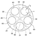
図1は、本発明の第1実施形態に係る半導体製造装置の概略断面図である。この図に示されるように、半導体製造装置は、処理チャンバ10と、サセプタ20と、シャフト30と、ハロゲンランプ40と、回転機構50とを備えている。
FIG. 1 is a schematic cross-sectional view of a semiconductor manufacturing apparatus according to the first embodiment of the present invention. As shown in this figure, the semiconductor manufacturing apparatus includes a
処理チャンバ10は、大気圧から減圧されて成膜ガスが注入される処理室11を備え、この処理室11内で半導体ウエハ60を加熱処理するためのものである。具体的に、処理チャンバ10は、石英ドーム12、13と冷却チャンバ14、15とを備えて構成されている。
The
石英ドーム12、13は、石英窓12a、13aとフランジ部12b、13bとで構成されている。石英窓12a、13aは処理室11の境界の一部を形成するように配置され、処理室11より外側に向けて凸状となっている容器である。また、フランジ部12b、13bは石英窓12a、13aの開口端部に設けられたものである。そして、冷却チャンバ14、15は、Oリング16、17を介して石英ドーム12、13のフランジ部12b、13bを拘束するものであり、内部に冷却水が流れる構造を有している。
The quartz domes 12 and 13 are composed of
石英ドーム12、13のフランジ部12b、13bにOリング16、17を介して冷却チャンバ14、15が固定されたものが2つ用意され、各石英ドーム12、13の各石英窓12a、13aの凹部がそれぞれ向かい合わされて、各冷却チャンバ14、15が接合されて処理チャンバ10が構成されている。このように、石英ドーム12、13、Oリング16、17、および冷却チャンバ14、15にて閉じられた空間が処理室11となる。
Two of the quartz domes 12 and 13 are prepared by fixing the cooling
サセプタ20は、一面21および他面22を有し、一面21に複数の半導体ウエハ60が配置される円板状のテーブルである。
The
シャフト30は、サセプタ20を支持して当該サセプタ20を処理チャンバ10内に配置させるものであり、メインシャフト31と複数のアーム32とを備えている。
The
メインシャフト31は、サセプタ20の他面22側に位置すると共に、サセプタ20の他面22に対し垂直方向に延びる棒状の部材である。メインシャフト31のうちサセプタ20側の上端部31a側にサセプタ20が配置され、上端部31aとは反対側の下端部31bが回転機構50に備え付けられている。
The
図1に示されるように、メインシャフト31は、石英窓13aに設けられたメインシャフト貫通部13cに差し込まれた形態になっている。これにより、メインシャフト31の上端部31aは処理室11内に配置され、下端部31bは処理室11の外部に配置されている。
As shown in FIG. 1, the
アーム32は、メインシャフト31の上端部31aから放射状に延びてサセプタ20の他面22に接続され、サセプタ20を支える部材である。本実施形態では、5本のアーム32がメインシャフト31に設けられており、5本のアーム32でサセプタ20を支えている。なお、図1では1本のアーム32のみを描いてある。
The
図2は、メインシャフト31の上端部31aとアーム32との接続部の一部斜視図を示したものである。この図に示されるように、アーム32のうちメインシャフト31の中心軸に平行な面32aと、メインシャフト31の側面31cとの接続部が面取りされている。
FIG. 2 is a partial perspective view of a connection portion between the
これによると、図2の破線にて示されるように、アーム32の面32aとメインシャフト31の側面31cとが略直角に交わる場合よりも、メインシャフト31に対するアーム32の接続部を肉厚にすることができ、当該接続部に生じる応力を低減することができる。すなわち、アーム32を細くしても、アーム32がサセプタ20の荷重に耐えられる。
According to this, as shown by the broken line in FIG. 2, the connecting portion of the
アーム32とメインシャフト31との接続部の形状によって、アーム32の面32aとメインシャフト31の側面31cとが略直角に交わる場合のアーム32よりも、アーム32の太さを20%細くすることができる。つまり、ハロゲンランプ40の光を遮るアーム32の面積を小さくすることができ、ひいては半導体ウエハ60をより均熱化することができる。
The thickness of the
なお、図2では、アーム32とメインシャフト31との接続部を一箇所のみ示してあるが、実際には全ての接続部において面取りされている。
In FIG. 2, only one connecting portion between the
また、図1に示されるハロゲンランプ40は、輻射熱を発する加熱源であり、処理チャンバ10の外部に複数配置されている。具体的には、ハロゲンランプ40は、各石英窓12a、13aに対向する場所に配置され、サセプタ20の一面21および他面22を照らし加熱するようになっている。
Further, the
回転機構50は、メインシャフト31の下端部31bを支持し、メインシャフト31の中心軸を中心にメインシャフト31を回転させるものであり、モータ等を備えた周知のものである。この回転機構50によってメインシャフト31が回転すると、これに連動してアーム32も回転し、ひいてはアーム32に支持されたサセプタ20も回転するようになっている。
The
この回転機構50によってサセプタ20を回転することで、サセプタ20の周方向に対してハロゲンランプ40の配置位置のばらつきやハロゲンランプ40の照度のばらつきがあったとしても、半導体ウエハ60においてサセプタ20の周方向の温度分布を無くすことができる。
By rotating the
以上が、本実施形態に係る半導体製造装置の全体構成である。この半導体製造装置において、ハロゲンランプ40の照度や回転機構50の回転速度、処理室11への成膜ガスの注入、冷却チャンバ14、15の冷却水の制御等は、図示しない制御装置により行われる。
The above is the overall configuration of the semiconductor manufacturing apparatus according to the present embodiment. In this semiconductor manufacturing apparatus, the illuminance of the
次に、上記装置において、サセプタ20の一面21に配置する半導体ウエハ60とシャフト30との関係について説明する。図3は、サセプタ20の一面21を半導体ウエハ60が配置される側から見た平面図である。
Next, the relationship between the
まず、図3の平面図に示されるように、サセプタ20の一面21に垂直な方向で、メインシャフト31の上端部31aおよび各アーム32と半導体ウエハ60とが離間していると共に、各アーム32の間に半導体ウエハ60が配置されている。
First, as shown in the plan view of FIG. 3, the
このような配置関係により、下側のハロゲンランプ40から見た場合に各半導体ウエハ60がメインシャフト31の上端部31aやアーム32の影にならない。すなわち、メインシャフト31の上端部31aやアーム32が半導体ウエハ60に対してハロゲンランプ40の輻射熱を阻害しないため、各半導体ウエハ60がそれぞれ均一に加熱されることになる。
Due to such an arrangement relationship, each
また、サセプタ20の一面21に半導体ウエハ60が配置された状態で、サセプタ20の他面22とアーム32との接続点23が、半導体ウエハ60のうちメインシャフト31の中心軸からもっとも離れた位置よりもメインシャフト30の中心軸側に位置していることが望ましい。
Further, in a state where the
このように接続点23の位置を規定する理由は、サセプタ20の熱の逃げの経路を制限するためである。ハロゲンランプ40によって加熱されたサセプタ20の熱は、サセプタ20から冷却チャンバ14、15側に逃げる。また、サセプタ20の熱は、サセプタ20の他面22とアーム32との接続点23を介してアーム32を経由し、メインシャフト31にも逃げる。このような熱の逃げの二経路が近い場所にあると、二経路から熱が逃げていくため、当該二経路に近い場所の温度が周囲よりも下がってしまう。これを回避するため、熱が逃げる経路の一部をなす上記接続点23の位置を規定することで、サセプタ20の外周側への新たな熱の逃げの経路を作らないようにしている。このようして、サセプタ20の外径方向に温度分布が形成されないようにして半導体ウエハ60の均熱化を図る。
The reason for defining the position of the
さらに、サセプタ20の一面21に半導体ウエハ60が配置された状態で、サセプタ20の一面21の面方向において、半導体ウエハ60の側面とサセプタ20の側面との最短距離をbとし、半導体ウエハ60の側面と接続点23との最短距離をcとしたとき、c>bの条件を満たすように半導体ウエハ60をサセプタ20に配置する。このように規定することにより、サセプタ20の熱の主な逃げの経路をサセプタ20の外周部に限定して、アーム32の接続点23を介してアーム32側に熱を逃がしにくくする。その結果、外周部への熱の逃げに限定した設計ができ設計が簡単になる。
Further, in a state where the
そして、本実施形態では、サセプタ20の他面22側に配置されるハロゲンランプ40の数と、サセプタ20の一面21に配置される半導体ウエハ60の数と、アーム32の数とが同じである。このように、サセプタ20の他面22側に配置されるハロゲンランプ40の数を規定するのは、アーム32の影ができるサセプタ20の他面22側において、半導体ウエハ60とアーム32とハロゲンランプ40との関係を全ての半導体ウエハ60に対して対称にして、各半導体ウエハ60で温度がばらつかないようにするためである。サセプタ20の一面21側においては、ハロゲンランプ40を配置しない場合でもこの効果は有効である。本実施形態では、サセプタ20の一面21側にもハロゲンランプ40を配置している。
In this embodiment, the number of
図4は、半導体ウエハ60とアーム32とハロゲンランプ40との位置関係を示した平面図であり、図3に相当する図である。この図に示されるように、サセプタ20の一面21に半導体ウエハ60が配置された状態であり、さらにサセプタ20が停止した状態において、サセプタ20の一面に垂直な方向で各ハロゲンランプ40と半導体ウエハ60とが重なるようにハロゲンランプ40が配置されている。これは、サセプタ20の一面21側および他面22側の両方向において、処理チャンバ10の外部にハロゲンランプ40がそれぞれ配置されている。
FIG. 4 is a plan view showing the positional relationship among the
これによると、半導体ウエハ60とアーム32とハロゲンランプ40との関係が全ての半導体ウエハ60に対して対称になり、全ての半導体ウエハ60を均一に熱処理することが可能となる。
According to this, the relationship among the
次に、上記装置およびサセプタ20や半導体ウエハ60の位置関係に基づいて、半導体ウエハ60に熱処理を行う工程について説明する。
Next, a process of performing a heat treatment on the
まず、処理チャンバ10が開けられた状態で、サセプタ20の一面21に図3および図4の配置関係となるように半導体ウエハ60を配置する。続いて、処理チャンバ10を閉めて処理室11が処理チャンバ10の外部と隔離されるようにする。
First, in a state where the
この後、処理室11を大気圧から減圧して真空状態とし、処理室11内に成膜ガスを流し込む。また、ハロゲンランプ40で処理チャンバ10内を加熱すると共に、回転機構50を駆動してサセプタ20を回転させる。その状態で成膜ガス(例えばジクロロシラン)を処理チャンバ10内に導入する。これにより、半導体ウエハ60に成膜する。
Thereafter, the
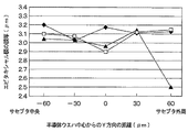
発明者らは、半導体ウエハ60にエピタキシャル膜を成長させて膜厚を調べた。その結果を図5および図6に示す。ここで、図7に示されるように、半導体ウエハ60においてサセプタ20の外径方向を+Y方向とし、+Y方向に垂直な方向において半導体ウエハ60が時計回りの方向に回転させられる方向を+X方向としている。
The inventors have grown an epitaxial film on the
図5および図6では、サセプタ20の一面に垂直な方向において、「▲」はアーム32が半導体ウエハ60と重なり、接続点23の位置がサセプタ20の外周側に配置される第1の場合、「□」はアーム32が半導体ウエハ60と重なり、接続点23の位置が半導体ウエハ60の中心に配置される第2の場合、「◆」はアーム32が半導体ウエハ60と重ならずに、図3の配置関係が満たされた本実施形態の場合を示している。
5 and 6, in the direction perpendicular to one surface of the
そして、第1の場合では、図5に示されるように、サセプタ20の外径方向への熱の逃げが影響するため、+Y方向(サセプタ20の外周側)で+Y方向よりも膜厚が小さくなっている。同様に、図6に示されるように、X方向においては半導体ウエハ60の中心部で膜厚が小さくなっている。
In the first case, as shown in FIG. 5, since the heat escape in the outer diameter direction of the
第2の場合では、図5に示されるように、Y方向での膜厚の薄膜化は見られないが、接続点が半導体ウエハ60の中心部に位置しているため、当該接続点23を介して熱が逃げることにより、図6に示されるように、半導体ウエハ60の中央部では若干の膜厚の薄膜化が見られる。アーム32で半導体ウエハ60の中心部が覆われている影響も見られる。
In the second case, as shown in FIG. 5, although the film thickness is not reduced in the Y direction, the connection point is located at the center of the
しかしながら、本実施形態の場合では、アーム32が半導体ウエハ60の表面を覆っていない、すなわち半導体ウエハ60の影にならないので、図5および図6に示されるように、均一な膜厚分布となっている。また、熱の逃げの経路が分散されているため、半導体ウエハ60が均一に加熱され、膜厚が均一になっているとも言える。このような結果からも、アーム32から半導体ウエハ60が離間していることや接続点23の位置を規定することで半導体ウエハ60の均熱化が図られ、均一な膜を形成できることがわかる。
However, in the case of the present embodiment, the
この場合、回転機構50によってサセプタ20を回転させることにより、半導体ウエハ60においてサセプタ20の周方向の温度分布を無くすことができる。これによっても、半導体ウエハ60の均熱化を図ることができる。
In this case, by rotating the
均一な膜を形成できる他、半導体ウエハ60の成膜における膜厚制御や不純物濃度の制御性を向上させることも可能となる。さらに、半導体ウエハ60を均熱化することができることから、半導体ウエハ60の温度が不均一になることで半導体ウエハ60に応力が生じるスリップ発生を防止することも可能となる。
In addition to forming a uniform film, it is possible to improve film thickness control and impurity concentration controllability in the formation of the
以上説明したように、本実施形態では、サセプタ20の一面21に垂直な方向で、メインシャフト31の上端部31aおよび各アーム32と半導体ウエハ60とが離間していると共に、各アーム32の間に半導体ウエハ60が配置されていることが特徴となっている。
As described above, in the present embodiment, the
これにより、各半導体ウエハ60がアーム32の影にならないようにすることができ、アーム32がハロゲンランプ40の輻射熱を阻害しないようにすることが可能となる。したがって、各半導体ウエハ60をそれぞれ均一に加熱することができる。
Thereby, each
また、半導体ウエハ60とアーム32との位置関係、サセプタ20とアーム32との接続点23の位置を規定することによっても、半導体ウエハ60の均熱化を図ることができる。
Further, by regulating the positional relationship between the
(第2実施形態)
本実施形態では、第1実施形態と異なる部分についてのみ説明する。上記第1実施形態では、サセプタ20の一面21に垂直な方向で、アーム32と半導体ウエハ60とが離間しており、各アーム32の間に半導体ウエハ60が配置されていたが、本実施形態では、半導体ウエハ60とアーム32との数が同じであり、メインシャフト31の中心軸を中心に、半導体ウエハ60とアーム32とが回転対称となるように配置されていることを特徴としている。
(Second Embodiment)
In the present embodiment, only different parts from the first embodiment will be described. In the first embodiment, the
すなわち、半導体ウエハ60とアーム32とが回転対称となるように配置されていれば、サセプタ20の一面21に垂直な方向で、アーム32と半導体ウエハ60とが離間していなくても良いし、各アーム32の間に半導体ウエハ60が配置されていなくても良い。また、c>bの条件も満たしていなくても良い。なお、装置については図1に示されるものが採用される。
That is, if the
図8は、本実施形態においてサセプタ20に半導体ウエハ60を配置したときの平面図であり、図3に相当する図である。図8(a)はサセプタ20の一面21から見た平面図である。図8(b)は、サセプタ20の他面22を下のハロゲンランプ40側から見た平面図である。図8(a)に示されるように、メインシャフト31の中心軸を中心に、半導体ウエハ60とアーム32とが回転対称となるように配置されている。また、サセプタ20の一面21に垂直な方向で、アーム32と半導体ウエハ60とがオーバーラップしている。
FIG. 8 is a plan view when the
サセプタ20の他面22側に配置されるハロゲンランプ40の数についても、サセプタ20の一面21に配置される半導体ウエハ60の数およびアーム32の数と同じになっている。図8(b)に示されるように、半導体ウエハ60とアーム32とハロゲンランプ40とが回転対称になるように、それぞれが配置されている。
The number of
このような配置関係によって半導体ウエハ60にエピタキシャル膜を成長させると、図5および図6において「□」によって表される膜厚となる。この場合であっても、回転機構50によってサセプタ20を回転させることで、各半導体ウエハ60を同じように加熱することができ、さらには各半導体ウエハ60を均熱化することができるので、「▲」の場合よりも膜厚を均等にすることができる。
When an epitaxial film is grown on the
また、サセプタ20の他面22にアーム32による影ができていても、サセプタ20が回転することにより、ハロゲンランプ40の光が届きにくい部分にハロゲンランプ40の熱を届かせることができる。これにより、アーム32によって影となる部分の熱の不足分が補われ、半導体ウエハ60内での温度分布を回避して半導体ウエハ60内での均熱化が図られる。これにより、図5に示されるように、特に半導体ウエハ60のうち+Y方向の膜厚の減少が回避されている。
Moreover, even if the
以上のように、半導体ウエハ60とアーム32との関係を全ての半導体ウエハ60に対して回転対称に配置することで、各半導体ウエハ60を対称に熱処理することが可能となる。また、ハロゲンランプ40についてもアーム32および半導体ウエハ60と同じ数だけ設け、それぞれについて回転対称に配置することで、半導体ウエハ60とアーム32とハロゲンランプ40との対称性をさらに向上させることが可能となる。
As described above, by arranging the relationship between the
(第3実施形態)
本実施形態では、第1実施形態と異なる部分についてのみ説明する。本実施形態では、第1実施形態における半導体ウエハ60とアーム32との配置関係のうち、サセプタ20の他面22とアーム32との接続点23が、半導体ウエハ60のうちメインシャフト31の中心軸からもっとも離れた位置よりもメインシャフト30の中心軸側に位置していることのみを規定することが特徴となっている。
(Third embodiment)
In the present embodiment, only different parts from the first embodiment will be described. In the present embodiment, of the arrangement relationship between the
すなわち、サセプタ20の一面21に垂直な方向で、アーム32と半導体ウエハ60とが離間していなくても良いし、各アーム32の間に半導体ウエハ60が配置されていなくても良い。もちろん、c>bの条件も満たしていなくても良い。なお、装置については図1に示されるものが採用される。
That is, the
本実施形態におけるアーム32と半導体ウエハ60との配置関係は、例えば図8に示される場合と同じである。このような配置関係により、サセプタ20から処理チャンバ10に逃げる熱の経路に新たな熱の逃げの経路を形成しないようにして、半導体ウエハ60に熱分布が形成されないようにしている。
The positional relationship between the
また、本実施形態では、半導体ウエハ60とアーム32との数が同じである。そして、メインシャフト31の中心軸を中心に、半導体ウエハ60とアーム32とが回転対称となるように配置されている。
In the present embodiment, the number of the
さらに、図8(b)に示されるように、サセプタ20の他面22側にハロゲンランプ40を配置するに際し、当該ハロゲンランプ40の数をサセプタ20の一面21に配置される半導体ウエハ60の数およびアーム32の数と同じにして、メインシャフト31の中心軸を中心に、半導体ウエハ60とアーム32とハロゲンランプ40とを回転対称に配置する。
Further, as shown in FIG. 8B, when the
これにより、半導体ウエハ60、アーム32、およびハロゲンランプ40の関係が全ての半導体ウエハ60に対して回転対称になり、各半導体ウエハ60を均熱化して熱処理することが可能となる。
As a result, the relationship between the
以上のように、サセプタ20とアーム32との接続点23の位置のみを規定して、サセプタ20の外周部に新たな熱の逃げを作らないようにすることだけでも、半導体ウエハ60の均熱化を図ることができる。
As described above, the temperature equalization of the
(他の実施形態)
図1に示される装置の構成は一例を示したものであり、当該構成に限定されるものではない。例えば、処理チャンバ10が他の形状や他の部品によって構成されていても構わない。
(Other embodiments)
The configuration of the apparatus shown in FIG. 1 is an example, and is not limited to the configuration. For example, the
上記各実施形態では、半導体ウエハ60を5枚、アーム32を5本、ハロゲンランプ40を5個としているが、これらは一例を示したものであり、これらの数に限らず、他の数であっても構わない。この場合、例えば第1実施形態については、アーム32の数と半導体ウエハ60の数とが同じである必要はなく、例えば5本のアーム32に対して3枚の半導体ウエハ60をサセプタ20に配置する場合であっても、第1実施形態で規定された配置の条件を満たすようにすることができる。
In each of the above-described embodiments, five
第1実施形態では、ハロゲンランプ40の数と、半導体ウエハ60の数と、アーム32の数とが同じであると説明したが、ハロゲンランプ40の数に関わらず、サセプタ20の一面21に配置される半導体ウエハ60の数と、アーム32の数とが同じとしても良い。このようにしても、各半導体ウエハ60がアーム32の影にならないようにすることができ、アーム32がハロゲンランプ40の輻射熱を阻害しないようにすることができるので、各半導体ウエハ60をそれぞれ均一に加熱することができ、半導体ウエハ60内での膜厚の均一化を図ることができる。
In the first embodiment, it has been described that the number of
10 処理チャンバ
20 サセプタ
21 半導体ウエハの一面
22 半導体ウエハの他面
23 接続点
30 シャフト
31 メインシャフト
31a メインシャフトの上端部
31b メインシャフトの下端部
31c メインシャフトの側面
32 アーム
32a アームの面
40 ハロゲンランプ
50 回転機構
60 半導体ウエハ
DESCRIPTION OF
Claims (13)
前記サセプタ(20)の他面(22)側に位置すると共に、前記サセプタ(20)の他面(22)に対し垂直方向に延びる棒状のメインシャフト(31)と、該メインシャフト(31)のうち前記サセプタ(20)側の上端部(31a)から放射状に延びて前記サセプタ(20)の他面(22)に接続される複数のアーム(32)とを有するシャフト(30)と、
前記サセプタ(20)の他面(22)側であって、前記処理チャンバ(10)の外部に配置され、加熱源となるハロゲンランプ(40)とを有する半導体製造装置であって、
前記サセプタ(20)の一面(21)に垂直な方向で、前記メインシャフト(31)の上端部(31a)および前記各アーム(32)と前記半導体ウエハ(60)とが離間していると共に、前記各アーム(32)の間に前記半導体ウエハ(60)が配置されていることを特徴とする半導体製造装置。 A susceptor (20) disposed in the processing chamber (10), having one surface (21) and the other surface (22), wherein a plurality of semiconductor wafers (60) are disposed on the one surface (21);
A rod-shaped main shaft (31) located on the other surface (22) side of the susceptor (20) and extending in a direction perpendicular to the other surface (22) of the susceptor (20), and a main shaft (31) A shaft (30) having a plurality of arms (32) extending radially from an upper end (31a) on the susceptor (20) side and connected to the other surface (22) of the susceptor (20);
A semiconductor manufacturing apparatus having a halogen lamp (40) on the other surface (22) side of the susceptor (20) and disposed outside the processing chamber (10) and serving as a heating source;
In the direction perpendicular to the one surface (21) of the susceptor (20), the upper end portion (31a) of the main shaft (31) and the arms (32) are separated from the semiconductor wafer (60), and A semiconductor manufacturing apparatus, wherein the semiconductor wafer (60) is disposed between the arms (32).
前記サセプタ(20)の他面(22)側に位置すると共に、前記サセプタ(20)の他面(22)に対し垂直方向に延びる棒状のメインシャフト(31)と、該メインシャフト(31)の上端部(31a)から放射状に延びて前記サセプタ(20)の他面(22)に接続される複数のアーム(32)とを有するシャフト(30)と、
前記サセプタ(20)の他面(22)側であって、前記処理チャンバ(10)の外部に配置され、加熱源となるハロゲンランプ(40)と、
前記メインシャフト(31)の下端部(31b)に前記メインシャフト(31)の中心軸を中心に前記サセプタ(20)を回転させる回転機構(50)とを有する半導体製造装置であって、
前記半導体ウエハ(60)と前記アーム(32)との数が同じであり、前記メインシャフト(31)の中心軸を中心に、前記半導体ウエハ(60)と前記アーム(32)とが回転対称となるように配置されていることを特徴とする半導体製造装置。 A susceptor (20) disposed in the processing chamber (10), having one surface (21) and the other surface (22), wherein a plurality of semiconductor wafers (60) are disposed on the one surface (21);
A rod-shaped main shaft (31) located on the other surface (22) side of the susceptor (20) and extending in a direction perpendicular to the other surface (22) of the susceptor (20), and a main shaft (31) A shaft (30) having a plurality of arms (32) extending radially from the upper end (31a) and connected to the other surface (22) of the susceptor (20);
A halogen lamp (40) on the other surface (22) side of the susceptor (20), disposed outside the processing chamber (10) and serving as a heating source;
A semiconductor manufacturing apparatus having a rotation mechanism (50) for rotating the susceptor (20) about a central axis of the main shaft (31) at a lower end (31b) of the main shaft (31),
The number of the semiconductor wafer (60) and the arm (32) is the same, and the semiconductor wafer (60) and the arm (32) are rotationally symmetric about the central axis of the main shaft (31). The semiconductor manufacturing apparatus is arranged so as to be.
前記サセプタ(20)の他面(22)側に位置すると共に、前記サセプタ(20)の他面(22)に対し垂直方向に延びる棒状のメインシャフト(31)と、該メインシャフト(31)の上端部(31a)から放射状に延びて前記サセプタ(20)の他面(22)に接続される複数のアーム(32)とを有するシャフト(30)と、
前記サセプタ(20)の他面(22)側であって、前記処理チャンバ(10)の外部に配置され、加熱源となるハロゲンランプ(40)とを有する半導体製造装置であって、
前記サセプタ(20)の他面(22)と前記アーム(32)との接続点(23)が、前記半導体ウエハ(60)のうち前記メインシャフト(31)の中心軸からもっとも離れた位置よりも前記メインシャフト(31)の中心軸側に位置していることを特徴とする半導体製造装置。 A susceptor (20) disposed in the processing chamber (10), having one surface (21) and the other surface (22), wherein a plurality of semiconductor wafers (60) are disposed on the one surface (21);
A rod-shaped main shaft (31) located on the other surface (22) side of the susceptor (20) and extending in a direction perpendicular to the other surface (22) of the susceptor (20), and a main shaft (31) A shaft (30) having a plurality of arms (32) extending radially from the upper end (31a) and connected to the other surface (22) of the susceptor (20);
A semiconductor manufacturing apparatus having a halogen lamp (40) on the other surface (22) side of the susceptor (20) and disposed outside the processing chamber (10) and serving as a heating source;
The connection point (23) between the other surface (22) of the susceptor (20) and the arm (32) is located farthest from the central axis of the main shaft (31) in the semiconductor wafer (60). The semiconductor manufacturing apparatus is located on the central axis side of the main shaft (31).
前記サセプタ(20)に複数の半導体ウエハ(60)を配置し、前記ハロゲンランプ(40)により前記処理チャンバ(10)内を加熱して、前記処理チャンバ(10)内に反応ガスを流し込んで前記半導体ウエハ(60)に成膜することを特徴とする半導体装置の製造方法。 A method of manufacturing a semiconductor device using the semiconductor manufacturing apparatus according to any one of claims 1 to 12,
A plurality of semiconductor wafers (60) are disposed on the susceptor (20), the inside of the processing chamber (10) is heated by the halogen lamp (40), and a reaction gas is flowed into the processing chamber (10) to A method of manufacturing a semiconductor device, comprising forming a film on a semiconductor wafer (60).
Priority Applications (1)
| Application Number | Priority Date | Filing Date | Title |
|---|---|---|---|
| JP2008024843A JP5145984B2 (en) | 2008-02-05 | 2008-02-05 | Semiconductor manufacturing apparatus and semiconductor device manufacturing method using the same |
Applications Claiming Priority (1)
| Application Number | Priority Date | Filing Date | Title |
|---|---|---|---|
| JP2008024843A JP5145984B2 (en) | 2008-02-05 | 2008-02-05 | Semiconductor manufacturing apparatus and semiconductor device manufacturing method using the same |
Publications (2)
| Publication Number | Publication Date |
|---|---|
| JP2009188082A JP2009188082A (en) | 2009-08-20 |
| JP5145984B2 true JP5145984B2 (en) | 2013-02-20 |
Family
ID=41071054
Family Applications (1)
| Application Number | Title | Priority Date | Filing Date |
|---|---|---|---|
| JP2008024843A Active JP5145984B2 (en) | 2008-02-05 | 2008-02-05 | Semiconductor manufacturing apparatus and semiconductor device manufacturing method using the same |
Country Status (1)
| Country | Link |
|---|---|
| JP (1) | JP5145984B2 (en) |
Families Citing this family (6)
| Publication number | Priority date | Publication date | Assignee | Title |
|---|---|---|---|---|
| JP5446760B2 (en) * | 2009-11-16 | 2014-03-19 | 株式会社Sumco | Epitaxial growth method |
| KR101108576B1 (en) | 2010-04-08 | 2012-01-30 | 국제엘렉트릭코리아 주식회사 | Susceptor and vertical substrates treatment equipment with the same |
| TW201218301A (en) * | 2010-10-28 | 2012-05-01 | Applied Materials Inc | Apparatus having improved substrate temperature uniformity using direct heating methods |
| KR101819095B1 (en) | 2013-03-15 | 2018-01-16 | 어플라이드 머티어리얼스, 인코포레이티드 | Susceptor support shaft with uniformity tuning lenses for epi process |
| JP6539568B2 (en) | 2015-11-04 | 2019-07-03 | 株式会社Screenホールディングス | Heat treatment method and heat treatment apparatus |
| KR101813674B1 (en) * | 2016-03-03 | 2017-12-29 | (주) 씨앤아이테크놀로지 | Sputtering system |
Family Cites Families (2)
| Publication number | Priority date | Publication date | Assignee | Title |
|---|---|---|---|---|
| JP3076791B2 (en) * | 1998-10-19 | 2000-08-14 | アプライド マテリアルズ インコーポレイテッド | Semiconductor manufacturing equipment |
| US7169234B2 (en) * | 2004-01-30 | 2007-01-30 | Asm America, Inc. | Apparatus and methods for preventing rotational slippage between a vertical shaft and a support structure for a semiconductor wafer holder |
-
2008
- 2008-02-05 JP JP2008024843A patent/JP5145984B2/en active Active
Also Published As
| Publication number | Publication date |
|---|---|
| JP2009188082A (en) | 2009-08-20 |
Similar Documents
| Publication | Publication Date | Title |
|---|---|---|
| JP5145984B2 (en) | Semiconductor manufacturing apparatus and semiconductor device manufacturing method using the same | |
| US5884009A (en) | Substrate treatment system | |
| JP5038365B2 (en) | Susceptor and deposition system | |
| JPH0897167A (en) | Processing system and heat-treatment system | |
| US6031205A (en) | Thermal treatment apparatus with thermal protection members intercepting thermal radiation at or above a predetermined angle | |
| JPH09260364A (en) | Thermal treatment method and thermal treatment equipment | |
| JP3853587B2 (en) | Substrate processing apparatus and semiconductor device manufacturing method | |
| US7591908B2 (en) | Vapor deposition apparatus and vapor deposition method | |
| JP2002151412A (en) | Semiconductor manufacturing apparatus | |
| US8968475B2 (en) | Substrate processing apparatus | |
| TWI697364B (en) | One-piece injector assembly, lower liner, and apparatus for substrate processing including the same | |
| KR20230074248A (en) | vapor growth device | |
| JP2001319886A (en) | System and method for heat treatment | |
| KR101633557B1 (en) | Semiconductor manufacturing apparatus and semiconductor manufacturing method | |
| JP2002155366A (en) | Method and device of leaf type heat treatment | |
| JP2000349038A (en) | Substrate treating device | |
| KR20110086286A (en) | Chemical vapor deposition device | |
| US20160244878A1 (en) | Substrate processing apparatus and heating unit | |
| JPH08124869A (en) | Vertical heat treating apparatus | |
| JP5999511B2 (en) | Vapor phase epitaxial growth apparatus and epitaxial wafer manufacturing method using the same | |
| KR20140058270A (en) | Batch type semiconductor manufacturing device | |
| JPH08148480A (en) | Semiconductor manufacturing device and method | |
| JP2006294779A (en) | Heat processing furnace | |
| JP2976240B2 (en) | Heat treatment furnace | |
| JP2000150405A (en) | Heat treatment device for substrate and temperature compensating ring |
Legal Events
| Date | Code | Title | Description |
|---|---|---|---|
| A621 | Written request for application examination |
Free format text: JAPANESE INTERMEDIATE CODE: A621 Effective date: 20101201 |
|
| A977 | Report on retrieval |
Free format text: JAPANESE INTERMEDIATE CODE: A971007 Effective date: 20111031 |
|
| TRDD | Decision of grant or rejection written | ||
| A01 | Written decision to grant a patent or to grant a registration (utility model) |
Free format text: JAPANESE INTERMEDIATE CODE: A01 Effective date: 20121030 |
|
| A61 | First payment of annual fees (during grant procedure) |
Free format text: JAPANESE INTERMEDIATE CODE: A61 Effective date: 20121112 |
|
| R150 | Certificate of patent or registration of utility model |
Ref document number: 5145984 Country of ref document: JP Free format text: JAPANESE INTERMEDIATE CODE: R150 Free format text: JAPANESE INTERMEDIATE CODE: R150 |
|
| FPAY | Renewal fee payment (event date is renewal date of database) |
Free format text: PAYMENT UNTIL: 20151207 Year of fee payment: 3 |
|
| R250 | Receipt of annual fees |
Free format text: JAPANESE INTERMEDIATE CODE: R250 |
|
| S111 | Request for change of ownership or part of ownership |
Free format text: JAPANESE INTERMEDIATE CODE: R313117 |
|
| R350 | Written notification of registration of transfer |
Free format text: JAPANESE INTERMEDIATE CODE: R350 |
|
| R250 | Receipt of annual fees |
Free format text: JAPANESE INTERMEDIATE CODE: R250 |
|
| R250 | Receipt of annual fees |
Free format text: JAPANESE INTERMEDIATE CODE: R250 |
|
| R250 | Receipt of annual fees |
Free format text: JAPANESE INTERMEDIATE CODE: R250 |
|
| R250 | Receipt of annual fees |
Free format text: JAPANESE INTERMEDIATE CODE: R250 |
|
| R250 | Receipt of annual fees |
Free format text: JAPANESE INTERMEDIATE CODE: R250 |
|
| R250 | Receipt of annual fees |
Free format text: JAPANESE INTERMEDIATE CODE: R250 |
|
| R250 | Receipt of annual fees |
Free format text: JAPANESE INTERMEDIATE CODE: R250 |
|
| R250 | Receipt of annual fees |
Free format text: JAPANESE INTERMEDIATE CODE: R250 |