JP5141237B2 - Semiconductor memory device, manufacturing method thereof, writing method and reading method - Google Patents
Semiconductor memory device, manufacturing method thereof, writing method and reading method Download PDFInfo
- Publication number
- JP5141237B2 JP5141237B2 JP2007330271A JP2007330271A JP5141237B2 JP 5141237 B2 JP5141237 B2 JP 5141237B2 JP 2007330271 A JP2007330271 A JP 2007330271A JP 2007330271 A JP2007330271 A JP 2007330271A JP 5141237 B2 JP5141237 B2 JP 5141237B2
- Authority
- JP
- Japan
- Prior art keywords
- tunnel junction
- magnetic tunnel
- transistor
- bit line
- source
- Prior art date
- Legal status (The legal status is an assumption and is not a legal conclusion. Google has not performed a legal analysis and makes no representation as to the accuracy of the status listed.)
- Expired - Fee Related
Links
Images

Classifications
-
- G—PHYSICS
- G11—INFORMATION STORAGE
- G11C—STATIC STORES
- G11C11/00—Digital stores characterised by the use of particular electric or magnetic storage elements; Storage elements therefor
- G11C11/02—Digital stores characterised by the use of particular electric or magnetic storage elements; Storage elements therefor using magnetic elements
- G11C11/16—Digital stores characterised by the use of particular electric or magnetic storage elements; Storage elements therefor using magnetic elements using elements in which the storage effect is based on magnetic spin effect
- G11C11/165—Auxiliary circuits
- G11C11/1659—Cell access
-
- G—PHYSICS
- G11—INFORMATION STORAGE
- G11C—STATIC STORES
- G11C11/00—Digital stores characterised by the use of particular electric or magnetic storage elements; Storage elements therefor
- G11C11/02—Digital stores characterised by the use of particular electric or magnetic storage elements; Storage elements therefor using magnetic elements
- G11C11/16—Digital stores characterised by the use of particular electric or magnetic storage elements; Storage elements therefor using magnetic elements using elements in which the storage effect is based on magnetic spin effect
- G11C11/165—Auxiliary circuits
- G11C11/1673—Reading or sensing circuits or methods
-
- G—PHYSICS
- G11—INFORMATION STORAGE
- G11C—STATIC STORES
- G11C11/00—Digital stores characterised by the use of particular electric or magnetic storage elements; Storage elements therefor
- G11C11/02—Digital stores characterised by the use of particular electric or magnetic storage elements; Storage elements therefor using magnetic elements
- G11C11/16—Digital stores characterised by the use of particular electric or magnetic storage elements; Storage elements therefor using magnetic elements using elements in which the storage effect is based on magnetic spin effect
- G11C11/165—Auxiliary circuits
- G11C11/1675—Writing or programming circuits or methods
Landscapes
- Engineering & Computer Science (AREA)
- Computer Hardware Design (AREA)
- Mram Or Spin Memory Techniques (AREA)
- Hall/Mr Elements (AREA)
Description
本発明は、広くは半導体記憶装置に関し、特に、1つのトランジスタと2つの磁気トンネル接合(MTJ)素子を有する1T−2MTJメモリセルにおいて、スピン電流の注入により相補的にデータが書き込まれるスピン注入MRAM(Spin Torque Transfer Random Access Memory)の構成と、その動作方法に関する。 The present invention relates generally to semiconductor memory devices, and more particularly to a spin injection MRAM in which data is complementarily written by injection of spin current in a 1T-2MTJ memory cell having one transistor and two magnetic tunnel junction (MTJ) elements. The present invention relates to a configuration of (Spin Torque Transfer Random Access Memory) and an operation method thereof.
磁化の方向により抵抗値が変化する磁気抵抗素子が記憶装置に適用され、高速動作の不揮発性メモリとして期待されている。そのような磁気メモリで、より大きな磁気抵抗を得るために、トンネル接合を利用した磁気トンネル接合(MTJ:Magnetic Tunneling Junction)素子が実用化され始めている。 A magnetoresistive element whose resistance value changes depending on the direction of magnetization is applied to a memory device, and is expected as a non-volatile memory operating at high speed. In such a magnetic memory, in order to obtain a larger magnetoresistance, a magnetic tunnel junction (MTJ) element using a tunnel junction has been put into practical use.
MTJは、2つの強磁性層(磁極の向きが回転可能なフリー層と、磁極の向きが固定されるピンド層)の間に、薄い絶縁層(トンネルバリア層)を挿入したものであり、強磁性層間に電圧を印加すると、スピンを保存したままトンネル電流が流れる。MTJでは、絶縁層を介した強磁性層間の波動関数の重なりがほとんどないため、交換結合が弱く、小さな磁場で大きなトンネル磁気抵抗を得ることができる。 An MTJ is a thin insulating layer (tunnel barrier layer) inserted between two ferromagnetic layers (a free layer whose magnetic pole direction is rotatable and a pinned layer whose magnetic pole direction is fixed). When a voltage is applied between the magnetic layers, a tunnel current flows while preserving spin. In MTJ, there is almost no overlap of wave functions between ferromagnetic layers through an insulating layer, so exchange coupling is weak and a large tunnel magnetoresistance can be obtained with a small magnetic field.
MTJを用いた磁気メモリの書き込み方式としては、配線で供給される電流が引き起こす外部磁界によって、MTJの磁化の向きを平行、反平行に変化させる従来の配線電流磁場書き込み方式に代わって、スピン電流を直接MTJに注入して磁化を反転させるスピン注入型の磁気メモリ(MRAM)が注目されている(たとえば、非特許文献1参照)。 As a magnetic memory writing method using MTJ, a spin current is used instead of the conventional wiring current magnetic field writing method in which the direction of magnetization of MTJ is changed in parallel or antiparallel by an external magnetic field caused by a current supplied by wiring. Attention has been focused on a spin-injection type magnetic memory (MRAM) that inverts magnetization by directly injecting into the MTJ (for example, see Non-Patent Document 1).
図1に、一般的なスピン注入MRAMを示す。1つのメモリセルは、1つのMTJ110と、1つのトランジスタ120で構成される(1T−1MTJ)。MTJ110は、強磁性層であるピンド層111とフリー層113の間に、トンネルバリア層112が挿入されている。トランジスタ120のゲート電極はワード線123に接続され、ソースはソース線122に、ドレインはMTJ110に接続される。MTJ110の他端側は、ビット線121に接続される。
FIG. 1 shows a general spin injection MRAM. One memory cell includes one MTJ 110 and one transistor 120 (1T-1MTJ). In the MTJ 110, a
書き込み時には、ワード線123と、ビット線121、ソース線122を選択することにより、書き込みセルを選択し、書込パルス/読出バイアス生成部131から、選択されたビット線121又はソース線122に電圧を印加して、電流の方向を制御する。
At the time of writing, a
図1(b)に示すように、スピン注入MRAMでは、MTJ110に流す電流の向きを変えて書き込みを行う。たとえば、“0”の書き込みは、白矢印で示すように、ビット線121側から書き込み用のスピン電流を流す。電子はピンド層111に流れ込み、ピンド層111の磁化と同じ向きにスピン編極した電子が、フリー層113へと流れて、フリー層113の磁化の向きをピンド層111のそれと平行にする。これによりMTJ110は、電気抵抗の小さい状態RLになる。逆に、“1”の書き込みはソース線122側から書き込み電流を流す。電子は、フリー層113側からピンド層111へと流れ、ピンド層111の磁化と逆の向きにスピン編極した電子は、反射されてフリー層113へと戻り、フリー層113の磁化の方向をピンド層111と反対の方向(反平行)にする。これによりMTJ110は、電気抵抗の大きい状態RHになる。
As shown in FIG. 1B, in the spin injection MRAM, writing is performed by changing the direction of the current flowing through the
読み出しの一般的な方法は、V=I*Rに基づき、読み出し電圧Vを一定にして電流源から読み出し電流を流し、抵抗変化ΔRによる電流変化ΔIを読む。この方式を、電流読み出し方式という。読み出し電流は、書き込み電流よりも小さく、読み出し電流によってデータが書き換えされないようにしている。 A general method of reading is based on V = I * R, and reads a current change ΔI due to a resistance change ΔR by causing a read current to flow from a current source with a constant read voltage V. This method is called a current readout method. The read current is smaller than the write current, and data is not rewritten by the read current.
一方、スピン注入型ではなく、従来の配線電流磁場書き込み方式のMRAMにおいて、相補的にデータを書き込んで、電圧読み出し方式でデータを読み出す方法が提案されている(たとえば、非特許文献2及び特許文献1参照)。
On the other hand, in a conventional MRAM using a wiring current magnetic field writing method instead of a spin injection type, a method of writing data complementarily and reading data by a voltage reading method has been proposed (for example, Non-Patent
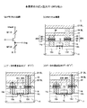
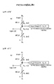
図2に公知の配線電流磁場書き込み方式の1T−2MTJメモリセルの構成を示す。図2(a)に示すように、トランジスタTrの一方の側(ソース側)に直列接続の2つのMTJ(MTJ1及びMTJ2)が配置されている。書き込みは、トランジスタTrをオフにし、ディジット線DLに書き込み電流を流す。書き込み電流は、書き込みワード線WWL1、WWL2にも印加され、図2(b)の点線の矢印で示すように、電流ループが形成される。この電流によって引き起こされる磁場により、2つのMTJ(MTJ1とMTJ2)にデータが相補的に書き込まれる。すなわち、一方のMTJが高抵抗状態のときは、他方のMTJは低抵抗状態となる。電流ループの方向によって“1”書き込みと“0”書き込みがなされる。 FIG. 2 shows a configuration of a known wiring current magnetic field writing system 1T-2MTJ memory cell. As shown in FIG. 2A, two MTJs (MTJ1 and MTJ2) connected in series are arranged on one side (source side) of the transistor Tr. For writing, the transistor Tr is turned off, and a writing current is supplied to the digit line DL. The write current is also applied to the write word lines WWL1 and WWL2, and a current loop is formed as indicated by the dotted arrows in FIG. Data is written to the two MTJs (MTJ1 and MTJ2) in a complementary manner by the magnetic field caused by this current. That is, when one MTJ is in a high resistance state, the other MTJ is in a low resistance state. “1” write and “0” write are performed depending on the direction of the current loop.
読み出し時には、図2(c)に示すように、トランジスタがオンにされ、読み出し電圧Vreadが直列接続されたMTJ1,MTJ2に印加され、MTJ1とMTJ2の間の接続ノードから、読み出し信号Vsigが取り出される。MTJ1が低抵抗、MTJ2が高抵抗(この状態を“1”とする)のときは、読み出し信号VsigはVread/2よりも大きい。MTJ1が高抵抗、MTJ2が低抵抗(この状態を“0”とする)のときは、読み出し信号VsigはVread/2よりも小さい。 At the time of reading, as shown in FIG. 2C, the transistor is turned on, the read voltage Vread is applied to MTJ1 and MTJ2 connected in series, and the read signal Vsig is taken out from the connection node between MTJ1 and MTJ2. . When MTJ1 is low resistance and MTJ2 is high resistance (this state is “1”), the read signal Vsig is larger than Vread / 2. When MTJ1 is high resistance and MTJ2 is low resistance (this state is “0”), the read signal Vsig is smaller than Vread / 2.
相補的にデータを書いて読むことで、メモリセルサイズを小さくすることができ、かつ読み出し動作が安定する。
図1に示すスピン注入MRAMは、素子サイズが小さく、磁性材料を加工するので、1つ1つのMTJ素子120の特性を精度良く揃えることは一般に難しい。また、読み出し電流は、データが書き変わらないように、書き込み電流より小さい値にする必要があり、高集積、大容量のスピン注入MRAMにおいて、読み出しの安定化が課題となっている。
Since the spin injection MRAM shown in FIG. 1 has a small element size and processes a magnetic material, it is generally difficult to align the characteristics of each
さらに、スピン注入MRAMは、電流読み出し方式となっているため、周辺回路として、読み出し電流源(I)回路、読み出し電流の変化(ΔI)を電圧に変換する回路等が必要となり、周辺回路構成が増大する。これに対して、DRAMに代表される一般的なメモリは、基本的に電圧読み出し方式であり、周辺回路は小さい。 Further, since the spin injection MRAM has a current read system, a read current source (I) circuit, a circuit that converts a change in read current (ΔI) into a voltage, and the like are required as peripheral circuits. Increase. On the other hand, a general memory represented by a DRAM is basically a voltage read system and has a small peripheral circuit.
そこで、本発明は、スピン注入MRAMにおいて、電圧読み出し方式のメモリ構成を実現することを課題とする。 Therefore, an object of the present invention is to realize a memory configuration of a voltage read system in a spin injection MRAM.
上記課題を実現するために、第1の側面では、トランジスタのソース・ドレインの両側に、書き込み電流印加時に相補的な抵抗状態をとる2つの磁気トンネル接合素子が直列に接続されている半導体記憶装置が提供される。 In order to achieve the above object, in the first aspect, a semiconductor memory device in which two magnetic tunnel junction elements that take complementary resistance states when a write current is applied are connected in series on both sides of a source and a drain of a transistor Is provided.
第2の側面では、半導体記憶装置は、
トランジスタと、
前記トランジスタのソース・ドレイン拡散層の一方に電気的に接続される第1の磁気トンネル接合素子と、
前記ソース・ドレイン拡散層の他方に電気的に接続される第2の磁気トンネル接合素子と、
を有し、前記第1および第2の磁気トンネル接合素子は、外部から供給される書き込み電流が、前記第1の磁気トンネル接合素子と前記第2の磁気トンネル接合素子において逆方向に流れるように、前記トランジスタに接続される。
In a second aspect, the semiconductor memory device is
A transistor,
A first magnetic tunnel junction element electrically connected to one of the source / drain diffusion layers of the transistor;
A second magnetic tunnel junction element electrically connected to the other of the source / drain diffusion layers;
And the first and second magnetic tunnel junction elements are configured such that an externally supplied write current flows in opposite directions in the first magnetic tunnel junction element and the second magnetic tunnel junction element. , Connected to the transistor.
第3の側面では、複数のメモリセルの配列を含む半導体記憶装置が提供される。この半導体記憶装置は、
互いに隣接し、各々が1つのトランジスタと、前記トランジスタのソース・ドレインの両側に直列に接続される2つの磁気トンネル接合素子と、前記ソース・ドレインのいずれかの側に位置する読み出しノードとを有する第1及び第2のメモリセル、を含み、
前記第1および第2のメモリセルの前記2つの磁気トンネル接合素子の1つに共通に接続される第1のビット線と、
前記第1及び第2のメモリセルの前記読み出しノードに共通に接続される第2のビット線と、
を有する。
In a third aspect, a semiconductor memory device including an array of a plurality of memory cells is provided. This semiconductor memory device
Adjacent to each other, each having one transistor, two magnetic tunnel junction elements connected in series on both sides of the source / drain of the transistor, and a read node located on either side of the source / drain First and second memory cells,
A first bit line commonly connected to one of the two magnetic tunnel junction elements of the first and second memory cells;
A second bit line connected in common to the read nodes of the first and second memory cells;
Have
第4の側面では、複数のメモリセルの配列を有する半導体記憶装置において、
互いに隣接し、各々が1つのトランジスタと、前記トランジスタのソース・ドレインの両側に直列に接続される2つの磁気トンネル接合素子と、前記ソース・ドレインのいずれかの側に位置する読み出しノードとを有する第1及び第2のメモリセル、を含み、
前記第1のメモリセルの一方の磁気トンネル接合素子と、前記第2のメモリセルの前記読み出しノードとが接続される第1のビット線と、
前記第2のメモリセルの一方の磁気トンネル接合素子と、前記第1のメモリセルの前記読み出しノードとが接続される第2のビット線と、
を有する。
In a fourth aspect, in a semiconductor memory device having an array of a plurality of memory cells,
Adjacent to each other, each having one transistor, two magnetic tunnel junction elements connected in series on both sides of the source / drain of the transistor, and a read node located on either side of the source / drain First and second memory cells,
A first bit line connected to one magnetic tunnel junction element of the first memory cell and the read node of the second memory cell;
A second bit line to which one magnetic tunnel junction element of the second memory cell and the read node of the first memory cell are connected;
Have
上記の構成及び手法により、スピン注入MRAMで電圧センス方式を可能にし、読み出しの安定化を図ることができる。また、周辺回路を簡略化することができる。 With the above configuration and method, a voltage sensing method can be realized in the spin injection MRAM, and reading can be stabilized. In addition, the peripheral circuit can be simplified.
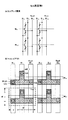
以下、添付図面を参照して、本発明の良好な実施形態を説明する。図3(a)は、本発明の一実施形態のスピン注入型の磁気抵抗メモリ(MRAM)のメモリセル回路図、図3(b)は、半導体記憶装置としてのスピン注入MRAM1の概略断面図、図3(c)および図3(d)は、相補的なデータ書き込みを示す概略図である。
DESCRIPTION OF EXEMPLARY EMBODIMENTS Hereinafter, preferred embodiments of the invention will be described with reference to the accompanying drawings. FIG. 3A is a memory cell circuit diagram of a spin injection type magnetoresistive memory (MRAM) according to an embodiment of the present invention. FIG. 3B is a schematic cross-sectional view of a
図3(a)に示すように、セルトランジスタTrの両側に、2つのMTJ素子、すなわちMTJ1(30A)とMTJ2(30B)が直列接続され、セルトランジスタTrと一方のMTJの接続ノードから、読み出し信号Vsigが取り出される。この例では、セルトランジスタTrのソース側が読み出しノードとなっている。読み出し時には、セルトランジスタTrをオンにして、直列に接続したMTJ1とMTJ2の両側に電圧(読み出し電圧Vreadと接地電圧V0)を印加して、接続ノードの電位を検出する。 As shown in FIG. 3A, two MTJ elements, that is, MTJ1 (30A) and MTJ2 (30B) are connected in series on both sides of the cell transistor Tr, and read from the connection node between the cell transistor Tr and one MTJ. The signal Vsig is taken out. In this example, the source side of the cell transistor Tr is a read node. At the time of reading, the cell transistor Tr is turned on, and voltages (read voltage Vread and ground voltage V 0 ) are applied to both sides of MTJ1 and MTJ2 connected in series to detect the potential of the connection node.
図3(b)に示すように、各MTJ30A、30Bは、磁化の方向が固定された強磁性層であるピンド層31と、磁化の方向が変化可能な強磁性層であるフリー層33と、これらの強磁性層の間に挟まれたトンネルバリア層32を有する。MTJ30A、30Bは、それぞれプラグ14a、14bを介して、セルトランジスタTrの拡散層(ドレイン12d、ソース12s)と電気的に接続される。ドレイン側のMTJ30Aは、プラグ18を介して上層のビット線(BL)21に接続され、ソース側のMTJ30Bは、プラグ64を介してソース線(SL)22に接続される。
As shown in FIG. 3B, each
このように、2つのMTJ30A、30Bを、セルトランジスタTrを挟んで直列接続で配置すると、図3(c)および図3(d)に示すように、データを書き込むときは、矢印で示す電子の流れる方向(又は電流の方向)に応じて、一方のMTJが高抵抗に、他方のMTJが低抵抗になる。したがって、セルトランジスタTrの両側のMTJ素子30に容易に相補的な書き込みを行うことができる。これは、スピン注入方式の優位な特徴である。
As described above, when two
たとえば図3(c)のように、MTJ30B側から書き込み用のスピン電流を流すと、矢印のように、スピン偏極した電子が、MTJ30Aのフリー層33の側から注入され、MTJ30Aのフリー層33の磁化の向きを反平行にして、MTJ30Aを高抵抗状態RHとする。電子流は、セルトランジスタTrを経由し、MTJ30Bに流れ込み、MTJ30Bのフリー層33の磁化の向きを、ピンド層31の磁化の向きと平行にして、MTJ30Bを低抵抗状態RLにする。
For example, as shown in FIG. 3C, when a spin current for writing is applied from the
逆に、図3(d)のように、MTJ30A側から書き込み用のスピン電流を流すと、矢印のように電子はMTJ30Bのフリー層33に流れ込んで、フリー層33の磁化の方向をピンド層31と反平行にして、MTJ30Bを高抵抗状態RHとし、他方のMTJ30Aに流れ込んで、MTJ30BA低抵抗状態RLにする。
On the contrary, as shown in FIG. 3D, when a write spin current is passed from the
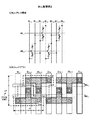
図4および図5に、図3のメモリセル構成を用いたセルアレイの配置例を示す。図4の配置例1では、読み出し専用のビット線ReadBLを設け、ビット線(BL)方向に沿って隣接するメモリセルは、同じソース線SLとビット線BL上に配置される。図4(a)のセルアレイ構成に示すように、あるメモリセルのドレイン側MTJがビット線BL1に接続され、ソース側MTJがソース線SL1に接続され、読み出しノードが読み出しビット線ReadBL1に接続されると、ビット線方向の隣接セルも、同じビット線BL1、ソース線SL1、読み出しビット線ReadBL1に接続されて、縦一列に並ぶ。同様に、次のカラムにおいても、ビット線方向に隣接する複数のメモリセルは、同じビット線BL2、ソース線SL2、読み出しビット線ReadBL2に接続され、縦一列に並ぶ。 4 and 5 show examples of the arrangement of the cell array using the memory cell configuration of FIG. In the arrangement example 1 of FIG. 4, a read-only bit line ReadBL is provided, and adjacent memory cells along the bit line (BL) direction are arranged on the same source line SL and bit line BL. As shown in the cell array configuration of FIG. 4A, the drain side MTJ of a certain memory cell is connected to the bit line BL 1 , the source side MTJ is connected to the source line SL 1 , and the read node is connected to the read bit line ReadBL 1 . When connected, adjacent cells in the bit line direction are also connected to the same bit line BL 1 , source line SL 1 , and read bit line ReadBL 1, and are aligned in a vertical row. Similarly, in the next column, a plurality of memory cells adjacent in the bit line direction are connected to the same bit line BL 2 , source line SL 2 , and read bit line ReadBL 2, and are arranged in a vertical column.
図4(b)は、このような配置を平面レイアウトで示す図である。MTJ1とMTJ2は、VIA(図3(b)のプラグ18、64に対応)を介してそれぞれビット線BLとソース線SLに接続され、ワード線WLのソース側拡散層がVIAを介して読み出しビット線ReadBLに接続される。このレイアウトでは、1セルが4F×6F=24F2のサイズとなる。
FIG. 4B is a diagram showing such an arrangement in a planar layout. MTJ1 and MTJ2 are connected to the bit line BL and the source line SL via VIA (corresponding to the
なお、図4の例では、各MTJにおいて、セルトランジスタTrのソース側の接続ノードが読み出しビット線ReadBLに接続されているが、ドレイン側の接続ノードが読み出しビット線ReadBLに接続されてもよい。 In the example of FIG. 4, in each MTJ, the connection node on the source side of the cell transistor Tr is connected to the read bit line ReadBL, but the connection node on the drain side may be connected to the read bit line ReadBL.
図5の配置例2では、ビット線方向に隣接するメモリセルは、交互に配置される。図5(a)に示すように、ビット線BL1-1は、あるメモリセルの読み出し信号Vsigの検出ラインとなるとともに、このセルとビット線方向で隣接するセルの書き込み電圧の印加ラインになる。同様のことが、ビット線BL1-2、BL2-1、BL1-2にも当てはまる。この場合、周辺回路で、読み出しと書き込みの制御を切り替える。 In the arrangement example 2 of FIG. 5, the memory cells adjacent in the bit line direction are alternately arranged. As shown in FIG. 5A, the bit line BL 1-1 serves as a detection line for a read signal Vsig of a certain memory cell and also serves as a write voltage application line for a cell adjacent to this cell in the bit line direction. . The same applies to the bit lines BL 1-2 , BL 2-1 and BL 1-2 . In this case, the peripheral circuit switches between reading and writing control.
図5(b)の平面レイアウトに示すように、配置例2では、2つのセルで6F×6Fの領域を占有するので、1つのセルが占めるサイズは、3F×6F=18F2となり、図4の配置例1と比較して、25%もセルサイズを低減することができる。 As shown in the planar layout of FIG. 5B, in the arrangement example 2, since the area of 6F × 6F is occupied by two cells, the size occupied by one cell is 3F × 6F = 18F 2 . The cell size can be reduced by 25% compared to the first arrangement example.
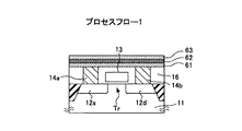
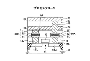
図6A〜図6Eは、図3に示すメモリセル構造を有するMRAM(半導体記憶装置)のプロセスフローの例を示す図である。 6A to 6E are diagrams showing an example of a process flow of an MRAM (semiconductor memory device) having the memory cell structure shown in FIG.
まず、図6Aに示すように、標準のCMOSロジックプロセスを用いて、半導体基板11にトランジスタTrを作成する。トランジスタのゲート電極13は、ワード線13として機能する。ワード線13の両側にソース・ドレイン不純物拡散層12s、12dが位置する。トランジスタTr上にCVD酸化膜等の層間絶縁膜16を堆積して、CMPにて表面を平坦化する。平坦化された層間絶縁膜16に、通常の配線プロセスでトランジスタTrのソース・ドレイン12s、12dに達するプラグ14a、14bを形成する。プラグ14a、14bは、コンタクトホール(不図示)内をタングステン(W)等の導体で埋め込み、CMPにて平坦化する。層間絶縁膜16およびWプラグ14a、14bの露出面上に、第1の強磁性層61、絶縁材料膜62、第2の強磁性層63を順次堆積する。この例では、図示の簡略化のため、3層の積層として図示されているが、実際は、後述するように、第1の強磁性層61の下に反強磁性層や下地層が形成され、第1の強磁性層61も単層である必要はない。
First, as shown in FIG. 6A, a transistor Tr is formed on the
次に、図6Bに示すように、層間絶縁膜16上の積層を加工して、プラグ14a、14bにそれぞれ接続するMTJ30B、30Aを形成する。図6Bでは、各MTJ30は、便宜上、第1の強磁性層61から形成されるピンド層31と、第2の強磁性層63から形成されるフリー層33と、絶縁材料膜62から形成されるトンネルバリア層32を有するように描かれている。
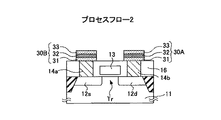
Next, as shown in FIG. 6B, the stacked layers on the
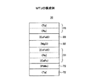
図7に、MTJ30A(又は30B)の膜構造の一例を示す。MTJ30の膜構造は、Ta下地層72と、PtMn反強磁性層73と、CoFeB/Ru/CoFeの積層構造のピンド層31と、MgOトンネルバリア層32と、CoFeBフリー層33と、Ta/Ruキャップ層75を含む。このような積層の成膜方法は、基板をスパッタ装置に入れ、真空度を1×10-7Torrにして、Arを導入して所定の圧力に設定する。基板上に、下地層72としてのTa10nm、反強磁性層73としてのPtMn15nm、CoFe(1.7nm)/Ru(0.68nm)/CoFeB(2.2nm)の3層構造のピンド層31、トンネルバリア層32としてのMgO1.2nm、フリー層33としてのCoFeB2nm、キャップ層75としてRu(10nm)/Ta(30nm)を順次堆積する。成膜温度は、室温である。フォトリソグラフィにより、最上層のTa上に、MTJのレジストパターンを形成して、反応性イオンエッチング(RIE)技術を用いて加工する。多層膜に対応して、エッチングガスを変える。第1ガスは、CF4/Arガスで、最上層のTaをエッチングする。第2ガスはCo/NH3ガスで、PtMnまでエッチングする。第3ガスはCF4/Arガスで、下地Taをエッチングする。以上により、所望の形状にパターンニングされたMTJ30を作製することができる。
FIG. 7 shows an example of the film structure of MTJ30A (or 30B). The film structure of the
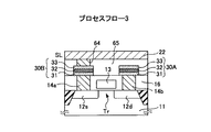
図6Cに戻って、層間絶縁膜16およびMTJ30A,30B上に層間絶縁膜65を形成して、CMPで平坦化する。次に、メモリセルのMTJの一方、たとえばMTJ30Bを、上層のソース線(SL)に接続するプラグ64を形成し、CMPで平坦化して、所定の形状のソース線22を形成する。
Returning to FIG. 6C, an
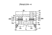
次に、図6Dに示すように、層間絶縁膜65上およびソース線22の配線パターン上に、層間絶縁膜67を堆積し、メモリセルのMTJのもう一方、たとえばMTJ30Aを、上層のビット線(BL)に接続するプラグ18を形成する。その後、CMPで平坦化する。
Next, as shown in FIG. 6D, an
次に、平坦化された層間絶縁膜67上に、所定の形状のビット線(BL)21を形成して、1T−2MTJのMRAMの基本構造が完成する。なお、図示はしないが、セルトランジスタTrのソース12sまたはドレイン12dから、読み出し用のビット線に接続されるプラグが引き出されているものとする。
Next, a bit line (BL) 21 having a predetermined shape is formed on the planarized
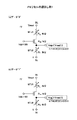
次に、図8〜図10を参照して、MRAMメモリセルの読み出し動作例を説明する。図8は、メモリセルの読み出し例1である。この例では、読み出し信号Vsigは、セルトランジスタのソース側から取り出される。スピン注入MRAMのMTJのR*A積を、20Ωμm2とし、サイズ(面積)Aを、32nm世代以降を想定して100nm×100nm=0.01μm2とすると、抵抗は2KΩとなる。これは、低抵抗状態の抵抗値(RL)になる。ここで、MTJのMR比を100%とする。高抵抗状態の抵抗値は、4KΩとなる。セルTrのON抵抗を1KΩとする。
Next, a read operation example of the MRAM memory cell will be described with reference to FIGS. FIG. 8 shows a read example 1 of the memory cell. In this example, the read signal Vsig is extracted from the source side of the cell transistor. If the MTJ R * A product of spin injection MRAM is 20 Ωμm 2 and the size (area) A is 100 nm × 100 nm = 0.01
図8(a)において、たとえば図3(c)のようにSL側からスピン電流を注入して(電子がビット線側から流れるようにして)書き込みを行なった場合、MTJ1は4KΩ、MTJ2は2KΩとなる。この状態をデータ“0”に対応する状態とする。図8(b)において、図3(d)のようにBL側からスピン電流を注入して(電子がソース線側から流れるようにして)書き込みを行なった場合、MTJ1は2KΩ、MTJ2は4KΩとなる。この状態を、データ“1”に対応する状態とする。 8A, for example, when writing is performed by injecting a spin current from the SL side (with electrons flowing from the bit line side) as shown in FIG. 3C, MTJ1 is 4 KΩ, and MTJ2 is 2 KΩ. It becomes. This state is a state corresponding to the data “0”. 8B, when writing is performed by injecting a spin current from the BL side (with electrons flowing from the source line side) as shown in FIG. 3D, MTJ1 is 2 KΩ and MTJ2 is 4 KΩ. Become. This state is a state corresponding to the data “1”.
図8(a)の状態で、BL側に1V、SL側に0Vの読出し電圧Vreadを加えると、セルトランジスタTrのソース側の電位Vsigは、
Vsig=2/7=0.29V
となる。このVsigの電圧を、読出し電圧Vreadの半分の電圧(Vread/2=0.5V)と比較すると、Vsigの方が小さく(Vsig<Vread/2)、データ“0”が書き込まれていたことが検出される。
In the state of FIG. 8A, when a read voltage Vread of 1V is applied to the BL side and 0V to the SL side, the potential Vsig on the source side of the cell transistor Tr is
Vsig = 2/7 = 0.29V
It becomes. When this Vsig voltage is compared with half of the read voltage Vread (Vread / 2 = 0.5 V), Vsig is smaller (Vsig <Vread / 2) and data “0” is written. Detected.
一方、図8(b)の状態で、BL側に1V、SL側に0Vの読出し電圧Vreadを加えると、セルトランジスタTrのソース側の電位Vsigは、
Vsig=4/7=0.57V
となる。このVsigの電圧を、読出し電圧Vreadの半分の電圧(Vread/2=0.5V)と比較すると、Vsigの方が大きく(Vsig>Vread/2)、データ“1”が書き込まれていたことが検出される。
On the other hand, when a read voltage Vread of 1V is applied to the BL side and 0V to the SL side in the state of FIG. 8B, the potential Vsig on the source side of the cell transistor Tr is
Vsig = 4/7 = 0.57V
It becomes. When this voltage Vsig is compared with half of the read voltage Vread (Vread / 2 = 0.5V), Vsig is larger (Vsig> Vread / 2) and data “1” is written. Detected.
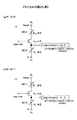
図9は、メモリセルの読み出し例2である。読み出し例1では、セルトランジスタTrのソース側から、読出し電圧Vsigを引き出したので、セルトランジスタTrのON抵抗は、MTJ1側に加わることになる。したがって、セルトランジスタTrのソース側から引き出したVsigの値は、低めに出る。読み出し例1の場合は、セルTrのON抵抗の分圧に相当する電圧であるVread×(1/7)=1V×(1/7)=0.14Vだけ、低くなる。したがって、図8(a)のデータ“0”に対応するVsig<Vread/2のときは、マージンが拡がる方向にシフトし、図8(b)のデータ“1”に対応するVsig>Vread/2のときは、マージンが狭まる方向にシフトしている。 FIG. 9 shows a read example 2 of the memory cell. In read example 1, since the read voltage Vsig is drawn from the source side of the cell transistor Tr, the ON resistance of the cell transistor Tr is added to the MTJ1 side. Therefore, the value of Vsig drawn from the source side of the cell transistor Tr appears lower. In the case of the reading example 1, the voltage is reduced by Vread × (1/7) = 1V × (1/7) = 0.14V, which is a voltage corresponding to the divided voltage of the ON resistance of the cell Tr. Therefore, when Vsig <Vread / 2 corresponding to the data “0” in FIG. 8A, the margin is shifted in the direction in which the margin increases, and Vsig> Vread / 2 corresponding to the data “1” in FIG. In this case, the margin is shifted in a narrowing direction.
このシフトをなくして、ワーストケースの読出しマージンを大きくするために、読み出し例2では、比較電圧をVread/2から、セルTrのON抵抗の分圧に相当する電圧(1/7=0.14V)の半分だけ、低い電圧に設定する。したがって、図9の読み出し例2では、読み出し電圧Vsigを0.5V−0.07=0.43Vと比較することになる。このように設定することで、図9(a)のデータ“0”の場合と、図9(b)のデータ“1”の場合で、読み出しマージンを均等にして、読み出し精度と動作の安定を実現する。 In order to eliminate this shift and increase the worst-case read margin, in read example 2, the comparison voltage is changed from Vread / 2 to a voltage corresponding to the divided voltage of the ON resistance of the cell Tr (1/7 = 0.14V). ) Is set to a low voltage by half. Therefore, in the read example 2 of FIG. 9, the read voltage Vsig is compared with 0.5V−0.07 = 0.43V. By setting in this way, the read margin and the operation stability are made uniform in the case of the data “0” in FIG. 9A and the data “1” in FIG. 9B. Realize.
図10は、メモリセルの読み出し例3である。読み出し例3では、セルトランジスタTrのドレイン側から、読出し電圧Vsigを引き出す。この場合、読み出し電圧Vsigは、セルトランジスタTrのON抵抗の分圧に相当する電圧、すなわち、Vread×(1/7)=1V×(1/7)=0.14Vだけ、高い方にシフトする。このシフトをなくして、ワーストケースの読出しマージンを大きくするために、読み出し例3では、比較電圧をVread/2から、セルTrのON抵抗の分圧に相当する電圧(1/7=0.14V)の半分だけ、高い電圧に設定する。したがって、読み出し電圧Vsigを0.5V+0.07=0.57Vと比較することになる。このように設定することで、図10(a)のデータ“0”の場合と、図10(b)のデータ“1”の場合で、読み出しマージンをほぼ均等にして、読み出し精度と動作の安定を実現する。 FIG. 10 shows a read example 3 of the memory cell. In read example 3, the read voltage Vsig is extracted from the drain side of the cell transistor Tr. In this case, the read voltage Vsig is shifted higher by a voltage corresponding to the divided voltage of the ON resistance of the cell transistor Tr, that is, Vread × (1/7) = 1V × (1/7) = 0.14V. . In order to eliminate this shift and increase the worst-case read margin, in read example 3, the comparison voltage is changed from Vread / 2 to a voltage corresponding to the divided voltage of the ON resistance of the cell Tr (1/7 = 0.14V). ) Set the voltage higher by half. Therefore, the read voltage Vsig is compared with 0.5V + 0.07 = 0.57V. By setting in this way, the read margin and the operation stability are almost equalized in the case of the data “0” in FIG. 10A and the data “1” in FIG. 10B. To realize.
上述の構成により、スピン注入MRAMにおいて、1T−1MTJメモリセルと同等な小面積で1T−2MTJメモリセルを実現し、相補的なデータの書き込み/読み出しを行うことができる。相補的な読み出しで、読み出し動作が安定する。また、電圧センス方式を採用することができるので、周辺回路が簡単になり、回路を小さく維持することが可能になる。 With the above-described configuration, in the spin injection MRAM, a 1T-2MTJ memory cell can be realized with a small area equivalent to that of the 1T-1MTJ memory cell, and complementary data writing / reading can be performed. Complementary reading stabilizes the reading operation. In addition, since the voltage sensing method can be adopted, the peripheral circuit is simplified and the circuit can be kept small.
また、実施形態の半導体記憶装置の製造方法は、
半導体基板に、トランジスタを形成し、
前記トランジスタのソースおよびドレインのそれぞれに達する第1及び第2の接続プラグを同時に形成し、
前記第1及び第2の接続プラグの各々に接続する磁気トンネル接合素子を同一プロセスで一括形成する、
工程を含む。この方法により、相補型の記憶素子を簡単な工程で作製することができる。
In addition, the method for manufacturing the semiconductor memory device of the embodiment includes:
A transistor is formed on a semiconductor substrate,
Forming first and second connection plugs reaching the source and drain of the transistor simultaneously,
A magnetic tunnel junction element connected to each of the first and second connection plugs is collectively formed in the same process;
Process. By this method, a complementary memory element can be manufactured by a simple process.
実施形態の半導体記憶装置の書き込み方法は、
トランジスタのソース電極に第1の磁気トンネル接合素子を接続し、
前記トランジスタのドレイン電極に第2の磁気トンネル接合素子を接続してメモリセルを形成し、
前記メモリセルに書き込み電流を印加して、前記第1及び第2の磁気トンネル接合素子の一方を低抵抗状態にし、他方を高抵抗状態にする、
工程を含む。
The writing method of the semiconductor memory device of the embodiment is as follows:
Connecting the first magnetic tunnel junction element to the source electrode of the transistor;
A memory cell is formed by connecting a second magnetic tunnel junction element to the drain electrode of the transistor;
A write current is applied to the memory cell to place one of the first and second magnetic tunnel junction elements in a low resistance state and the other in a high resistance state;
Process.
また、実施形態の半導体記憶装置の読み出し方法は、
トランジスタのソース電極に第1の磁気トンネル接合素子を接続し、
前記トランジスタのドレイン電極に第2の磁気トンネル接合素子を接続してメモリセルを形成し、
前記第1の磁気トンネル接合素子と、前記第2の磁気トンネル接合素子の間に読み出し電圧を印加し、前記トランジスタと、前記第1又は第2の磁気トンネル接合素子との間の接続ノードの電位を検出し、
前記検出した電位を、前記読み出し電圧の1/2の参照電位と比較して、前記メモリセルの状態を検出する、
工程を含む。
In addition, the reading method of the semiconductor memory device of the embodiment is
Connecting the first magnetic tunnel junction element to the source electrode of the transistor;
A memory cell is formed by connecting a second magnetic tunnel junction element to the drain electrode of the transistor;
A read voltage is applied between the first magnetic tunnel junction element and the second magnetic tunnel junction element, and a potential of a connection node between the transistor and the first or second magnetic tunnel junction element Detect
Comparing the detected potential with a reference potential that is ½ of the read voltage to detect the state of the memory cell;
Process.
1 スピン注入MRAM(半導体記憶装置)
11 半導体基板
12 ソース・ドレイン拡散層
13 ワード線
30、30A、30B MTJ(磁気トンネル接合素子)
31 ピンド層
32 トンネルバリア層
33 フリー層
21 ビット線(BL)
22 ソース線(SL)
Tr トランジスタ
ReadBL
読み出し専用ビット線
1 Spin injection MRAM (semiconductor memory device)
11 Semiconductor substrate 12 Source /
31 pinned
22 Source line (SL)
Tr transistor
ReadBL
Read-only bit line
Claims (6)
前記トランジスタの一方の側に接続される磁気トンネル接合素子は、ビット線方向に隣接するセルの読み出しノードに接続される第1ビット線に接続され、前記トランジスタの他方の側に配置される読み出しノードは、前記隣接するセルの磁気トンネル接合素子のひとつに接続される第2ビット線に接続されている半導体記憶装置。 Two magnetic tunnel junction elements that take complementary resistance states when a write current is applied are connected in series on both sides of the source and drain of the transistor ,
A magnetic tunnel junction element connected to one side of the transistor is connected to a first bit line connected to a read node of a cell adjacent in the bit line direction, and is a read node disposed on the other side of the transistor A semiconductor memory device connected to a second bit line connected to one of the magnetic tunnel junction elements of the adjacent cell .
前記トランジスタのソース・ドレイン拡散層の一方に電気的に接続される第1の磁気トンネル接合素子と、
前記ソース・ドレイン拡散層の他方に電気的に接続される第2の磁気トンネル接合素子と、
前記第1の磁気トンネル接合素子に接続される第1ビット線と、
前記第2の磁気トンネル接合素子と前記トランジスタの間で、前記第1及び第2の磁気トンネル接合素子の抵抗状態を検出する読み出しノードと、
前記読み出しノードに接続される第2ビット線と、
を有し、
前記第1ビット線は、当該第1ビット線方向に隣接するセルの読み出しノードに接続され、
前記第1および第2の磁気トンネル接合素子は、外部から供給される書き込み電流が、前記第1の磁気トンネル接合素子と前記第2の磁気トンネル接合素子において逆方向に流れるように、前記トランジスタに接続されることを特徴とする半導体記憶装置。 A transistor,
A first magnetic tunnel junction element electrically connected to one of the source / drain diffusion layers of the transistor;
A second magnetic tunnel junction element electrically connected to the other of the source / drain diffusion layers;
A first bit line connected to the first magnetic tunnel junction element;
A read node for detecting a resistance state of the first and second magnetic tunnel junction elements between the second magnetic tunnel junction element and the transistor;
A second bit line connected to the read node;
Have
The first bit line is connected to a read node of a cell adjacent in the first bit line direction,
The first and second magnetic tunnel junction elements are connected to the transistor so that a write current supplied from the outside flows in opposite directions in the first magnetic tunnel junction element and the second magnetic tunnel junction element. A semiconductor memory device which is connected.
をさらに有することを特徴とする請求項2又は3に記載の半導体記憶装置。 A source line connected to the second magnetic tunnel junction element ;
The semiconductor memory device according to claim 2, further comprising:
互いに隣接し、各々が1つのトランジスタと、前記トランジスタのソース・ドレインの両側に直列に接続される2つの磁気トンネル接合素子と、前記ソース・ドレインのいずれかの側に位置する読み出しノードとを有する第1及び第2のメモリセル、を含み、
前記第1のメモリセルの一方の磁気トンネル接合素子と、前記第2のメモリセルの前記読み出しノードとが接続される第1のビット線と、
前記第2のメモリセルの一方の磁気トンネル接合素子と、前記第1のメモリセルの前記読み出しノードとが接続される第2のビット線と、
を有することを特徴とする半導体記憶装置。 In a semiconductor memory device having an array of a plurality of memory cells,
Adjacent to each other, each having one transistor, two magnetic tunnel junction elements connected in series on both sides of the source / drain of the transistor, and a read node located on either side of the source / drain First and second memory cells,
A first bit line connected to one magnetic tunnel junction element of the first memory cell and the read node of the second memory cell;
A second bit line to which one magnetic tunnel junction element of the second memory cell and the read node of the first memory cell are connected;
A semiconductor memory device comprising:
Priority Applications (1)
| Application Number | Priority Date | Filing Date | Title |
|---|---|---|---|
| JP2007330271A JP5141237B2 (en) | 2007-12-21 | 2007-12-21 | Semiconductor memory device, manufacturing method thereof, writing method and reading method |
Applications Claiming Priority (1)
| Application Number | Priority Date | Filing Date | Title |
|---|---|---|---|
| JP2007330271A JP5141237B2 (en) | 2007-12-21 | 2007-12-21 | Semiconductor memory device, manufacturing method thereof, writing method and reading method |
Publications (2)
| Publication Number | Publication Date |
|---|---|
| JP2009151885A JP2009151885A (en) | 2009-07-09 |
| JP5141237B2 true JP5141237B2 (en) | 2013-02-13 |
Family
ID=40920842
Family Applications (1)
| Application Number | Title | Priority Date | Filing Date |
|---|---|---|---|
| JP2007330271A Expired - Fee Related JP5141237B2 (en) | 2007-12-21 | 2007-12-21 | Semiconductor memory device, manufacturing method thereof, writing method and reading method |
Country Status (1)
| Country | Link |
|---|---|
| JP (1) | JP5141237B2 (en) |
Families Citing this family (9)
| Publication number | Priority date | Publication date | Assignee | Title |
|---|---|---|---|---|
| JP5238430B2 (en) * | 2008-09-25 | 2013-07-17 | 株式会社東芝 | Storage device |
| JP5032611B2 (en) | 2010-02-19 | 2012-09-26 | 株式会社東芝 | Semiconductor integrated circuit |
| JP5664112B2 (en) * | 2010-10-18 | 2015-02-04 | 富士通株式会社 | Memory cell, semiconductor memory and system |
| JP2013058521A (en) * | 2011-09-07 | 2013-03-28 | Toshiba Corp | Storage device and method for manufacturing the same |
| JP5551129B2 (en) * | 2011-09-07 | 2014-07-16 | 株式会社東芝 | Storage device |
| JP5444414B2 (en) | 2012-06-04 | 2014-03-19 | 株式会社東芝 | Magnetic random access memory |
| KR102235043B1 (en) | 2014-06-09 | 2021-04-05 | 삼성전자주식회사 | Semiconductor memory device |
| CN111788672B (en) * | 2018-03-06 | 2025-02-11 | 索尼半导体解决方案公司 | Semiconductor equipment and imaging equipment |
| US11545202B2 (en) * | 2021-04-30 | 2023-01-03 | Taiwan Semiconductor Manufacturing Company, Ltd. | Circuit design and layout with high embedded memory density |
Family Cites Families (2)
| Publication number | Priority date | Publication date | Assignee | Title |
|---|---|---|---|---|
| JP3873055B2 (en) * | 2002-12-27 | 2007-01-24 | 株式会社東芝 | Semiconductor memory device |
| US7289356B2 (en) * | 2005-06-08 | 2007-10-30 | Grandis, Inc. | Fast magnetic memory devices utilizing spin transfer and magnetic elements used therein |
-
2007
- 2007-12-21 JP JP2007330271A patent/JP5141237B2/en not_active Expired - Fee Related
Also Published As
| Publication number | Publication date |
|---|---|
| JP2009151885A (en) | 2009-07-09 |
Similar Documents
| Publication | Publication Date | Title |
|---|---|---|
| JP5233234B2 (en) | Semiconductor device and manufacturing method thereof | |
| JP5141237B2 (en) | Semiconductor memory device, manufacturing method thereof, writing method and reading method | |
| JP4149647B2 (en) | Semiconductor memory device and manufacturing method thereof | |
| CN102629659B (en) | Semiconductor device | |
| US6909129B2 (en) | Magnetic random access memory | |
| US7382643B2 (en) | Magnetoresistive effect element and magnetic memory device | |
| US6657270B2 (en) | Magnetic random access memory using bipolar junction transistor, and method for fabricating the same | |
| JP2006185477A (en) | Magnetic memory device and reading method and writing method thereof | |
| US20140301135A1 (en) | Mram having novelself-referenced read method | |
| KR100542849B1 (en) | Magnetic memory device, manufacturing method thereof and data reading method thereof | |
| JP5990130B2 (en) | Semiconductor memory device | |
| US6788570B2 (en) | Magnetic random access memory | |
| KR100951068B1 (en) | Magnetic memory device and manufacturing method thereof | |
| WO2006095389A1 (en) | Magnetic memory and read/write method thereof | |
| JP2006210396A (en) | Magnetic memory device and reading method thereof | |
| JP4408901B2 (en) | Magnetic memory device and reading method thereof | |
| JP4572102B2 (en) | Heated MRAM cell to facilitate state switching | |
| JP4415745B2 (en) | Solid state memory device | |
| JP2005340300A (en) | Magnetic memory device and manufacturing method thereof | |
| JP2009218318A (en) | Semiconductor device and method of manufacturing the same | |
| US7177179B2 (en) | Magnetic memory, and its operating method | |
| JP4744532B2 (en) | Magnetic memory device and writing method thereof | |
| KR100979350B1 (en) | Magnetic ram and method of manufacturing the same | |
| US7366010B2 (en) | Magnetic memory | |
| JP3896072B2 (en) | Magnetic storage device and manufacturing method thereof |
Legal Events
| Date | Code | Title | Description |
|---|---|---|---|
| A621 | Written request for application examination |
Free format text: JAPANESE INTERMEDIATE CODE: A621 Effective date: 20100820 |
|
| A977 | Report on retrieval |
Free format text: JAPANESE INTERMEDIATE CODE: A971007 Effective date: 20120723 |
|
| A131 | Notification of reasons for refusal |
Free format text: JAPANESE INTERMEDIATE CODE: A131 Effective date: 20120731 |
|
| A521 | Request for written amendment filed |
Free format text: JAPANESE INTERMEDIATE CODE: A523 Effective date: 20120927 |
|
| TRDD | Decision of grant or rejection written | ||
| A01 | Written decision to grant a patent or to grant a registration (utility model) |
Free format text: JAPANESE INTERMEDIATE CODE: A01 Effective date: 20121023 |
|
| A01 | Written decision to grant a patent or to grant a registration (utility model) |
Free format text: JAPANESE INTERMEDIATE CODE: A01 |
|
| A61 | First payment of annual fees (during grant procedure) |
Free format text: JAPANESE INTERMEDIATE CODE: A61 Effective date: 20121105 |
|
| FPAY | Renewal fee payment (event date is renewal date of database) |
Free format text: PAYMENT UNTIL: 20151130 Year of fee payment: 3 |
|
| R150 | Certificate of patent or registration of utility model |
Free format text: JAPANESE INTERMEDIATE CODE: R150 |
|
| LAPS | Cancellation because of no payment of annual fees |